US4010323A - Digital timing recovery - Google Patents
Digital timing recovery Download PDFInfo
- Publication number
- US4010323A US4010323A US05/626,658 US62665875A US4010323A US 4010323 A US4010323 A US 4010323A US 62665875 A US62665875 A US 62665875A US 4010323 A US4010323 A US 4010323A
- Authority
- US
- United States
- Prior art keywords
- phase
- carrier wave
- samples
- timing recovery
- output
- Prior art date
- Legal status (The legal status is an assumption and is not a legal conclusion. Google has not performed a legal analysis and makes no representation as to the accuracy of the status listed.)
- Expired - Lifetime
Links
Images
Classifications
-
- H—ELECTRICITY
- H04—ELECTRIC COMMUNICATION TECHNIQUE
- H04L—TRANSMISSION OF DIGITAL INFORMATION, e.g. TELEGRAPHIC COMMUNICATION
- H04L7/00—Arrangements for synchronising receiver with transmitter
- H04L7/02—Speed or phase control by the received code signals, the signals containing no special synchronisation information
- H04L7/033—Speed or phase control by the received code signals, the signals containing no special synchronisation information using the transitions of the received signal to control the phase of the synchronising-signal-generating means, e.g. using a phase-locked loop
- H04L7/0331—Speed or phase control by the received code signals, the signals containing no special synchronisation information using the transitions of the received signal to control the phase of the synchronising-signal-generating means, e.g. using a phase-locked loop with a digital phase-locked loop [PLL] processing binary samples, e.g. add/subtract logic for correction of receiver clock
Definitions
- This invention relates generally to sample timing recovery in differentially coherent phase-shift keyed (PSK) data transmission systems and, in particular, to digital implementation of sample timing recovery in receivers for such data transmission systems.
- PSK phase-shift keyed
- the transmitter described by me employs a substantially digital implementation of a PSK modulator using a quantized "staircasing" arrangement compatible with large-scale integrated-circuit (LSI) techniques.
- the output wave produced after low-pass filtering is characterized by a substantially constant frequency with discrete phase changes occurring at synchronous modulation, i.e., baud, intervals.
- the information to be transmitted is encoded in phase changes measured between the centers of successive modulation, signaling or baud intervals. Due to this differential encoding no absolute phase reference need be transmitted with the output wave.
- Tong describes a receiver for a differentially coherent PSK signal wave using comparison detection techniques implemented by a multistage shift register and a pair of binary counters. Present and delayed replicas of received signal samples taken in successive baud intervals are correlated in exclusive-OR gates, whose outputs drive the binary counters. According to whether or not the counters have reached predetermined count thresholds the binary nature of the transmitted data bit is ascertained. The instant of time at which the observation of the attainment or not of the count threshold is important from the standpoint of the validity and freedom from error of the resultant data decision. Tong broadly indicates a baud-rate clock for sampling the counter outputs. Tong's digital demodulator is also compatible with LSI techniques.
- a sample timing recovery circuit for a differentially coherent PSK data receiver comprises an amplitude limiter for squaring up received data signals, a multistage shift register for serially storing periodic samples taken at a rate higher than the baud rate of the squared data signals, a pair of correlators for the instantly received signals and replicas thereof delayed by intervals related to the frequency of the signal carrier wave, a coincidence circuit combining the outputs of the correlators, a differentiator, a monopulser and a digital phase locked loop.
- the shift register serves as digitally implemented delay medium.
- sampling rate is selected such that each half-cycle of the carrier wave is sampled at least four times and preferably several times that number to reduce quantizing error and thus to insure adequate noise performance.
- Correlations are made between the instant input sample and samples delayed by one half-cycle (180°) of the carrier wave and also between a sample delayed from the input by a predetermined amount and a further sample delayed by an additional one half-cycle (180°) of the carrier wave.
- each of these correlations is negative.
- two positive correlations will be observed.
- Sporadic correlations due to noise can occur at any time in either correlator. It is clear that when two simultaneous positive correlations occur the phase of the carrier wave has changed by the predetermined amount. Consequently, the results of the two correlations are combined to provide a positive phase change indication.
- phase-change indication from the correlators is generated within the first quarter of most baud intervals (every baud interval except that encoding the dibit 00).
- a monopulser triggered by the first such indication in each baud interval then generates a pulse stretched over half a baud interval, i.e., has a duration equal to a half-cycle of the timing wave.
- This pulse is compared with the output of a phaselocked oscillator having a nominal frequency equal to the baud rate and by an add/delete arrangement is brought into average phase alignment with the baud intervals of the received signal wave.
- phase-locked oscillator The purpose of the phase-locked oscillator is to smooth out and largely eliminate the phase jitter superposed on the received signal.
- a uniform supplementary delay can be built into the oscillator loop to compensate for any skew or offset between the transition between baud intervals and the occurrence of the average phase change in the received wave.
- the baud rate is 600 and the carrier frequency is 1200 Hz.
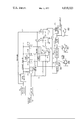
- FIGURE of the drawing showing a block diagram of a digital timing recovery arrangement for a differentially encoded PSK data transmission system, according to this invention.
- FIG. 1 In this single FIGURE of the drawing there is shown a sample timing recovery circuit comprising received PSK signal input lead 10, limiter 11, multistage shift register 13 having taps on leads 15 through 18, fixed oscillator 12, frequency divider 14, exclusive-OR gates 19 and 20, NAND-gates 21, 24 and 28, inverter 25, flip-flops 26 and 27, monopulser 30, comparator 31, fixed delay 32, phase-locked oscillator 33 and output line 35.
- Shift register 13 is substantially the same as that described in the copending Tong patent application, but with additional taps on stages 8, 64 and 72.
- 256 samples (the same number employed by Tong in his demodulator) are effectively taken in each baud interval. Since there are two cycles of the carrier wave in each baud interval, one hundred twenty-eight samples are taken in each carrier-wave cycle. Accordingly, the sample at the tap of the 64th stage is 180 electrical degrees from that at the input provided no change in phase has taken place. If, however, a change in phase does take place, the normal opposite phase condition between taps separated by 64 samples will be altered. Furthermore, the eighth tap is approximately 22.5° from the input and 72nd tap is 180° from the eighth tap. Thus, the eighth and 72nd taps provide a second set of taps at which the 180° phase difference can be monitored.
- the samples at the input on lead 15 and at the 64th tap on lead 16 are applied to exclusive-OR gate 19, whose output is high when both inputs are the same and low when they are binary opposites. Thus, as long as the inputs to exclusive-OR gates 19 are opposite, the output remains low to indicate that the samples at the input and at the 64th stage of shift register 13 are 180 degrees out of phase.
- samples at the eighth and 72nd taps are applied by way of leads 17 and 18 to exlusive-OR gate 20, whose output also remains low as long as its inputs are binary opposites.
- NAND-gate 21 The outputs of exclusive-OR gates 19 and 20 are combined in NAND-gate 21 whose output goes low when both its inputs become high and remains high otherwise.
- the low NAND-gate output indicates that the minimum preassigned 22.5° phase-shift has occurred in the received signal.
- Flip-flop 26 responds to the low input at point D to force its complementary Q output to its high state coincident with the next 614.4 kHz pulse at its C input by way of NAND gate 24.
- the high output from flip-flop 26 toggles flip-flop 27 to its high stage at output Q after a short delay determined by the short interval between pulses at the 614.4 kHz rate.
- the next high-speed clock pulse from lead 22 is applied to the C input of flip-flop 27 through inverter 25.
- NAND-gate 28 The like high outputs from flip-flops 26 and 27 are combined in NAND-gate 28 and cause the latter output to go low momentarily.
- the illustrated flip-flop arrangement functions as a digital differentiator.
- the momentary change of output state in NAND gate 28 activates monopulser (or one-shot multivibrator) 30 to generate a pulse having a duration equal to half the baud interval.
- the duration is 1/1200 second.
- Waveform 38 shown near the output of monopulser 30 is a rectangular pulse with jittery leading and trailing edges due mainly to the differences in phase-change instants between the several dibit codes.
- Monopulser 30 provides an inhibit output on lead 23 for the duration of its principal output pulse to prevent further operation of flip-flops 26 for half a baud interval. Thus, the monopulser can be triggered only once during the first half of each baud interval.
- the inhibit output is applied to NAND-gate 24 through which fast clock pulses are obtained over lead 22.
- Phase-locked oscillator 33 is a local oscillator operating nominally at the assigned baud rate, e.g., at 600 Hz in this specific example.
- the frequency of oscillator 33 can be derived by counting down from the output of fixed oscillator 12 in a well-known manner, since 614.4 kHz is the 1024 th harmonic of the baud rate.
- Oscillator 33 is connected in a loop with fixed delay unit 32 and comparator 31 by way of lead 36.
- the output of monopulser 30 is connected to another input of comparator 31. Consequently the output of comparator 31 on lead 36 is proportional to the difference in phase between the respective outputs of monopulser 30 and oscillator 33.
- Waveform 37 shown near the output of delay unit 32 in the FIGURE, suggests the appearance of its output as substantially free of jitter in contrast to the waveform 38, respresenting the output of monopulser 30.
- the phase difference monitored in comparator 31 can be employed in any conventional manner to adjust the phase of oscillator 33. If oscillator 33 has its frequency derived from fixed oscillator 12 by a countdown divider chain, the difference signal from comparator 31 can be used to add and delete pulses in the chain until substantial synchronism is attained.
- the steady output of oscillator 33 appearing on output lead 35 is represented in waveform 34 as a square wave at a frequency of 600 Hz with transitions occurring at the center of the baud interval. If a sampling window is required at the center of the baud interval rather than a sharp transition, a fixed 90-degree phase shift can be employed.
Landscapes
- Engineering & Computer Science (AREA)
- Computer Networks & Wireless Communication (AREA)
- Signal Processing (AREA)
- Digital Transmission Methods That Use Modulated Carrier Waves (AREA)
- Synchronisation In Digital Transmission Systems (AREA)
- Stabilization Of Oscillater, Synchronisation, Frequency Synthesizers (AREA)
Priority Applications (9)
| Application Number | Priority Date | Filing Date | Title |
|---|---|---|---|
| US05/626,658 US4010323A (en) | 1975-10-29 | 1975-10-29 | Digital timing recovery |
| CA260,123A CA1067152A (en) | 1975-10-29 | 1976-08-30 | Digital timing recovery |
| GB39398/76A GB1560107A (en) | 1975-10-29 | 1976-09-22 | Timing recovery circuit for a differentially coherent phase modulated data transmission system |
| FR7632074A FR2330216A1 (fr) | 1975-10-29 | 1976-10-25 | Circuit de recuperation de rythme pour un demodulateur de phase numerique |
| BE171800A BE847649A (fr) | 1975-10-29 | 1976-10-26 | Circuit de recuperation de rythme pour un demodulateur de phase numerique, |
| NLAANVRAGE7611902,A NL186361C (nl) | 1975-10-29 | 1976-10-27 | Tempeerherstelketen. |
| DE2648976A DE2648976C3 (de) | 1975-10-29 | 1976-10-28 | Zeitsteuerungsschaltung in Kombination mit einem Demodulator in einer differentiell kohärenten PSK-Datenfibertragnngsanlage |
| IT28816/76A IT1073377B (it) | 1975-10-29 | 1976-10-28 | Circuito di recupero di temporizzazione digitale |
| JP51129557A JPS5935222B2 (ja) | 1975-10-29 | 1976-10-29 | タイミング回路 |
Applications Claiming Priority (1)
| Application Number | Priority Date | Filing Date | Title |
|---|---|---|---|
| US05/626,658 US4010323A (en) | 1975-10-29 | 1975-10-29 | Digital timing recovery |
Publications (1)
| Publication Number | Publication Date |
|---|---|
| US4010323A true US4010323A (en) | 1977-03-01 |
Family
ID=24511287
Family Applications (1)
| Application Number | Title | Priority Date | Filing Date |
|---|---|---|---|
| US05/626,658 Expired - Lifetime US4010323A (en) | 1975-10-29 | 1975-10-29 | Digital timing recovery |
Country Status (9)
| Country | Link |
|---|---|
| US (1) | US4010323A (cg-RX-API-DMAC7.html) |
| JP (1) | JPS5935222B2 (cg-RX-API-DMAC7.html) |
| BE (1) | BE847649A (cg-RX-API-DMAC7.html) |
| CA (1) | CA1067152A (cg-RX-API-DMAC7.html) |
| DE (1) | DE2648976C3 (cg-RX-API-DMAC7.html) |
| FR (1) | FR2330216A1 (cg-RX-API-DMAC7.html) |
| GB (1) | GB1560107A (cg-RX-API-DMAC7.html) |
| IT (1) | IT1073377B (cg-RX-API-DMAC7.html) |
| NL (1) | NL186361C (cg-RX-API-DMAC7.html) |
Cited By (30)
| Publication number | Priority date | Publication date | Assignee | Title |
|---|---|---|---|---|
| US4114710A (en) * | 1975-08-20 | 1978-09-19 | Fujitsu Limited | Carrier regeneration circuit |
| US4151367A (en) * | 1977-04-29 | 1979-04-24 | Motorola, Inc. | Data sync acquisition in an asynchronous binary address decoder |
| US4169246A (en) * | 1976-12-06 | 1979-09-25 | Motorola, Inc. | Digital carrier correction circuit |
| US4189622A (en) * | 1975-10-17 | 1980-02-19 | Ncr Corporation | Data communication system and bit-timing circuit |
| US4215348A (en) * | 1978-04-04 | 1980-07-29 | Cselt-Centro Studi E Laboratori Telecomunicazioni S.P.A. | Method of and system for synchronizing data reception and retransmission aboard communication satellite |
| WO1981001226A1 (en) * | 1979-10-29 | 1981-04-30 | Burroughs Corp | Self synchronizing clock derivation circuit for double frequency encoded digital data |
| WO1981001225A1 (en) * | 1979-10-19 | 1981-04-30 | Burroughs Corp | Clock derivation circuit for double frequency encoded serial digital data |
| US4288874A (en) * | 1978-05-15 | 1981-09-08 | Ricoh Co., Ltd. | Timing data reproduction system |
| US4330862A (en) * | 1980-07-09 | 1982-05-18 | Bell Telephone Laboratories, Incorporated | Signal characteristic state detector using interval-count processing method |
| US4348769A (en) * | 1979-02-22 | 1982-09-07 | Te Ka De Felten & Guilleaume Fernmeldeanlagen Gmbh | Circuitry for extraction of a transmission clock signal from-modulated data transmissions |
| US4352192A (en) * | 1979-06-01 | 1982-09-28 | Thomson-Csf | Timing signal synchronization device |
| US4363002A (en) * | 1980-11-13 | 1982-12-07 | Fuller Robert M | Clock recovery apparatus for phase shift keyed encoded data |
| WO1983002207A1 (en) * | 1981-12-07 | 1983-06-23 | Motorola Inc | Digital coherent psk demodulator and detector |
| US4422176A (en) * | 1980-12-12 | 1983-12-20 | U.S. Philips Corporation | Phase sensitive detector |
| US4435687A (en) | 1979-04-16 | 1984-03-06 | North American Philips Corporation | Clock signal recovery circuit |
| US4464769A (en) * | 1980-03-11 | 1984-08-07 | Telefonaktiebolaget L M Ericsson | Method and apparatus for synchronizing a binary data signal |
| US4715047A (en) * | 1986-04-04 | 1987-12-22 | Harris Corporation | Digital differential phase shift keyed demodulator |
| US4756011A (en) * | 1986-12-24 | 1988-07-05 | Bell Communications Research, Inc. | Digital phase aligner |
| US4803680A (en) * | 1985-12-27 | 1989-02-07 | Nec Corporation | Destuffing circuit with a digital phase-locked loop |
| US4884285A (en) * | 1986-10-22 | 1989-11-28 | Jan Heynen | (DS) transmitter |
| US5022056A (en) * | 1989-10-23 | 1991-06-04 | National Semiconductor Corporation | Method and structure for digital phase synchronization |
| US5023892A (en) * | 1990-04-06 | 1991-06-11 | Printer Systems Corporation | System for detecting and correcting signal distortion |
| US5056120A (en) * | 1988-07-18 | 1991-10-08 | Fujitsu Limited | Phase adjusting circuit |
| US5131014A (en) * | 1991-04-19 | 1992-07-14 | General Instrument Corporation | Apparatus and method for recovery of multiphase modulated data |
| EP0614281A3 (en) * | 1993-02-24 | 1995-07-19 | Advanced Micro Devices Inc | Method and device for digital algorithmic high-speed data recovery. |
| US5905767A (en) * | 1995-11-07 | 1999-05-18 | Mitsubishi Denki Kabushiki Kaisha | Timing recovery apparatus and a diversity communication apparatus using the same |
| EP1148646A1 (de) * | 2000-04-19 | 2001-10-24 | TOSHIBA Electronics Europe GmbH | Verfahren zur Optimierung der Abtastung digitaler Signalwellen |
| US20040228427A1 (en) * | 2003-05-16 | 2004-11-18 | Wang Yung Da | Timing recovery loop with non-integer length |
| US20080169872A1 (en) * | 2004-01-22 | 2008-07-17 | The Regents Of The University Of Michigan | Demodulator, Chip And Method For Digital Demodulating An Fsk Signal |
| CN114244372A (zh) * | 2021-12-20 | 2022-03-25 | 杭州万高科技股份有限公司 | 一种曼彻斯特编码的定时信息恢复电路 |
Families Citing this family (2)
| Publication number | Priority date | Publication date | Assignee | Title |
|---|---|---|---|---|
| US5245484A (en) * | 1989-03-28 | 1993-09-14 | Asahi Kogaku Kogyo Kabushiki Kaisha | DPSK-demodulating apparatus |
| JP2808301B2 (ja) * | 1989-03-28 | 1998-10-08 | 旭光学工業株式会社 | データ信号再生装置 |
Citations (12)
| Publication number | Priority date | Publication date | Assignee | Title |
|---|---|---|---|---|
| US3020479A (en) * | 1960-08-15 | 1962-02-06 | Bell Telephone Labor Inc | Electric wave synchronization |
| US3209265A (en) * | 1963-07-09 | 1965-09-28 | Bell Telephone Labor Inc | Data receiver synchronizer for advancing or retarding phase of output after sampling over period of time |
| US3412206A (en) * | 1964-05-12 | 1968-11-19 | Bizet Pierre | Quaternary differential phase-shift system using only three phase-shift values and one time-shift value |
| US3479457A (en) * | 1964-05-08 | 1969-11-18 | Cit Alcatel | Method and apparatus for the demodulation of electric waves phase- or frequency-modulated by high-speed coded signals |
| US3485949A (en) * | 1966-05-02 | 1969-12-23 | Gen Dynamics Corp | Differential phase shift keying receiver with information modulated on a plurality of tones |
| US3514702A (en) * | 1967-09-26 | 1970-05-26 | Rca Corp | Digital demodulator system |
| US3619662A (en) * | 1970-11-23 | 1971-11-09 | Canadian Patents Dev | Data receiver and synchronizing system |
| US3729684A (en) * | 1971-07-01 | 1973-04-24 | Sanders Associates Inc | Data demodulator employing multiple correlations and filters |
| US3739277A (en) * | 1969-06-02 | 1973-06-12 | Hallicrafters Co | Digital data transmission system utilizing phase shift keying |
| US3758870A (en) * | 1972-02-23 | 1973-09-11 | Sanders Associates Inc | Digital demodulator |
| US3938052A (en) * | 1974-05-09 | 1976-02-10 | Teletype Corporation | Digital demodulator for phase-modulated waveforms |
| US3970945A (en) * | 1973-11-02 | 1976-07-20 | Licentia Patent-Verwaltungs-G.M.B.H. | Method and apparatus for demodulating PSK modulated oscillations |
-
1975
- 1975-10-29 US US05/626,658 patent/US4010323A/en not_active Expired - Lifetime
-
1976
- 1976-08-30 CA CA260,123A patent/CA1067152A/en not_active Expired
- 1976-09-22 GB GB39398/76A patent/GB1560107A/en not_active Expired
- 1976-10-25 FR FR7632074A patent/FR2330216A1/fr active Granted
- 1976-10-26 BE BE171800A patent/BE847649A/xx not_active IP Right Cessation
- 1976-10-27 NL NLAANVRAGE7611902,A patent/NL186361C/xx not_active IP Right Cessation
- 1976-10-28 DE DE2648976A patent/DE2648976C3/de not_active Expired
- 1976-10-28 IT IT28816/76A patent/IT1073377B/it active
- 1976-10-29 JP JP51129557A patent/JPS5935222B2/ja not_active Expired
Patent Citations (12)
| Publication number | Priority date | Publication date | Assignee | Title |
|---|---|---|---|---|
| US3020479A (en) * | 1960-08-15 | 1962-02-06 | Bell Telephone Labor Inc | Electric wave synchronization |
| US3209265A (en) * | 1963-07-09 | 1965-09-28 | Bell Telephone Labor Inc | Data receiver synchronizer for advancing or retarding phase of output after sampling over period of time |
| US3479457A (en) * | 1964-05-08 | 1969-11-18 | Cit Alcatel | Method and apparatus for the demodulation of electric waves phase- or frequency-modulated by high-speed coded signals |
| US3412206A (en) * | 1964-05-12 | 1968-11-19 | Bizet Pierre | Quaternary differential phase-shift system using only three phase-shift values and one time-shift value |
| US3485949A (en) * | 1966-05-02 | 1969-12-23 | Gen Dynamics Corp | Differential phase shift keying receiver with information modulated on a plurality of tones |
| US3514702A (en) * | 1967-09-26 | 1970-05-26 | Rca Corp | Digital demodulator system |
| US3739277A (en) * | 1969-06-02 | 1973-06-12 | Hallicrafters Co | Digital data transmission system utilizing phase shift keying |
| US3619662A (en) * | 1970-11-23 | 1971-11-09 | Canadian Patents Dev | Data receiver and synchronizing system |
| US3729684A (en) * | 1971-07-01 | 1973-04-24 | Sanders Associates Inc | Data demodulator employing multiple correlations and filters |
| US3758870A (en) * | 1972-02-23 | 1973-09-11 | Sanders Associates Inc | Digital demodulator |
| US3970945A (en) * | 1973-11-02 | 1976-07-20 | Licentia Patent-Verwaltungs-G.M.B.H. | Method and apparatus for demodulating PSK modulated oscillations |
| US3938052A (en) * | 1974-05-09 | 1976-02-10 | Teletype Corporation | Digital demodulator for phase-modulated waveforms |
Cited By (35)
| Publication number | Priority date | Publication date | Assignee | Title |
|---|---|---|---|---|
| US4114710A (en) * | 1975-08-20 | 1978-09-19 | Fujitsu Limited | Carrier regeneration circuit |
| US4189622A (en) * | 1975-10-17 | 1980-02-19 | Ncr Corporation | Data communication system and bit-timing circuit |
| US4169246A (en) * | 1976-12-06 | 1979-09-25 | Motorola, Inc. | Digital carrier correction circuit |
| US4151367A (en) * | 1977-04-29 | 1979-04-24 | Motorola, Inc. | Data sync acquisition in an asynchronous binary address decoder |
| US4215348A (en) * | 1978-04-04 | 1980-07-29 | Cselt-Centro Studi E Laboratori Telecomunicazioni S.P.A. | Method of and system for synchronizing data reception and retransmission aboard communication satellite |
| US4288874A (en) * | 1978-05-15 | 1981-09-08 | Ricoh Co., Ltd. | Timing data reproduction system |
| US4348769A (en) * | 1979-02-22 | 1982-09-07 | Te Ka De Felten & Guilleaume Fernmeldeanlagen Gmbh | Circuitry for extraction of a transmission clock signal from-modulated data transmissions |
| US4435687A (en) | 1979-04-16 | 1984-03-06 | North American Philips Corporation | Clock signal recovery circuit |
| US4352192A (en) * | 1979-06-01 | 1982-09-28 | Thomson-Csf | Timing signal synchronization device |
| US4313206A (en) * | 1979-10-19 | 1982-01-26 | Burroughs Corporation | Clock derivation circuit for double frequency encoded serial digital data |
| WO1981001225A1 (en) * | 1979-10-19 | 1981-04-30 | Burroughs Corp | Clock derivation circuit for double frequency encoded serial digital data |
| US4320525A (en) * | 1979-10-29 | 1982-03-16 | Burroughs Corporation | Self synchronizing clock derivation circuit for double frequency encoded digital data |
| WO1981001226A1 (en) * | 1979-10-29 | 1981-04-30 | Burroughs Corp | Self synchronizing clock derivation circuit for double frequency encoded digital data |
| US4464769A (en) * | 1980-03-11 | 1984-08-07 | Telefonaktiebolaget L M Ericsson | Method and apparatus for synchronizing a binary data signal |
| US4330862A (en) * | 1980-07-09 | 1982-05-18 | Bell Telephone Laboratories, Incorporated | Signal characteristic state detector using interval-count processing method |
| US4363002A (en) * | 1980-11-13 | 1982-12-07 | Fuller Robert M | Clock recovery apparatus for phase shift keyed encoded data |
| US4422176A (en) * | 1980-12-12 | 1983-12-20 | U.S. Philips Corporation | Phase sensitive detector |
| WO1983002207A1 (en) * | 1981-12-07 | 1983-06-23 | Motorola Inc | Digital coherent psk demodulator and detector |
| US4457005A (en) * | 1981-12-07 | 1984-06-26 | Motorola, Inc. | Digital coherent PSK demodulator and detector |
| US4803680A (en) * | 1985-12-27 | 1989-02-07 | Nec Corporation | Destuffing circuit with a digital phase-locked loop |
| US4715047A (en) * | 1986-04-04 | 1987-12-22 | Harris Corporation | Digital differential phase shift keyed demodulator |
| US4884285A (en) * | 1986-10-22 | 1989-11-28 | Jan Heynen | (DS) transmitter |
| US4756011A (en) * | 1986-12-24 | 1988-07-05 | Bell Communications Research, Inc. | Digital phase aligner |
| US5056120A (en) * | 1988-07-18 | 1991-10-08 | Fujitsu Limited | Phase adjusting circuit |
| US5022056A (en) * | 1989-10-23 | 1991-06-04 | National Semiconductor Corporation | Method and structure for digital phase synchronization |
| US5023892A (en) * | 1990-04-06 | 1991-06-11 | Printer Systems Corporation | System for detecting and correcting signal distortion |
| US5131014A (en) * | 1991-04-19 | 1992-07-14 | General Instrument Corporation | Apparatus and method for recovery of multiphase modulated data |
| EP0614281A3 (en) * | 1993-02-24 | 1995-07-19 | Advanced Micro Devices Inc | Method and device for digital algorithmic high-speed data recovery. |
| US5905767A (en) * | 1995-11-07 | 1999-05-18 | Mitsubishi Denki Kabushiki Kaisha | Timing recovery apparatus and a diversity communication apparatus using the same |
| EP1148646A1 (de) * | 2000-04-19 | 2001-10-24 | TOSHIBA Electronics Europe GmbH | Verfahren zur Optimierung der Abtastung digitaler Signalwellen |
| US20040228427A1 (en) * | 2003-05-16 | 2004-11-18 | Wang Yung Da | Timing recovery loop with non-integer length |
| US7149265B2 (en) | 2003-05-16 | 2006-12-12 | Visteon Global Technologies, Inc. | Timing recovery loop with non-integer length |
| US20080169872A1 (en) * | 2004-01-22 | 2008-07-17 | The Regents Of The University Of Michigan | Demodulator, Chip And Method For Digital Demodulating An Fsk Signal |
| US7881409B2 (en) | 2004-01-22 | 2011-02-01 | The Regents Of The University Of Michigan | Demodulator, chip and method for digitally demodulating an FSK signal |
| CN114244372A (zh) * | 2021-12-20 | 2022-03-25 | 杭州万高科技股份有限公司 | 一种曼彻斯特编码的定时信息恢复电路 |
Also Published As
| Publication number | Publication date |
|---|---|
| GB1560107A (en) | 1980-01-30 |
| FR2330216B1 (cg-RX-API-DMAC7.html) | 1981-10-23 |
| JPS5270705A (en) | 1977-06-13 |
| NL7611902A (nl) | 1977-05-03 |
| JPS5935222B2 (ja) | 1984-08-27 |
| NL186361B (nl) | 1990-06-01 |
| NL186361C (nl) | 1990-11-01 |
| CA1067152A (en) | 1979-11-27 |
| DE2648976B2 (de) | 1978-11-02 |
| BE847649A (fr) | 1977-02-14 |
| DE2648976C3 (de) | 1979-07-12 |
| IT1073377B (it) | 1985-04-17 |
| FR2330216A1 (fr) | 1977-05-27 |
| DE2648976A1 (de) | 1977-05-12 |
Similar Documents
| Publication | Publication Date | Title |
|---|---|---|
| US4010323A (en) | Digital timing recovery | |
| US3997847A (en) | Digital demodulator for differentially encoded phase-shift-keyed data | |
| US3571712A (en) | Digital fsk/psk detector | |
| US4057759A (en) | Communication receiving apparatus | |
| US3938052A (en) | Digital demodulator for phase-modulated waveforms | |
| US4280224A (en) | Bit synchronizer with early and late gating | |
| US3818347A (en) | Receiver for amplitude modulated quadrature carrier signals | |
| US3840821A (en) | Phase lock loop with sampling techniques for regenerating clock signal associated with data input signals | |
| US3626298A (en) | Transition tracking bit synchronization system | |
| US3729684A (en) | Data demodulator employing multiple correlations and filters | |
| US3846708A (en) | Digital demodulation of frequency-shift keyed data signals | |
| US3643023A (en) | Differential phase modulator and demodulator utilizing relative phase differences at the center of the modulation periods | |
| US4052558A (en) | Data transmission system | |
| US4288874A (en) | Timing data reproduction system | |
| IL107656A (en) | Demodulator | |
| US3654492A (en) | Code communication frame synchronization system | |
| US4330862A (en) | Signal characteristic state detector using interval-count processing method | |
| US3590386A (en) | Receiver for the reception of information pulse signals located in a prescribed transmission band | |
| US3222454A (en) | Digital comparison circuits | |
| US4233565A (en) | Method and apparatus for a PSK signal detector | |
| US5717728A (en) | Data/clock recovery circuit | |
| EP0146609A1 (en) | Manchester decoder | |
| US3601710A (en) | Digital detector for binary fsk signaling | |
| EP0162505B1 (en) | Arrangement for generating a clock signal | |
| EP0259867B1 (en) | Demodulator for psk-modulated signals |