EP0259867B1 - Demodulator for psk-modulated signals - Google Patents
Demodulator for psk-modulated signals Download PDFInfo
- Publication number
- EP0259867B1 EP0259867B1 EP87113213A EP87113213A EP0259867B1 EP 0259867 B1 EP0259867 B1 EP 0259867B1 EP 87113213 A EP87113213 A EP 87113213A EP 87113213 A EP87113213 A EP 87113213A EP 0259867 B1 EP0259867 B1 EP 0259867B1
- Authority
- EP
- European Patent Office
- Prior art keywords
- signal
- phase
- modulated
- frequency
- time
- Prior art date
- Legal status (The legal status is an assumption and is not a legal conclusion. Google has not performed a legal analysis and makes no representation as to the accuracy of the status listed.)
- Expired - Lifetime
Links
Images

Classifications
-
- H—ELECTRICITY
- H04—ELECTRIC COMMUNICATION TECHNIQUE
- H04L—TRANSMISSION OF DIGITAL INFORMATION, e.g. TELEGRAPHIC COMMUNICATION
- H04L27/00—Modulated-carrier systems
- H04L27/18—Phase-modulated carrier systems, i.e. using phase-shift keying
- H04L27/22—Demodulator circuits; Receiver circuits
Definitions
- This invention relates to PSK modulators, and more particularly to a novel demodulator for a signal which is phase-modulated so that the time average of its frequency is equal to a carrier frequency.
- the signal is converted into an intermediate frequency signal to keep the intermediate frequency stabilized and to demodulate to the original digital signal easily.
- a PSK demodulator comprising a mixer receiving a signal which is phase-modulated by a digital signal and an output signal of a variable frequency local oscillator.
- the PSK signal is inputted to a zero crossing detecting means and has the waveform shaped into a binary signal by said zero crossing detecting means, and changes from "0" to “1 and from “1 " to “0” of the binary signal are detected by a zero crossing detector, and a pulse signal shaped by a pulse shaping circuit sent to a pulse generating means in which the pulse signal is compared with a signal from a voltage controlled oscillator by a phase comparator, and the voltage controlled oscillator is controlled by a signal obtained by passing a comparison output signal through a low pass filter, and a signal having a frequency proportionate to the voltage of controlling the oscillator is sent from said oscillator to a frequency divider which divides said signal by two.
- the signal obtained thereby is inputted to an operator and exclusive logic between this signal and the input PSK signal is operated to output a signal which is delayed and also provided to an OR circuit which provides a decoded signal of the original input signal.
- the PSK modulation system in which a digital signal is transmitted with the bits "0" and “1 " in correspondence to the phases of the carrier, is extensively employed for transmission of digital signals, because of its good characteristics to noise.
- the PSK modulation system will be described in more detail.
- MSK modulation There are a lot of modulation techniques. One of them which is frequently used is an MSK modulation. In the MSK modulation, its phase of carrier is linearly increased by 180 for one time slot of the signal when the signal is "mark”, and the phase is linearly decreased by 180 ° for one time slot of the signal when the signal is "space”.
- the MSK system is advantageous in that, as the phase is changed linearly, the occupied frequency bandwidth is narrow.
- the DSK system is advantageous in that it, having good characteristics under condition of multi-path fading, is suitable for wide-band and high speed data transmission.
- signals received are divided into two ways. One is supplied to a phase comparator after being delayed by appropriate time duration with a delay circuit, while the other is supplied to the phase comparator as it is, so as to demodulate the PSK-modulated signal thereby to obtain the origianl digital signal.
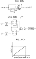
- a delay detector shown in Fig. 3(A) its input voltage Vin is represented by the following expression: where f2 is the angular frequency of a carrier, t is the time, and e(t) is the phase modulation function.
- the input voltage Vin is divided into two ways. One of the two ways is applied to one input terminal of a phase comparator 22, while the other is applied to the other input terminal of the comparator 22 after being delayed by a predetermined period of time TR. Therefore, the signal Vc applied to the one input terminal is: and the signal Vd applied to the other input terminal is: where the phase comparator 22 is designed as shown in Fig. 3 (B) and provides an output proportional to a phase difference as shown in Fig. 3(C). Therefore, the phase difference A 0 is:
- the reference point for phase comparison can be set at the center of the range of operation of the phase comparator.
- the output of the phase comparator will be the one corresponding to the operation point which is shifted as much as ⁇ (t) - 0 (t - TR) from the reference point.
- phase function ⁇ (t) is as shown in Fig. 4 (A) and ⁇ (t - T/2) is as shown in Fig. 4(B).
- ⁇ (t) - ⁇ (t - T/2) is ⁇ /2 for a "mark” period and - ⁇ /2 for a "space” period
- an output waveform as shown in Fig. 4(E) is obtained according to an output characteristic as shown in Fig. 4(D). That is, the output is 3Vo/4 for the "mark” period, and Vo/4 for the "space” period.
- a signal received is divided into two parts, which are applied to two phase comparators, respectively.
- An output signal of a voltage-controlled oscillator in a phase locked loop(whose frequency is coincident with the carrier frequency of the signal received) is applied to one of the phase comparators, and the output signal is supplied to the other phase comparator with its phase shifted by 90 °, so that the original digital signal is obtained from the output signals of the two phase comparators (cf.Trans.IECE Japan, Vol. 64-B, No.10, 1981, GMSK Modulation System Transmission Characteristic by Kazuaki Murota and Kenkichi Hiraide).
- the signal received is divided into two parts, one of which is merely delayed. This has the advantage that the circuitry can be simplified. However, if this method is applied to the transmission of digital signals in a high frequency band, the demodulation reliability is lowered.
- the operating reference point being affected by noise, and interference waves coming through multiple paths in addition to the temperature variation, is further shifted. Therefore, it is difficult to determine the "mark" and "space” through comparison of the output level of the phase comparator with a predetermined reference value.
- the synchronous detection system descibed above is based on the reproduction of a carrier frequency by a COSTAS loop.
- the difficulty due to the frequency variation never takes place, and the signal can be demodulated with high accuracy.
- the synchronous detection system has its own disadvantages. It is necessary to provide a voltage-controlled oscillator as a local oscillator and a phase locked loop to obtain the signal whose frequency is equal to the carrier frequency of a signal received. This requirement will make the circuitry intricate and increase the manufacturing cost. This problem is a serious matter especially for mobile radio equipment because of the requirement for a miniaturization and simplification of the mobile radio equipment and for a reduced manufacturing cost.
- the inventor has also proposed (in EP-A-0 257 301 filed July 21, 1987, the disclosure of which is incorporated herein by reference) two other PSK modem systems in which demodulation is based on the time average of the instantaneous angular frequencies of two respective kinds of PSK modulation waves.
- the PSK modulation wave has reference phase parts whose total time is a predetermined value provided at the front and/or rear part of one time slot of a digital pulse signal, and in the front half of the remaining part of the time slot, the phase is changed in a predetermined direction in correspondence to one of the "mark" and "space” states of a transmission signal, and in the rear half, the phase is restored to the reference phase.
- phase For the other state of the transmission signal the phase changes in the opposite direction from that of the one state.
- a PSK modulation wave is used in which the phase of the transmission signal for one of the "mark" and "space” states is as described above for the first system; however, only the reference phase part is formed over the entire range of one time slot of the digital pulse signal in correspondence to the other state of the transmission signal.
- the time average of the instantaneous angular frequencies is equal to the carrier angular frequency.
- a local oscillation frequency to be mixed with the received signal is feedback- controlled by the utilization of a signal which is obtained by subjecting an intermediate frequency signal to frequency detection, thereby to stabilize the carrier wave angular frequency of the intermediate frequency signal, and the signal received is demodulated by the utilization of the signal thus stabilized.
- a detector having a linear frequency response is, in general, employed as a frequency detector for subjecting the intermediate frequency signal to frequency detection.
- the linear detector being made up of analog circuits, has a relatively large fluctuation characteristic. Accordingly, it is essential to adjust each of the demodulators to allow the latter to operate as required. Especially in a mass production of the demodulators, the time and labor required for such adjustment will increase the manufacturing cost.
- an object of this invention is to provide a demodulator for demodulating with high accuracy a signal which is PSK-modulated according to either of the above-described other PSK modem systems.
- Another object of the invention is to provide a demodulator for demodulating a signal which is PSK-modulated according to the above-described other PSK modem systems which has a simplified construction and which has no need for adjustment during manufacture.
- a demodulator which comprises: a mixer receiving: (1) a signal which is phase-modulated such that a time average value of frequencies thereof are equal to a carrier frequency thereof, and (2) an output signal of a variable frequency local oscillator; a waveform conversion circuit for subjecting an intermediate frequency signal of the mixer to waveform conversion to obtain a square wave signal; a pulse counter for counting the square wave signal every period which is n times a time slot of a digital pulse signal (where n is an integer or a sufficiently large number other than an integer); a subtraction circuit for receiving a count number from the pulse counter to provide a difference signal between the count number and a reference count number n foT (where f o is the reference intermediate frequency band carrier frequency, and T is the time slot of the signal); a digital to analog (D/A) converter for converting the difference signal from the subtraction circuit into an analog signal which is supplied to the variable frequency local oscillator; and a restoring circuit which receives the square wave
- the above-described modulated signal which is so phase-modulated that the time average value of frequencies are equal to the carrier frequency may be of the type which is phase-modulated in such a manner that reference phase parts of predetermined total time are provided at the front and/or rear part of a time slot of a digital pulse signal, and in the front half of the remaining part of the time slot, the phase thereof is changed in a predetermined direction in correspondence to one of "mark" and "space” states of a transmission signal, while in the rear half of the remaining part, the phase thus changed is returned to a reference value, and wherein the phase is further changed in a direction opposite to the predetermined direction for the other state.
- the modulated signal may be so phase-modulated that reference phase parts of predetermined total time are provided at the front and/or rear part of a time slot of a digital pulse signal, and in the front half of the remaining part of the time slot, the phase thereof is changed in a predetermined direction in correspondence to one of "mark" and "space” states of a transmission signal, while in the rear half of the remaining part, the phase thus changed is returned to a reference value, and wherein the phase is maintained at the reference value for the other state.
- the restoring circuit may be, for example, a phase detection circuit, although this is not limitative of the invention.
- the intermediate frequency is converted into a square wave signal, the pulses are counted for a predetermined period of time, and the resultant count value is divided by the counting time. Therefore, the carrier frequency of the intermediate frequency signal can be stabilized by controlling the variable frequency local oscillator according to the difference signal which is produced by the difference between the count number and the reference count number, instead of using an analog type frequency detector. Accordingly, the carrier frequency of the intermediate frequency signal can be stabilized merely by setting the reference count value. Thus, an adjustment operation which is required in the case of an analog type frequency detector can be eliminated according to the invention.
- Fig. 2 shows examples of a modulation signal which is to be demodulated.
- reference phase parts having periods of time t1 and t2 are provided respectively before and after a phase change part of a transmission signal.
- AT is a predetermined period of time shorter than one time slot T of a digital signal.
- the phase change in the remaining part of the time slot is the same as that in the case of Figs. 2(A) and (B).
- Fig. 2 (D) shows a "space" signal in which the phase ⁇ (t) is ⁇ 0 with 0 ⁇ t ⁇ ⁇ T, ⁇ 0 - g(t- ⁇ T) with ⁇ T ⁇ t ⁇ ⁇ T + T'/2 and ⁇ 0 - g(T - t) with AT + T'/2 ⁇ t ⁇ T.
- g(t) is the phase change function
- T'/2 is the time which is a half (1/2) of the time of the part other than the reference phase part.
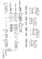
- Fig. 1 is a block diagram showing essential parts of one example of a demodulator according to this invention.
- a signal received (having an angular frequency of ⁇ ) is supplied to a mixer 2 which receives a local oscillation signal (having an angular frequency of ⁇ ) from a local oscillator, namely, a voltage-controlled oscillator (hereinafter referred to as "a VCO") 1.
- the output signal of the mixer 2 is supplied through a band-pass filter 3 and an amplifier 4 to a Schmitt trigger circuit 5, the output of which is applied to a phase detection circuit 6.
- a part of the output signal from the Schmitt trigger circuit 5 is applied through a gate circuit 7 to a pulse counter 8, the output of which is supplied through a pulse count number reading circuit 9 and a pulse count number memory 10 to a subtraction circuit 11.
- the output difference signal of the subtraction circuit is applied through a D/A (digital-to-analog) converter 12 and a low-pass filter 13 to the VCO 1.
- a reference pulse signal provided by a reference pulse number memory 14 is also supplied to the subtraction circuit 11.
- a gate control signal corresponding to a period which is an integer n times a time slot of a digital pulse signal is applied to the gate circuit 7.
- a reset signal is supplied to the pulse counter every period which is an integer n times the time slot of the digital pulse signal.
- a read control signal is applied to the pulse count number reading circuit 9 in correspondence to the reset signal supplied to pulse counter 8.
- the demodulator thus constructed operates as follows.
- a PSK modulation wave having the phase variation characteristic as shown in Fig. 2 is represented by the following expression:
- the instantaneous angular frequency of the PSK modulation wave is:
- the average value of the instantaneous angular frequencies in a time slot is:
- the average value of the instantaneous angular frequencies in a time slot is also Q.
- the time average value of the instantaneous angular frequencies of the PSK modulation wave is always equal to the angular frequency f2 of the carrier wave irrespective of the contents of the signal. This is unique because in the conventional PSK modulation wave the time average value of the instantaneous angular frequencies is not always equal to the angular frequency of the carrier wave.
- a PSK modulating signal having a carrier angular frequency of f2 S is mixed with a signal having a carrier angular frequency of ⁇ L provided by the VCO 1, to obtain a signal having an intermediate carrier angular frequency Q.
- the signal thus obtained is applied to the band-pass filter 3, where noise components, etc. are removed therefrom.
- the output of the filter 3 is amplified by the amplifier 4 to a predetermined level.
- the output signal of the amplifier 4 is converted into a square wave signal by the Schmitt trigger circuit 5, which is supplied to the phase detection circuit 6 to obtain the original digital data.
- the phase detection circuit may be the delay detection circuit illustrated in Figs. 3A, 3B and 3C.
- a part of the output signal of the Schmitt trigger circuit is supplied through the gate circuit 7 to the pulse counter 8, so that pulses are counted for a predetermined period of time.
- the resultant count value is read by the pulse count number reading circuit 9 and is stored in the pulse count number memory 10.
- the difference between the count number stored in the memory 10 and the reference pulse number memory 14 is calculated by the subtraction circuit 11.
- the difference is converted into analog data by the D/A converter 12, which is supplied to the low-pass filter 13 so that the digital error is smoothed.
- the output of the filter 13 is supplied to the VCO 1, as a result of which the oscillation frequency of the VCO is so controlled that the difference between the two count numbers is zero (0).
- the intermediate carrier angular frequency provided by the mixer 2 can be stabilized to a predetermined angular frequency.
- the above-described control may be modified as follows: After the count value of the pulse counter 8 is read, the content of the latter 8 is reset, and the gate circuit is opened. This operation is repeatedly carried out, so that the content of the pulse count number memory 10 is renewed at each operation, whereby the intermediate carrier angular frequency is continuously stabilized.
- the PSK modulation wave with the intermediate carrier angular frequency thus stabilized is applied to the phase detection circuit 6. Therefore, the phase detection can be stability achieved without decreasing the value ⁇ T.
- the phase detection is carried out with the intermediate carrier angular frequency stabilized. Therefore, the data AT can be set to a relatively large value, and the occupied frequency bandwidth of the modulation wave can be decreased.
- the demodulation of the invention after the signal is received which has been so phase-modulated that the time average value of the frequencies is equal to the carrier frequency, the received signal is mixed with the output signal of the variable frequency local oscillator in a digital-feedback-loop to obtain the intermediate frequency signal with the intermediate carrier frequency stabilized. Therefore, the original digital signal can be obtained readily and accurately without being affected by carrier frequency variations. In addition, the occurrence of product errors can be prevented.
- the invention can demodulate a signal which has been phase-modulated in such a manner that, for instance, the phase change part is formed when the transmission signal is in one of the "mark" and "space” states, and only the reference phase part is formed when it is in the other state.
Description
- This invention relates to PSK modulators, and more particularly to a novel demodulator for a signal which is phase-modulated so that the time average of its frequency is equal to a carrier frequency. The signal is converted into an intermediate frequency signal to keep the intermediate frequency stabilized and to demodulate to the original digital signal easily.
- from patent abstracts of Japan, Vol. 10, No. 75 (E-390) [21,32], March 25, 1986, and JP-A-60220650 a PSK demodulator is known comprising a mixer receiving a signal which is phase-modulated by a digital signal and an output signal of a variable frequency local oscillator. The PSK signal is inputted to a zero crossing detecting means and has the waveform shaped into a binary signal by said zero crossing detecting means, and changes from "0" to "1 and from "1 " to "0" of the binary signal are detected by a zero crossing detector, and a pulse signal shaped by a pulse shaping circuit sent to a pulse generating means in which the pulse signal is compared with a signal from a voltage controlled oscillator by a phase comparator, and the voltage controlled oscillator is controlled by a signal obtained by passing a comparison output signal through a low pass filter, and a signal having a frequency proportionate to the voltage of controlling the oscillator is sent from said oscillator to a frequency divider which divides said signal by two. The signal obtained thereby is inputted to an operator and exclusive logic between this signal and the input PSK signal is operated to output a signal which is delayed and also provided to an OR circuit which provides a decoded signal of the original input signal.
- So far, the PSK modulation system, in which a digital signal is transmitted with the bits "0" and "1 " in correspondence to the phases of the carrier, is extensively employed for transmission of digital signals, because of its good characteristics to noise.
- The PSK modulation system will be described in more detail.
- There are a lot of modulation techniques. One of them which is frequently used is an MSK modulation. In the MSK modulation, its phase of carrier is linearly increased by 180 for one time slot of the signal when the signal is "mark", and the phase is linearly decreased by 180 ° for one time slot of the signal when the signal is "space".
- Another modulation technique in a so-called "DSK" system is known, in which, as shown in Fig. 6, one time slot is divided into two equal parts and its phase of carrier is increased by two steps, namely 90 each, for the one time slot for "mark" signal, the phase is decreased also by two steps, 90 each for "space" signal.
- The MSK system is advantageous in that, as the phase is changed linearly, the occupied frequency bandwidth is narrow. The DSK system is advantageous in that it, having good characteristics under condition of multi-path fading, is suitable for wide-band and high speed data transmission.
- There are two commonly used demodulation techniques for PSK-modulated signals: synchronous detection and delay detection.
- In the delay detection, signals received are divided into two ways. One is supplied to a phase comparator after being delayed by appropriate time duration with a delay circuit, while the other is supplied to the phase comparator as it is, so as to demodulate the PSK-modulated signal thereby to obtain the origianl digital signal.
- This will be described in more detail. It is assumed that, in a delay detector shown in Fig. 3(A), its input voltage Vin is represented by the following expression:

phase comparator 22, while the other is applied to the other input terminal of thecomparator 22 after being delayed by a predetermined period of time TR. Therefore, the signal Vc applied to the one input terminal is:

phase comparator 22 is designed as shown in Fig. 3 (B) and provides an output proportional to a phase difference as shown in Fig. 3(C). Therefore, thephase difference A 0 is:
- The delay time TR should meet TR = T/2 (where T is one time slot of the signal) in the MSK system or DSK system.
- With Q TR = (2n - 1), namely with Q = (2n-1)n/TR = (2n - 1)2n / T, the reference point for phase comparison can be set at the center of the range of operation of the phase comparator.
- The operation of the DSK modulation will be described by way of example; however, it sould be noted that the description is applicable to the MSK system as well.
- In the case of e(t) - e(t - TR) = 0,
- the operation reference point of the phase comparator is expressed as

- In the case where the signal is of "mark" followed by "space", the phase function θ(t) is as shown in Fig. 4 (A) and θ(t - T/2) is as shown in Fig. 4(B).
- Accordingly, θ(t) - θ(t - T/2), as shown in Fig. 4(C) is π/2 for a "mark" period and - π/2 for a "space" period, and an output waveform as shown in Fig. 4(E) is obtained according to an output characteristic as shown in Fig. 4(D). That is, the output is 3Vo/4 for the "mark" period, and Vo/4 for the "space" period.
- Accordingly, when the output of the
phase comparator 22 exceeds Vo/2, the signal is judged as "mark". When the output is lower than Vo/2, the signal is in "space" state. - On the other hand, when a synchronous detection circuit is used for demodulation, a signal received is divided into two parts, which are applied to two phase comparators, respectively. An output signal of a voltage-controlled oscillator in a phase locked loop(whose frequency is coincident with the carrier frequency of the signal received) is applied to one of the phase comparators, and the output signal is supplied to the other phase comparator with its phase shifted by 90 °, so that the original digital signal is obtained from the output signals of the two phase comparators (cf.Trans.IECE Japan, Vol. 64-B, No.10, 1981, GMSK Modulation System Transmission Characteristic by Kazuaki Murota and Kenkichi Hiraide).
- In demodulating the PSK-modulated signal according to the above-described delay detection system, the signal received is divided into two parts, one of which is merely delayed. This has the advantage that the circuitry can be simplified. However, if this method is applied to the transmission of digital signals in a high frequency band, the demodulation reliability is lowered.
- This will be described in more detail. In the delay detection system, the operating reference point is Δθ = Q T/2. Therefore, if the carrier angular frequency drifts by A Q, for instance, by a temperature change, then the operating reference point will be changed by A Q T/2. If this change is large, then it is difficult to determine the "mark" and "space" according to whether or not the output level of the phase comparator exceeds Vo/2. For instance when the carrier frequency is 2.5 GHz, and the temperature variation of the oscillator (such as a saw tooth wave oscillator) is ± 3 x 10⁻⁴, then the frequency variation will be of ± 750 KHz. If, in this case, the data transmission speed is set to 32K bps, then T = 1/32 msec, and ΔΩ T/2 = 23.44π; that is, the drift of the operating reference point is aobut substantially 23,44π. In practice, the operating reference point, being affected by noise, and interference waves coming through multiple paths in addition to the temperature variation, is further shifted. Therefore, it is difficult to determine the "mark" and "space" through comparison of the output level of the phase comparator with a predetermined reference value.
- The synchronous detection system descibed above is based on the reproduction of a carrier frequency by a COSTAS loop. In this system, unlike the phase delay detection system, the difficulty due to the frequency variation never takes place, and the signal can be demodulated with high accuracy.
- However, the synchronous detection system has its own disadvantages. It is necessary to provide a voltage-controlled oscillator as a local oscillator and a phase locked loop to obtain the signal whose frequency is equal to the carrier frequency of a signal received. This requirement will make the circuitry intricate and increase the manufacturing cost. This problem is a serious matter especially for mobile radio equipment because of the requirement for a miniaturization and simplification of the mobile radio equipment and for a reduced manufacturing cost.
- The present inventor has proposed (in EP-A-0 254 175 filed July 13, 1987, the disclosure of which is incorporated herein by reference) a system in which the delay time is made equal to the total time of the reference phase parts of a PSK-modulation signal according to an NRZ signal obtained after demodulation of the modulated signal in order to reduce the total time of the reference phase parts, and the variation ΔeΔT of the operating reference point is thereby decreased to improve stability.
- While this proposal is advantageous, if it is employed in a system where high frequencies are used for carrier frequencies, the improvement in stability is limited, and the degree of technical difficulty is increased.
- This will be descrived in more detail. If the total time of the reference phase parts is decreased, then the rate of variation of phase to time is increased, and the occupied frequency band width of the modulation wave is increased. Furthermore, steep pulse waves must be handled in the signal (e.g. video) processing stage after detection; that is, high frequency components must be processed. This increases the degree of technical difficulty and increases costs.
- The inventor has also proposed (in EP-A-0 257 301 filed July 21, 1987, the disclosure of which is incorporated herein by reference) two other PSK modem systems in which demodulation is based on the time average of the instantaneous angular frequencies of two respective kinds of PSK modulation waves. In one of the other systems, the PSK modulation wave has reference phase parts whose total time is a predetermined value provided at the front and/or rear part of one time slot of a digital pulse signal, and in the front half of the remaining part of the time slot, the phase is changed in a predetermined direction in correspondence to one of the "mark" and "space" states of a transmission signal, and in the rear half, the phase is restored to the reference phase. For the other state of the transmission signal the phase changes in the opposite direction from that of the one state. In the second one of the other systems a PSK modulation wave is used in which the phase of the transmission signal for one of the "mark" and "space" states is as described above for the first system; however, only the reference phase part is formed over the entire range of one time slot of the digital pulse signal in correspondence to the other state of the transmission signal. In such systems the time average of the instantaneous angular frequencies is equal to the carrier angular frequency. A local oscillation frequency to be mixed with the received signal is feedback- controlled by the utilization of a signal which is obtained by subjecting an intermediate frequency signal to frequency detection, thereby to stabilize the carrier wave angular frequency of the intermediate frequency signal, and the signal received is demodulated by the utilization of the signal thus stabilized.
- In such systems, a detector having a linear frequency response is, in general, employed as a frequency detector for subjecting the intermediate frequency signal to frequency detection. The linear detector, being made up of analog circuits, has a relatively large fluctuation characteristic. Accordingly, it is essential to adjust each of the demodulators to allow the latter to operate as required. Especially in a mass production of the demodulators, the time and labor required for such adjustment will increase the manufacturing cost.
- In view of the foregoing, an object of this invention is to provide a demodulator for demodulating with high accuracy a signal which is PSK-modulated according to either of the above-described other PSK modem systems.
- Another object of the invention is to provide a demodulator for demodulating a signal which is PSK-modulated according to the above-described other PSK modem systems which has a simplified construction and which has no need for adjustment during manufacture.
- The foregoing objects of the invention have been achieved by the provision of a demodulator which comprises: a mixer receiving: (1) a signal which is phase-modulated such that a time average value of frequencies thereof are equal to a carrier frequency thereof, and (2) an output signal of a variable frequency local oscillator; a waveform conversion circuit for subjecting an intermediate frequency signal of the mixer to waveform conversion to obtain a square wave signal; a pulse counter for counting the square wave signal every period which is n times a time slot of a digital pulse signal (where n is an integer or a sufficiently large number other than an integer); a subtraction circuit for receiving a count number from the pulse counter to provide a difference signal between the count number and a reference count number n foT (where fo is the reference intermediate frequency band carrier frequency, and T is the time slot of the signal); a digital to analog (D/A) converter for converting the difference signal from the subtraction circuit into an analog signal which is supplied to the variable frequency local oscillator; and a restoring circuit which receives the square wave signal and restores it to a predetermined digital signal.
- The above-described modulated signal which is so phase-modulated that the time average value of frequencies are equal to the carrier frequency may be of the type which is phase-modulated in such a manner that reference phase parts of predetermined total time are provided at the front and/or rear part of a time slot of a digital pulse signal, and in the front half of the remaining part of the time slot, the phase thereof is changed in a predetermined direction in correspondence to one of "mark" and "space" states of a transmission signal, while in the rear half of the remaining part, the phase thus changed is returned to a reference value, and wherein the phase is further changed in a direction opposite to the predetermined direction for the other state. Alternatively, the modulated signal may be so phase-modulated that reference phase parts of predetermined total time are provided at the front and/or rear part of a time slot of a digital pulse signal, and in the front half of the remaining part of the time slot, the phase thereof is changed in a predetermined direction in correspondence to one of "mark" and "space" states of a transmission signal, while in the rear half of the remaining part, the phase thus changed is returned to a reference value, and wherein the phase is maintained at the reference value for the other state.
- The restoring circuit may be, for example, a phase detection circuit, although this is not limitative of the invention.
- The intermediate frequency is converted into a square wave signal, the pulses are counted for a predetermined period of time, and the resultant count value is divided by the counting time. Therefore, the carrier frequency of the intermediate frequency signal can be stabilized by controlling the variable frequency local oscillator according to the difference signal which is produced by the difference between the count number and the reference count number, instead of using an analog type frequency detector. Accordingly, the carrier frequency of the intermediate frequency signal can be stabilized merely by setting the reference count value. Thus, an adjustment operation which is required in the case of an analog type frequency detector can be eliminated according to the invention.
- The above and other objects, advantages and features of the invention will be more readily understood from the following detailed description of the invention which is provided in connection with the accompanying drawings wherein:
- Fig. 1 is a circuit diagram showing essential parts of one example of a demodulator according to this invention.
- Fig. 2 is a diagram for a description of one example of a modulation signal which may be demodulated by the demodulator.
- Fig. 3 is a diagram for a description of a conventional delay detector.
- Fig. 4 is a diagram for a description of the operation of the conventional delay detector shown in Fig. 3.
- Fig. 5 and 6 are diagrams for a description of conventional PSK modulation systems.
- One embodiment of the demodulation of this invention will now be described with reference to the accompanying drawings.
- Fig. 2 shows examples of a modulation signal which is to be demodulated. In Figs. 2(A) and (B), reference phase parts having periods of time t1 and t2 are provided respectively before and after a phase change part of a transmission signal. The

- Fig. 2(C) and (D) show the case where t1 = ΔT, and t2 = 0. The phase change in the remaining part of the time slot is the same as that in the case of Figs. 2(A) and (B).
- It should be noted that the phase characteristics of Figs. 2(A) and (B) are equal to those of Figs. 2(C) and (D). That is, the phase characteristic is maintained unchanged as long as ti + t2 = AT is satisfied, as will become more apparent later. Therefore, only the signal of Figs. 2(C) and (D) will be described, with delay time R set to ΔT.
- Fig. 2 (C) shows a "mark" signal in which the phase θ(t) is θ0 with 0 ≦ t < ΔT(θ0 = 0 in the figure), θ0 + g(t - ΔT) with ΔT ≦ t < AT + T'/2, and θ0 + g(T - t) with AT + T'/2 ≦ t < T.
- Fig. 2 (D) shows a "space" signal in which the phase θ(t) is θ0 with 0 ≦t < ΔT, θ0 - g(t-ΔT) with ΔT≦ t < ΔT + T'/2 and θ0 - g(T - t) with AT + T'/2 ≦t < T.
- In these expressions, g(t) is the phase change function, and T'/2 is the time which is a half (1/2) of the time of the part other than the reference phase part.
- Fig. 1 is a block diagram showing essential parts of one example of a demodulator according to this invention. In Fig. 1, a signal received (having an angular frequency of Ω) is supplied to a
mixer 2 which receives a local oscillation signal (having an angular frequency of Ω) from a local oscillator, namely, a voltage-controlled oscillator (hereinafter referred to as "a VCO") 1. The output signal of themixer 2 is supplied through a band-pass filter 3 and anamplifier 4 to aSchmitt trigger circuit 5, the output of which is applied to aphase detection circuit 6. A part of the output signal from theSchmitt trigger circuit 5 is applied through agate circuit 7 to apulse counter 8, the output of which is supplied through a pulse countnumber reading circuit 9 and a pulsecount number memory 10 to asubtraction circuit 11. The output difference signal of the subtraction circuit is applied through a D/A (digital-to-analog)converter 12 and a low-pass filter 13 to theVCO 1. A reference pulse signal provided by a referencepulse number memory 14 is also supplied to thesubtraction circuit 11. A gate control signal corresponding to a period which is an integer n times a time slot of a digital pulse signal is applied to thegate circuit 7. A reset signal is supplied to the pulse counter every period which is an integer n times the time slot of the digital pulse signal. A read control signal is applied to the pulse countnumber reading circuit 9 in correspondence to the reset signal supplied topulse counter 8. - The demodulator thus constructed operates as follows.
- In general, a PSK modulation wave having the phase variation characteristic as shown in Fig. 2 is represented by the following expression:


- Therefore, in the case of a "mark" signal, the instantaneous angular frequency is:
- ω(t) = Ω for a period of time defined by 0 ≦ t < ΔT;
- ω(t) = Ω + g'(t - ΔT) for a period of time defined by AT <t < AT + T'/2; and
- ω(t) = Ω - g'(T - t) for a period of time defined by ΔT+ T'/2 ≦ t < T.
- In the case of a "space" signal, the instantaneous angular frequency is:
- ω(t) = Q for a period of time defined by 0 ≦ t < ΔT;
- ω(t) = Ω - g'(t - ΔT) for a period of time defined by AT + T'/2 <t < T.
- In the case of the "mark" signal, the average value of the instantaneous angular frequencies in a time slot is:


- In the case of the "space" signal, the average value of the instantaneous angular frequencies in a time slot is also Q.
- The time average value of the instantaneous angular frequencies of the PSK modulation wave is always equal to the angular frequency f2 of the carrier wave irrespective of the contents of the signal. This is unique because in the conventional PSK modulation wave the time average value of the instantaneous angular frequencies is not always equal to the angular frequency of the carrier wave.
- Now, the operation of the demodulator under the above-described conditions will be described.
- A PSK modulating signal having a carrier angular frequency of f2 S is mixed with a signal having a carrier angular frequency of Ω L provided by the
VCO 1, to obtain a signal having an intermediate carrier angular frequency Q. The signal thus obtained is applied to the band-pass filter 3, where noise components, etc. are removed therefrom. The output of thefilter 3 is amplified by theamplifier 4 to a predetermined level. The output signal of theamplifier 4 is converted into a square wave signal by theSchmitt trigger circuit 5, which is supplied to thephase detection circuit 6 to obtain the original digital data. The phase detection circuit may be the delay detection circuit illustrated in Figs. 3A, 3B and 3C. - A part of the output signal of the Schmitt trigger circuit is supplied through the
gate circuit 7 to thepulse counter 8, so that pulses are counted for a predetermined period of time. The resultant count value is read by the pulse countnumber reading circuit 9 and is stored in the pulsecount number memory 10. The difference between the count number stored in thememory 10 and the referencepulse number memory 14 is calculated by thesubtraction circuit 11. The difference is converted into analog data by the D/A converter 12, which is supplied to the low-pass filter 13 so that the digital error is smoothed. The output of thefilter 13 is supplied to theVCO 1, as a result of which the oscillation frequency of the VCO is so controlled that the difference between the two count numbers is zero (0). - Thus, the intermediate carrier angular frequency provided by the
mixer 2 can be stabilized to a predetermined angular frequency. - The above-described control may be modified as follows: After the count value of the
pulse counter 8 is read, the content of the latter 8 is reset, and the gate circuit is opened. This operation is repeatedly carried out, so that the content of the pulsecount number memory 10 is renewed at each operation, whereby the intermediate carrier angular frequency is continuously stabilized. - The PSK modulation wave with the intermediate carrier angular frequency thus stabilized is applied to the
phase detection circuit 6. Therefore, the phase detection can be stability achieved without decreasing the value ΔT. - In the above-described embodiment, the phase detection is carried out with the intermediate carrier angular frequency stabilized. Therefore, the data AT can be set to a relatively large value, and the occupied frequency bandwidth of the modulation wave can be decreased. In addition, it is possible to eliminate high frequency components also a subsequent signal, e.g., video, processing stage after the detection. This will permit an increase in the degree of design freedom and improve economic operation.
- Since, as is apparent from the above description, digital circuits can be employed, it is possible to provide the whole system in the form of an integrated circuit.
- As is evident from the foregoing, in the demodulation of the invention, after the signal is received which has been so phase-modulated that the time average value of the frequencies is equal to the carrier frequency, the received signal is mixed with the output signal of the variable frequency local oscillator in a digital-feedback-loop to obtain the intermediate frequency signal with the intermediate carrier frequency stabilized. Therefore, the original digital signal can be obtained readily and accurately without being affected by carrier frequency variations. In addition, the occurrence of product errors can be prevented.
- This invention is not limited to the above-described embodiment. The invention can demodulate a signal which has been phase-modulated in such a manner that, for instance, the phase change part is formed when the transmission signal is in one of the "mark" and "space" states, and only the reference phase part is formed when it is in the other state.
Claims (7)
Applications Claiming Priority (2)
| Application Number | Priority Date | Filing Date | Title |
|---|---|---|---|
| JP61213611A JPS6369354A (en) | 1986-09-10 | 1986-09-10 | Demodulator |
| JP213611/86 | 1986-09-10 |
Publications (3)
| Publication Number | Publication Date |
|---|---|
| EP0259867A2 EP0259867A2 (en) | 1988-03-16 |
| EP0259867A3 EP0259867A3 (en) | 1989-11-15 |
| EP0259867B1 true EP0259867B1 (en) | 1993-12-01 |
Family
ID=16642045
Family Applications (1)
| Application Number | Title | Priority Date | Filing Date |
|---|---|---|---|
| EP87113213A Expired - Lifetime EP0259867B1 (en) | 1986-09-10 | 1987-09-09 | Demodulator for psk-modulated signals |
Country Status (5)
| Country | Link |
|---|---|
| US (1) | US4827488A (en) |
| EP (1) | EP0259867B1 (en) |
| JP (1) | JPS6369354A (en) |
| CA (1) | CA1306516C (en) |
| DE (1) | DE3788322T2 (en) |
Families Citing this family (10)
| Publication number | Priority date | Publication date | Assignee | Title |
|---|---|---|---|---|
| US5107522A (en) * | 1990-02-05 | 1992-04-21 | Sharp Kabushiki Kaisha | Automatic frequency control circuit |
| US5289506A (en) * | 1990-02-05 | 1994-02-22 | Sharp Kabushiki Kaisha | Automatic frequency control circuit |
| JPH0642685B2 (en) * | 1990-07-05 | 1994-06-01 | 日本無線株式会社 | Delay detection circuit |
| US5444405A (en) * | 1992-03-02 | 1995-08-22 | Seiko Epson Corporation | Clock generator with programmable non-overlapping clock edge capability |
| US5406584A (en) * | 1992-09-01 | 1995-04-11 | X-Com, Inc. | Time shift keying digital communications system |
| AU667959B2 (en) * | 1992-10-13 | 1996-04-18 | Nec Corporation | Frequency stabilizer for use in phase-shift keying radio communications system |
| US5612977A (en) * | 1993-12-28 | 1997-03-18 | Nec Corporation | Automatic frequency control circuit for a receiver of phase shift keying modulated signals |
| US5526291A (en) * | 1994-09-08 | 1996-06-11 | Trimble Navigation Limited | Compensation for receiver and satellite signal differences |
| US5717721A (en) * | 1995-08-21 | 1998-02-10 | General Research Of Electronics, Inc. | Demodulation correcting circuit for FSK receiver |
| US6188733B1 (en) * | 1998-01-16 | 2001-02-13 | General Research Of Electronics, Inc. | Center frequency error detecting circuit for FSK signal receiver |
Family Cites Families (13)
| Publication number | Priority date | Publication date | Assignee | Title |
|---|---|---|---|---|
| US4030045A (en) * | 1976-07-06 | 1977-06-14 | International Telephone And Telegraph Corporation | Digital double differential phase-locked loop |
| US4316152A (en) * | 1979-09-24 | 1982-02-16 | Hewlett-Packard Company | Data tracking phase locked loop |
| US4291332A (en) * | 1980-04-10 | 1981-09-22 | Tokyo Shibaura Denki Kabushiki Kaisha | Phase-locked circuit |
| JPS5797251A (en) * | 1980-12-09 | 1982-06-16 | Fujitsu Ltd | High speed phase lock system for digital phase locking circuit |
| JPS57188164A (en) * | 1981-05-15 | 1982-11-19 | Matsushita Electric Ind Co Ltd | Data transmission and reception system |
| FR2531589A1 (en) * | 1982-08-06 | 1984-02-10 | Europ Agence Spatiale | SYNCHRONIZATION SIGNAL GENERATOR FOR TELECOMMUNICATIONS NETWORK |
| US4555667A (en) * | 1983-09-26 | 1985-11-26 | Rixon, Inc. | Synchronous digital QPSK demodulator with carrier error correction |
| US4638180A (en) * | 1984-03-09 | 1987-01-20 | Matsushita Electric Industrial Co., Ltd. | Frequency divider circuits |
| JPS60203045A (en) * | 1984-03-28 | 1985-10-14 | Nec Corp | Phase locking detection demodulator |
| US4644420A (en) * | 1984-03-29 | 1987-02-17 | Archive Corporation | Circuit and methodology for reading and tracking binary data from magnetic tape independently of the data pattern on the tape |
| JPS60220650A (en) * | 1984-04-18 | 1985-11-05 | Canon Inc | Psk decoding circuit |
| US4574244A (en) * | 1984-06-22 | 1986-03-04 | Rockwell International Corporation | QAM Demodulator automatic quadrature loop using n-m LSB's |
| US4680780A (en) * | 1986-05-01 | 1987-07-14 | Tektronix, Inc. | Clock recovery digital phase-locked loop |
-
1986
- 1986-09-10 JP JP61213611A patent/JPS6369354A/en active Pending
-
1987
- 1987-09-08 US US07/093,633 patent/US4827488A/en not_active Expired - Fee Related
- 1987-09-09 DE DE87113213T patent/DE3788322T2/en not_active Expired - Fee Related
- 1987-09-09 EP EP87113213A patent/EP0259867B1/en not_active Expired - Lifetime
- 1987-09-10 CA CA000546600A patent/CA1306516C/en not_active Expired - Fee Related
Also Published As
| Publication number | Publication date |
|---|---|
| EP0259867A2 (en) | 1988-03-16 |
| DE3788322T2 (en) | 1994-03-17 |
| JPS6369354A (en) | 1988-03-29 |
| US4827488A (en) | 1989-05-02 |
| DE3788322D1 (en) | 1994-01-13 |
| CA1306516C (en) | 1992-08-18 |
| EP0259867A3 (en) | 1989-11-15 |
Similar Documents
| Publication | Publication Date | Title |
|---|---|---|
| US5987075A (en) | FSK signal receiver | |
| EP0185758B1 (en) | A data frequency modulator with deviation control | |
| US5490176A (en) | Detecting false-locking and coherent digital demodulation using the same | |
| US5539355A (en) | Frequency-shift-keying detector using digital circuits | |
| EP0259867B1 (en) | Demodulator for psk-modulated signals | |
| US4651104A (en) | Frequency converter with automatic frequency control | |
| US4103244A (en) | Fsk demodulator | |
| US4575684A (en) | Differential phase shift keying receiver | |
| US4042884A (en) | Phase demodulator with offset frequency reference oscillator | |
| EP0059415B1 (en) | System for demodulation of phase-shift keying signals | |
| EP0072848B1 (en) | Biphase detector | |
| US4813058A (en) | FSK signal demodulator | |
| EP0412291B1 (en) | Quadrature FSK receiver with compensation for frequency offset | |
| US4807251A (en) | PSK modem system with improved demodulation reliability | |
| EP0254175B1 (en) | PSK system and modem | |
| US4870660A (en) | Variable frequency rate receiver | |
| CA1258300A (en) | Demodulator for digital fm signals | |
| US5841815A (en) | Data receiver for correcting a phase of a received phase-modulated signal | |
| US4686689A (en) | Phase-locked loop circuit | |
| EP0215166A2 (en) | Digital communication system | |
| EP0534180B1 (en) | MSK signal demodulating circuit | |
| US4847578A (en) | Method and device for detecting false locks between a reference signal and a signal to be demodulated by coherent digital demodulation | |
| JPH0198350A (en) | Demodulator | |
| JPH02206263A (en) | Delay detecting circuit | |
| JPH088593B2 (en) | Demodulation circuit for digitally modulated wave |
Legal Events
| Date | Code | Title | Description |
|---|---|---|---|
| PUAI | Public reference made under article 153(3) epc to a published international application that has entered the european phase |
Free format text: ORIGINAL CODE: 0009012 |
|
| AK | Designated contracting states |
Kind code of ref document: A2 Designated state(s): DE FR GB |
|
| PUAL | Search report despatched |
Free format text: ORIGINAL CODE: 0009013 |
|
| AK | Designated contracting states |
Kind code of ref document: A3 Designated state(s): DE FR GB |
|
| 17P | Request for examination filed |
Effective date: 19900514 |
|
| 17Q | First examination report despatched |
Effective date: 19920205 |
|
| GRAA | (expected) grant |
Free format text: ORIGINAL CODE: 0009210 |
|
| STAA | Information on the status of an ep patent application or granted ep patent |
Free format text: STATUS: THE PATENT HAS BEEN GRANTED |
|
| AK | Designated contracting states |
Kind code of ref document: B1 Designated state(s): DE FR GB |
|
| REF | Corresponds to: |
Ref document number: 3788322 Country of ref document: DE Date of ref document: 19940113 |
|
| ET | Fr: translation filed | ||
| REG | Reference to a national code |
Ref country code: GB Ref legal event code: 746 Effective date: 19940512 |
|
| PLBE | No opposition filed within time limit |
Free format text: ORIGINAL CODE: 0009261 |
|
| 26N | No opposition filed | ||
| PGFP | Annual fee paid to national office [announced via postgrant information from national office to epo] |
Ref country code: GB Payment date: 19950829 Year of fee payment: 9 |
|
| PGFP | Annual fee paid to national office [announced via postgrant information from national office to epo] |
Ref country code: FR Payment date: 19950911 Year of fee payment: 9 |
|
| PGFP | Annual fee paid to national office [announced via postgrant information from national office to epo] |
Ref country code: DE Payment date: 19950918 Year of fee payment: 9 |
|
| PG25 | Lapsed in a contracting state [announced via postgrant information from national office to epo] |
Ref country code: GB Effective date: 19960909 |
|
| PG25 | Lapsed in a contracting state [announced via postgrant information from national office to epo] |
Ref country code: FR Effective date: 19960930 |
|
| GBPC | Gb: european patent ceased through non-payment of renewal fee |
Effective date: 19960909 |
|
| PG25 | Lapsed in a contracting state [announced via postgrant information from national office to epo] |
Ref country code: DE Effective date: 19970603 |
|
| REG | Reference to a national code |
Ref country code: FR Ref legal event code: ST |
|
| REG | Reference to a national code |
Ref country code: FR Ref legal event code: ST |