US3733613A - Electrode and terminal structure for non-impact printer - Google Patents
Electrode and terminal structure for non-impact printer Download PDFInfo
- Publication number
- US3733613A US3733613A US00172067A US3733613DA US3733613A US 3733613 A US3733613 A US 3733613A US 00172067 A US00172067 A US 00172067A US 3733613D A US3733613D A US 3733613DA US 3733613 A US3733613 A US 3733613A
- Authority
- US
- United States
- Prior art keywords
- strips
- electrodes
- sheet
- electrode
- printing means
- Prior art date
- Legal status (The legal status is an assumption and is not a legal conclusion. Google has not performed a legal analysis and makes no representation as to the accuracy of the status listed.)
- Expired - Lifetime
Links
- 238000007639 printing Methods 0.000 claims abstract description 34
- 238000000576 coating method Methods 0.000 claims description 8
- 239000004020 conductor Substances 0.000 abstract description 3
- 230000005684 electric field Effects 0.000 description 9
- 239000002245 particle Substances 0.000 description 5
- 239000000123 paper Substances 0.000 description 4
- 239000000758 substrate Substances 0.000 description 4
- 239000000463 material Substances 0.000 description 3
- RYGMFSIKBFXOCR-UHFFFAOYSA-N Copper Chemical compound [Cu] RYGMFSIKBFXOCR-UHFFFAOYSA-N 0.000 description 2
- 239000002131 composite material Substances 0.000 description 2
- 229910052802 copper Inorganic materials 0.000 description 2
- 239000010949 copper Substances 0.000 description 2
- 239000004744 fabric Substances 0.000 description 2
- 238000000034 method Methods 0.000 description 2
- 239000000049 pigment Substances 0.000 description 2
- 239000004677 Nylon Substances 0.000 description 1
- 238000010276 construction Methods 0.000 description 1
- 230000002950 deficient Effects 0.000 description 1
- 239000003989 dielectric material Substances 0.000 description 1
- 238000005530 etching Methods 0.000 description 1
- 239000012212 insulator Substances 0.000 description 1
- 238000002955 isolation Methods 0.000 description 1
- WABPQHHGFIMREM-UHFFFAOYSA-N lead(0) Chemical compound [Pb] WABPQHHGFIMREM-UHFFFAOYSA-N 0.000 description 1
- 239000002184 metal Substances 0.000 description 1
- 229910052751 metal Inorganic materials 0.000 description 1
- 239000000203 mixture Substances 0.000 description 1
- 229920001778 nylon Polymers 0.000 description 1
- 239000002985 plastic film Substances 0.000 description 1
- 229920006255 plastic film Polymers 0.000 description 1
- 238000000926 separation method Methods 0.000 description 1
- 230000001629 suppression Effects 0.000 description 1
Images

Classifications
-
- G—PHYSICS
- G03—PHOTOGRAPHY; CINEMATOGRAPHY; ANALOGOUS TECHNIQUES USING WAVES OTHER THAN OPTICAL WAVES; ELECTROGRAPHY; HOLOGRAPHY
- G03G—ELECTROGRAPHY; ELECTROPHOTOGRAPHY; MAGNETOGRAPHY
- G03G15/00—Apparatus for electrographic processes using a charge pattern
- G03G15/22—Apparatus for electrographic processes using a charge pattern involving the combination of more than one step according to groups G03G13/02 - G03G13/20
- G03G15/32—Apparatus for electrographic processes using a charge pattern involving the combination of more than one step according to groups G03G13/02 - G03G13/20 in which the charge pattern is formed dotwise, e.g. by a thermal head
- G03G15/321—Apparatus for electrographic processes using a charge pattern involving the combination of more than one step according to groups G03G13/02 - G03G13/20 in which the charge pattern is formed dotwise, e.g. by a thermal head by charge transfer onto the recording material in accordance with the image
-
- Y—GENERAL TAGGING OF NEW TECHNOLOGICAL DEVELOPMENTS; GENERAL TAGGING OF CROSS-SECTIONAL TECHNOLOGIES SPANNING OVER SEVERAL SECTIONS OF THE IPC; TECHNICAL SUBJECTS COVERED BY FORMER USPC CROSS-REFERENCE ART COLLECTIONS [XRACs] AND DIGESTS
- Y10—TECHNICAL SUBJECTS COVERED BY FORMER USPC
- Y10S—TECHNICAL SUBJECTS COVERED BY FORMER USPC CROSS-REFERENCE ART COLLECTIONS [XRACs] AND DIGESTS
- Y10S101/00—Printing
- Y10S101/37—Printing employing electrostatic force
Definitions
- ABSTRACT Printing means for high-speed non-impact printers of the type having character-shaped, pulsed electrodes.
- Mutually facing electrode and terminal sheets have insulating bases upon the nonfacing surfaces of which are disposed character electrodes and corresponding connection terminals. The respective electrodes and terminals are mutually connected by conductor leads extending'through the sheets.
- Surrounding portions of the non-facingsurfaces and portions of the facing surfaces extend about the electrodes and terminals and are electrically conductive and connectable to circuit means for the purpose of shielding and suppressing arcs between electrodes or between terminals, or between electrodes and terminals.
- This invention relates generally to printers effective by means of pulsed, character-shaped electrical fields in the region of the printing surface. Examples of such printers are disclosed in the US. Pat. to Robert W. Haeberle et al. US. Pat. No. 3,550,153, dated Dec. 22, 1970. This patent describes printing by means of a pulse of short duration creating a shaped electrical field between a donor sheet and a closely adjacent recipient sheet. The surface of the donor sheet facing the recipient sheet carries electrically conductive particles of a printing material or pigment dispersed in or on a high resistance medium.
- the electrical field causes a current flow that leaves a sufficient charge on the printing material to cause it to move to the recipient sheet under the influence of the shaped electrical field.
- the electrical pulses are typically of very brief duration and are FIG. 4 is an exploded view showing the structures of i the electrode and terminal sheets.
- the amplitude of the applied pulses depends on a number of factors including the construction and orientation of the sheets and the presence or absence of intervening insulator sheets, but typical values may range from several hundreds of volts to more than 1,000 volts.
- An object of this invention is to provide printing means adapted to prevent such arcing, whereby the full pulse for each :desired character to be printed is delivered only to the appropriate electrode.
- Another object is to provide printing means having a compact, simplified and economically fabricated structure.
- This invention achieves the foregoing objects, as well as other objects hereinafter appearing, by the provision of a pair of mutually facing sheets respectively having upon their nonfacing surfaces the character-shaped electrodes and the corresponding terminals for connecting the electrodes with the pulse circuits of the printer.
- the sheets are electrically connected by a number of leads that extend through insulating substrates on the sheets and respectively connect each electrode with its corresponding terminal. Portions of the sheets adjacent to and surrounding the electrodes and terminals are grounded for arc suppression and shielding purposes.
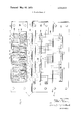
- FIG. 1 is a view in plan illustrating the principal parts of a high speed non-impact, pulsed electrode printer embodying this invention.
- FIG. 2 is a front elevation taken on line 2--2 of FIG. 1.
- FIG. 3 is a side elevation in Section taken on line 3-3 of FIG. 2.
- the printing means comprises an electrode sheet 12 and a terminal sheet 14 in closely adjacent, facing rela-..
- a composite paper web 20 extends from a supply roll 22 'over a curved face of the electrode sheet 12 to a take-up roll 24. These rolls are driven in a conventional manner, preferably at a constant speed bearing a'predetermined relationship to controls for the character selection impulses passing through the several wires 19.
- a flexible metal band 28 isreceived over rolls 30 and held under tension by a spring 32, thereby urging the web 20 with alight pressure against the surface of the sheet 12.
- the band 28 is grounded to the frame of the printer, as illustrated.
- the paper web 20 may be of any suitable type adapted to form a visible or latent image of selected characters when subjected to an electrical field formed by the application of brief electrical pulses between the electrode sheet'lZ and the band 28. While the invention is not primarily concerned with the particular structureof the web 20, an example is illustrated in the drawing for application of the invention to the methods described in the above-identified Haeberle patent.
- This web comprises a donor web 34 and a recipient web 36.
- the donor web 34 may comprise a substrate fabric of cloth material, paper or plastic film, which either comprises or has coated upon it a high resistivity medium upon which printing particles 38-are dispersed.
- These particles are mobile and electrically conductive pigment particles which, in the presence of a brief electrical field pulse, are physically transferred from the donor sheet to the facing surface of the recipient web 36 as described in said patent.
- the web 36 may be any suitable paper upon which the particles may be thus de-v posited to form a visible image.
- the shape of this image depends upon the shape of the applied electrical field which is defined by the shapes of character electrodes on the sheet 12 as hereinafter described. While the webs 34 and 36 are shown in FIG. 3 as being somewhat separated, in practice they are preferably in facing contact, being held in contact by a light pressure appliedby the band 28 or by other means that will permit easy and rapid separation of the webs 34 and 36 after the image transfer has occurred.
- the sheets both have the same basic structure consisting of insulating bases or substrates 40 and 42 of high dielectric material such'as nylon or the equivalent, these substrates being initially coated with a layer of copper or other metallic conductor. Both surfaces of the sheet 14 are so coated, and the non-facing surface of the sheet 12 is thus coated. The copper is selectively etched from the surfaces to leave the residual conductive patterns as hereinafter more fully described.
- the side of the electrode sheet 12 that faces the composite web 20 has a large electrically Conductive marginal surface 44 defininga centraletched region 46 that is non-conductive except for a pattern of electri' cally conductive character-shaped electrodes 48, preferably arranged in a line containingall of the available alphanumeric characters and any other desired punctuation marks, patterns, designs including logotypes, ligatures and symbols to be printed in desired sequences to form a text,'music or other composition, or a formula or any other visible collocation of the availablecharacters.
- the opposite face of the sheet l2 is preferablyuncoated whereby the insulating surface of the base 40 is exposed throughout the area of the sheet 12 facing the sheet 14.
- the electrode sheet 14 has a side 50 facing the sheet 12, this side having a substantial electrically conductive marginal surface 52 defining an etched, 'nonv conductive central region 54 generally aligned with the region 46 on the sheet 12, and also defining nonconductive margins 55.
- the sheet 14 also has 'a side 56, this side having a substantial electrically conductive marginal surface 58 and a plurality of mutually spaced electrically conductive strips 60. These strips, like all of the other electrically conductive surfaces on the sheets
- the strips 60 preferably have eye shaped central end portions 62 and terminal end portions 64. The central portions 62.
- connection wires such as 67 are soldered to the end terminals 64 and extend to the pulse circuits associated with the wires 19.
- An electrical lead wire 68 passes through a drill hole in the base 40 of the sheet 12 (FIG. 3) and is soldered or otherwise electrically connected with the underside of each character electrode 48.
- This wire passes through a corresponding hole 66 in the sheet 14 and is soldered as at 70 to a central end portion 62 of a corresponding strip 60.
- the opposite terminal end portion 64 of this strip comprises terminal means by which the character may be connected through the wire 67 with circuits associated with the leads 19 of FIG. 1.
- the above-described structure also provides means for shielding the respective character electrodes 48 and strips 60 from one another and from spurious externally-generated electrical fields.
- those electrically conductive surface portions of the sheets 12 and 14 that are not electrically connected with the electrodes 48 and strips 60 as above described are connected together and suitably grounded to the control circuit. This may be accomplished in various ways, for example by machine screws or other fasteners passing through holes 72 that also serve for alignment andsupport of the sheets.
- the surface portions 44, 52 and 58 are electrically connected together and grounded.
- each adjacent pair of strips 60 is further increased by the provision of integral spaced extensions 74 of the surface 58, as shown in FIG. 4.
- the surface portion 58 electrically isolates the respective strips 60.
- the strips 60 are often arranged so that alternate strips extend in opposite directions from the central portion of the sheet 14 as shown, thereby providing space for the extensions 74 as above described.
- longitudinally-extending electrically conductive lateral portions 76 of the surface 52 between the non-conductive areas 54 and 55 provide isolation between circuit wires such as 67 and the leads 68 extending between the sheets 12 and 14.
- Printing means comprising sheets 12 and 14 are readily fabricated in the manner hereinabove described, and a given printer may be provided with a large number of pairs of sheets comprising various typographical styles and combinations of selectable printing characters 48.
- Etching techniques employing photographic resists which are well known in the art,
- Prin ting means having, in combination,
- an electrode sheet comprising an insulating base and A a plurality of character-shaped electrodes arranged in a pattern on a surface thereof, said surface having a conductive portion substantially surrounding the region including saidpattem without electricallycontacting said electrodes,
- terminal sheet having a surface facing the other surface of said electrode sheet and comprising an insulating base and a plurality of mutually spaced electrically conductive strips on the non-facing surface thereof, each strip corresponding to an electrode on the first sheet and having a first end and a second end, the first ends of said strips being aligned with said pattern and the second ends having terminal means,
- Printing means having, in combination,
- an electrode sheet comprising an insulating base and a plurality of character-shaped electrodes arranged in a pattern on a surface thereof,
- a terminal sheet having a surface facing the other surface of said electrode sheet and comprising an insulating base, a plurality of mutually spaced electrically conductive strips on the non-facing surface thereof and mutually connected conductive portions extending between said strips, each strip corresponding to an electrode on the first sheet and 1 having a first end and a second end, the first ends of said strips being aligned with said pattern and the second ends having terminal means, and a lead extending through the bases of said sheets and electrically connecting each said electrode with the first end of a corresponding strip. 5.
- the electrodes are etched metallic coatings.
Landscapes
- Physics & Mathematics (AREA)
- General Physics & Mathematics (AREA)
- Printers Or Recording Devices Using Electromagnetic And Radiation Means (AREA)
- Particle Formation And Scattering Control In Inkjet Printers (AREA)
- Dot-Matrix Printers And Others (AREA)
Applications Claiming Priority (1)
| Application Number | Priority Date | Filing Date | Title |
|---|---|---|---|
| US17206771A | 1971-08-16 | 1971-08-16 |
Publications (1)
| Publication Number | Publication Date |
|---|---|
| US3733613A true US3733613A (en) | 1973-05-15 |
Family
ID=22626234
Family Applications (1)
| Application Number | Title | Priority Date | Filing Date |
|---|---|---|---|
| US00172067A Expired - Lifetime US3733613A (en) | 1971-08-16 | 1971-08-16 | Electrode and terminal structure for non-impact printer |
Country Status (9)
| Country | Link |
|---|---|
| US (1) | US3733613A (enExample) |
| JP (1) | JPS4849331A (enExample) |
| BE (1) | BE787496A (enExample) |
| CA (1) | CA940588A (enExample) |
| DE (1) | DE2240308A1 (enExample) |
| FR (1) | FR2150068A5 (enExample) |
| GB (1) | GB1331030A (enExample) |
| IT (1) | IT964005B (enExample) |
| NL (1) | NL7211151A (enExample) |
Cited By (5)
| Publication number | Priority date | Publication date | Assignee | Title |
|---|---|---|---|---|
| US3898674A (en) * | 1973-08-10 | 1975-08-05 | Carter S Ink Co | High resolution non-impact printer |
| US3914771A (en) * | 1973-11-14 | 1975-10-21 | Minnesota Mining & Mfg | Electrographic recording process and apparatus employing synchronized recording pulses |
| US3979758A (en) * | 1973-04-19 | 1976-09-07 | Kilby Jack S | Electrostatic head with toner attracting plates |
| US4176364A (en) * | 1975-09-09 | 1979-11-27 | Sci Systems, Inc. | Grounding device for rotary electrical printer and method |
| US4326458A (en) * | 1979-07-19 | 1982-04-27 | Sign Electronics Limited | Printing apparatus |
Families Citing this family (1)
| Publication number | Priority date | Publication date | Assignee | Title |
|---|---|---|---|---|
| US4237469A (en) * | 1977-12-06 | 1980-12-02 | U.S. Philips Corporation | Electrostatic write head |
Citations (3)
| Publication number | Priority date | Publication date | Assignee | Title |
|---|---|---|---|---|
| US3438052A (en) * | 1965-11-17 | 1969-04-08 | Xerox Corp | Air-supported housing containing tesi printing drum |
| US3453648A (en) * | 1967-08-29 | 1969-07-01 | Milgo Electronic Corp | Thermal printing device |
| US3550153A (en) * | 1967-12-27 | 1970-12-22 | Carter S Ink Co | High speed non-impact printing |
-
1971
- 1971-08-16 US US00172067A patent/US3733613A/en not_active Expired - Lifetime
-
1972
- 1972-08-11 FR FR7229028A patent/FR2150068A5/fr not_active Expired
- 1972-08-11 BE BE787496A patent/BE787496A/xx unknown
- 1972-08-14 IT IT28212/72A patent/IT964005B/it active
- 1972-08-15 CA CA149,480A patent/CA940588A/en not_active Expired
- 1972-08-15 JP JP47081216A patent/JPS4849331A/ja active Pending
- 1972-08-15 GB GB3798472A patent/GB1331030A/en not_active Expired
- 1972-08-16 DE DE2240308A patent/DE2240308A1/de not_active Withdrawn
- 1972-08-16 NL NL7211151A patent/NL7211151A/xx not_active Application Discontinuation
Patent Citations (3)
| Publication number | Priority date | Publication date | Assignee | Title |
|---|---|---|---|---|
| US3438052A (en) * | 1965-11-17 | 1969-04-08 | Xerox Corp | Air-supported housing containing tesi printing drum |
| US3453648A (en) * | 1967-08-29 | 1969-07-01 | Milgo Electronic Corp | Thermal printing device |
| US3550153A (en) * | 1967-12-27 | 1970-12-22 | Carter S Ink Co | High speed non-impact printing |
Cited By (5)
| Publication number | Priority date | Publication date | Assignee | Title |
|---|---|---|---|---|
| US3979758A (en) * | 1973-04-19 | 1976-09-07 | Kilby Jack S | Electrostatic head with toner attracting plates |
| US3898674A (en) * | 1973-08-10 | 1975-08-05 | Carter S Ink Co | High resolution non-impact printer |
| US3914771A (en) * | 1973-11-14 | 1975-10-21 | Minnesota Mining & Mfg | Electrographic recording process and apparatus employing synchronized recording pulses |
| US4176364A (en) * | 1975-09-09 | 1979-11-27 | Sci Systems, Inc. | Grounding device for rotary electrical printer and method |
| US4326458A (en) * | 1979-07-19 | 1982-04-27 | Sign Electronics Limited | Printing apparatus |
Also Published As
| Publication number | Publication date |
|---|---|
| BE787496A (fr) | 1972-12-01 |
| GB1331030A (en) | 1973-09-19 |
| NL7211151A (enExample) | 1973-02-20 |
| DE2240308A1 (de) | 1973-03-01 |
| IT964005B (it) | 1974-01-21 |
| CA940588A (en) | 1974-01-22 |
| FR2150068A5 (enExample) | 1973-03-30 |
| JPS4849331A (enExample) | 1973-07-12 |
Similar Documents
| Publication | Publication Date | Title |
|---|---|---|
| US3718936A (en) | Electrostatic matrix head construction | |
| US2486985A (en) | Electrical printing type | |
| EP0247699B1 (en) | Image-forming element for an electrostatic printer, and a printer in which an element of this kind is used | |
| US4214122A (en) | Resistive planar graphical entry device | |
| US4704621A (en) | Printing device | |
| US4054885A (en) | Electrostatic recording device | |
| DE3779605T2 (de) | Corona-aufladevorrichtung. | |
| US3733613A (en) | Electrode and terminal structure for non-impact printer | |
| US4357618A (en) | Electrostatic imaging apparatus | |
| US2942077A (en) | Electrostatic controls | |
| US4088891A (en) | Electrostatic aperture printing | |
| US3787722A (en) | Printing apparatus | |
| US4123762A (en) | Improved electrostatic head with toner-repelling electrode | |
| US3372400A (en) | Electrostatic recorder with plural electrodes and biased mask | |
| JPS5839674B2 (ja) | セイデンインサツヨウノデンキテキニ マドレスサレル アナアキヘンチヨウキ | |
| US4025927A (en) | Multilayer magnetic image recording head | |
| EP0054406B1 (en) | Writing pad for a character recognition device | |
| US4035812A (en) | Ink jet recorder and charge ring plate therefor with reduced deplating current | |
| US3623123A (en) | Electrostatic printer | |
| US4568946A (en) | Charge electrode means for ink jet printer | |
| US3509816A (en) | Printing arrangement utilizing a continuously moving transfer band | |
| DE1447873B2 (de) | Vorrichtung zum elektrostatischen drucken | |
| US4068585A (en) | Electrostatic printer support with controlled electrostatic surface voltage | |
| US3962969A (en) | Ink mist type high speed printer | |
| JPS5913351B2 (ja) | 静電パ−符号プリンタ |