US3614404A - Electronic calculator - Google Patents
Electronic calculator Download PDFInfo
- Publication number
- US3614404A US3614404A US816965A US3614404DA US3614404A US 3614404 A US3614404 A US 3614404A US 816965 A US816965 A US 816965A US 3614404D A US3614404D A US 3614404DA US 3614404 A US3614404 A US 3614404A
- Authority
- US
- United States
- Prior art keywords
- network
- binary
- output
- multiplier
- digit
- Prior art date
- Legal status (The legal status is an assumption and is not a legal conclusion. Google has not performed a legal analysis and makes no representation as to the accuracy of the status listed.)
- Expired - Lifetime
Links
- 238000010276 construction Methods 0.000 claims abstract description 5
- 238000001514 detection method Methods 0.000 claims description 7
- 230000008878 coupling Effects 0.000 claims description 2
- 238000010168 coupling process Methods 0.000 claims description 2
- 238000005859 coupling reaction Methods 0.000 claims description 2
- 238000000034 method Methods 0.000 abstract description 9
- 238000012937 correction Methods 0.000 abstract description 6
- 238000013461 design Methods 0.000 abstract description 4
- 238000012986 modification Methods 0.000 abstract description 2
- 230000004048 modification Effects 0.000 abstract description 2
- 239000004065 semiconductor Substances 0.000 abstract 1
- 230000000295 complement effect Effects 0.000 description 39
- 238000010586 diagram Methods 0.000 description 26
- 239000011159 matrix material Substances 0.000 description 17
- 230000004044 response Effects 0.000 description 11
- 230000000881 depressing effect Effects 0.000 description 7
- 230000008569 process Effects 0.000 description 7
- 230000000994 depressogenic effect Effects 0.000 description 6
- 238000007620 mathematical function Methods 0.000 description 6
- 238000012546 transfer Methods 0.000 description 5
- VSGPGYWZVPDDSK-UHFFFAOYSA-N 2-(5-methoxy-2-phenyl-1h-indol-3-yl)-n,n-dimethylethanamine Chemical compound CN(C)CCC=1C2=CC(OC)=CC=C2NC=1C1=CC=CC=C1 VSGPGYWZVPDDSK-UHFFFAOYSA-N 0.000 description 3
- 230000000977 initiatory effect Effects 0.000 description 3
- ZCJJIQHVZCFSGZ-UHFFFAOYSA-N 2,8-bis(diphenylphosphoryl)dibenzothiophene Chemical compound C=1C=CC=CC=1P(C=1C=C2C3=CC(=CC=C3SC2=CC=1)P(=O)(C=1C=CC=CC=1)C=1C=CC=CC=1)(=O)C1=CC=CC=C1 ZCJJIQHVZCFSGZ-UHFFFAOYSA-N 0.000 description 2
- 238000012804 iterative process Methods 0.000 description 2
- 239000013642 negative control Substances 0.000 description 2
- 238000004364 calculation method Methods 0.000 description 1
- 230000002860 competitive effect Effects 0.000 description 1
- 239000013256 coordination polymer Substances 0.000 description 1
- 230000003467 diminishing effect Effects 0.000 description 1
- 230000009977 dual effect Effects 0.000 description 1
- 230000000694 effects Effects 0.000 description 1
- VIKNJXKGJWUCNN-XGXHKTLJSA-N norethisterone Chemical group O=C1CC[C@@H]2[C@H]3CC[C@](C)([C@](CC4)(O)C#C)[C@@H]4[C@@H]3CCC2=C1 VIKNJXKGJWUCNN-XGXHKTLJSA-N 0.000 description 1
- 238000012545 processing Methods 0.000 description 1
- 230000000007 visual effect Effects 0.000 description 1
Images
Classifications
-
- G—PHYSICS
- G06—COMPUTING; CALCULATING OR COUNTING
- G06F—ELECTRIC DIGITAL DATA PROCESSING
- G06F7/00—Methods or arrangements for processing data by operating upon the order or content of the data handled
- G06F7/38—Methods or arrangements for performing computations using exclusively denominational number representation, e.g. using binary, ternary, decimal representation
- G06F7/48—Methods or arrangements for performing computations using exclusively denominational number representation, e.g. using binary, ternary, decimal representation using non-contact-making devices, e.g. tube, solid state device; using unspecified devices
- G06F7/491—Computations with decimal numbers radix 12 or 20.
- G06F7/4915—Multiplying; Dividing
- G06F7/4917—Dividing
Definitions
- FIG. 4 presents a series of graphs employed in a description of the invention relating to addition and subtraction
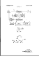
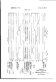
- FIG. 1 illustrates a general block diagram of a manually operated electronic calculator which broadly sets forth the major components of the present system and their functional relationship to one another.
- a keyboard panel I including a IO-key keyboard 2 for entering multidigit numbers into the machine and a function selector 3 for detennining various functions to be performed.
- the keyboard 2 is coupled to a decimal to binary-coded decimal converter 4 which is in turn coupled to a dual storage stage 5.
- a key display 6 indicates the most recently stored number.
- the output of the stage 5 is coupled to computational circuitry 7 which includes an adder-subtracter stage 8 and a multiplier-divider stage 9.
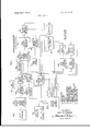
- the multiple-pole, double-throw switch network 123 includes doublepole, double-throw switchs 230,
- error sensor network 126 The true output from each of the higher order three addersubtracter components 241, 242 and 243, the true and complementary carry (borrow) outputs of the highest order adder subtracter component 243, and add and subtract control signals from logic network 110 are connected to error sensor network 126.
- This network is schematically illustrated in FIG. 11, to be considered presently.
- the output of error sensor net work 126 is applied to each of the DP'D'I switches 230 through 237 for gang connecting said switches into their second positions in response to an uncorrected output from the full addemubtracter network 124.
- a source 505 for storing the BCD number five is coupled as the second input to comparator network 502 t'or making a comparison with the most significant digit of the divisor R. For most significant digits less than five a signal is applied to the multiplier circuit 503 for causing it to multiply both the divisor R and the dividend Z by two, which products are fed back to the storage networks 500 and 501. A second comparison is then made in the comparator network 502 and if the most significant digit is still less than five the multiplication process is repeated. When the most significant digit exceeds 5 the modified divisor R is coupled as a first input to a multiplier circuit 506.
Landscapes
- Engineering & Computer Science (AREA)
- Computing Systems (AREA)
- Physics & Mathematics (AREA)
- General Physics & Mathematics (AREA)
- Theoretical Computer Science (AREA)
- Computational Mathematics (AREA)
- Mathematical Analysis (AREA)
- Mathematical Optimization (AREA)
- Pure & Applied Mathematics (AREA)
- General Engineering & Computer Science (AREA)
- Complex Calculations (AREA)
Abstract
An inexpensively fabricated electronic calculator for efficiently performing basic mathematical operations including addition, subtraction, multiplication and division is disclosed. In the multiplication operation binary coded numbers are transformed into a unary code using a serial, digit-by-digit technique. A logical design is employed which permits a circuit construction utilizing relatively inexpensive semiconductor devices, specifically of an integrated circuit MOSFET design. In addition and subtraction operations binary-coded decimals are employed throughout, with correction of uncorrected sums being made by suitable modifications of the circuit which permit the adder-subtracter network per se to be traversed twice thereby obviating the need for a separate correction network. A division operation is performed employing multiplication and additionsubtraction circuitry.
Description
United States Patent [111 3,
[72] Inventor Mark M.Garfein 3,508,037 4/1970 Collins et a1. 235/159 Dewitt,N.Y. 3,513,303 5/1970 Kitz et a1 235/160 [21] fi i 1969 Primary Examiner--Mzilcolm A. Morrison Pai s 19 1971 Assistant Examiner-Charles E, Atkinson 1 I Attorneys Marvin A, Goldenberg, Richard V. Lang, Frank L. [73} Assignee General Electric Company Neuhauser and Oscar B wadde [54] ELECTRONIC CALCULATOR 5 Claims 13 Drawing Figs ABSTRACT: An inexpensively fabricated electronic calcula tor for efficiently performing basic mathematical operations [52] U.S.Cl 235/159 induding addition Subtraction, multiplication and division is 235/168, 235/174 disclosed In the multiplication operation binary coded num- [51] Int. Cl G06! 7/48 hers am transformed into a unary code using a Serial di ipb [50] Field of Search 7. 235/156, digit technique. A logical design is employed which permits a 173, [74, 150-3 circuit construction utilizing relatively inexpensive semicond ductor devices, specifically of an integrated circuit MOSFET References design. In addition and subtraction operations binarycoded UNITED STATES PATENTS decimals are employed throughout, with correction of uncor- 2,928,601 3/1960 Curtis... 235/169 X rected sums being made by suitable modifications of the cir- 3,112,396 11/1963 Heywood 235/170 cuit which permit the adder-subtracter network per se to be 3,278,734 /1966 Ulbrich et al.. 235/174 X traversed twice thereby obviating the need for a separate cor- 3,304,418 2/ 1967 Perrotto et a1. 235/169 rection network A division operation is performed employing 3,460,129 8/1969 Thorvaldsson 235/1503 multiplication and addition-subtraction circuitry.
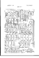
|oe- E 1oz |o4 DISPLAY ADDER a SUBTRACTER oecmm. I 1 2 1 mm" ROTARY PREGATE x V 1 STORAGE SWITCH NETWORK MULTIPLE newsman CODE usrwonx NETWORK POLE FULL r i DECIMAL DOUBLE ADDER ROTARY 1 CONVERTER 1 meow *1 suarancrss l ISS 1 7D|GlT ROTARY SWITCH NETWORK STORAGE SWlTCH NETWORK L msrwonx nerwenx 1 F '26; P ..l.. 1 5C0 senor; I 095" SENSO FUNCTION 1 SELECTOR Lc J lNHlBlT ADD HULTIPLY A GATE 'sunucr mm: g NETWORK m 0 ..Q"'T".:':L:- M-
1 a F G t l P 2 1 533531 new 2 MASTER I m CONTROL 1 LOGIC NETWORK j! I! J J lso 12,1 A-ENTERE ADO 8CD ZERO B-SUBTRACT DOWN DETECTOR 33. 1195 COUNTER MULTIPLIER E- SWlTCH 12o CONTROL 151 f 132 F AODlSUBT) CONTROL 6 'SWITCH I28 CONTROL 8CD ROTQRY time; eases .1 RATE MULTIPLIER CLOCK MULTIPUER K" SWITCH I32 CONTROL J L ZERO DETECTION PAIENTEuom 19 Ian 3. 6 1 4.404
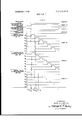
MASTER CONTROL STAGE LOGIC NETWORK r" ia' gE I I0 KEY FUNCTION CONVERTER l KEYBOARD SELM-E'JOR L a J FIGS V INVENTOR:
MARK M. GARFEIN,
BYW
HIS ATTORNEY.
PATENTEDUET 19 ml 3, 14,404
SHEET u [If 7 ENTER a ADD FIGA PULSE l GRAPH A ADD CONTROL PULSE T0 PRE-GATE I228 I GRAPH B season 126 1 sun CONTROL PULSE T0 PRE-GATE I22 8 I RAP SENSORIZG r- G H C CONTROL PULSE CONTROL PULSES TO SWITCH unmxss GI TO mmamu 1 GRAPH D G4 m GRAPH E CONTROL PULSES To swncH HATRIXES 6 1 I G n GRAPH F l l m Hum {I} T a Hu 7 a INVENTOR MARK M. GARFEIN,
HIS ATTORNEY PATENTEnnm 19 um 3.614.404 SijEET 70F 7 FIGJZ F|G.l3 50? l ecu N0 STORAGE 4 3 NETWORK 508 an MULTIPLIER DELAY 50 CIRCUIT MULTIPLIER SUBTRACT j CIRCUIT CIRCUIT GATE 'Ebfi ouonem z 504 505 5025 8CD COMPARATOR MULTIPLIER -0.5 NETWORK CIRCUIT T SCI] 9 l STORAGE STORAGE NETWORK NETWORK DIVISOR R DIVIDEND!- INVENTORI MARK M. GARFEIN,
HIS ATTORNEY.
ELECTRONIC CALCULATOR BACKGROUND OF THE INVENTION l. Field of the Invention The invention relates to the field of low-cost electronic cal culators designed to perform basic mathematical functions, in particular to electronic desk top calculators.
2. Description of the Prior Art The past several years has been the advent of small totally electronic calculators designed to perform basic mathematical functions. These machines are intended to replace mechanical and and electromechanical desk calculators, holding the principal advantages of speed, weight, quiet operation and, potentially, cost. The electronic machines developed to date are essentially small, special purpose computers designed along the lines of large scale computers, including appreciable storage capacity and employing numerous high-speed devices. Thus, presently available electronic calculators are not found to be competitive on a cost basis with the older form of machines. The present invention introduces innovations into the circuitry of the electronic calculator so as to appreciably reduce its cost.
SUMMARY OF THE INVENTION It is a principal object of the invention to provide a novel electronic calculator capable of accurately performing basic mathematical functions which can be fabricated at costs substantially reduced relative to presently available electronic calculators.
It is another object of the invention to provide a novel elec tronic calculator which has reduced hardware requirements.
It is a further object of the invention to introduce novel computing techniques to an electronic calculator as above described which make possible the employment of inexpensive batch-fabricated circuitry, in particular MOSFET integrated circuits.
Another object of the invention is to provide a novel electronic calculator as above described which implements simplified logic for obtaining product and quotient outputs.
It is yet another object of the invention to provide a novel electronic calculator as described which in performing addition-subtraction operations obviates the need for a separate correction network.
These and other objects are accomplished in accordance with one embodiment of the invention for performing multiplication of two binary-coded decimal numbers by a circuit which includes a binarycoded decimal counter into which the binary bits of the multiplicand are entered in a first digital sequence. There is further provided a binary'coded decimal rate multiplier having applied thereto in a second digital sequence the binary bits of the multiplier, said rate multiplier generating during a given period unary pulses which correspond in number to the quantity of the applied digit. The generated unary pulses are accumulated in an output accurnulater. At the end of each given period the counter containing the multiplicand is caused to reduce its count by one. Upon reaching zero, generation of said unary pulses is terminated so that the accumulated pulses correspond to the product of digits applied to said decimal counter and rate multiplier.
In accordance with a further embodiment of the invention an addition and subtraction operation of two binary-coded decimal numbers is performed by a circuit which includes an adder-subtracter network to first and second inputs of which the binary bits of the first and second numbers are connected in digital sequence. An error sensor network responsive to the output of said adder-subtracter network generates an error signal in response to an incorrect output. The error signal is employed to switch the incorrect output back to said first in puts and to connect a correction constant to said second inputs, thereby providing a corrected output.
In accordance with yet another embodiment of the invention a division operation of two binary-coded decimal numbers is performed by a circuit which includes multiplier and addition-subtraction components as described above. The reciprocal of the divisor is obtained through an iterative process. The quotient is generated by multiplying the reciprocal quantity by the dividend.
BRIEF DESCRIPTION OF THE DRAWING best understood from the description of the preferred embodiments, taken in connection with the accompanying drawings in which:
FIG. 1 is a general block diagram of an electronic calculator in accordance with the present invention;
FIG. 2 is a functional block diagram of the electronic calculator of FIG. 1-,
FIG. 3 is the more detailed schematic block diagram of the present electronic calculator, conforming to the diagram of FIG. 2;
FIG. 4 presents a series of graphs employed in a description of the invention relating to addition and subtraction;
FIG. 5 presents a series of graphs employed in a description of the invention relating to multiplication;
FIG. 6 is a schematic circuit diagram of a simple MOSFET singlepole, single-throw switch used prominently in the present circuit;
FIG. 7 is a schematic circuit diagram of a singlerotary switch matrix of FIG. 3;
FIG. 8 is a schematic circuit diagram of a singleMOSFET NAND gate used prominently in the present circuit;
FIG. 9 is a schematic circuit diagram of a pregate component of FIG. 3;
FIG. 10 is a schematic circuit diagram of a full adder-subtracter component of FIG. 3;
FIG. 11 is a schematic circuit diagram of the error sensor network shown in FIGS. 2 and 3;
FIG. 12 is a schematic circuit diagram of the binary-coded decimal rate multiplier shown in FIGS. 2 and 3; and
FIG. 13 is a functional block diagram illustrating a division operation employing multiplication and addition'subtraction circuitry shown in FIGS. 2 and 3.
DESCRIPTION OF THE PREFERRED EMBODIMENTS FIG. 1 illustrates a general block diagram of a manually operated electronic calculator which broadly sets forth the major components of the present system and their functional relationship to one another. Represented are a keyboard panel I including a IO-key keyboard 2 for entering multidigit numbers into the machine and a function selector 3 for detennining various functions to be performed. The keyboard 2 is coupled to a decimal to binary-coded decimal converter 4 which is in turn coupled to a dual storage stage 5. A key display 6 indicates the most recently stored number. The output of the stage 5 is coupled to computational circuitry 7 which includes an adder-subtracter stage 8 and a multiplier-divider stage 9. Although shown as two separate stages, for a division operation it will be seen that these blocks become interrelated and share common components. The function selector 3 is coupled to a master control logic network 10, in turn coupled to the computational circuitry 7. A further connection is provided between logic network 10 and storage stage 5. The output of the circuitry 7 is coupled to an accumulator network 11 and is displayed by display 12. A feedback connection is provided from the accumulator 11 to the storage stage 5.
Decimal numbers are manually entered into the machine through the keyboard 2. The function selector 3 may include a number of keys for selecting the mathematical functions to be performed as well as other conventional functions in the operation of such a machine such as ON, OFF, CLEAR and ERROR. Briefly, an operational sequence is as follows: (I)
Enter a first number into the keyboard 2. This number is instantaneously stored in one-half of the stage and appears in the key display 6. (2) Depress the ENTER & ADD key of the function selector 3, which triggers the logic network and causes the number stored in stage 5 to be added to the previously accumulated output. When the previous output is 0" the effect is to shift the number into the accumulator 11. (3) Enter a second number into the keyboard 2. (4) Depress the function selector 3 key of the function to be performed. In response thereto the logic network 10 generates a sequence of the control signals for performing the selected mathematical function, the resulting quantity being stored in the accumulator and appearing in the display 12.
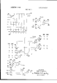
Shown in FIG. 2 is a functional block diagram of the addersubtracter and multiplier circuitry of the present system. Blocks corresponding to those of FIG. 1 have similar reference characters, but elevated to the 100 series. It is noted that the functional lines coupled to logic network 110 are identified by letters, and the various signals transmitted along these lines are listed in FIG. 2. Function selector 103 is coupled to master control logic network 110 by control line A, B, C, D for initiating addition, subtraction, multiplication and division operations, the block diagram for division being illustrated in FIG. 13. The IO-key keyboard 102 is connected through a decimal to binary-coded decimal converter 104 to a first storage network 120. The network 120 stores seven binary-coded decimal digits, each digit comprising four binary bits. Key display 106 provides a visual indication of the number stored in the network 120. For addition-subtraction, a
Considering now the multiplication circuitry, the output of the rotary switch network 121 is further connected to a binary-coded decimal down counter 130. The output of rotary switch network 129 is further connected to a binary-coded decimal rate multiplier 131. Also connected to rate multiplier 131 is a clock signal from logic network 110 transmitted on control line J. The rate multiplier 131 generates unary pulses at its output from which the product quantity is obtained. The unary pulses are sequentially connected through a rotary switch matrix 132, governed by control line K, to the accumulator 111. It also provides a trigger to the BCD down counter 130 for actuating this device. The BCD down counter 130 is coupled to a zero detector 133 which detects a zero condition of the counter and couples this information back to the master control logic network for arresting the clock signals and actuating switch networks 120, 128 and 132.
In FIG. 3 the adder-subtracte'r and multiplier circuitry is shown in still greater detail in a schematic functional diagram. The blocks of FIG. 3 that are the same as those of FIG. 2 are identified by identical reference characters.
The lO-key keyboard 102 is a conventional component integrally connected with the decimal to binary-coded decimal converter 104. The keyboard includes 10 single-pole, doublethrow switches 200 representing decimal digits zero through none. The switches 200 are schematically shown as electromechanical switches, although in practice they may be electronic touch responsive devices. First fixed terminals of said switches are joined together and connected through a current limiting resistor 201 to ground, and second fixed terminals are connected to ground. The movable contacts of switches 200 are each connected through a bias resistor 202 to a negative voltage source -V,. The movable contacts are further connected to four NAND- gates 203, 204, 205 and 206, the outputs of which represent, respectively, four binary bit orders :18, a1, a2 and m4 of the binary-coded decimal number. The encoding function is performed by appropriate connections from the switches 200 to the NAND-gates 203 through 206. Specifically, switches eight and nine provide inputs to gate 203, switches nine, one, three, five and seven provide inputs to gate 204, switches three, seven, two and six provide inputs to gate 205; and switches five, seven, six and four provide inputs to gate 206. A pulse generator 209 is connected from resistor 201 to storage network for shifting the stages thereof.
The storage network 120 includes four seven- stage registers 210, 211, 212 and 213 for storing, respectively, the binary bits al, a2, a4 and 0:8 for each digit d, through d,. These bits are connected to the first stages of the registers from the corresponding NAND gates of the converter 104 and shifted each time a digit is entered into the keyboard.
The binary switch network 121 includes four identically constructed seven-input rotary switch matrixes 214, 215, 216 and 217, one switch matrix for each binary bit. The inputs of each switch matrix correspond to the digit stages of the associated storage register. Thus, the output of each stage of storage register 210 is connected to a corresponding input of rotary switch matrix 214. Similarly, registers 21], 212 and 213 are connected to rotary switch matrixes 215, 216 and 217, respectively. Control signals are connected from the master control logic network 110 jointly to control terminals G through G, of the rotary switch matrixes so as to switch in parallel the binary bits of a single-decimal digit, the switching being accomplished in sequence with respect to each digit. A schematic diagram of a single seven-input rotary switch matrix is shown in FIG. 7 and will be considered in grater detail subsequently.
The pregate network 122 includes four pregate components 218, 219, 220 and 221. The output of rotary switch 214 is directly connected as a true signal X to pregate component 218 and as a complementary signal K through an inverter 222.
Similarly, converters 223, 224 and 225 are coupled at the out-* puts of switches 215, 216 and 217 for supplying true and complementary signals to components 219, 220 and 221. In addition, the pregate components have add and subtract control signals applied from the master control logic network 110. The pregate components are each identical and one such component is schematically illustrated in FIG. 9, to be discussed presently.
As illustrated, the multiple-pole, double-throw switch network 123 includes doublepole, double-throw switchs 230,
231, 232, 233, 234, 235, 236 and 237, operatively ganged together. Full adder-subtracter network 124 includes four similar full adder- subtracter components 240, 241, 242 and 243, for one of which is the schematic circuit diagram of FIG. 10. In one position the switch 230 connects true and complementary outputs from pregate components 218 as a first pair of inputs X and Y to full adder-subtracter component 240. In its second position the switch 230 connects true and complementary outputs of the full adder-subtracter component 240 back to its first pair of inputs. Similar connections are provided by switches 231, 232 and 233 between pregate components 219, 220 and 221 and their corresponding adder- subtracter components 241, 242 and 243.
The output of rotary switch matrix 248 is connected as true and complementary signals to a first pair of fixed terminals of double-pole, double-throw switch 234, the complementary signal being derived by means of an inverter 252. A second pair of fixed terminals is connected to a source 256 generating a binary 0. In one position the moving contacts of switch 234 connect the true and complementary signals from rotary switch matrix 248 to a second pair of inputs Y and Y of full adder-subtracter component 240, and in the second position connect the true and complementary signals representing a 0 binary bit to said second pair of inputs. Similarly, inverters 253, 254 and 255 derive true and complementary signals from the output of switch matrixes 249, 250 and 251, these signals being coupled to first pairs of fixed terminals of switches 235, 236 and 237, respectively. Switches 235, 236 and 237 connect true and complementary signals from switch matrixes 249, 250 and 251 to inputs Y and T of adder- subtracter components 241, 242 and 243, respectively, when in one position. In the second position they connect true and complementary signals representing binary l," l" andf0" from sources 257, 258 and 259, respectively, to the second pair of inputs of components 241, 242 and 243.
True and complementary carry outputs, or borrow outputs in subtract operations, are connected from the three lower order adder- subtracter components 240, 241 and 242 as a third pair of inputs to the next higher order adder-subtracter component. True and complementary carry (borrow) outputs from the highest order adder-subtracter component 243 are connected through a buffer register 264 to the third pair of inputs of the lowest order adder-subtracter component 240. This connection serves to apply a carry (borrow) signal from a given digit to the next higher digit in a sequential manner.
The true output from each of the higher order three addersubtracter components 241, 242 and 243, the true and complementary carry (borrow) outputs of the highest order adder subtracter component 243, and add and subtract control signals from logic network 110 are connected to error sensor network 126. This network is schematically illustrated in FIG. 11, to be considered presently. The output of error sensor net work 126 is applied to each of the DP'D'I switches 230 through 237 for gang connecting said switches into their second positions in response to an uncorrected output from the full addemubtracter network 124.
Rotary switch network includes four seven-output rotary switch matrixes 260, 261, 262 and 263, one for each binary bit, which are of similar construction to the switches of networks 121 and 129. Applied to the switches 260 through 263 as single inputs are the true output signals from corresponding adder-subtracter components 240 through 243.
The accumulator network 111 comprises four l4- stage registers 265, 266, 267 and 268 which provide a storage function for addition and subtraction operations. For multiplication operations, registers 265 through 268 operate as binarycoded decimal counter stages for providing a counting function. The outputs of rotary switch matrix 260 are connected to the first seven stages of the register 265. Similarly, the outputs of rotary switch matrixes 261, 262 and 263 are connected to the first seven stages of corresponding registers 266, 267 and 268. in response to signals from the master control logic network 110 to control terminals G through G, of switch matrixes 260 through 263, the four hits of a given digit are concurrently switched into corresponding registers 265 through 268, the switching being in sequence with respect to successive digits. Outputs of the first seven stages of registers 265, 266, 267 and 268 are connected through inhibit gate network 134 to corresponding stages of the registers 244, 245, 246 and 247, respectively, of network 128.
With respect to the multiplication circuitry, the outputs of rotary switch matrixes 214, 215, 216 and 217 are further con nected in parallel to corresponding four stages of binarycoded decimal down counter 130, the outputs from each of the counter stages being connected to zero detector 133. The outputs of rotary switch matrixes 248, 249, 250 and 251 are further connected in parallel to the binary-coded rate multiplier 131 which is further provided with a clock signal from logic network 110. A schematic diagram of the BCD rate multiplier is shown in FIG. 12 to be described presently. The principal output from BCD rate multiplier 131 is connected through a 14 output rotary switch matrix 132 to each of the i4 stages of the accumulator register 265 for counting up and storing the unary pulses generated by the rate multiplier 131. A secondary output from BCD rate multiplier output 131 generating a trigger signal is connected to BCD down counter for causing the counter to count down. 1
Considering the operation of the system of FIG. 3, an exemplary addition of two multidigit decimal numbers will be described. Normally, a CLEAR key on the keyboard panel is first actuated for clearing the accumulator resistors of any stored data. The first number to be added, the augend, is entered into the calculator by depressing the appropriate digit keys on the keyboard 102, the digits being entered in sequence, the most significant digit first. For example, if the most significant digit is one, depressing the ONE key removes the movable contact from the ground position and closes the circuit to the resistor 201. There is thus applied a negative potential, corresponding to a logic "0," to the input of NAND- gate 204, generating a logic l at its output, which is connected to the first stage of register 210. The remaining NANlD-gates 205, 206 and 203 have entirely logic l's" applied to their inputs and each generate logic 0's" at the out' put, which are coupled to the first stages of registers 211, 212 and 213, respectively. A first decimal digit of "1 is now stored in the first stages. if the second most significant digit is seven, depressing the SEVEN key first causes a shift pulse to be generated from generator 209, which is applied to each stage of the storage registers 210, 211, 212 and 213 for shifting the binary bits of the first applied digit into the second stages of said registers, leaving the first stages cleared. Actuating the 7 switch also generates a logic l at the output of HAND-gates 204, 205 and 206 and a logic 0" at the output of gate 203. HAND- gates 204, 205, 203 and 206 are coupled to the first stages of registers 210, 211, 212 and 213, and the second decimal digit is stored. The remaining digits are sequentially entered in a similar fashion, a shift pulse being generated each time for shifting the previously entered digits and clearing the first stage for acceptance of a new digit.
Next, the ENTER & ADD key is depressed, transmitting a narrow pulse to the master control logic network- 110 in response to which the logic network generates an add sequence of control pulses. Referring to the timing diagram of FIG. 4, the enter and add pulse is shown in Graph A and occurs at time t,. During this add sequence, the first number entered which is stored as a binary-coded decimal in network 120 is added to the binary-coded decimal number stored in the accumulator network 111. The number in network 111 is transferred into the storage network 128 at the beginning of the add sequence, the new sum being stored in the accumulator network. Since for the first add sequence, the first entered number is added to zero, which is the number stored in the accumulator register, this sequence of the operation effectively transfers the augend from the storage network 120 to the accumulator network 111.
The addend is then entered by appropriately depressing the keyboard 102 which places the addend into the storage registers 210 through 213, as previously described. The ENTER & ADD key is again depressed which commences the add sequence for adding the addend to the augend. In response to the enter and add pulse, the logic network 110 first generates add and subtract-control pulses shown in GRaphs B and C, respectively. The add and subtract control pulses are applied to each of the pregate components 218 through 221 and to error sensor network 126. These pulses commence at time t, and extend over a complete add sequence to time T. At time t inhibit control pulses shown in Graph D are also applied to the inhibit gate network 134 for transferring the data stored in the accumulator registers 265, 266, 267 and 268 into the storage registers 244, 245, 246 and 247, respectively. Control pulses commencing at time t, and extending to 1,, shown in Graphs E and F, are then applied simultaneously to control lines G of rotary switch matrixes 214 through 217 and 248 through 251. These control pulses close the switches to which they are applied so as to empty the binary bits of the first digits from the first stages of storage registers 210 through 213 and 244 through 247. From t, to t, constitutes a first-digit period in which the binary bits of the first digits are added to each other. The bits from registers 210 through 213 are each transformed into a true and complementary signal and applied to respective pregate components 218 through 221. The pregate components process the applied data to accommodate either an add or subtract operation in the full adder-subtracter network 124. Accordingly, the data will appear at the appropriate output terminals of the pregate components pursuant to an add operation. (it is noted that for a subtract operation a one s complement is provided and the data appears at the output of the pregate components in an inverted condition.) The pregate data is coupled through DPDT switch components 230-233 to the X and Y inputs of full adder-subtracter components 240 through 243. Correspondingly, the bits from registers 244 through 247 are transformed into true and complementary signals and applied through DPDT sw i tch components 234 through 237 and applied to the Y and Y inputs of full adder-subtracter components 241-243. There are also carry signals supplied to components 241 through 243 from next lower order components. The buffer register 264 receives the carry output from component 243 to be applied to the component 240 during the succeeding digit sequence.
Addition is performed in each of the full adder-subtractor components in two phases extending over the period I, to 1,. During the first phase, uncorrected sums may appear at the outputs of full adder- subtracter components 240 and 243. The uncorrected outputs applied to error sensor network 126 cause a control signal to be generated by network 126 which actuates in parallel switches 230 through 237. Switches 230 through 233 apply the true and complementary uncorrected outputs of the full adder-subtracter components back to the X and 3( input terminals thereof. Switches 234 through 237 apply true and complementary signals of the binary-coded decimal number six to the Y and Y terminals of the full addersubtracter components. During the second phase the new in- Immediately prior to at time I control pulses, shown in Graph G are applied simultaneously to control lines G of rotary switch matrixes 260 through 263 for closing the associated switches and entering the corrected sums of the first digits from adder-subtracter components 240 through 243 into the first stages of the corresponding accumulator registers 265 through 268. If a correct sum appears at the output of the adder-subtracter components during the first phase, a control signal is not generated by the error sensor network 126 and this sum is switched at 1 to the accumulator registers.
In the next digit period of the operation, there is performed addition of the binary bits of the second digits of the stored binary-coded decimal numbers together with a carry that may have been generated in the first digit addition. Accordingly, between times t, and a, control pulses, shown in Graphs E and F, are applied simultaneously to control lines G of the rotary switches 214 through 217 and 248 through 251. Actuation of the associated switches empty the binary bits of the second digits from the second stages of storage registers 210 through 213 and 244 through 247. Once again true and complementary signals are obtained from the output of pregate components 214 through 217 and applied to the X and Y inputs of addersubtracter components 240 through 243, and true and complementary outputs from rotary switches 248 through 251 are applied to the Y and Y inputs of said adder-subtracter components. Uncorrected sum outputs are given correction as previously described. At time t, control pulses are applied to control lines G, of rotary switch matrixes 260 through 263 for entering the corrected sums to the second stages of the accumulator register 265 through 268. The addition operation continues in a digit-by-digit sequence in the manner above described until each of the stages of the storage registers have been emptied and the corrected sums are entered in the accumulator registers. A single addition or subtraction operation for a maximum of two seven-digit numbers may be performed within several milliseconds.
Further addition operations for adding to the previously obtained sums may be readily performed as above described by sequentially entering the numbers to be further added and depressing the ENTER 8!. ADD key for each addition operation.
A subtraction operation is performed in identical fashion to the addition operation and will be only briefly discussed. As with respect to an addition operation, the first number, the minuend, is entered and stored in the storage network 120 by depressing the appropriate keys of the keyboard 102. The ENTER & ADD key is then depressed which transfers the minuend from the storage network 120 into the storage network 128. The subtrahend is then entered by depressing the keyboard. Following this a SUBTRACT key of the function selector 103 is depressed which applies a subtract signal to master control logic network for generating a subtract sequence. The subtract sequence is identical to the add sequence except that the add and subtract control pulses of Graphs B and C of FIG. 4 to pregate network 122 and error sensor 126 are now inverted. The interconnections between the pregate network 122 and the full adder-subtracter network 124 and the connections from network 124 to error sensor network 126 automatically provide in response to the subtract control signal, a subtract operation performed exactly as with respect to the addition operation. With regard to a subtract operation it may be appreciated that the carry signal of the addition operation becomes a borrow signal for subtraction.
For a multiplication operation of two multidigit numbers, the multiplicand is entered into the keyboard 102 and becomes stored in the registers 210 through 213 in the manner previously described. The ENTER & ADD key is then depressed which transfers the multiplicand from storage netmultiply pulse is seen to occur work 120 into the accumulator network 11 1. The multiplier is then entered into the keyboard 102 which stores the multiplier in storage network 120. Next, the MULTIPLY key is depressed which generates a multiply signal that is applied to the master control logic network 110 for commencing the multiply sequence. Referring to Graph A of FIG. a narrow at time t,. in response to the multiply pulse, the logic network 110 generates a narrow control pulse at time t, that is applied to inhibit gate network 134 for transferring the multiplicand from the accumulator network 111 into the storage network 128. This pulse is shown in Graph B. Also at time r a narrow control pulse is simultaneously applied to control lines G, of rotary switches 214 through 217, shown in Graph C. The switches to which the control pulses are applied close and transfer the binary bits of the first digit from the first stages of storage registers 210 through 213 into the binary-coded decimal down counter 130. Commencing at time I, control pulses are applied to control lines G, of rotary switches 248 through 251, as shown in Graph D, for applying the binary bits of the first digit from the first stages of storage registers 244 through 247 to the BCD rate multiplier 131. Also commencing at time r, cloclt pulses at a given frequency j" are applied to the BCD rate multiplier 131 from the logic network 1 10, shown in Graph E.
The BCD rate multiplier comprises a binary counter which for one counting period At==Nlf provides a count of N. During At the BCD rate multiplier gates out a discrete number of unary pulses, shown in Graph F the number being a function of the digit quantity applied form storage registers 244 through 247. Commencing at time i there is a further control pulse applied from the logic network 110 to the control line G, of the rotary switch matrix 132, shown in Graph H, for entering the generated unary pulses into the first stage of the accumulator register 265. In addition to providing a storage function, storage registers 265, 266, 267 and 268 are connected to function as a decade counter. At the end of each period At, a pulse, shown in Graph G, is applied from the BCD rate multiplier 131 to the BCD down counter 130 for counting down by one unit. Upon the counter 130 being counted down to zero, its state is detected by the zero detector network 133 and a pulse is generated at time t,, shown in Graph 1. In response to the pulse from zero detector network 133, logic network 110 terminates the control pulses to control lines G, of switches 248 through 251 and to the control line G, of switch 132, and also gates off the clock pulse to the BCD rate multiplier.
At time 1 control pulses are again applied to the control lines G, of switches 214 through 217, shown in Graph C, for reentering the first digit bits into BCD down counter 130. Commencing at time I control pulses are applied to the con trol lines G, of rotary switches 248 through 251, shown in Graph D, for applying the binary bits of the second digit of storage registers 244 through 247 to the BCD rate multiplier. Commencing at time I, there are also applied control pulses to control line G, of the rotary switch 132, shown in Graph H, and clock pulses to the multiplier 131, shown in Graph E. The rotary switch 132 now connects the unary pulses generated by the BCD rate multiplier to the second stage of register 265. lt is noted there are illustrated fewer output pulses from multiplier 131 during this digit sequence than the first, indicating the digit stored in the second stages of registers 244 through 247 to be of lower value than the digit stored in the first stages. Upon the down counter 130 again reaching a zero count, the zero detection network 133 applies a control pulse to the logic network 110 and the process is repeated. This process con tinues until all seven stages of the storage registers 244 through 247 are sequentially applied to the BCD rate multiplier 131.
In the next sequence of operation, at time I, control pulses are simultaneously applied to control lines G, of rotary switches 214 through 217, shown in Graph C, for entering the binary bits of the second digit stored in registers 210 through 213 into the BCD down counter 130. Commencing at time I, control pulses are simultaneously applied to the control lines G, of switches 248 through 251 for applying the binary bits of the first digit stored in registers 244 through 247 to the BCD rate multiplier, shown in Graph D. Commencing at this time t, there are also clock pulses applied to the BCD rate multiplier, Graph E, and control pulses applied to control line G, of the rotary switch 132, shown in Graph H. Thus, the unary pulsesgenerated by the BCD rate multiplier 131, Graph F, are applied to the second stage of the register 265. At time t, a zero detection pulse is generated for terminating the control pulses and initiating the next digit sequence wherein the second digit binary bits from storage registers 210 through 3M3 are reapplied to the BCD down counter 130, and the second digit bits from storage registers 248 through 251 are applied to the BCD rate multiplier.
It is noted that the digit quantity applied to the BCD down counter 130 determines the pulse width of the pulses of Graphs D and H and, therefore, the length of each digit sequence. Further, the pulses generated by the BCD rate multiplier for each time period Al is proportional to the digit quantity applied to the rate multiplier. As a result, the pulses generated by the BCD rate multiplier 131 for each digit sequence is proportional to the product of the two applied digits.
The above described process repeats itself until seven stages of the registers 210 through 213 have been applied to the BC D down counter 130. it is noted that after each stage of the registers 210 through 213 is applied, the rotary switch matrix 132 shifts by one. This permits the accumulator registers 265 through 268 to correctly tabulate the product by means of the applied unary pulses. It may be seen that for a complete multiplication process seven stages of the storage network 128 are run through for each of the seven stages of storage network 120. This complete sequence of events occurs even though less than seven digit numbers are being multiplied. However, the time taken for processing those stages having 0s stored in them is essentially instantaneous.
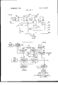
Consideration will now be given grams of several of the system components of FIGS. 2 and 3. Referring to FIG. 6, there is illustrated a schematic circuit diagram of a simple MOSFET single-pole, single-throw switch 300, the single MOSFET switch being a basic device from which numerous MOSFET logic components of varying complexity can be fabricated. As shown, the device 300 includes a source electrode 301, a drain electrode 302 corresponding to the output, and a gate electrode 303 corresponding to the input. The source is connected to ground. For a P-channel MOSFET the drain electrode 302 is connected to a negative potential V through a load resistor 304. In response to a negative control signal applied to the gate electrode 303 of sufficient magnitude above its threshold voltage to cause satu ration, the device becomes highly conductive in accordance with a closed-switch condition. In the presence of a control signal applied to the gate electrode less than threshold, e.g., at ground, the device is essentially nonconductive in accordance with an open switch position. it is seen that for an open-switch condition with a ground control signal applied, the output is negative. For a negative control signal to close the switch, the output increases positively. Thus, an inversion is provided between input and output.
In FIG. 7 there is illustrated a seven-input rotary switch matrix such as may be included in the described rotary switch networks. The rotary switch matrix comprises seven MOSFET switching devices 310. input terminals 311 are connected to the respective drain electrodes of switches 310. Control ter minals 312 are connected by control lines G, through G, to the gate electrodes of switches 310. The source electrodes of switching devices 310 are connected jointly to an output terminal 313. In the operation binary bits of logic 1'5" and 0s applied to input terminals 311 are selectively switched to output terminal 313 by a sequential application of control signals to the control lines G, through 6,. For use in the networks 121, and 129, the input terminals 311 are supplied with inputs representing single bits of successively higher order to schematic circuit diadigits. For use in the matrix 132 the input terminals 311 and the output terminal 313 become interchanged, there being the load device 340, the source electrode of which is connected to the junction of the drain electrodes of devices 341, 342 and 343. The source electrodes of devices 341, 342 and 343 are each connected to ground. Input terminals 344, 345 and 346 are connected at the gate electrodes of each of said switching devices, an output terminal 347 being at the junction of the drain electrodes.
In a typical operation, a logic input, corresponding to a V volts, is applied to at least one of the input terminals 344, 345 and 346 for turning ON the associated MOSFET device, and will generate a I at the output terminal 347, corresponding to zero volts. Conversely, a logic l is applied to all of the input terminals so as to turn OFF all of said devices, and will generate a logic "0 at said output terminal.
It may be appreciated that a wide range of multi-input NAND gates may be readily constructed by supplying the appropriate number of parallel connected MOSFET switching devices. It may also be noted that by adding an inverter function to the output of a NAND gate, there is provided an AND gate operation. The inverter function is readily supplied by a single MOSFET switching device.
FIG. 9 provides a schematic circuit diagram of a single pregate component of pregate network 122. Comprised are three two-input NAND- gates 350, 351 and 352. There are four input terminals 353, 354, 356 and 357 and two output terminals 358 and 359. Input terminals 353 and 354 are coupled to NAND-gate 350 and have respectively applied thereto an add control signal and a single true binary bit, shown as X,. lnput terminals 356 and 357 are coupled to NAND-gate 351 and have respectively applied thereto the complement of the binary bit applied to terminal 354, viz, X and a subtract control signal. The outputs of gates 350 and 351 are applied as inputs to NAND-gate 352. A first direct output from NAND- gate 352 is taken at output 358 and a second inverted output is taken at terminal 359. The output terminals 358 and 359 are applied to a full adder-subtracter component of the network 240 as described with respect to FIG. 10.
For an add operation, a logic 1 is applied to the add terminal 354 and a logic 0" to the subtract terminal 356. The inverse is true for subtraction. Considering an exemplary add operation where the true input signal is a logic I terminals 353 and 354 both have logic "1s applied and generate a logic 0" at the output of NAND-gate 350. Terminals 356 and 357 both have logic 0s" applied, generating a logic I at the output of NAND-gate 351. A logic I will appear at terminal 358 and a logic 0 at terminal 359. For a subtract operation of a logic l the outputs will be inverted.
' With reference to FIG. 10, there is illustrated a schematic circuit diagram of a full adder-subtracter component such as included in network 124. This component performs addition and subtraction on a given pair of bits of corresponding digits of two binary-coded decimal numbers, the component operating in digit sequence. Included are two input NAND- gates 370, 371, 37 2 and 373 for generating a single true output and two- input NANDgates 374, 375 and 376 for generating outputs of both their true and complementary value. There are four input terminals 377, 378, 379 and 380 having applied thereto true and complementary input signals, and two input terminals 381 and 382 having applied true and complementary carry and borrow signals. A pair of output terminals 383 and 384 provide true and complementary sum and difference outputs, and a further pair of output terminals 385 and 386 provide true and complementary carry and borrow signals. Input terminals 377 and 378 are coupled to NAND-gate 370,
and terminals 379 and 380 are coupled to NAND-gate 371. The outputs of NAND-gates 370 and 371 are coupled to NAND-gate 374, and an output of gate 370 is also coupled to NAND-gate 375. True and complementary outputs of NAND- gates 374 are coupled to NAND- gates 373 and 372, respectively. Input terminals 381 and 382 complete the input connection to NAND- gates 372 and 373, respectively. The output of NAND-gate 372 is connected to NAND- gates 375 and 376. The true and complementary outputs of gate 375 are connected to terminals 386 and 385, respectively, and true and complementary outputs of gate 376 are connected to terminals 383 and 384, respectively.
For an add operation, true values X, and Y, are connected to terminals 377 and 378, respectively, and their complements X, and Y, are connected to input terminals 379 and 380, respectively. True and complementary values of a carry signal are connected to input terminals 381 and 382, respectively. The true sum S, is obtained at output terminal 384 and its complement S, is obtained at terminal 383. A true carry C, appears at terminal 386 and its complement C, at 385. For a subtract operation, true values X, and Y, are connected to input terminals 379 and 378, respectively, and their complements X, and Y, are connected to terminals 377 and 380, respectively. True and complementary borrow signals B, and E, are connected to terminals 381 and 382, respectively. The true difference signal D, appea rs at output tenninal 383 and the complement of this value D, is obtained at terminal 384. A true borrow B, appears at terminal 386 and its complement E, at terminal 385.
To briefly illustrate one exemplary operation of the component of FIG. 10, an addition of two binary bits each having a logic value I with an applied carry of 1" will be considered. Accordingly, X, and Y, are each I," X, and Y, are each 0"; and C, and C, are l and 0," respectively. NAND-gate 370 will generate a logic 0" and NAND-gate 371 a logic I. The true output at NAND-gate 374 will be a 1" and its complementary output a NAND- gates 372 and 373 will in turn each generate a logic I." With a logic "1 applied to each input of NAND-gate 376, output terminal 384 will generate a 0. With a logic 1" and 0" applied to NAND-gate 375, output terminal 386 will generate a 1.
A schematic circuit diagram of an error-sensor network 126 of FIGS. 2 and 3 is shown in FIG. 11. Component 126 includes two input NAND- gates 390, 391, 392, 393 and 394 and three input NAND-gate 395. Also provided are input terminals 396, 397, 398, 399 400, 401 and 402 and a single-output terminal 403. Input terminals 396 and 397 are connected to a NAND- gate 390, and terminals 397 and 398 are connected to gate 391. The outputs of gates 390 and 391 and input terminal 399 are connected to gate 395. The output of gate 395 and input terminal 400 are connected to gate 392. Input tenninals 401 and 402 are connected to gate 393. The outputs of gates 392 and 393 are connected to gate 394 from which output terminal 403 is fed. This component has the true sum outputs 8,, S and S, from full adder- subtracter components 243 and 242, respectively, of FIG. 3 as well as the complementary carry output C, from component 243 coupled to input terminals 396, 397, 398 and 399, respectively. Add and subtract control signals and the true borrow signal 13,, from component 243 are connected to input terminals 400, 401 and 402, respectively. For a condition in which an uncorrected sum or difi'erence is generated by full adder-subtracter network 124 of FIGS. 2 and 3 a signal is generated at output terminal 403 which is employed to activate the MPDT switch 123 of FIGS. 2 and 3. For example, with a logic l at input terminals 399 and 400, indicative of carry for an add operation; or with a logic I at terminals 401 and 402, indicative of borrow for a subtract operation, or with a logic "I at terminal 397 and at either of terminals 396 and 398 for either an add or subtract operation, there will be generated a 1" at output terminal 403.
In FIG. 12 is a schematic circuit diagram of the binarycoded decimal rate multiplier 131 of FIGS. 2 and 3. The multiplier comprises a four-stage binary counter including conventional 1K flip- flop stages 410, 411, 412 and 413. Each flip flop stage has a J, K and CP input and a Q and {5 output. Also included are four two-input NANl)gates 414, 4K5, 4th and 417 and a four-input HAND-gate 418. One input terminal Milli has a clock signal applied which is connected to the Cl inputs of each counter stage. Further input terminals 421, Mill, Md and 24 are connected, respectively, as inputs to NAND- gatcs 417, 416, 415 and 414. Second inputs are applied to NAHU- gates 414 through 417 from the 6 outputs of stages 410 through 413, respectively. As the multiplier is connected in FIG. 3, binary bits a1, a2, a4 and 118 of a given digit are ap plied from successive stages of storage registers 114d through 247, respectively, to input terminals 421, 4122, 43 and 42.4. An output terminal 425 is taken from HAND-gate 4118, providing a unary pulse code which corresponds to the binary'coded decimal digit applied to input terminals ill through fl t. A logic 1, ground, is applied to inputs 1 and it or stage did. The Q output of stage 410 is connected to .l and K inputs of stage 411 and is further connected to AND-gate 42b. The output of stage 411 is also connected to ANl'JLgate 412.6. The output of gate 426 is connected to inputs 3 and K. of stage 412 and to an input of AND-gate 427, and provides an output connected to inputs .l and K. of stage 413. RC differentiating pairs 428 connects the U outputs of each of the flip-flop stages to their respective HAND gates for distinguishing in time the pulses applied to said NAND gates. The outputs of NANlIl-gates 414 through 417 are connected as inputs to HAND-gate did. The output of gate 417 is also connected to an output terminal 429 for supplying trigger pulses to the down counter 13d.
Considering the operation of the binary-coded rate decimal multiplier 131 of MG. 12, there are 16 cloclr pulses applied each counting period Ar. in response to a clock input signal frequency f,,, signals are provided from the U terminal outputs of stages 410, 411, 412 and 413 at diminishing frequencies of f /2 f,. l8 and f /l6 respectively. As a function of the binary hit signals applied to input terminals 421 through 424, one or more of the HAND-gates 414 through 417 will generate a 0" which in turn causes a l to be generated at the output terminal 425 for each time one of the previous HAND gates generates a 0. This l" is no longer a binary pulse but is now in the form of a unary pulse. For example, consider the decimal digit six to be applied to the rate multiplier which in binary-coded decimal torm provides a l energization at input terminals 422 and 423, NAND-gate Hill will generate a 0" at a frequency off /4 which will amount to four pulses for every 16 clock pulses, and HAND-gate 416 will generate a 0 frequency f,.f8 amounting to two pulses for every 16 clock pulses. Thus, six pulses appear at the output terminal 425 per Ar. Correspondingly, an applied digit three will generate three pulses per A: at terminal 425, etc.
In FIG. 13 there is illustrated a functional block diagram for performing a division operation, employing the multiplication and addition-subtraction circuitry with respect to Phil. El. For an operation of Q Z/R, the reciprocal Tof the divisor R is obtained through an iterative process and then multiplied by the dividend so that =21. An iterative formula for computing the reciprocal of the quantity T==1IR is:
n-1= i( i)U= 2 lim T'"-llR 1:? it may be determined that for a most significant digit of ii! of or greater, selecting the initial value of T, equal to 4/3, obtains a sufficiently close approximation of T to till after four alteralions.
Considering MG. 13, there is illustrated a first storage net work 500' into which the dividend Z is entered and a second storage network Sill into which the divisor R is entered. The storage networks 500 and 501 may be similar to networks 12.0 and 128 of FIG. 2. The output of storage network 501 is coupled to a comparator network 502 and also to a multiplier circuit 503. The output of storage 500 is also coupled to circuit 503 as is a source 504 for storing the BCD number two. The multiplier circuit 503 includes components illustrated in FIG.
3 for providing a multiplication of each of the applied inputs by the number two. A source 505 for storing the BCD number five is coupled as the second input to comparator network 502 t'or making a comparison with the most significant digit of the divisor R. For most significant digits less than five a signal is applied to the multiplier circuit 503 for causing it to multiply both the divisor R and the dividend Z by two, which products are fed back to the storage networks 500 and 501. A second comparison is then made in the comparator network 502 and if the most significant digit is still less than five the multiplication process is repeated. When the most significant digit exceeds 5 the modified divisor R is coupled as a first input to a multiplier circuit 506.
A source 507 for storing a decimal constant of 4/3 the ini tial value oi l", is coupled to storage network 508 and the output applied as a second input to the multiplier circuit 506. The multiplier circuit 506 multiplies this constant by R the resulting product being coupled to a subtract circuit 509 as the subtrahend. Also coupled to the subtract circuit 509 as the minuend is the constant from source 504. The difference at the output of circuit 509 is (2-R'T,). This quantity is applied to a further multiplier circuit 510. Also connected to multiplier circuit 510 through a delay circuit 511 is the quantity from network 508. The product output of multiplier circuit 510, the quantity T, (2 1? T is connected to the storage network 508 and becomes the new value T, +1 which is now coupled to multiplier circuit 506 and, with delay, to multiplier circuit fillll. The process is repeated for three traversals of the closed loop at the end of which time the output from storage network 508 is coupled through gate 512 and is applied to a final multiplicr circuit 513 to which is also applied modified dividend Z. The output quotient Z/R appears at the output of multiplier circuit 513.
What I claim as new and desire to secure by Letters Patent of the United States is:
1. An electronic calculator for performing multiplication operations of two multidigit binary-coded decimal numbers, comprising:
a. a first storage network for storing one of said numbers,
said first storage network including four multistage registers, one register for each binary bit order of the stored decimal digits,
b. a second storage network for storing the other of said numbers, said second storage network including four multistage registers, one register for each binary bit order of of the stored decimal digits,
c. A tour-stage binary-coded decimal counter,
a first switch network for applying in parallel the binary bits of each digit of said one number to the stages of said binary-coded decimal counter,
e. a binary-coded decimal rate multiplier for generating dur ing a given period unary pulses proportional in number to an applied input quantity,
i. a second switch network for applying in parallel the binary bits of each digit of said other number to said rate multiplier for determining the number of unary pulses generated during each given period,
g. an accumulator network comprising multiple binarycoded decimal counter stages, one for each bit order of the processed decimal digits,
h. a third switch network for applying the generated unary pulses from said rate multiplier in an advancing succession to the counter stages of said accumulator network,
i. means for applying a trigger signal to said binary'coded decimal counter once each given period for causing said binary-coded decimal counter to count one unit, and
j. detection means responsive to the count in said decimal counter for terminating the generation of said unary pulses from said rate multiplier upon said count reaching a given reference value, whereby the generated unary pulses are a function of the product of digits applied to said decimal counter and to said rate multiplier.
2. An electronic calculator as in claim 1 wherein said first switch network is operated in a first digital sequence and said second switch network is operated in a second digital sequence having a multiple relationship with said first digital sequence so as to provide a cross products of the digits of said two binary-coded decimal numbers.
3, An electronic calculator as in claim 2 wherein said binary-coded decimal counter is operated in a countdown mode and said detection means comprises a zero detector responsive to a zero count of said decimal counter for terminating the generation of said unary pulses.
4. An electronic calculator as in claim 3 which employs integrated circuit MOSFET devices in its construction.
5. An electronic calculator for performing division operations of two decimal numbers, comprising:
first storage means for storing the dividend and divisor,
b. comparator means for comparing the most significant digit of the divisor stored in said first storage means with a first constant and generating a first output when said constant is the larger value, a second output when said constant is the lesser value or an equal value,
c. first multiplier means responsive to said first output of said comparator means for multiplying said dividend and divisor by a second constant to provide a modified dividend and divisor,
. means for coupling said modified dividend and divisor back to said first storage means,
. second storage means for storing a given value and having a third constant initially stored therein,
. second multiplier means responsive to said second comparator for multiplying said modified divisor by the value stored in said second storage means,
subtracter means for subtracting the output of said second multiplying means from said second constant,
. third multiplier means for multiplying the output of said fourth multiplier means for multiplying the updated value stored in said second storage means by said modified dividend for obtaining the quotient of said two decimal numbers.
Claims (5)
1. An electronic calculator for performing multiplication operations of two multidigit binary-coded decimal numbers, comprising: a. a first storage network for storing one of said numbers, said first storage network including four multistage registers, one register for each binary bit order of the stored decimal digits, b. a second storage network for storing the other of said numbers, said second storage network including four multistage registers, one register for each binary bit order of of the stored decimal digits, c. A four-stage binary-coded decimal counter, d. a first switch network for applying in parallel the binary bits of each digit of said one number to the stages of said binary-coded decimal counter, e. a binary-coded decimal rate multiplier for generating during a given period unary pulses proportional in number to an applied input quantity, f. a second switch network for applying in parallel the binary bits of each digit of said other number to said rate multiplier for determining the number of unary pulses generated during each given period, g. an accumulator network comprising multiple binary-coded decimal counter stages, one for each bit order of the processed decimal digits, h. a third switch network for applying the generated unary pulses from said rate multiplier in an advancing succession to the counter stages of said accumulator network, i. means for applying a trigger signal to said binary-coded decimal counter once each given period for causing said binarycoded decimal counter to count one unit, and j. detection means responsive to the count in said decimal counter for terminating the generation of said unary pulses from said rate multiplier upon said count reaching a given reference value, whereby the generated unary pulses are a function of the product of digits applied to said decimal counter and to said rate multiplier.
2. An electronic calculator as in claim 1 wherein said first switch network is operated in a first digital sequence and said second switch network is operated in a second digital sequence having a multiple relationship with said first digital sequence so as to provide a cross products of The digits of said two binary-coded decimal numbers.
3. An electronic calculator as in claim 2 wherein said binary-coded decimal counter is operated in a countdown mode and said detection means comprises a zero detector responsive to a zero count of said decimal counter for terminating the generation of said unary pulses.
4. An electronic calculator as in claim 3 which employs integrated circuit MOSFET devices in its construction.
5. An electronic calculator for performing division operations of two decimal numbers, comprising: first storage means for storing the dividend and divisor, b. comparator means for comparing the most significant digit of the divisor stored in said first storage means with a first constant and generating a first output when said constant is the larger value, a second output when said constant is the lesser value or an equal value, c. first multiplier means responsive to said first output of said comparator means for multiplying said dividend and divisor by a second constant to provide a modified dividend and divisor, d. means for coupling said modified dividend and divisor back to said first storage means, e. second storage means for storing a given value and having a third constant initially stored therein, f. second multiplier means responsive to said second comparator for multiplying said modified divisor by the value stored in said second storage means, g. subtracter means for subtracting the output of said second multiplying means from said second constant, h. third multiplier means for multiplying the output of said subtracter means by the value stored in said second storage means, the output of said third multiplier means being coupled to said second storage means for updating the stored value, after several updatings said stored value closely approximating the reciprocal quantity of the modified divisor, and i. fourth multiplier means for multiplying the updated value stored in said second storage means by said modified dividend for obtaining the quotient of said two decimal numbers.
Applications Claiming Priority (1)
| Application Number | Priority Date | Filing Date | Title |
|---|---|---|---|
| US81696569A | 1969-04-17 | 1969-04-17 |
Publications (1)
| Publication Number | Publication Date |
|---|---|
| US3614404A true US3614404A (en) | 1971-10-19 |
Family
ID=25222039
Family Applications (1)
| Application Number | Title | Priority Date | Filing Date |
|---|---|---|---|
| US816965A Expired - Lifetime US3614404A (en) | 1969-04-17 | 1969-04-17 | Electronic calculator |
Country Status (1)
| Country | Link |
|---|---|
| US (1) | US3614404A (en) |
Cited By (2)
| Publication number | Priority date | Publication date | Assignee | Title |
|---|---|---|---|---|
| US3720820A (en) * | 1971-03-18 | 1973-03-13 | Tektranex Inc | Calculator with a hierarchy control system |
| US3975835A (en) * | 1975-02-19 | 1976-08-24 | The Singer Company | Computer applications trainer |
Citations (7)
| Publication number | Priority date | Publication date | Assignee | Title |
|---|---|---|---|---|
| US2928601A (en) * | 1952-03-25 | 1960-03-15 | Hughes Aircraft Co | Arithmetic units for decimal coded binary computers |
| US3112396A (en) * | 1957-05-03 | 1963-11-26 | Ibm | Arithmetic circuitry |
| US3278734A (en) * | 1961-09-05 | 1966-10-11 | Telefunken Patent | Coded decimal adder |
| US3304418A (en) * | 1964-03-02 | 1967-02-14 | Olivetti & Co Spa | Binary-coded decimal adder with radix correction |
| US3460129A (en) * | 1964-03-09 | 1969-08-05 | Ericsson Telefon Ab L M | Frequency divider |
| US3508037A (en) * | 1967-01-30 | 1970-04-21 | Sperry Rand Corp | Decimal add/subtract circuitry |
| US3513303A (en) * | 1964-03-21 | 1970-05-19 | Bell Punch Co Ltd | Desk calculator for performing addition,subtraction,multiplication and division |
-
1969
- 1969-04-17 US US816965A patent/US3614404A/en not_active Expired - Lifetime
Patent Citations (7)
| Publication number | Priority date | Publication date | Assignee | Title |
|---|---|---|---|---|
| US2928601A (en) * | 1952-03-25 | 1960-03-15 | Hughes Aircraft Co | Arithmetic units for decimal coded binary computers |
| US3112396A (en) * | 1957-05-03 | 1963-11-26 | Ibm | Arithmetic circuitry |
| US3278734A (en) * | 1961-09-05 | 1966-10-11 | Telefunken Patent | Coded decimal adder |
| US3304418A (en) * | 1964-03-02 | 1967-02-14 | Olivetti & Co Spa | Binary-coded decimal adder with radix correction |
| US3460129A (en) * | 1964-03-09 | 1969-08-05 | Ericsson Telefon Ab L M | Frequency divider |
| US3513303A (en) * | 1964-03-21 | 1970-05-19 | Bell Punch Co Ltd | Desk calculator for performing addition,subtraction,multiplication and division |
| US3508037A (en) * | 1967-01-30 | 1970-04-21 | Sperry Rand Corp | Decimal add/subtract circuitry |
Cited By (2)
| Publication number | Priority date | Publication date | Assignee | Title |
|---|---|---|---|---|
| US3720820A (en) * | 1971-03-18 | 1973-03-13 | Tektranex Inc | Calculator with a hierarchy control system |
| US3975835A (en) * | 1975-02-19 | 1976-08-24 | The Singer Company | Computer applications trainer |
Similar Documents
| Publication | Publication Date | Title |
|---|---|---|
| US3777132A (en) | Method and apparatus for obtaining the reciprocal of a number and the quotient of two numbers | |
| GB815751A (en) | Improvements in electric calculators and accumulators therefor | |
| US3535498A (en) | Matrix of binary add-subtract arithmetic units with bypass control | |
| US3614404A (en) | Electronic calculator | |
| GB1098853A (en) | Computing machine | |
| US3456098A (en) | Serial binary multiplier arrangement | |
| US3036770A (en) | Error detecting system for a digital computer | |
| US3426184A (en) | Logarithmic circuit | |
| US3462589A (en) | Parallel digital arithmetic unit utilizing a signed-digit format | |
| GB869703A (en) | Electronic computer | |
| GB1189148A (en) | Computer | |
| US3155822A (en) | Recirculating adder | |
| Bashagha et al. | Radix digit-serial pipelined divider/square-root architecture | |
| US2928600A (en) | Binary to decimal radix conversion apparatus | |
| US3622768A (en) | Dual key depression for decimal position selection | |
| GB976620A (en) | Improvements in or relating to multiplying arrangements for digital computing and like purposes | |
| SU675422A1 (en) | Multiplier | |
| SU734682A1 (en) | Divider | |
| GB852182A (en) | Cyclically operable electrical calculating apparatus | |
| SU742929A1 (en) | Device for extraction of n-th root | |
| SU598075A1 (en) | Divider | |
| SU682894A1 (en) | Arithmetical apparatus | |
| EP0450751B1 (en) | High speed digital divider | |
| SU448461A1 (en) | Device for dividing numbers | |
| Negi et al. | Implementation of high speed radix-10 parallel multiplier using Verilog |