US3603832A - Image intensifier with channel-type secondary emission multiplier - Google Patents
Image intensifier with channel-type secondary emission multiplier Download PDFInfo
- Publication number
- US3603832A US3603832A US785846A US3603832DA US3603832A US 3603832 A US3603832 A US 3603832A US 785846 A US785846 A US 785846A US 3603832D A US3603832D A US 3603832DA US 3603832 A US3603832 A US 3603832A
- Authority
- US
- United States
- Prior art keywords
- screen
- channel
- photocathode
- membrane
- multiplier
- Prior art date
- Legal status (The legal status is an assumption and is not a legal conclusion. Google has not performed a legal analysis and makes no representation as to the accuracy of the status listed.)
- Expired - Lifetime
Links
- 239000012528 membrane Substances 0.000 claims abstract description 32
- 229910052782 aluminium Inorganic materials 0.000 claims description 12
- XAGFODPZIPBFFR-UHFFFAOYSA-N aluminium Chemical group [Al] XAGFODPZIPBFFR-UHFFFAOYSA-N 0.000 claims description 12
- 229910052751 metal Inorganic materials 0.000 claims description 9
- 239000002184 metal Substances 0.000 claims description 9
- 239000000463 material Substances 0.000 claims description 2
- 239000011810 insulating material Substances 0.000 claims 1
- 239000011159 matrix material Substances 0.000 description 15
- 230000000694 effects Effects 0.000 description 4
- 239000011521 glass Substances 0.000 description 4
- 230000005855 radiation Effects 0.000 description 4
- OAICVXFJPJFONN-UHFFFAOYSA-N Phosphorus Chemical compound [P] OAICVXFJPJFONN-UHFFFAOYSA-N 0.000 description 3
- 150000002500 ions Chemical class 0.000 description 3
- 239000004922 lacquer Substances 0.000 description 3
- 238000000034 method Methods 0.000 description 3
- 230000003287 optical effect Effects 0.000 description 3
- 230000009467 reduction Effects 0.000 description 3
- 239000003795 chemical substances by application Substances 0.000 description 2
- 238000003384 imaging method Methods 0.000 description 2
- 238000004519 manufacturing process Methods 0.000 description 2
- 239000000758 substrate Substances 0.000 description 2
- QVGXLLKOCUKJST-UHFFFAOYSA-N atomic oxygen Chemical compound [O] QVGXLLKOCUKJST-UHFFFAOYSA-N 0.000 description 1
- 230000015572 biosynthetic process Effects 0.000 description 1
- 239000013590 bulk material Substances 0.000 description 1
- 230000015556 catabolic process Effects 0.000 description 1
- 230000008859 change Effects 0.000 description 1
- 150000001875 compounds Chemical class 0.000 description 1
- 238000010276 construction Methods 0.000 description 1
- 230000001186 cumulative effect Effects 0.000 description 1
- 238000009826 distribution Methods 0.000 description 1
- 230000005684 electric field Effects 0.000 description 1
- 238000005188 flotation Methods 0.000 description 1
- 230000006872 improvement Effects 0.000 description 1
- 230000004048 modification Effects 0.000 description 1
- 238000012986 modification Methods 0.000 description 1
- 229910052760 oxygen Inorganic materials 0.000 description 1
- 239000001301 oxygen Substances 0.000 description 1
- 238000009304 pastoral farming Methods 0.000 description 1
- 230000008569 process Effects 0.000 description 1
- 230000007480 spreading Effects 0.000 description 1
- 238000003892 spreading Methods 0.000 description 1
- XLYOFNOQVPJJNP-UHFFFAOYSA-N water Substances O XLYOFNOQVPJJNP-UHFFFAOYSA-N 0.000 description 1
Images

Classifications
-
- H—ELECTRICITY
- H01—ELECTRIC ELEMENTS
- H01J—ELECTRIC DISCHARGE TUBES OR DISCHARGE LAMPS
- H01J43/00—Secondary-emission tubes; Electron-multiplier tubes
- H01J43/04—Electron multipliers
- H01J43/06—Electrode arrangements
- H01J43/18—Electrode arrangements using essentially more than one dynode
- H01J43/24—Dynodes having potential gradient along their surfaces
-
- H—ELECTRICITY
- H01—ELECTRIC ELEMENTS
- H01J—ELECTRIC DISCHARGE TUBES OR DISCHARGE LAMPS
- H01J31/00—Cathode ray tubes; Electron beam tubes
- H01J31/08—Cathode ray tubes; Electron beam tubes having a screen on or from which an image or pattern is formed, picked up, converted, or stored
- H01J31/50—Image-conversion or image-amplification tubes, i.e. having optical, X-ray, or analogous input, and optical output
- H01J31/506—Image-conversion or image-amplification tubes, i.e. having optical, X-ray, or analogous input, and optical output tubes using secondary emission effect
- H01J31/507—Image-conversion or image-amplification tubes, i.e. having optical, X-ray, or analogous input, and optical output tubes using secondary emission effect using a large number of channels, e.g. microchannel plates
Definitions
- Trifari ABSTRACT An electronic image intensifier including an electron multiplier.
- the device comprises a photocathode, a fluorescent screen, and a body between and spaced from the photocathode and screen.
- the body is provided with a plurality of elongated, longitudinal passageways, the walls of which are secondary emissive. Electrodes are provided on opposite surfaces bounding the channels and an electrically conductive electron permeable membrane covering the entrance to each passageway.
- PATENTEUSEP 71911 31503332 SHEET 1 BF 2 INVENTORS BRIAN W MANLEY BY PIETER SCHAGEN JOHN ADA s 2M 1e AG T PATENTED SEP 7
- This invention relates to electron multiplier and image intensifier devices. More particularly the invention relates to channel intensifier devices and to electronic tubes employing such devices. Such. devices will be defined later but, briefly, they are secondary-emissive electron-multiplier devices comprising a matrix in the form of a plate having a large number of elongated channels passing through its thickness, said plate having a first conductive layer on its input 1 face and a separate second conductive layer on its output face to act respectively as input and output electrodes.
- a potential difference is applied between the two electrode layers of the matrix so as to set up an electric field to accelerate the electrons, which field establishes a potential gradient created by current flowing through resistive surfaces formed inside the channels or (if such resistive surfaces are absent) through the bulk material of the matrix.
- Secondary-emissive multiplication takes place in the channels and the output electrons may be acted upon by a further accelerating field which may be set up between the output electrode and a suitable target, for example a luminescent display screen.
- channel intensifier devices are devices having a structure as defined in the Patent Specifications referred to above in a definition given in the following terms:
- a channel intensifier device is a secondary-emissive electron multiplier device for an electronic tube which device comprises a resistive matrix in the form of a plate the major surfaces of which constitute the input and output faces of the matrix, a conductive layer on the input face of the matrix serving as an input electrode, a separate conductive layer on the output face of the matrix serving as an output electrode, and elongated channels each providing a passageway from one face of the assembly consisting of matrix and input and output electrodes to the other face of said assembly.
- the distribution and cross sections of the channels :and the resistivity of the matrix are such that the resolution and electron multiplication characteristic of any one'unit area of the device is sufficiently similar to that of any other unit area for any imaging purposes envisaged.
- an imaging tube or system If such a device is used in an imaging tube or system, the latter will be referred to for convenience as an image intesifier tube or system rather than as an image converter tube or system even in applications where the primary purpose is a change in the wavelength of the radiation of the image.
- One of the problems with present channel intensifier devices when used in a tube with a display screen is feedback of positive ions created inside the channels or at the display screen. These ions can be accelerated by the field in the channels and can thus cause secondary electron emission at the photocathode.
- the problem in question is the occurrence of electrical breakdown between channel plate and screen due to the high field which has to be set up between them in order to enable electrons to penetrate the metal backing of the screen and maintain good resolution.
- lt is an object of the present invention to permit both of these problems to be solved by means of an improved channel plate construction. It is a further object of the invention to provide a solution to the "dark spot" problem as will be explained.
- An improvement in or modification of a channel intensifier device as herein defined including an electrically conductive membrane obturating the entrance to each channel which membrane is electron-permeable as defined and is electrically connected to the other membranes.
- electron-permeable is used in the sense that individual electrons can penetrate through a membrane or can produce secondary electrons within the membrane which emerge from the output side thereof.
- the membranes may be formed as a continuous layer which is superimposed on the input electrode. in such case the membrane layer may be insulated from the input electrode so as to permit it to be held at a potential different from that of said electrode.
- the membranes may be formed as extensions of the input electrode of the device so that said electrode and membranes form, together, a continuous layer.
- the membranes are substantially opaque to visible radiation (and possibly other radiation such as ultraviolet) since this permits the device to perform also the second function of preventing or reducing optical feedback when used in a tube with a display screen.
- substantially opaque is used to indicate that the membranes must be at least sufficiently opaque to backward radiation from the display screen to prevent cumulative or runaway optical feedback in the tube).
- the screen requires no metal backing and the material of the screen is chosen to emit light of wavelengths to which the members are substantially opaque.
- an image intensifier tube including the channel intensifier device in operative combination with a display screen on the output side thereof which screen is adapted to emit light of wavelengths to which the membranes are substantially opaque, a photocathode spaced from the input side of said device, and an electron-optical system between said photocathode and said device which system is of the type designed to effect an electron-optical inversion of the image.
- a typical example of such an electronoptical system is the so-called electron-optical diode system or equivalents thereof employing more than two electrodes, and the tube may follow a preceding fiber-optically coupled electron-optical image-inverting tube so that the combined system produce an output image which has the same orientation as the input image).
- FIG. 1 is a prior art device shown diagrammatically.
- FIG. 2 is a diagrammatic view of one embodiment of the invention.
- FIGS. 3, 4 and 5 are diagrammatic views of other embodiments of the invention.
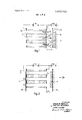
- FIG. 1 of the accompanying drawing shows a small part of a known channel intensi' bomb device (with its channels C, input electrode E1, and output electrode E2) and a part of a cooperating display screen S.
- the screen may be of conventional type laid on a plain glass or fiber-optic window W which may form part of an evacuated envelope.
- the screen comprises a layer of phosphor S and a metal backing E3 (typically aluminum) which is electronpermeable but substantially opaque to light emitted rearwardly by the phosphor.
- distance d What would really be desirable is to reduce distance d to a very small value and then reduce voltage V even more, for example making distance d equal to 0.5 mm. and making the voltage V equal to 1.25 kv., which is only 2.5 kv./mm. However, a minimum of 5 kv. is needed to penetrate the aluminum screen backing E3 which is provided to prevent light feedback. Therefore distance d must be at least 1 mm. which means that there is still a limiting field strength and only just enough resolution.
- the metal film is effectively constituted by membranes or diaphragms D which are shown obturating the entrances to the channels C.
- membranes are conductive (e.g. aluminum) and may be formed as a continuous layer of film Df which is superimposed on the input electrode E1 of the channel intensifier device as shown.
- Such membrane layer Df may be in contact with El as shown or it may be insulated from the input electrode E1 so as to permit it to be held at a potential different from that of said electrode (see insulating layer Id in FIG. 3.)
- the membranes D may be formed as extensions of the input electrode E1 of the device so that said electrode and membranes form, together, a continuous layer as shown in FIG. 4.
- an arrangement of a channel plate I with a screen 5 in accordance with FIG. 2, FIG. 3 or FIG. 4 can be preceded by an electron-optical diode image-inverting stage as indicated in FIG. 5, such stage having, say, several centimeters of axial depth so that a high voltage of, say 5 kv. can be applied (by a source Bo) without risk between its photocathode P and its conical anode A.
- the latter can, if desired, have a potential different from that of electrode E1, or anode A may be connected to electrode El as shown so that the first stage becomes a simple electron-optical diode.
- the electrons from the photocathode penetrate easily through membranes D and the latter stop light feedback and also allow the voltage between the channel plate and screen to be reduced with an accompanying reduction of the spacing between channel plate and screen.
- the screen is still just as bright as, or brighter than, aluminized screen at 5 kv.
- the E2-S spacing a' (FIG. 2) can be made 0.5 mm. and the voltage from B2 can be 1.5 kv. (i.e. 3 kv./mm.).
- Such a field strength allows the resolution to be slightly better than with 5 v. at l mm. and there is virtually no danger of field emission (which was made worse in any case by the presence of the aluminum film in the arrangement of FIG. 1).
- the membranes can stop ion feedback, a function which, of course, could not be performed by the conventional metal backing E3 of FIG. 1.
- the invention has particular advantages in relation to tubes in which the channel plate is remote from the photocathode (e.g. the tube of FIG. 5), it can also be applied usefully to some tubes of the proximity" type, i.e. tubes in which the photocathode is placed near to the channel intensifier device without intermediate electron-optical focusing means. This can arise in cases where the resolution required is sufficiently low to allow the channel plate to be spaced from the photocathode by a distance of a few millimeters thus allowing voltages of several kvs. to be applied between them.
- a practical example of this is an X-ray image intensifier in which this spacing is 5 mm. and the applied voltage is 4 kv.
- the membranes D can be made as separate elements with their edges in electrical contact with the input electrode, but the use of a continuous layer or film Df permits easier manufacture, which can be carried out as follows.
- a lacquer film is formed by methods well known in the art e.g. flotation water.
- SAid film is then placed over the input face of a matrix which already has a separate input electrode as in FIGS. 2 or 3.
- aluminum is evaporated on to the film.
- the channel plate is baked (in known manner) so as to burn off the lacquer and leave an aluminum film in contact with the electrode E1 (FIG. 2) or a prepared insulating layer formed in El (as layer 1d of FIG. 3).
- the film is formed on a substrate (e.g. glass) from which it can be later released in known manner.
- Aluminum is then evaporated on to the film.
- the film is then released from the substrate and placed on the channel plate matrix with the aluminum side in contact with the matrix.
- the matrix is then baked to burn off the lacquer.
- the matrix is of glass and the necessary low degree of conductivity has been, or is to be, obtained by reduction of a metal (e.g. lead) compound in the glass
- the above process requires special measures since the baking is done in air or oxygen.
- the reduction can be repeated a second time after the baking, or it can be postponed until after the baking.
- a channel plate according to FIG. 2 may have substantially the following dimensions and values:
- Electrodes EI-E2 Niehrome evaporated at a grazing angle.
- An electronic image intensifier device including a photocathode, a fluorescent screen and a secondary emission multiplier between and spaced from the photocathode and 2.
- a device as claimed in claim I in which the screen is adapted to emit light of wavelengths to which the membrane is substantially opaque.
Landscapes
- Image-Pickup Tubes, Image-Amplification Tubes, And Storage Tubes (AREA)
Abstract
An electronic image intensifier including an electron multiplier. The device comprises a photocathode, a fluorescent screen, and a body between and spaced from the photocathode and screen. The body is provided with a plurality of elongated, longitudinal passageways, the walls of which are secondary emissive. Electrodes are provided on opposite surfaces bounding the channels and an electrically conductive electron-permeable membrane covering the entrance to each passageway.
Description
United States Patent Inventors Brian William Manley Burgess Hill; Pieter Schagen, Redhill; John Adams, East Grinstead, all of, England App], No 785,846
Filed Nov. 22, 1968 Patented Sept. 7, I971 Assignee U.S. Phillips Corporation New York, N.Y.
Priority Nov. 28, 1967 Great Britain 54133/67 IMAGE INTENSIFIER WITH CHANNEL-TYPE SECONDARY EMISSION MULTIPLIER 5 Claims, 5 Drawing Figs.
[15. Cl 313/95, 313/105, 250/213 VT Int. Cl ..H01j 31/50, HOlj 39/02,H0lj 39/14 Field of Search 313/74, 103-105, 95
[56] References Cited UNITED STATES PATENTS 1,907,507 5/1933 Coolidge 313/74 2,449,872 9/1948 Brasch et al. 313/74 2,584,814 2/1952 Rosenberg et a1.... 313/74X 3,449,582 6/1969 Sackinger 313/105 X 2,928,969 3/1960 Schneeberger... 313/95 X 3,062,962 11/1962 McGee 313/95 X Primary Examiner- Robert Segal Attorney-J rank R. Trifari ABSTRACT: An electronic image intensifier including an electron multiplier. The device comprises a photocathode, a fluorescent screen, and a body between and spaced from the photocathode and screen. The body is provided with a plurality of elongated, longitudinal passageways, the walls of which are secondary emissive. Electrodes are provided on opposite surfaces bounding the channels and an electrically conductive electron permeable membrane covering the entrance to each passageway.
PATENTEUSEP 71911 31503332 SHEET 1 BF 2 INVENTORS BRIAN W MANLEY BY PIETER SCHAGEN JOHN ADA s 2M 1e AG T PATENTED SEP 7 |97| 350K832 sum 2 or 2 LINVENTORS 2, W2
CH 0 BYJOHN ADAMS W L AGENT Ill IMAGE llNTENSIFlER WITH CHANNEL-TYPE SECONDARY EMHSSION MULTlllllLlllER This invention relates to electron multiplier and image intensifier devices. More particularly the invention relates to channel intensifier devices and to electronic tubes employing such devices. Such. devices will be defined later but, briefly, they are secondary-emissive electron-multiplier devices comprising a matrix in the form of a plate having a large number of elongated channels passing through its thickness, said plate having a first conductive layer on its input 1 face and a separate second conductive layer on its output face to act respectively as input and output electrodes.
Secondary-emissive intensifier devices of this character are described, for example, in British Pat. Specification Nos. 1,064,073 1,064,074 US. Pat. Nos. 3,387,137, 3,327,151 and 3,497,759, while methods of manufacture are described in British Pat. Specification Nos. 1,064,072 and 1,064,075.
In the operation of all these intensifier devices (when incorporated in electronic tubes) a potential difference is applied between the two electrode layers of the matrix so as to set up an electric field to accelerate the electrons, which field establishes a potential gradient created by current flowing through resistive surfaces formed inside the channels or (if such resistive surfaces are absent) through the bulk material of the matrix. Secondary-emissive multiplication takes place in the channels and the output electrons may be acted upon by a further accelerating field which may be set up between the output electrode and a suitable target, for example a luminescent display screen.
As a summary of this art, the devices referred to herein as channel intensifier" devices (or, more briefly, channel plates) are devices having a structure as defined in the Patent Specifications referred to above in a definition given in the following terms:
A channel intensifier device is a secondary-emissive electron multiplier device for an electronic tube which device comprises a resistive matrix in the form of a plate the major surfaces of which constitute the input and output faces of the matrix, a conductive layer on the input face of the matrix serving as an input electrode, a separate conductive layer on the output face of the matrix serving as an output electrode, and elongated channels each providing a passageway from one face of the assembly consisting of matrix and input and output electrodes to the other face of said assembly.
With such devices the distribution and cross sections of the channels :and the resistivity of the matrix are such that the resolution and electron multiplication characteristic of any one'unit area of the device is sufficiently similar to that of any other unit area for any imaging purposes envisaged.
If such a device is used in an imaging tube or system, the latter will be referred to for convenience as an image intesifier tube or system rather than as an image converter tube or system even in applications where the primary purpose is a change in the wavelength of the radiation of the image.
One of the problems with present channel intensifier devices when used in a tube with a display screen is feedback of positive ions created inside the channels or at the display screen. These ions can be accelerated by the field in the channels and can thus cause secondary electron emission at the photocathode.
A second problem arises owing to the need for a metal backing on the display screen which backing is usually provided to reflect light emitted rearwardly by the phosphor and .thus prevent or reduce optical feedback which would otherwise be caused by such light passing backwards through the channel plate and reaching the photocathode. The problem in question is the occurrence of electrical breakdown between channel plate and screen due to the high field which has to be set up between them in order to enable electrons to penetrate the metal backing of the screen and maintain good resolution.
lt is an object of the present invention to permit both of these problems to be solved by means of an improved channel plate construction. It is a further object of the invention to provide a solution to the "dark spot" problem as will be explained.
An improvement in or modification of a channel intensifier device as herein defined including an electrically conductive membrane obturating the entrance to each channel which membrane is electron-permeable as defined and is electrically connected to the other membranes.
The term electron-permeable" is used in the sense that individual electrons can penetrate through a membrane or can produce secondary electrons within the membrane which emerge from the output side thereof.
The membranes may be formed as a continuous layer which is superimposed on the input electrode. in such case the membrane layer may be insulated from the input electrode so as to permit it to be held at a potential different from that of said electrode.
Alternatively, the membranes may be formed as extensions of the input electrode of the device so that said electrode and membranes form, together, a continuous layer.
Preferably the membranes are substantially opaque to visible radiation (and possibly other radiation such as ultraviolet) since this permits the device to perform also the second function of preventing or reducing optical feedback when used in a tube with a display screen. (In this connection the term substantially opaque is used to indicate that the membranes must be at least sufficiently opaque to backward radiation from the display screen to prevent cumulative or runaway optical feedback in the tube). In such a tube the screen requires no metal backing and the material of the screen is chosen to emit light of wavelengths to which the members are substantially opaque.
For reasons connected mainly with the electron velocities required to penetrate the membranes, the following description will be based principally on a second aspect of the invention represented by the particular case of an image intensifier tube including the channel intensifier device in operative combination with a display screen on the output side thereof which screen is adapted to emit light of wavelengths to which the membranes are substantially opaque, a photocathode spaced from the input side of said device, and an electron-optical system between said photocathode and said device which system is of the type designed to effect an electron-optical inversion of the image. (A typical example of such an electronoptical system is the so-called electron-optical diode system or equivalents thereof employing more than two electrodes, and the tube may follow a preceding fiber-optically coupled electron-optical image-inverting tube so that the combined system produce an output image which has the same orientation as the input image).
The invention will be described with reference to the accompanying drawing in which:
FIG. 1 is a prior art device shown diagrammatically.
FIG. 2 is a diagrammatic view of one embodiment of the invention.
FIGS. 3, 4 and 5 are diagrammatic views of other embodiments of the invention.
The two problems already discussed will now be explained more fully with reference to FIG. 1 of the accompanying drawing which shows a small part of a known channel intensi' fier device (with its channels C, input electrode E1, and output electrode E2) and a part of a cooperating display screen S. The screen may be of conventional type laid on a plain glass or fiber-optic window W which may form part of an evacuated envelope. The screen comprises a layer of phosphor S and a metal backing E3 (typically aluminum) which is electronpermeable but substantially opaque to light emitted rearwardly by the phosphor.
One difficulty in operating the device as an image intensifier is achieving adequate resolution. The resolution is limited by the spreading of the electrons after leaving the channel plate (this is indicated by arrows representing electron tracks). One possibility is to reduce the distance d between E2 and E3 and increase the voltage between E2 and E3 (indicated as a source B2) as much as possible. However, there is a limit (about kv./mm.) to the maximum applied field because of the risks of flashover and field emission. Now, unfortunately, 5 kv. over 1 mm. does not have the same effect on the resolution as, say, kv. over 2 mm. As distance d increases, to maintain a given resolution, voltage V must increase as the square of d. Thus at 2 mm. a voltage of kv. is needed, which is more than 5 kv./mm.
What would really be desirable is to reduce distance d to a very small value and then reduce voltage V even more, for example making distance d equal to 0.5 mm. and making the voltage V equal to 1.25 kv., which is only 2.5 kv./mm. However, a minimum of 5 kv. is needed to penetrate the aluminum screen backing E3 which is provided to prevent light feedback. Therefore distance d must be at least 1 mm. which means that there is still a limiting field strength and only just enough resolution.
These problems can be resolved according to the invention by, in effect, transferring the aluminum or like film from the screen to the input side of the channel plate. This is illustrated by the embodiments of the invention which will now be described with reference to FIGS. 2 to 5 of the accompanying drawings.
As shown schematically in FIG. 2 of the drawings, the metal film is effectively constituted by membranes or diaphragms D which are shown obturating the entrances to the channels C. Such membranes are conductive (e.g. aluminum) and may be formed as a continuous layer of film Df which is superimposed on the input electrode E1 of the channel intensifier device as shown. Such membrane layer Df may be in contact with El as shown or it may be insulated from the input electrode E1 so as to permit it to be held at a potential different from that of said electrode (see insulating layer Id in FIG. 3.)
Alternatively the membranes D may be formed as extensions of the input electrode E1 of the device so that said electrode and membranes form, together, a continuous layer as shown in FIG. 4.
For image intensifier purposes, an arrangement of a channel plate I with a screen 5 in accordance with FIG. 2, FIG. 3 or FIG. 4 can be preceded by an electron-optical diode image-inverting stage as indicated in FIG. 5, such stage having, say, several centimeters of axial depth so that a high voltage of, say 5 kv. can be applied (by a source Bo) without risk between its photocathode P and its conical anode A. The latter can, if desired, have a potential different from that of electrode E1, or anode A may be connected to electrode El as shown so that the first stage becomes a simple electron-optical diode.
Since 5 kv. can safely be applied, the electrons from the photocathode penetrate easily through membranes D and the latter stop light feedback and also allow the voltage between the channel plate and screen to be reduced with an accompanying reduction of the spacing between channel plate and screen. In spite of this reduced spacing, the screen is still just as bright as, or brighter than, aluminized screen at 5 kv. For example, the E2-S spacing a' (FIG. 2) can be made 0.5 mm. and the voltage from B2 can be 1.5 kv. (i.e. 3 kv./mm.). Such a field strength allows the resolution to be slightly better than with 5 v. at l mm. and there is virtually no danger of field emission (which was made worse in any case by the presence of the aluminum film in the arrangement of FIG. 1).
In addition, the membranes can stop ion feedback, a function which, of course, could not be performed by the conventional metal backing E3 of FIG. 1.
In addition to the reasons given earlier for the combination of a channel intensifier stage with a preceding electron-optical diode or like stage, there are other reasons which are explained in Pat. Nos. 3,487,258 and 3,491,233 copending application Ser. No. 706,755, filed Feb. 20, 1968 and the features of matrix curvature and tilted channels described in the latter two specifications can be applied to devices and tubes employing the present invention. However, from the point of view of simplifying the formation of the membranes, it is preferable to use flat channel plates for the present invention. As for the tilted channel feature the present invention provides in itself an alternative solution to the dark spot problem so that the use of tilted channels is not necessary to avoid the dark spot effect. T his is because many of the electrons which pass through the membranes are scattered thereby and issue in random directions and, similarly, secondary electrons enter the channels with relatively low energy and random directions.
Although the invention has particular advantages in relation to tubes in which the channel plate is remote from the photocathode (e.g. the tube of FIG. 5), it can also be applied usefully to some tubes of the proximity" type, i.e. tubes in which the photocathode is placed near to the channel intensifier device without intermediate electron-optical focusing means. This can arise in cases where the resolution required is sufficiently low to allow the channel plate to be spaced from the photocathode by a distance of a few millimeters thus allowing voltages of several kvs. to be applied between them. A practical example of this is an X-ray image intensifier in which this spacing is 5 mm. and the applied voltage is 4 kv.
The membranes D can be made as separate elements with their edges in electrical contact with the input electrode, but the use of a continuous layer or film Df permits easier manufacture, which can be carried out as follows.
First, a lacquer film is formed by methods well known in the art e.g. flotation water. SAid film is then placed over the input face of a matrix which already has a separate input electrode as in FIGS. 2 or 3. Then aluminum is evaporated on to the film. Finally, the channel plate is baked (in known manner) so as to burn off the lacquer and leave an aluminum film in contact with the electrode E1 (FIG. 2) or a prepared insulating layer formed in El (as layer 1d of FIG. 3).
As an alternative applicable to FIG. 4, the film is formed on a substrate (e.g. glass) from which it can be later released in known manner. Aluminum is then evaporated on to the film. The film is then released from the substrate and placed on the channel plate matrix with the aluminum side in contact with the matrix. The matrix is then baked to burn off the lacquer.
If the matrix is of glass and the necessary low degree of conductivity has been, or is to be, obtained by reduction of a metal (e.g. lead) compound in the glass, then the above process requires special measures since the baking is done in air or oxygen. In particular, the reduction can be repeated a second time after the baking, or it can be postponed until after the baking.
As a practical example given by way of illustration a channel plate according to FIG. 2 may have substantially the following dimensions and values:
Electrodes EI-E2 Niehrome evaporated at a grazing angle.
Film D!" Aluminum SOD-I000 angstroms thick I claim:
1. An electronic image intensifier device including a photocathode, a fluorescent screen and a secondary emission multiplier between and spaced from the photocathode and 2. A multiplier tube as claimed in: claim l wherein the screen is devoid of metal backing.
3. A device as claimed in claim 1 wherein the membrane is aluminum.
d. A device as claimed in claim 3 wherein the membrane has a thickness between 500 and i000 angstroms.
5. A device as claimed in claim I in which the screen is adapted to emit light of wavelengths to which the membrane is substantially opaque.
Claims (5)
1. An electronic image intensifier device including a photocathode, a fluorescent screen and a secondary emission multiplier between and spaced from the photocathode and screen said multiplier comprising a body of insulating material having a plurality of parallel, closely adjacent narrow passageways therein opening out on opposite faces thereof the surfaces of said passageways being of resistive, secondary-emissive material, a conductive layer on the face of said body facing said screen constituting an output electrode and a conductive layer on the face remote from said screen constituting an input electrode, an insulating layer on said input electrode, and a continuous electrically-conductive electron-permeable membrane covering said insulating layer and obturating the entrance to each passageway.
2. A multiplier tube as claimed in claim 1 wherein the screen is devoid of metal backing.
3. A device as claimed in claim 1 wherein the membrane is aluminum.
4. A device as claimed in claim 3 wherein the membrane has a thickness between 500 and 1000 angstroms.
5. A device as claimed in claim 1 in which the screen is adapted to emit light of wavelengths to which the membrane is substantially opaque.
Applications Claiming Priority (1)
| Application Number | Priority Date | Filing Date | Title |
|---|---|---|---|
| GB54133/67A GB1175599A (en) | 1967-11-28 | 1967-11-28 | Improvements in or relating to Image Intensifiers and the like |
Publications (1)
| Publication Number | Publication Date |
|---|---|
| US3603832A true US3603832A (en) | 1971-09-07 |
Family
ID=10470024
Family Applications (1)
| Application Number | Title | Priority Date | Filing Date |
|---|---|---|---|
| US785846A Expired - Lifetime US3603832A (en) | 1967-11-28 | 1968-11-22 | Image intensifier with channel-type secondary emission multiplier |
Country Status (6)
| Country | Link |
|---|---|
| US (1) | US3603832A (en) |
| AT (1) | AT284922B (en) |
| DE (1) | DE1808646A1 (en) |
| FR (1) | FR1593393A (en) |
| GB (1) | GB1175599A (en) |
| NL (1) | NL159810B (en) |
Cited By (10)
| Publication number | Priority date | Publication date | Assignee | Title |
|---|---|---|---|---|
| US3708673A (en) * | 1971-06-10 | 1973-01-02 | Machlett Lab Inc | Image intensifier tube |
| US3742224A (en) * | 1972-02-29 | 1973-06-26 | Litton Systems Inc | Light amplifier device having an ion and low energy electron trapping means |
| US3749920A (en) * | 1971-12-03 | 1973-07-31 | E Sheldon | System for x-ray image intensification |
| US3758778A (en) * | 1971-07-29 | 1973-09-11 | Bendix Corp | Surface imaging exoelectron microscope |
| US3870917A (en) * | 1971-05-10 | 1975-03-11 | Itt | Discharge device including channel type electron multiplier having ion adsorptive layer |
| US3898498A (en) * | 1973-01-18 | 1975-08-05 | Philips Corp | Channel multiplier having non-reflective amorphous aluminum layer obturating channel entrances on side facing photocathode |
| US5990483A (en) * | 1997-10-06 | 1999-11-23 | El-Mul Technologies Ltd. | Particle detection and particle detector devices |
| NL1035934C (en) * | 2008-09-15 | 2010-03-16 | Photonis Netherlands B V | An ion barrier membrane for use in a vacuum tube using electron multiplying, an electron multiplying structure for use in a vacuum tube using electron multiplying as well as a vacuum tube using electron multiplying provided with such an electron multiplying structure. |
| US20100066245A1 (en) * | 2008-09-15 | 2010-03-18 | Jan Van Spijker | Ion barrier membrane for use in a vacuum tube using electron multiplying, an electron multiplying structure for use in a vacuum tube using electron multiplying as well as a vacuum tube using electron multiplying provided with such an electron multiplying structure |
| US9177764B1 (en) * | 2013-11-11 | 2015-11-03 | Exelis, Inc. | Image intensifier having an ion barrier with conductive material and method for making the same |
Families Citing this family (4)
| Publication number | Priority date | Publication date | Assignee | Title |
|---|---|---|---|---|
| GB1319850A (en) * | 1970-11-18 | 1973-06-13 | Mullard Ltd | Image intensifiers and the like |
| GB1402549A (en) * | 1971-12-23 | 1975-08-13 | Mullard Ltd | Electron multipliers |
| GB1434053A (en) * | 1973-04-06 | 1976-04-28 | Mullard Ltd | Electron multipliers |
| NL157747B (en) * | 1973-05-29 | 1978-08-15 | Litton Industries Inc | LIGHT AMPLIFIER. |
Citations (6)
| Publication number | Priority date | Publication date | Assignee | Title |
|---|---|---|---|---|
| US1907507A (en) * | 1925-04-28 | 1933-05-09 | Gen Electric | Electron discharge device |
| US2449872A (en) * | 1946-10-04 | 1948-09-21 | Electronized Chemleals Corp | Electron discharge vessel |
| US2584814A (en) * | 1950-06-16 | 1952-02-05 | Rca Corp | Color television picture tube |
| US2928969A (en) * | 1956-05-11 | 1960-03-15 | Westinghouse Electric Corp | Image device |
| US3062962A (en) * | 1956-11-30 | 1962-11-06 | Nat Res Dev | Photo-electron image multiplier |
| US3449582A (en) * | 1966-02-02 | 1969-06-10 | Westinghouse Electric Corp | Electron multiplier device having an electrically insulating secondary emission control surface |
-
1967
- 1967-11-28 GB GB54133/67A patent/GB1175599A/en not_active Expired
-
1968
- 1968-11-13 DE DE19681808646 patent/DE1808646A1/en active Pending
- 1968-11-22 NL NL6816770.A patent/NL159810B/en not_active IP Right Cessation
- 1968-11-22 US US785846A patent/US3603832A/en not_active Expired - Lifetime
- 1968-11-25 AT AT1142268A patent/AT284922B/en not_active IP Right Cessation
- 1968-11-26 FR FR1593393D patent/FR1593393A/fr not_active Expired
Patent Citations (6)
| Publication number | Priority date | Publication date | Assignee | Title |
|---|---|---|---|---|
| US1907507A (en) * | 1925-04-28 | 1933-05-09 | Gen Electric | Electron discharge device |
| US2449872A (en) * | 1946-10-04 | 1948-09-21 | Electronized Chemleals Corp | Electron discharge vessel |
| US2584814A (en) * | 1950-06-16 | 1952-02-05 | Rca Corp | Color television picture tube |
| US2928969A (en) * | 1956-05-11 | 1960-03-15 | Westinghouse Electric Corp | Image device |
| US3062962A (en) * | 1956-11-30 | 1962-11-06 | Nat Res Dev | Photo-electron image multiplier |
| US3449582A (en) * | 1966-02-02 | 1969-06-10 | Westinghouse Electric Corp | Electron multiplier device having an electrically insulating secondary emission control surface |
Cited By (12)
| Publication number | Priority date | Publication date | Assignee | Title |
|---|---|---|---|---|
| US3870917A (en) * | 1971-05-10 | 1975-03-11 | Itt | Discharge device including channel type electron multiplier having ion adsorptive layer |
| US3708673A (en) * | 1971-06-10 | 1973-01-02 | Machlett Lab Inc | Image intensifier tube |
| US3758778A (en) * | 1971-07-29 | 1973-09-11 | Bendix Corp | Surface imaging exoelectron microscope |
| US3749920A (en) * | 1971-12-03 | 1973-07-31 | E Sheldon | System for x-ray image intensification |
| US3742224A (en) * | 1972-02-29 | 1973-06-26 | Litton Systems Inc | Light amplifier device having an ion and low energy electron trapping means |
| US3898498A (en) * | 1973-01-18 | 1975-08-05 | Philips Corp | Channel multiplier having non-reflective amorphous aluminum layer obturating channel entrances on side facing photocathode |
| US5990483A (en) * | 1997-10-06 | 1999-11-23 | El-Mul Technologies Ltd. | Particle detection and particle detector devices |
| NL1035934C (en) * | 2008-09-15 | 2010-03-16 | Photonis Netherlands B V | An ion barrier membrane for use in a vacuum tube using electron multiplying, an electron multiplying structure for use in a vacuum tube using electron multiplying as well as a vacuum tube using electron multiplying provided with such an electron multiplying structure. |
| EP2164092A1 (en) | 2008-09-15 | 2010-03-17 | Photonis Netherlands B.V. | An ion barrier membrane for use in a vacuum tube using electron multiplying, an electron multiplying structure for use in a vacuum tube using electron multiplying as well as a vacuum tube using electron multiplying provided with such an electron multiplying structure |
| US20100066245A1 (en) * | 2008-09-15 | 2010-03-18 | Jan Van Spijker | Ion barrier membrane for use in a vacuum tube using electron multiplying, an electron multiplying structure for use in a vacuum tube using electron multiplying as well as a vacuum tube using electron multiplying provided with such an electron multiplying structure |
| US8471444B2 (en) | 2008-09-15 | 2013-06-25 | Photonis Netherlands B.V. | Ion barrier membrane for use in a vacuum tube using electron multiplying, an electron multiplying structure for use in a vacuum tube using electron multiplying as well as a vacuum tube using electron multiplying provided with such an electron multiplying structure |
| US9177764B1 (en) * | 2013-11-11 | 2015-11-03 | Exelis, Inc. | Image intensifier having an ion barrier with conductive material and method for making the same |
Also Published As
| Publication number | Publication date |
|---|---|
| GB1175599A (en) | 1969-12-23 |
| NL159810B (en) | 1979-03-15 |
| AT284922B (en) | 1970-10-12 |
| FR1593393A (en) | 1970-05-25 |
| DE1808646A1 (en) | 1969-06-12 |
| NL6816770A (en) | 1969-05-30 |
Similar Documents
| Publication | Publication Date | Title |
|---|---|---|
| US3603832A (en) | Image intensifier with channel-type secondary emission multiplier | |
| US3128408A (en) | Electron multiplier | |
| US4482836A (en) | Electron multipliers | |
| US3408532A (en) | Electron beam scanning device | |
| US3260876A (en) | Image intensifier secondary emissive matrix internally coated to form a converging lens | |
| US3622828A (en) | Flat display tube with addressable cathode | |
| US3497759A (en) | Image intensifiers | |
| US3628080A (en) | Fiber optic output faceplate assembly system | |
| US3657596A (en) | Electron image device having target comprising porous region adjacent conductive layer and outer, denser region | |
| GB1515429A (en) | Fluorescent discharge cold cathode for an image display device | |
| US3114044A (en) | Electron multiplier isolating electrode structure | |
| US4236096A (en) | Plasma image display device | |
| US3974411A (en) | Channel plate electron multiplier tube having reduced astigmatism | |
| US3936697A (en) | Charged particle beam scanning device | |
| US4095136A (en) | Image tube employing a microchannel electron multiplier | |
| US4886996A (en) | Channel plate electron multipliers | |
| US2850657A (en) | Cathode ray tube current amplifying means | |
| US3564323A (en) | Secondary-electron multiplier having tilted elliptical pipes the ends of which are obliquely cut | |
| US3387137A (en) | Multi-passage electron multiplier with potential differences between passageways | |
| US4034255A (en) | Vane structure for a flat image display device | |
| US3394261A (en) | Electronic intensifier device for producing a visible image from an X-ray image | |
| US3491233A (en) | Image intensifier devices | |
| US3555345A (en) | Radiation pickup device incorporating electron multiplication | |
| US3449582A (en) | Electron multiplier device having an electrically insulating secondary emission control surface | |
| US4041342A (en) | Electron multiplier with beam confinement structure |