US20240297105A1 - Radio frequency (rf) interconnect configuration for substrate and surface mount device - Google Patents
Radio frequency (rf) interconnect configuration for substrate and surface mount device Download PDFInfo
- Publication number
- US20240297105A1 US20240297105A1 US18/177,805 US202318177805A US2024297105A1 US 20240297105 A1 US20240297105 A1 US 20240297105A1 US 202318177805 A US202318177805 A US 202318177805A US 2024297105 A1 US2024297105 A1 US 2024297105A1
- Authority
- US
- United States
- Prior art keywords
- riser
- vias
- substrate
- interconnect
- wire bonds
- Prior art date
- Legal status (The legal status is an assumption and is not a legal conclusion. Google has not performed a legal analysis and makes no representation as to the accuracy of the status listed.)
- Pending
Links
Images


Classifications
-
- H—ELECTRICITY
- H01—ELECTRIC ELEMENTS
- H01L—SEMICONDUCTOR DEVICES NOT COVERED BY CLASS H10
- H01L23/00—Details of semiconductor or other solid state devices
- H01L23/48—Arrangements for conducting electric current to or from the solid state body in operation, e.g. leads, terminal arrangements ; Selection of materials therefor
- H01L23/488—Arrangements for conducting electric current to or from the solid state body in operation, e.g. leads, terminal arrangements ; Selection of materials therefor consisting of soldered or bonded constructions
- H01L23/498—Leads, i.e. metallisations or lead-frames on insulating substrates, e.g. chip carriers
- H01L23/49827—Via connections through the substrates, e.g. pins going through the substrate, coaxial cables
-
- H10W70/635—
-
- H—ELECTRICITY
- H01—ELECTRIC ELEMENTS
- H01L—SEMICONDUCTOR DEVICES NOT COVERED BY CLASS H10
- H01L21/00—Processes or apparatus adapted for the manufacture or treatment of semiconductor or solid state devices or of parts thereof
- H01L21/02—Manufacture or treatment of semiconductor devices or of parts thereof
- H01L21/04—Manufacture or treatment of semiconductor devices or of parts thereof the devices having potential barriers, e.g. a PN junction, depletion layer or carrier concentration layer
- H01L21/48—Manufacture or treatment of parts, e.g. containers, prior to assembly of the devices, using processes not provided for in a single one of the groups H01L21/18 - H01L21/326 or H10D48/04 - H10D48/07
- H01L21/4814—Conductive parts
- H01L21/4846—Leads on or in insulating or insulated substrates, e.g. metallisation
- H01L21/486—Via connections through the substrate with or without pins
-
- H—ELECTRICITY
- H01—ELECTRIC ELEMENTS
- H01L—SEMICONDUCTOR DEVICES NOT COVERED BY CLASS H10
- H01L21/00—Processes or apparatus adapted for the manufacture or treatment of semiconductor or solid state devices or of parts thereof
- H01L21/70—Manufacture or treatment of devices consisting of a plurality of solid state components formed in or on a common substrate or of parts thereof; Manufacture of integrated circuit devices or of parts thereof
- H01L21/71—Manufacture of specific parts of devices defined in group H01L21/70
- H01L21/768—Applying interconnections to be used for carrying current between separate components within a device comprising conductors and dielectrics
- H01L21/76898—Applying interconnections to be used for carrying current between separate components within a device comprising conductors and dielectrics formed through a semiconductor substrate
-
- H—ELECTRICITY
- H01—ELECTRIC ELEMENTS
- H01L—SEMICONDUCTOR DEVICES NOT COVERED BY CLASS H10
- H01L23/00—Details of semiconductor or other solid state devices
- H01L23/48—Arrangements for conducting electric current to or from the solid state body in operation, e.g. leads, terminal arrangements ; Selection of materials therefor
- H01L23/481—Internal lead connections, e.g. via connections, feedthrough structures
-
- H—ELECTRICITY
- H01—ELECTRIC ELEMENTS
- H01L—SEMICONDUCTOR DEVICES NOT COVERED BY CLASS H10
- H01L24/00—Arrangements for connecting or disconnecting semiconductor or solid-state bodies; Methods or apparatus related thereto
- H01L24/01—Means for bonding being attached to, or being formed on, the surface to be connected, e.g. chip-to-package, die-attach, "first-level" interconnects; Manufacturing methods related thereto
- H01L24/10—Bump connectors ; Manufacturing methods related thereto
- H01L24/12—Structure, shape, material or disposition of the bump connectors prior to the connecting process
- H01L24/13—Structure, shape, material or disposition of the bump connectors prior to the connecting process of an individual bump connector
-
- H—ELECTRICITY
- H01—ELECTRIC ELEMENTS
- H01L—SEMICONDUCTOR DEVICES NOT COVERED BY CLASS H10
- H01L24/00—Arrangements for connecting or disconnecting semiconductor or solid-state bodies; Methods or apparatus related thereto
- H01L24/01—Means for bonding being attached to, or being formed on, the surface to be connected, e.g. chip-to-package, die-attach, "first-level" interconnects; Manufacturing methods related thereto
- H01L24/10—Bump connectors ; Manufacturing methods related thereto
- H01L24/15—Structure, shape, material or disposition of the bump connectors after the connecting process
- H01L24/16—Structure, shape, material or disposition of the bump connectors after the connecting process of an individual bump connector
-
- H—ELECTRICITY
- H01—ELECTRIC ELEMENTS
- H01L—SEMICONDUCTOR DEVICES NOT COVERED BY CLASS H10
- H01L24/00—Arrangements for connecting or disconnecting semiconductor or solid-state bodies; Methods or apparatus related thereto
- H01L24/01—Means for bonding being attached to, or being formed on, the surface to be connected, e.g. chip-to-package, die-attach, "first-level" interconnects; Manufacturing methods related thereto
- H01L24/42—Wire connectors; Manufacturing methods related thereto
- H01L24/47—Structure, shape, material or disposition of the wire connectors after the connecting process
- H01L24/48—Structure, shape, material or disposition of the wire connectors after the connecting process of an individual wire connector
-
- H—ELECTRICITY
- H01—ELECTRIC ELEMENTS
- H01L—SEMICONDUCTOR DEVICES NOT COVERED BY CLASS H10
- H01L24/00—Arrangements for connecting or disconnecting semiconductor or solid-state bodies; Methods or apparatus related thereto
- H01L24/01—Means for bonding being attached to, or being formed on, the surface to be connected, e.g. chip-to-package, die-attach, "first-level" interconnects; Manufacturing methods related thereto
- H01L24/42—Wire connectors; Manufacturing methods related thereto
- H01L24/47—Structure, shape, material or disposition of the wire connectors after the connecting process
- H01L24/49—Structure, shape, material or disposition of the wire connectors after the connecting process of a plurality of wire connectors
-
- H—ELECTRICITY
- H01—ELECTRIC ELEMENTS
- H01L—SEMICONDUCTOR DEVICES NOT COVERED BY CLASS H10
- H01L24/00—Arrangements for connecting or disconnecting semiconductor or solid-state bodies; Methods or apparatus related thereto
- H01L24/73—Means for bonding being of different types provided for in two or more of groups H01L24/10, H01L24/18, H01L24/26, H01L24/34, H01L24/42, H01L24/50, H01L24/63, H01L24/71
-
- H—ELECTRICITY
- H01—ELECTRIC ELEMENTS
- H01L—SEMICONDUCTOR DEVICES NOT COVERED BY CLASS H10
- H01L25/00—Assemblies consisting of a plurality of semiconductor or other solid state devices
- H01L25/03—Assemblies consisting of a plurality of semiconductor or other solid state devices all the devices being of a type provided for in a single subclass of subclasses H10B, H10D, H10F, H10H, H10K or H10N, e.g. assemblies of rectifier diodes
- H01L25/04—Assemblies consisting of a plurality of semiconductor or other solid state devices all the devices being of a type provided for in a single subclass of subclasses H10B, H10D, H10F, H10H, H10K or H10N, e.g. assemblies of rectifier diodes the devices not having separate containers
- H01L25/065—Assemblies consisting of a plurality of semiconductor or other solid state devices all the devices being of a type provided for in a single subclass of subclasses H10B, H10D, H10F, H10H, H10K or H10N, e.g. assemblies of rectifier diodes the devices not having separate containers the devices being of a type provided for in group H10D89/00
- H01L25/0655—Assemblies consisting of a plurality of semiconductor or other solid state devices all the devices being of a type provided for in a single subclass of subclasses H10B, H10D, H10F, H10H, H10K or H10N, e.g. assemblies of rectifier diodes the devices not having separate containers the devices being of a type provided for in group H10D89/00 the devices being arranged next to each other
-
- H—ELECTRICITY
- H01—ELECTRIC ELEMENTS
- H01L—SEMICONDUCTOR DEVICES NOT COVERED BY CLASS H10
- H01L25/00—Assemblies consisting of a plurality of semiconductor or other solid state devices
- H01L25/16—Assemblies consisting of a plurality of semiconductor or other solid state devices the devices being of types provided for in two or more different subclasses of H10B, H10D, H10F, H10H, H10K or H10N, e.g. forming hybrid circuits
-
- H—ELECTRICITY
- H01—ELECTRIC ELEMENTS
- H01L—SEMICONDUCTOR DEVICES NOT COVERED BY CLASS H10
- H01L25/00—Assemblies consisting of a plurality of semiconductor or other solid state devices
- H01L25/50—Multistep manufacturing processes of assemblies consisting of devices, the devices being individual devices of subclass H10D or integrated devices of class H10
-
- H10W20/023—
-
- H10W20/20—
-
- H10W70/095—
-
- H10W90/00—
-
- H—ELECTRICITY
- H01—ELECTRIC ELEMENTS
- H01L—SEMICONDUCTOR DEVICES NOT COVERED BY CLASS H10
- H01L2224/00—Indexing scheme for arrangements for connecting or disconnecting semiconductor or solid-state bodies and methods related thereto as covered by H01L24/00
- H01L2224/01—Means for bonding being attached to, or being formed on, the surface to be connected, e.g. chip-to-package, die-attach, "first-level" interconnects; Manufacturing methods related thereto
- H01L2224/10—Bump connectors; Manufacturing methods related thereto
- H01L2224/12—Structure, shape, material or disposition of the bump connectors prior to the connecting process
- H01L2224/13—Structure, shape, material or disposition of the bump connectors prior to the connecting process of an individual bump connector
- H01L2224/13001—Core members of the bump connector
- H01L2224/1302—Disposition
- H01L2224/13025—Disposition the bump connector being disposed on a via connection of the semiconductor or solid-state body
-
- H—ELECTRICITY
- H01—ELECTRIC ELEMENTS
- H01L—SEMICONDUCTOR DEVICES NOT COVERED BY CLASS H10
- H01L2224/00—Indexing scheme for arrangements for connecting or disconnecting semiconductor or solid-state bodies and methods related thereto as covered by H01L24/00
- H01L2224/01—Means for bonding being attached to, or being formed on, the surface to be connected, e.g. chip-to-package, die-attach, "first-level" interconnects; Manufacturing methods related thereto
- H01L2224/10—Bump connectors; Manufacturing methods related thereto
- H01L2224/12—Structure, shape, material or disposition of the bump connectors prior to the connecting process
- H01L2224/13—Structure, shape, material or disposition of the bump connectors prior to the connecting process of an individual bump connector
- H01L2224/13001—Core members of the bump connector
- H01L2224/13099—Material
- H01L2224/131—Material with a principal constituent of the material being a metal or a metalloid, e.g. boron [B], silicon [Si], germanium [Ge], arsenic [As], antimony [Sb], tellurium [Te] and polonium [Po], and alloys thereof
- H01L2224/13117—Material with a principal constituent of the material being a metal or a metalloid, e.g. boron [B], silicon [Si], germanium [Ge], arsenic [As], antimony [Sb], tellurium [Te] and polonium [Po], and alloys thereof the principal constituent melting at a temperature of greater than or equal to 400°C and less than 950°C
- H01L2224/13124—Aluminium [Al] as principal constituent
-
- H—ELECTRICITY
- H01—ELECTRIC ELEMENTS
- H01L—SEMICONDUCTOR DEVICES NOT COVERED BY CLASS H10
- H01L2224/00—Indexing scheme for arrangements for connecting or disconnecting semiconductor or solid-state bodies and methods related thereto as covered by H01L24/00
- H01L2224/01—Means for bonding being attached to, or being formed on, the surface to be connected, e.g. chip-to-package, die-attach, "first-level" interconnects; Manufacturing methods related thereto
- H01L2224/10—Bump connectors; Manufacturing methods related thereto
- H01L2224/12—Structure, shape, material or disposition of the bump connectors prior to the connecting process
- H01L2224/13—Structure, shape, material or disposition of the bump connectors prior to the connecting process of an individual bump connector
- H01L2224/13001—Core members of the bump connector
- H01L2224/13099—Material
- H01L2224/131—Material with a principal constituent of the material being a metal or a metalloid, e.g. boron [B], silicon [Si], germanium [Ge], arsenic [As], antimony [Sb], tellurium [Te] and polonium [Po], and alloys thereof
- H01L2224/13138—Material with a principal constituent of the material being a metal or a metalloid, e.g. boron [B], silicon [Si], germanium [Ge], arsenic [As], antimony [Sb], tellurium [Te] and polonium [Po], and alloys thereof the principal constituent melting at a temperature of greater than or equal to 950°C and less than 1550°C
- H01L2224/13144—Gold [Au] as principal constituent
-
- H—ELECTRICITY
- H01—ELECTRIC ELEMENTS
- H01L—SEMICONDUCTOR DEVICES NOT COVERED BY CLASS H10
- H01L2224/00—Indexing scheme for arrangements for connecting or disconnecting semiconductor or solid-state bodies and methods related thereto as covered by H01L24/00
- H01L2224/01—Means for bonding being attached to, or being formed on, the surface to be connected, e.g. chip-to-package, die-attach, "first-level" interconnects; Manufacturing methods related thereto
- H01L2224/10—Bump connectors; Manufacturing methods related thereto
- H01L2224/12—Structure, shape, material or disposition of the bump connectors prior to the connecting process
- H01L2224/13—Structure, shape, material or disposition of the bump connectors prior to the connecting process of an individual bump connector
- H01L2224/13001—Core members of the bump connector
- H01L2224/13099—Material
- H01L2224/131—Material with a principal constituent of the material being a metal or a metalloid, e.g. boron [B], silicon [Si], germanium [Ge], arsenic [As], antimony [Sb], tellurium [Te] and polonium [Po], and alloys thereof
- H01L2224/13138—Material with a principal constituent of the material being a metal or a metalloid, e.g. boron [B], silicon [Si], germanium [Ge], arsenic [As], antimony [Sb], tellurium [Te] and polonium [Po], and alloys thereof the principal constituent melting at a temperature of greater than or equal to 950°C and less than 1550°C
- H01L2224/13147—Copper [Cu] as principal constituent
-
- H—ELECTRICITY
- H01—ELECTRIC ELEMENTS
- H01L—SEMICONDUCTOR DEVICES NOT COVERED BY CLASS H10
- H01L2224/00—Indexing scheme for arrangements for connecting or disconnecting semiconductor or solid-state bodies and methods related thereto as covered by H01L24/00
- H01L2224/01—Means for bonding being attached to, or being formed on, the surface to be connected, e.g. chip-to-package, die-attach, "first-level" interconnects; Manufacturing methods related thereto
- H01L2224/10—Bump connectors; Manufacturing methods related thereto
- H01L2224/12—Structure, shape, material or disposition of the bump connectors prior to the connecting process
- H01L2224/13—Structure, shape, material or disposition of the bump connectors prior to the connecting process of an individual bump connector
- H01L2224/13001—Core members of the bump connector
- H01L2224/13099—Material
- H01L2224/131—Material with a principal constituent of the material being a metal or a metalloid, e.g. boron [B], silicon [Si], germanium [Ge], arsenic [As], antimony [Sb], tellurium [Te] and polonium [Po], and alloys thereof
- H01L2224/13163—Material with a principal constituent of the material being a metal or a metalloid, e.g. boron [B], silicon [Si], germanium [Ge], arsenic [As], antimony [Sb], tellurium [Te] and polonium [Po], and alloys thereof the principal constituent melting at a temperature of greater than 1550°C
- H01L2224/13184—Tungsten [W] as principal constituent
-
- H—ELECTRICITY
- H01—ELECTRIC ELEMENTS
- H01L—SEMICONDUCTOR DEVICES NOT COVERED BY CLASS H10
- H01L2224/00—Indexing scheme for arrangements for connecting or disconnecting semiconductor or solid-state bodies and methods related thereto as covered by H01L24/00
- H01L2224/01—Means for bonding being attached to, or being formed on, the surface to be connected, e.g. chip-to-package, die-attach, "first-level" interconnects; Manufacturing methods related thereto
- H01L2224/10—Bump connectors; Manufacturing methods related thereto
- H01L2224/15—Structure, shape, material or disposition of the bump connectors after the connecting process
- H01L2224/16—Structure, shape, material or disposition of the bump connectors after the connecting process of an individual bump connector
- H01L2224/161—Disposition
- H01L2224/16151—Disposition the bump connector connecting between a semiconductor or solid-state body and an item not being a semiconductor or solid-state body, e.g. chip-to-substrate, chip-to-passive
- H01L2224/16221—Disposition the bump connector connecting between a semiconductor or solid-state body and an item not being a semiconductor or solid-state body, e.g. chip-to-substrate, chip-to-passive the body and the item being stacked
- H01L2224/16225—Disposition the bump connector connecting between a semiconductor or solid-state body and an item not being a semiconductor or solid-state body, e.g. chip-to-substrate, chip-to-passive the body and the item being stacked the item being non-metallic, e.g. insulating substrate with or without metallisation
-
- H—ELECTRICITY
- H01—ELECTRIC ELEMENTS
- H01L—SEMICONDUCTOR DEVICES NOT COVERED BY CLASS H10
- H01L2224/00—Indexing scheme for arrangements for connecting or disconnecting semiconductor or solid-state bodies and methods related thereto as covered by H01L24/00
- H01L2224/01—Means for bonding being attached to, or being formed on, the surface to be connected, e.g. chip-to-package, die-attach, "first-level" interconnects; Manufacturing methods related thereto
- H01L2224/26—Layer connectors, e.g. plate connectors, solder or adhesive layers; Manufacturing methods related thereto
- H01L2224/31—Structure, shape, material or disposition of the layer connectors after the connecting process
- H01L2224/32—Structure, shape, material or disposition of the layer connectors after the connecting process of an individual layer connector
- H01L2224/321—Disposition
- H01L2224/32151—Disposition the layer connector connecting between a semiconductor or solid-state body and an item not being a semiconductor or solid-state body, e.g. chip-to-substrate, chip-to-passive
- H01L2224/32221—Disposition the layer connector connecting between a semiconductor or solid-state body and an item not being a semiconductor or solid-state body, e.g. chip-to-substrate, chip-to-passive the body and the item being stacked
- H01L2224/32225—Disposition the layer connector connecting between a semiconductor or solid-state body and an item not being a semiconductor or solid-state body, e.g. chip-to-substrate, chip-to-passive the body and the item being stacked the item being non-metallic, e.g. insulating substrate with or without metallisation
-
- H—ELECTRICITY
- H01—ELECTRIC ELEMENTS
- H01L—SEMICONDUCTOR DEVICES NOT COVERED BY CLASS H10
- H01L2224/00—Indexing scheme for arrangements for connecting or disconnecting semiconductor or solid-state bodies and methods related thereto as covered by H01L24/00
- H01L2224/01—Means for bonding being attached to, or being formed on, the surface to be connected, e.g. chip-to-package, die-attach, "first-level" interconnects; Manufacturing methods related thereto
- H01L2224/42—Wire connectors; Manufacturing methods related thereto
- H01L2224/47—Structure, shape, material or disposition of the wire connectors after the connecting process
- H01L2224/48—Structure, shape, material or disposition of the wire connectors after the connecting process of an individual wire connector
- H01L2224/4805—Shape
- H01L2224/4809—Loop shape
- H01L2224/48091—Arched
-
- H—ELECTRICITY
- H01—ELECTRIC ELEMENTS
- H01L—SEMICONDUCTOR DEVICES NOT COVERED BY CLASS H10
- H01L2224/00—Indexing scheme for arrangements for connecting or disconnecting semiconductor or solid-state bodies and methods related thereto as covered by H01L24/00
- H01L2224/01—Means for bonding being attached to, or being formed on, the surface to be connected, e.g. chip-to-package, die-attach, "first-level" interconnects; Manufacturing methods related thereto
- H01L2224/42—Wire connectors; Manufacturing methods related thereto
- H01L2224/47—Structure, shape, material or disposition of the wire connectors after the connecting process
- H01L2224/48—Structure, shape, material or disposition of the wire connectors after the connecting process of an individual wire connector
- H01L2224/481—Disposition
- H01L2224/48101—Connecting bonding areas at the same height, e.g. horizontal bond
-
- H—ELECTRICITY
- H01—ELECTRIC ELEMENTS
- H01L—SEMICONDUCTOR DEVICES NOT COVERED BY CLASS H10
- H01L2224/00—Indexing scheme for arrangements for connecting or disconnecting semiconductor or solid-state bodies and methods related thereto as covered by H01L24/00
- H01L2224/01—Means for bonding being attached to, or being formed on, the surface to be connected, e.g. chip-to-package, die-attach, "first-level" interconnects; Manufacturing methods related thereto
- H01L2224/42—Wire connectors; Manufacturing methods related thereto
- H01L2224/47—Structure, shape, material or disposition of the wire connectors after the connecting process
- H01L2224/48—Structure, shape, material or disposition of the wire connectors after the connecting process of an individual wire connector
- H01L2224/481—Disposition
- H01L2224/48105—Connecting bonding areas at different heights
- H01L2224/48106—Connecting bonding areas at different heights the connector being orthogonal to a side surface of the semiconductor or solid-state body, e.g. parallel layout
-
- H—ELECTRICITY
- H01—ELECTRIC ELEMENTS
- H01L—SEMICONDUCTOR DEVICES NOT COVERED BY CLASS H10
- H01L2224/00—Indexing scheme for arrangements for connecting or disconnecting semiconductor or solid-state bodies and methods related thereto as covered by H01L24/00
- H01L2224/01—Means for bonding being attached to, or being formed on, the surface to be connected, e.g. chip-to-package, die-attach, "first-level" interconnects; Manufacturing methods related thereto
- H01L2224/42—Wire connectors; Manufacturing methods related thereto
- H01L2224/47—Structure, shape, material or disposition of the wire connectors after the connecting process
- H01L2224/48—Structure, shape, material or disposition of the wire connectors after the connecting process of an individual wire connector
- H01L2224/481—Disposition
- H01L2224/48135—Connecting between different semiconductor or solid-state bodies, i.e. chip-to-chip
- H01L2224/48137—Connecting between different semiconductor or solid-state bodies, i.e. chip-to-chip the bodies being arranged next to each other, e.g. on a common substrate
-
- H—ELECTRICITY
- H01—ELECTRIC ELEMENTS
- H01L—SEMICONDUCTOR DEVICES NOT COVERED BY CLASS H10
- H01L2224/00—Indexing scheme for arrangements for connecting or disconnecting semiconductor or solid-state bodies and methods related thereto as covered by H01L24/00
- H01L2224/01—Means for bonding being attached to, or being formed on, the surface to be connected, e.g. chip-to-package, die-attach, "first-level" interconnects; Manufacturing methods related thereto
- H01L2224/42—Wire connectors; Manufacturing methods related thereto
- H01L2224/47—Structure, shape, material or disposition of the wire connectors after the connecting process
- H01L2224/48—Structure, shape, material or disposition of the wire connectors after the connecting process of an individual wire connector
- H01L2224/481—Disposition
- H01L2224/48151—Connecting between a semiconductor or solid-state body and an item not being a semiconductor or solid-state body, e.g. chip-to-substrate, chip-to-passive
- H01L2224/48153—Connecting between a semiconductor or solid-state body and an item not being a semiconductor or solid-state body, e.g. chip-to-substrate, chip-to-passive the body and the item being arranged next to each other, e.g. on a common substrate
- H01L2224/48155—Connecting between a semiconductor or solid-state body and an item not being a semiconductor or solid-state body, e.g. chip-to-substrate, chip-to-passive the body and the item being arranged next to each other, e.g. on a common substrate the item being non-metallic, e.g. insulating substrate with or without metallisation
- H01L2224/48157—Connecting between a semiconductor or solid-state body and an item not being a semiconductor or solid-state body, e.g. chip-to-substrate, chip-to-passive the body and the item being arranged next to each other, e.g. on a common substrate the item being non-metallic, e.g. insulating substrate with or without metallisation connecting the wire to a bond pad of the item
-
- H—ELECTRICITY
- H01—ELECTRIC ELEMENTS
- H01L—SEMICONDUCTOR DEVICES NOT COVERED BY CLASS H10
- H01L2224/00—Indexing scheme for arrangements for connecting or disconnecting semiconductor or solid-state bodies and methods related thereto as covered by H01L24/00
- H01L2224/01—Means for bonding being attached to, or being formed on, the surface to be connected, e.g. chip-to-package, die-attach, "first-level" interconnects; Manufacturing methods related thereto
- H01L2224/42—Wire connectors; Manufacturing methods related thereto
- H01L2224/47—Structure, shape, material or disposition of the wire connectors after the connecting process
- H01L2224/48—Structure, shape, material or disposition of the wire connectors after the connecting process of an individual wire connector
- H01L2224/484—Connecting portions
- H01L2224/48463—Connecting portions the connecting portion on the bonding area of the semiconductor or solid-state body being a ball bond
- H01L2224/48465—Connecting portions the connecting portion on the bonding area of the semiconductor or solid-state body being a ball bond the other connecting portion not on the bonding area being a wedge bond, i.e. ball-to-wedge, regular stitch
-
- H—ELECTRICITY
- H01—ELECTRIC ELEMENTS
- H01L—SEMICONDUCTOR DEVICES NOT COVERED BY CLASS H10
- H01L2224/00—Indexing scheme for arrangements for connecting or disconnecting semiconductor or solid-state bodies and methods related thereto as covered by H01L24/00
- H01L2224/01—Means for bonding being attached to, or being formed on, the surface to be connected, e.g. chip-to-package, die-attach, "first-level" interconnects; Manufacturing methods related thereto
- H01L2224/42—Wire connectors; Manufacturing methods related thereto
- H01L2224/47—Structure, shape, material or disposition of the wire connectors after the connecting process
- H01L2224/48—Structure, shape, material or disposition of the wire connectors after the connecting process of an individual wire connector
- H01L2224/484—Connecting portions
- H01L2224/4847—Connecting portions the connecting portion on the bonding area of the semiconductor or solid-state body being a wedge bond
- H01L2224/48472—Connecting portions the connecting portion on the bonding area of the semiconductor or solid-state body being a wedge bond the other connecting portion not on the bonding area also being a wedge bond, i.e. wedge-to-wedge
-
- H—ELECTRICITY
- H01—ELECTRIC ELEMENTS
- H01L—SEMICONDUCTOR DEVICES NOT COVERED BY CLASS H10
- H01L2224/00—Indexing scheme for arrangements for connecting or disconnecting semiconductor or solid-state bodies and methods related thereto as covered by H01L24/00
- H01L2224/01—Means for bonding being attached to, or being formed on, the surface to be connected, e.g. chip-to-package, die-attach, "first-level" interconnects; Manufacturing methods related thereto
- H01L2224/42—Wire connectors; Manufacturing methods related thereto
- H01L2224/47—Structure, shape, material or disposition of the wire connectors after the connecting process
- H01L2224/49—Structure, shape, material or disposition of the wire connectors after the connecting process of a plurality of wire connectors
- H01L2224/491—Disposition
- H01L2224/4911—Disposition the connectors being bonded to at least one common bonding area, e.g. daisy chain
- H01L2224/49113—Disposition the connectors being bonded to at least one common bonding area, e.g. daisy chain the connectors connecting different bonding areas on the semiconductor or solid-state body to a common bonding area outside the body, e.g. converging wires
-
- H—ELECTRICITY
- H01—ELECTRIC ELEMENTS
- H01L—SEMICONDUCTOR DEVICES NOT COVERED BY CLASS H10
- H01L2224/00—Indexing scheme for arrangements for connecting or disconnecting semiconductor or solid-state bodies and methods related thereto as covered by H01L24/00
- H01L2224/01—Means for bonding being attached to, or being formed on, the surface to be connected, e.g. chip-to-package, die-attach, "first-level" interconnects; Manufacturing methods related thereto
- H01L2224/42—Wire connectors; Manufacturing methods related thereto
- H01L2224/47—Structure, shape, material or disposition of the wire connectors after the connecting process
- H01L2224/49—Structure, shape, material or disposition of the wire connectors after the connecting process of a plurality of wire connectors
- H01L2224/491—Disposition
- H01L2224/4912—Layout
- H01L2224/49175—Parallel arrangements
- H01L2224/49176—Wire connectors having the same loop shape and height
-
- H—ELECTRICITY
- H01—ELECTRIC ELEMENTS
- H01L—SEMICONDUCTOR DEVICES NOT COVERED BY CLASS H10
- H01L2224/00—Indexing scheme for arrangements for connecting or disconnecting semiconductor or solid-state bodies and methods related thereto as covered by H01L24/00
- H01L2224/73—Means for bonding being of different types provided for in two or more of groups H01L2224/10, H01L2224/18, H01L2224/26, H01L2224/34, H01L2224/42, H01L2224/50, H01L2224/63, H01L2224/71
- H01L2224/732—Location after the connecting process
- H01L2224/73251—Location after the connecting process on different surfaces
- H01L2224/73257—Bump and wire connectors
-
- H—ELECTRICITY
- H01—ELECTRIC ELEMENTS
- H01L—SEMICONDUCTOR DEVICES NOT COVERED BY CLASS H10
- H01L2224/00—Indexing scheme for arrangements for connecting or disconnecting semiconductor or solid-state bodies and methods related thereto as covered by H01L24/00
- H01L2224/73—Means for bonding being of different types provided for in two or more of groups H01L2224/10, H01L2224/18, H01L2224/26, H01L2224/34, H01L2224/42, H01L2224/50, H01L2224/63, H01L2224/71
- H01L2224/732—Location after the connecting process
- H01L2224/73251—Location after the connecting process on different surfaces
- H01L2224/73265—Layer and wire connectors
-
- H—ELECTRICITY
- H01—ELECTRIC ELEMENTS
- H01L—SEMICONDUCTOR DEVICES NOT COVERED BY CLASS H10
- H01L24/00—Arrangements for connecting or disconnecting semiconductor or solid-state bodies; Methods or apparatus related thereto
- H01L24/01—Means for bonding being attached to, or being formed on, the surface to be connected, e.g. chip-to-package, die-attach, "first-level" interconnects; Manufacturing methods related thereto
- H01L24/26—Layer connectors, e.g. plate connectors, solder or adhesive layers; Manufacturing methods related thereto
- H01L24/31—Structure, shape, material or disposition of the layer connectors after the connecting process
- H01L24/32—Structure, shape, material or disposition of the layer connectors after the connecting process of an individual layer connector
-
- H—ELECTRICITY
- H01—ELECTRIC ELEMENTS
- H01L—SEMICONDUCTOR DEVICES NOT COVERED BY CLASS H10
- H01L2924/00—Indexing scheme for arrangements or methods for connecting or disconnecting semiconductor or solid-state bodies as covered by H01L24/00
- H01L2924/10—Details of semiconductor or other solid state devices to be connected
- H01L2924/11—Device type
- H01L2924/14—Integrated circuits
- H01L2924/141—Analog devices
- H01L2924/1426—Driver
-
- H10W70/611—
-
- H10W72/07554—
-
- H10W72/244—
-
- H10W72/252—
-
- H10W72/536—
-
- H10W72/5363—
-
- H10W72/5445—
-
- H10W72/5473—
-
- H10W72/879—
-
- H10W72/884—
-
- H10W90/724—
-
- H10W90/734—
-
- H10W90/753—
-
- H10W90/755—
Definitions
- the subject disclosure relates to an RF interconnect configuration for a substrate and a surface mount device.
- Electro-optic transmitters such as Mach-Zehnder modulators, or opto-electric receivers, such as Intradyne Coherent Receiver (ICR) chips
- ICR Intradyne Coherent Receiver
- FIG. 1 A is a block diagram illustrating an example, non-limiting embodiment of a system configuration in accordance with various aspects described herein.
- FIGS. 1 B- 1 D are block diagrams illustrating other example, non-limiting embodiments of the system configuration in accordance with various aspects described herein.
- FIGS. 1 E- 1 H are various views of an example, non-limiting embodiment of a system configuration in accordance with various aspects described herein.
- FIGS. 1 I and 1 J are perspective and cross-sectional views of a different system configured using wire bonding without a riser (or RF interconnect configuration), such as that as described herein.
- FIG. 1 K illustrates different units of through riser vias in accordance with various aspects described herein.
- FIG. 1 L is a graphical representation that illustrates various losses (across frequency) exhibited by a system configuration that employs a riser as compared to losses exhibited by a system configuration that employs traditional wire bonds without the use of such a riser.
- FIG. 1 M illustrates example height mismatches between two components as well as corresponding resulting ball and stitch wire bonds formed using an arc capillary of particular dimensions in accordance with various aspects described herein.
- FIG. 1 N illustrates an example of a ball and stitch wire bond where there is no height mismatch between two components in accordance with various aspects described herein.
- FIG. 1 O illustrates example wedge bond loop profiles and lengths and an example wedge bond tool in accordance with various aspects described herein.
- FIG. 2 depicts an illustrative embodiment of a method in accordance with various aspects described herein.
- transmitters and receivers are configured in quads or octals (i.e., Quad Parallel Mach-Zehnder (QPMZ)), where these arrays of transmitters and receivers are on a 450 micron (um), 500 um, or 625 um channel pitch.
- QPMZ Quad Parallel Mach-Zehnder
- Another technique is to use controlled-depth mechanical or laser routing where several top layers of dielectric and metal are removed from the PCB while preserving the PCB backside real estate.
- the challenge with this technique is the difficulty in accurately routing the edges.
- the edge of die becomes “pushed away” from the transmitter TFLN modulator and thus similarly results in prohibitively long wire bonds for high frequency and high Baud operation.
- the slope of the edge is about 15 degrees and the wire bond pad registration tolerance is about ⁇ 50 microns (um)
- the wire bond length can be larger as compared to other conventional interfaces by more than a hundred microns.
- the transmitter TFLN modulator may be positioned in a cut-out of a PCB transceiver board and wire bonded directly to the board.
- the repercussions of such an interfacing technique is that a large cut-out is required as well as fine precision mechanical routing in order for the bonding wires to be as short as possible for high frequency operation.
- Such routing through a cavity also reduces the available real estate on the backside of the transceiver PCB, which significantly reduces the available space for supporting electronics, especially in the context of tunable coherent optics which are considerably more complex than fixed wavelength intensity modulation (IM)/direct detection (DD).
- IM wavelength intensity modulation
- DD direct detection
- the subject disclosure describes, among other things, illustrative embodiments of an interconnect scheme in which an RF interconnect for a surface mount or flip-chip integrated passive or active device is raised toward or to the plane of a surface mount E-O or O-E transmitter or receiver so as to enable short wire bonds (or, in other words, wire bonds of limited physical length).
- the interconnect scheme may be provided by way of a riser that is bumped on one side to facilitate surface mounting of the riser onto a substrate (e.g., an organic substrate, such as a PCB) or a substrate-like PCB (SLP), and that includes one or more integrated through riser vias that facilitate “raising” of RF from a bottom or underside portion of the substrate toward or to a top side of the surface mount or flip-chip integrated passive or active device, enabling the use of wire bonds of limited physical length.
- a substrate e.g., an organic substrate, such as a PCB) or a substrate-like PCB (SLP)
- a substrate e.g., an organic substrate, such as a PCB
- SLP substrate-like PCB
- the height of the riser may be chosen such that a top surface portion of the riser (e.g., exactly) matches a top plane of the surface mount E-O or O-E transmitter or receiver in height or such that a top surface portion of the riser is slightly higher than or slightly lower than (e.g., within a threshold distance from) a height of the top plane of the surface mount E-O or O-E transmitter or receiver.
- the choice of the relative heights of the riser and the surface mount E-O or O-E transmitter or receiver may depend at least in part on a desired bonding technique for the wire bonds, as described in more detail below.
- the RF riser may be composed of any suitable material or any material system.
- the riser may be composed of glass (e.g., high purity fused silica (HPFS), photo imageable/definable glass in the lithium-aluminum silicate family, and/or the like), ceramic material (e.g., high temperature cofired multilayer ceramics (HTCC), low temperature cofired multilayer ceramics (LTCC), thin-film aluminum nitride (AlN), thin-film aluminum oxide (Al 2 O 3 ), and/or the like), a semiconductor material (e.g., silicon, etc.), active materials/devices (e.g., complementary metal-oxide semiconductor (CMOS), bipolar CMOS (BiCMOS), silicon germanium (SiGe), indium phosphide (InP), gallium arsenide (GaAs), and/or the like), quartz, etc., or a combination of some or all of these materials.
- CMOS complementary metal-oxide semiconductor
- the riser may include additional passive elements, inductors, capacitors, transformers, transmission lines, and/or any transformations thereof.
- the riser may additionally, or alternatively, include active devices, such as amplifiers, boosters, and/or the like.
- the riser may be composed of a silicon substrate in which through silicon vias (TSVs) are geometrically configured to provide desired impedance throughout the substrate.
- TSVs through silicon vias
- the riser may additionally, or alternatively, be composed of glass in which through glass vias (TGVs) are geometrically configured.
- TSVs through silicon vias
- TSVs through glass vias
- Providing an interconnect scheme between a substrate and a surface mount E-O or O-E transmitter or receiver, as described herein, allows for the use of a differential-output driver with E-O crystal Mach-Zehnder modulators (MZMs), which, as compared to single-ended driving of those same modulators, enables improved signal integrity for the traveling wave (TW)-MZM as well as improved signal-to-noise ratio (SNR) and thus better achievable propagation distance or modulation format complexity (i.e., higher throughput).
- MZMs E-O crystal Mach-Zehnder modulators
- the RF interconnect scheme also helps to de-risk system designs such that certain through silicon vias may be avoided, thus alleviating stress-related issues on optical waveguides, multi-mode interferometers (MMIs), and flip-chips (since there are significant stresses introduced in the metallization and bumps due to the thermal expansion coefficient between silicon and an organic substrate—i.e., 2-3 parts per million (ppm)/° C. versus 20 ppm/° C.).
- vias e.g., TSVs, etc.
- the RF interconnect scheme can allow for the chip to be bonded with a flexible adhesive, which is beneficial as compared to the rigidity of a flip chip attach.
- Exemplary embodiments of the riser allow for patterning of through riser vias (e.g., TSVs in a case where the riser is composed of silicon) such that (e.g., copper) redistribution layers (RDLs) can be employed on both sides of a given through riser via to “massage” (or adjust) a capacitance-inductance-capacitance (CLC) network, thereby improving the bandwidth and return loss beyond what would be achievable solely with wire bonds, especially when the length from ball to stitch or stitch to stich (wedge/wedge) is beyond 150 um and at the limit of tolerancing (i.e., comparing the tolerancing of lithography versus a mechanical wire bonder).
- the riser may or may not employ (e.g., copper) redistribution layer(s).
- the capacitance and inductance on both the board side and the wire bond side can be adjusted or customized. Adding additional through riser vias can aid in managing the inductance. Furthermore, transmission lines (e.g., 50 ohm) or any form of RF transformation can be added in between to further adjust or customize the signaling.
- the system may include a substrate having an interconnect in or on a surface of the substrate.
- the system may also include a riser disposed over the surface, the riser being configured with one or more through riser vias for coupling to the interconnect.
- the system may also include a device positioned over the surface, the device having one or more conductive contacts residing in a plane of the device.
- the system may also include one or more wire bonds coupling the one or more through riser vias with the one or more conductive contacts thereby enabling connectivity of the interconnect to be raised toward or to the plane of the device such that at least one of the one or more wire bonds has a limited physical length.
- the riser may include a body and one or more pillars or solder bumps on an underside of the body for facilitating mounting of the riser to a substrate. Further, the riser may include one or more vias defined in the body and coupled to the one or more pillars or solder bumps, wherein mounting of the riser to the substrate enables connectivity of an interconnect of the substrate to be raised toward or to a plane of a device disposed over the substrate such that a wire bond for electrical coupling of the riser and the device has a length that is less than a threshold length.
- One or more aspects of the subject disclosure include a method.
- the method may include mounting a riser over a first portion of a substrate, the riser being configured with one or more through riser vias for coupling to an interconnect of the substrate. Further, the method may include securing a device over a second portion of the substrate, the device having one or more conductive contacts residing in a plane of the device. Further, the method may include providing one or more wire bonds that couple the one or more through riser vias with the one or more conductive contacts thereby enabling connectivity of the interconnect to be raised relative to the plane of the device such that at least one of the one or more wire bonds has a length that is less than a threshold length.
- FIG. 1 A a block diagram is shown illustrating an example, non-limiting embodiment of a system configuration 100 in accordance with various aspects described herein.
- the system configuration 100 is implemented with an interconnect scheme in which an RF or electrical interconnect ( 102 i ) of a substrate is raised toward or to a plane of a device, thereby enabling short wire bonding.
- the system configuration 100 may include a substrate/board 102 , a device 104 , a riser 106 , and one or more processing/driver/memory components 108 disposed on a surface 102 s of the substrate 102 .
- the substrate 102 may be an organic substrate, such as a multi-layer laminate/PCB or an SLP.
- the device 104 may be a photonic chip.
- the device 104 may be a transmitter E-O modulator (TFLN) or a receiver O-E modulator.
- the device 104 may be another type of device.
- the device 104 may be a trans-impedance amplifier, a sensor, another wire bondable device, or a combination of some or all of these devices.
- the device 104 may be mounted onto the substrate 102 in any suitable manner, such as via an adhesive (e.g., glue) or the like.
- the device 104 may include contact(s) 104 c (on a surface 104 s ) as well as one or more other components, such as, a traveling wave electrode disposed on or coupled to the contact(s) 104 c .
- wire bond(s) 105 may electrically couple the contact(s) 104 c of the device 104 with a top redistribution layer 106 t of the riser 106 .
- the riser 106 may be composed of one or more of the materials described above.
- the riser 106 may be composed of silicon.
- the riser 106 may be defined with through riser via(s) 106 v coupled to the top redistribution layer 106 t and a bottom redistribution layer 106 b .
- the riser 106 may also include pillar(s) 106 p on an underside of the riser 106 .
- the pillar(s) 106 p may be composed of copper and/or any other type of electrically conductive material (e.g., tungsten, aluminum, gold, etc.).
- the riser 106 may be fabricated with the pillar(s) 106 p .
- the pillar(s) 106 p may be “grown” on a bottom surface of the riser 106 .
- the riser 106 may alternatively include controlled-collapse chip connect (C4)—i.e., solder bumps—as elements 106 p .
- C4 controlled-collapse chip connect
- the riser 106 may be in the form of an integrated passive device (IPD) that raises the RF plane from the board 102 toward or to a plane (or height) of the device 104 . This brings the RF signal toward or to the height of the device 104 , which enables shorter wire bonds and thus reduced or minimized losses.
- IPD integrated passive device
- the riser 106 may be configured as a bumped component.
- the riser 106 may be configured as a ball grid array (BGA) component for surface mounting (e.g., via soldering) onto the substrate 102 .
- BGA ball grid array
- FIGS. 1 B- 1 D are block diagrams illustrating other example, non-limiting embodiments of the system configuration in accordance with various aspects described herein.
- a system configuration 110 may include a riser 116 that is similar to the riser 106 of FIG. 1 A —for instance, the riser 116 may be a bumped IPD with through riser via(s) 116 v .
- the riser 116 may include one or more passive (e.g., surface mount) devices 116 d on the top or back side redistribution layer.
- the system configuration 130 of FIG. 1 D may include a riser 136 that is similar to the risers 106 , 116 , 126 , but that is in the form of a bumped active device with one or more passive (e.g., surface mount) devices 136 d on the top or back side redistribution layer.
- the riser 136 may include through riser via(s) 136 v (on the top or back and bottom or front side of the riser 136 ) that couple with the active device and/or passive device(s) 136 d.
- an RF interconnect 102 i of the substrate 102 e.g., driver input
- a horizontal plane e.g., driver output
- the device 104 can be raised toward or to a horizontal plane (e.g., driver output) of the device 104 , thereby enabling short (or the shortest possible) wire bond(s) 105 such that mechanical tolerancing is not (or is less so of) a limiting factor.
- a given riser may include any suitable number of through riser vias to suit the purpose and associated components in/on the riser.
- a riser may include a plurality of through riser vias or channels and/or differentials (e.g., a ground-signal ground differential configuration, a ground-signal-signal-ground (GSSG) differential, etc.).
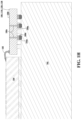
- FIGS. 1 E- 1 H are various views of an example, non-limiting embodiment of a system configuration 140 in accordance with various aspects described herein.
- FIG. 1 E is a perspective view of the system configuration 140
- FIG. 1 F is a partial perspective cross-sectional view of the system configuration 140 (e.g., taken along a plane that extends from dotted line 142 of FIG. 1 E in the y-direction)
- FIG. 1 G is an expanded view of a portion 144 shown in FIG. 1 F
- FIG. 1 H is a cross-sectional view of the system configuration 140 (e.g., taken along a plane that extends from dotted line 142 of FIG. 1 E in the y-direction).
- FIGS. 1 E is a perspective view of the system configuration 140
- FIG. 1 F is a partial perspective cross-sectional view of the system configuration 140 (e.g., taken along a plane that extends from dotted line 142 of FIG. 1 E in the y-direction)
- FIGS. 1 E- 1 H are made in reference to the system configuration 100 of FIG. 1 A . However, it is to be understood and appreciated that some or all of the features shown in any of FIGS. 1 E- 1 H may apply to any of the risers 116 / 126 / 136 of system configurations 110 / 120 / 130 .
- a riser substrate 106 r may be coated with a surface layering (not shown).
- the surface layering may be composed of polyimide and/or any other suitable type of material.
- the through riser vias 106 v may be formed or etched via lithography.
- Other techniques may be employed to form the through riser vias 106 v if the riser substrate 106 r is composed of a different type of material. For instance, where the riser substrate 106 r is composed of ceramic material, the through riser vias 106 v may be formed via mechanical drilling and/or the like.
- the riser substrate 106 r (having the surface layering thereon) may be heated so as to develop a thermal oxide that traverses all surfaces of the riser substrate 106 r , including throughout the etched vias 106 v .
- the thermal oxide provides an insulating effect for the riser substrate 106 r .
- the through riser vias 106 v may then each be partially or fully filled with an electrically conductive material, such as copper, tungsten, aluminum, gold, and/or the like. Referring to FIGS.
- redistribution layer 106 t (e.g., composed of individual copper plates, thus forming RDL 1 of copper contacts) may be aligned with the through riser vias 106 v and disposed on the top surface of the riser substrate 106 r so as to respectively couple with the through riser vias 106 v . Portions of the redistribution layer 106 t may be wire bonded ( 105 ) to electrical interface pads 104 c on the device (e.g., integrated circuit) 104 . The device 104 may be affixed to the substrate 102 via adhesive material 104 a .
- redistribution layer 106 b (e.g., composed of individual copper plates, thus forming RDL 2 of copper contacts) may be aligned with and coupled to the pillars 106 p on the bottom surface of the riser substrate 106 r .
- the pillars 106 p may interface with the substrate 102 via solder 106 e and substrate pads 102 p (e.g., metal, such as copper).
- differential lines may be disposed through vias within the substrate 102 and extend to a top surface of the substrate 102 so as to engage with the pillars 106 p.
- FIGS. 1 I and 1 J are perspective and cross-sectional views of a different system configured using wire bonding without a riser (or RF interconnect configuration), such as that as described herein.
- the wire bonds in the latter construction are much longer (given the lack of a riser, such as the riser 106 / 116 / 126 / 136 ), which can undesirably lead to increased inductance, thereby negatively impacting high frequency operations.
- FIG. 1 K illustrates different units of through riser vias in accordance with various aspects described herein.
- Inductance over the wire bond(s) described above with respect to any of FIGS. 1 A- 1 H can be adjusted, or otherwise controlled, by selecting different dimensions for the through riser vias.
- a larger through riser via can reduce the inductance, although aspect ratio limitations apply. That is, while the diameter of a through riser via relative to a height of the riser substrate can be increased, the riser substrate itself generally cannot be made infinitely thick. To address the inductance issue, therefore, multiple through riser vias can be provided in a given riser in accordance with a minimum spacing design rule.
- the through riser vias may be positioned such that their centers are separated from one another by no less than a threshold distance (e.g., one times (1 ⁇ ) the diameter of the via, such as, for instance, 20 um). It has been shown that the addition of a second or third through riser via in a riser substrate can reduce the inductance by two times, three times, or more.
- a threshold distance e.g., one times (1 ⁇ ) the diameter of the via, such as, for instance, 20 um.
- FIG. 1 L is a graphical representation that illustrates various losses (across frequency) exhibited by a system configuration that employs a riser as compared to losses exhibited by a system configuration that employs traditional wire bonds without the use of such a riser.
- S 11 , S 21 , S 12 , and S 22 shown in FIG. 1 L relate to a scattering matrix that represents what happens to an incoming wave, how much of that incoming wave makes it through, and how much of that incoming wave is reflected.
- losses across frequency are generally lower for a system configuration that employs a riser.
- the signal path through an organic substrate, pillars, and through riser vias to a redistribution layer generally yields lower losses at up to 120 GHz data speeds.
- a desired interface would have ⁇ 1 dB loss ( ⁇ 80% power delivered) and return loss of less than-10 dB ( ⁇ 10% power reflected). It is to be understood and appreciated that various material systems, geometries, and wire bond lengths can be used, with a goal for as much transparency as possible, e.g., loss ⁇ 0 dB and return loss of ⁇ (minus infinity).
- height mismatching between a riser and a device can be adjusted or selected based on the technique to be used for wire bonding of the two components and/or based on a desired inductance over the wire bond(s). For instance, where a ball and stitch bond technique is to be employed, and thus geometric characteristics include a small ball formed on the departure bond, an optional ball on the destination bond, and a circular wire section, the dimensions of the riser may be defined such that the height of the riser is slightly lower than the height of the device when both components are positioned and coupled onto a substrate. In one or more embodiments, the difference in height between the riser and the device (where either one can be taller than the other) can be at least about 25 um.
- the difference in height can be at least about 100 um.
- Having a height mismatch may compensate for a vertical lift off required when using a ball and stitch (e.g., axisymmetric, narrow, and/or deep reaching) arc capillary wire bonder.
- a metal e.g., gold
- a metal wire may pass through a hollow center of the arc capillary and may, at a tip portion of the arc capillary, be melted into a ball.
- the arc capillary may be struck onto a surface of the first component (e.g., the riser or the device), where an ultrasonic action may scrub the metal ball onto the riser for adhesion.
- FIG. 1 M illustrates example height mismatches between two components as well as corresponding resulting ball and stitch wire bonds formed using an arc capillary of particular dimensions in accordance with various aspects described herein.
- FIG. 1 N illustrates an example of a ball and stitch wire bond where there is no height mismatch between two components in accordance with various aspects described herein.
- having an exact height match between the two components does not necessarily provide the benefit of a shortened wire bond.
- the ball and stitch bond technique requires a rising phase, although the tool can be moved in either direction—rising, neutral, or dropping.
- a “flat” short connection is generally not possible, and thus a resulting wire bond might be longer.
- the dimensions of the riser may be defined such that the height of the riser is about (or exactly) equal to the height of the device when both components are positioned and coupled onto a substrate.
- the difference in height between the riser and the device can be no more than about 25 um.
- FIG. 1 O illustrates example wedge bond loop profiles and lengths and an example wedge bond tool in accordance with various aspects described herein. In terms of tool movement, there is a minimal rising phase and almost a “flat” short connection.
- the tool cannot be moved in both directions-rising or neutral, which can limit the compliance to height variability.
- the resulting wire bond may be shorter than in a case where a ball and stitch technique is used, although handling of a (e.g., asymmetric) wedge (or wire clamp) bonding tool may be more complex due to its larger size, its narrowness in only one direction, and the different clearance requirements on departure and destination.
- FIG. 2 depicts an illustrative embodiment of a method 200 in accordance with various aspects described herein.
- the method can include mounting a riser over a first portion of a substrate, the riser being configured with one or more through riser vias for coupling to an interconnect of the substrate.
- the method may include mounting the riser 106 over a first portion of the substrate 102 , the riser 106 being configured with one or more through riser vias 106 v for coupling to an interconnect 102 i of the substrate 102 .
- the method can include securing a device over a second portion of the substrate, the device having one or more conductive contacts residing in a plane of the device.
- the method may include securing the device 104 over a second portion of the substrate 102 , the device 104 having one or more conductive contacts 104 c residing in a plane of the device 104 .
- the method can include providing one or more wire bonds that couple the one or more through riser vias with the one or more conductive contacts thereby enabling connectivity of the interconnect to be raised relative to the plane of the device such that at least one of the one or more wire bonds has a length that is less than a threshold length.
- the method can include providing one or more wire bonds 105 that couple the one or more through riser vias 106 v with the one or more conductive contacts 104 c thereby enabling connectivity of the interconnect 102 i to be raised relative to the plane of the device 104 such that at least one of the one or more wire bonds 105 has a length that is less than a threshold length.
- the threshold length may be based on a desired/target (e.g., reduced or minimum) signal loss amount and/or a desired/target (e.g., reduced or minimum) inductance/capacitance over a given wire bond.
- the riser comprises at least one of an integrated passive device or one or more passive surface mount devices.
- the riser comprises at least one of an active device or one or more passive surface mount devices.
- first is for clarity only and does not otherwise indicate or imply any order in time. For instance, “a first determination,” “a second determination,” and “a third determination,” does not indicate or imply that the first determination is to be made before the second determination, or vice versa, etc.
- the memory components described herein can be either volatile memory or nonvolatile memory, or can comprise both volatile and nonvolatile memory, by way of illustration, and not limitation, volatile memory, non-volatile memory, disk storage, and memory storage.
- nonvolatile memory can be included in read only memory (ROM), programmable ROM (PROM), electrically programmable ROM (EPROM), electrically erasable ROM (EEPROM), or flash memory.
- Volatile memory can comprise random access memory (RAM), which acts as external cache memory.
- RAM is available in many forms such as synchronous RAM (SRAM), dynamic RAM (DRAM), synchronous DRAM (SDRAM), double data rate SDRAM (DDR SDRAM), enhanced SDRAM (ESDRAM), Synchlink DRAM (SLDRAM), and direct Rambus RAM (DRRAM).
- SRAM synchronous RAM
- DRAM dynamic RAM
- SDRAM synchronous DRAM
- DDR SDRAM double data rate SDRAM
- ESDRAM enhanced SDRAM
- SLDRAM Synchlink DRAM
- DRRAM direct Rambus RAM
- the disclosed memory components of systems or methods herein are intended to comprise, without being limited to comprising, these and any other suitable types of memory.
- the disclosed subject matter can involve or be practiced or associated with any type of computer system configuration, comprising single-processor or multiprocessor computer systems, mini-computing devices, mainframe computers, as well as personal computers, hand-held computing devices (e.g., PDA, phone, smartphone, watch, tablet computers, netbook computers, etc.), microprocessor-based or programmable consumer or industrial electronics, and the like.
- the illustrated aspects can also involve or be associated with/practiced in distributed computing environments where tasks are performed by remote processing devices that are linked through a communications network; however, some if not all aspects of the subject disclosure can be practiced on stand-alone computers.
- program modules can be located in both local and remote memory storage devices.
- the terms “component,” “system” and the like are intended to refer to, or comprise, a computer-related entity or an entity related to an operational apparatus with one or more specific functionalities, wherein the entity can be either hardware, a combination of hardware and software, software, or software in execution.
- a component may be, but is not limited to being, a process running on a processor, a processor, an object, an executable, a thread of execution, computer-executable instructions, a program, and/or a computer.
- an application running on a server and the server can be a component.
- One or more components may reside within a process and/or thread of execution and a component may be localized on one computer and/or distributed between two or more computers. In addition, these components can execute from various computer readable media having various data structures stored thereon. The components may communicate via local and/or remote processes such as in accordance with a signal having one or more data packets (e.g., data from one component interacting with another component in a local system, distributed system, and/or across a network such as the Internet with other systems via the signal).
- a signal having one or more data packets (e.g., data from one component interacting with another component in a local system, distributed system, and/or across a network such as the Internet with other systems via the signal).
- a component can be an apparatus with specific functionality provided by mechanical parts operated by electric or electronic circuitry, which is operated by a software or firmware application executed by a processor, wherein the processor can be internal or external to the apparatus and executes at least a part of the software or firmware application.
- a component can be an apparatus that provides specific functionality through electronic components without mechanical parts, the electronic components can comprise a processor therein to execute software or firmware that confers at least in part the functionality of the electronic components. While various components have been illustrated as separate components, it will be appreciated that multiple components can be implemented as a single component, or a single component can be implemented as multiple components, without departing from example embodiments.
- one or more embodiments can be implemented as a method, apparatus or article of manufacture using standard programming and/or engineering techniques to produce software, firmware, hardware or any combination thereof to control a computer to implement the disclosed subject matter.
- article of manufacture as used herein is intended to encompass a computer program accessible from any computer-readable device or computer-readable storage/communications media.
- computer readable storage media can include, but are not limited to, magnetic storage devices (e.g., hard disk, floppy disk, magnetic strips), optical disks (e.g., compact disk (CD), digital versatile disk (DVD)), smart cards, and flash memory devices (e.g., card, stick, key drive).
- magnetic storage devices e.g., hard disk, floppy disk, magnetic strips
- optical disks e.g., compact disk (CD), digital versatile disk (DVD)
- smart cards e.g., card, stick, key drive
- example and exemplary are used herein to mean serving as an instance or illustration. Any embodiment or design described herein as “example” or “exemplary” is not necessarily to be construed as preferred or advantageous over other embodiments or designs. Rather, use of the word example or exemplary is intended to present concepts in a concrete fashion.
- the term “or” is intended to mean an inclusive “or” rather than an exclusive “or”. That is, unless specified otherwise or clear from context, “X employs A or B” is intended to mean any of the natural inclusive permutations.
- processor can refer to substantially any computing processing unit or device comprising, but not limited to comprising, single-core processors; single-processors with software multithread execution capability; multi-core processors; multi-core processors with software multithread execution capability; multi-core processors with hardware multithread technology; parallel platforms; and parallel platforms with distributed shared memory.
- a processor can refer to an integrated circuit, an application specific integrated circuit (ASIC), a digital signal processor (DSP), a field programmable gate array (FPGA), a programmable logic controller (PLC), a complex programmable logic device (CPLD), a discrete gate or transistor logic, discrete hardware components or any combination thereof designed to perform the functions described herein.
- ASIC application specific integrated circuit
- DSP digital signal processor
- FPGA field programmable gate array
- PLC programmable logic controller
- CPLD complex programmable logic device
- processors can exploit nano-scale architectures such as, but not limited to, molecular and quantum-dot based transistors, switches and gates, in order to optimize space usage or enhance performance of user equipment.
- a processor can also be implemented as a combination of computing processing units.
- a flow diagram may include a “start” and/or “continue” indication.
- the “start” and “continue” indications reflect that the steps presented can optionally be incorporated in or otherwise used in conjunction with other routines.
- start indicates the beginning of the first step presented and may be preceded by other activities not specifically shown.
- continue indicates that the steps presented may be performed multiple times and/or may be succeeded by other activities not specifically shown.
- a flow diagram indicates a particular ordering of steps, other orderings are likewise possible provided that the principles of causality are maintained.
- the term(s) “operably coupled to”, “coupled to”, and/or “coupling” includes direct coupling between items and/or indirect coupling between items via one or more intervening items.
- Such items and intervening items include, but are not limited to, junctions, communication paths, components, circuit elements, circuits, functional blocks, and/or devices.
- indirect coupling a signal conveyed from a first item to a second item may be modified by one or more intervening items by modifying the form, nature or format of information in a signal, while one or more elements of the information in the signal are nevertheless conveyed in a manner than can be recognized by the second item.
- an action in a first item can cause a reaction on the second item, as a result of actions and/or reactions in one or more intervening items.
Landscapes
- Engineering & Computer Science (AREA)
- Microelectronics & Electronic Packaging (AREA)
- Power Engineering (AREA)
- Computer Hardware Design (AREA)
- Physics & Mathematics (AREA)
- Condensed Matter Physics & Semiconductors (AREA)
- General Physics & Mathematics (AREA)
- Wire Bonding (AREA)
- Manufacturing & Machinery (AREA)
- Ceramic Engineering (AREA)
Abstract
Description
- The subject disclosure relates to an RF interconnect configuration for a substrate and a surface mount device.
- Devices, such as electro-optic transmitters, such as Mach-Zehnder modulators, or opto-electric receivers, such as Intradyne Coherent Receiver (ICR) chips, are typically electrically coupled to a substrate via wire bonding. This provides an RF connection between the optical device and the substrate for data signal transfer.
- Reference will now be made to the accompanying drawings, which are not necessarily drawn to scale, and wherein:
-
FIG. 1A is a block diagram illustrating an example, non-limiting embodiment of a system configuration in accordance with various aspects described herein. -
FIGS. 1B-1D are block diagrams illustrating other example, non-limiting embodiments of the system configuration in accordance with various aspects described herein. -
FIGS. 1E-1H are various views of an example, non-limiting embodiment of a system configuration in accordance with various aspects described herein. -
FIGS. 1I and 1J are perspective and cross-sectional views of a different system configured using wire bonding without a riser (or RF interconnect configuration), such as that as described herein. -
FIG. 1K illustrates different units of through riser vias in accordance with various aspects described herein. -
FIG. 1L is a graphical representation that illustrates various losses (across frequency) exhibited by a system configuration that employs a riser as compared to losses exhibited by a system configuration that employs traditional wire bonds without the use of such a riser. -
FIG. 1M illustrates example height mismatches between two components as well as corresponding resulting ball and stitch wire bonds formed using an arc capillary of particular dimensions in accordance with various aspects described herein. -
FIG. 1N illustrates an example of a ball and stitch wire bond where there is no height mismatch between two components in accordance with various aspects described herein. -
FIG. 1O illustrates example wedge bond loop profiles and lengths and an example wedge bond tool in accordance with various aspects described herein. -
FIG. 2 depicts an illustrative embodiment of a method in accordance with various aspects described herein. - In a high frequency application space (e.g., 65 gigahertz (GHz) or higher), wire bonds that are too physically long can lead to increased inductance, which can “choke” (or negatively impact) the high frequency data. Long wire bonds can also contribute to degraded channel to channel isolation, i.e. crosstalk between neighboring channels. Typically, transmitters and receivers are configured in quads or octals (i.e., Quad Parallel Mach-Zehnder (QPMZ)), where these arrays of transmitters and receivers are on a 450 micron (um), 500 um, or 625 um channel pitch. To achieve lower manufacturing costs of pluggable transceivers as well as improved throughput (i.e., increased parallelization or Baud rate), the hierarchy within devices is becoming more flattened. Turning a pluggable device into an optical configuration in this way can eliminate discrete optical-to-electrical (O-E)/electrical-to-optical (E-O) packages. This does not come without challenges, however, since, in the case of a transmitter thin-film lithium niobate (TFLN) modulator, the modulator must be directly interfaced to a transceiver printed circuit board (PCB) as opposed to being implemented in its own package with interfaces via pins or a flex.
- An existing technique involves simply mounting a transmitter TFLN modulator onto a top surface of a PCB. This unfortunately results in prohibitively long wire bonds for high frequency and high Baud operation.
- Another technique is to use controlled-depth mechanical or laser routing where several top layers of dielectric and metal are removed from the PCB while preserving the PCB backside real estate. The challenge with this technique is the difficulty in accurately routing the edges. Particularly, the edge of die becomes “pushed away” from the transmitter TFLN modulator and thus similarly results in prohibitively long wire bonds for high frequency and high Baud operation. For instance, in a case where the slope of the edge is about 15 degrees and the wire bond pad registration tolerance is about ±50 microns (um), the wire bond length can be larger as compared to other conventional interfaces by more than a hundred microns.
- As another option, the transmitter TFLN modulator may be positioned in a cut-out of a PCB transceiver board and wire bonded directly to the board. However, the repercussions of such an interfacing technique is that a large cut-out is required as well as fine precision mechanical routing in order for the bonding wires to be as short as possible for high frequency operation. Such routing through a cavity also reduces the available real estate on the backside of the transceiver PCB, which significantly reduces the available space for supporting electronics, especially in the context of tunable coherent optics which are considerably more complex than fixed wavelength intensity modulation (IM)/direct detection (DD).
- The subject disclosure describes, among other things, illustrative embodiments of an interconnect scheme in which an RF interconnect for a surface mount or flip-chip integrated passive or active device is raised toward or to the plane of a surface mount E-O or O-E transmitter or receiver so as to enable short wire bonds (or, in other words, wire bonds of limited physical length). In exemplary embodiments, the interconnect scheme may be provided by way of a riser that is bumped on one side to facilitate surface mounting of the riser onto a substrate (e.g., an organic substrate, such as a PCB) or a substrate-like PCB (SLP), and that includes one or more integrated through riser vias that facilitate “raising” of RF from a bottom or underside portion of the substrate toward or to a top side of the surface mount or flip-chip integrated passive or active device, enabling the use of wire bonds of limited physical length.
- The height of the riser may be chosen such that a top surface portion of the riser (e.g., exactly) matches a top plane of the surface mount E-O or O-E transmitter or receiver in height or such that a top surface portion of the riser is slightly higher than or slightly lower than (e.g., within a threshold distance from) a height of the top plane of the surface mount E-O or O-E transmitter or receiver. The choice of the relative heights of the riser and the surface mount E-O or O-E transmitter or receiver may depend at least in part on a desired bonding technique for the wire bonds, as described in more detail below.
- The RF riser may be composed of any suitable material or any material system. For example, the riser may be composed of glass (e.g., high purity fused silica (HPFS), photo imageable/definable glass in the lithium-aluminum silicate family, and/or the like), ceramic material (e.g., high temperature cofired multilayer ceramics (HTCC), low temperature cofired multilayer ceramics (LTCC), thin-film aluminum nitride (AlN), thin-film aluminum oxide (Al2O3), and/or the like), a semiconductor material (e.g., silicon, etc.), active materials/devices (e.g., complementary metal-oxide semiconductor (CMOS), bipolar CMOS (BiCMOS), silicon germanium (SiGe), indium phosphide (InP), gallium arsenide (GaAs), and/or the like), quartz, etc., or a combination of some or all of these materials. Other types of materials or combination of materials can be used to form the riser.
- The riser may include additional passive elements, inductors, capacitors, transformers, transmission lines, and/or any transformations thereof. The riser may additionally, or alternatively, include active devices, such as amplifiers, boosters, and/or the like. In exemplary embodiments, the riser may be composed of a silicon substrate in which through silicon vias (TSVs) are geometrically configured to provide desired impedance throughout the substrate. The riser may additionally, or alternatively, be composed of glass in which through glass vias (TGVs) are geometrically configured. Various implementations or configurations of a riser are described in more detail below. Again, it is to be understood and appreciated that any material system can be used to form the riser.
- Providing an interconnect scheme between a substrate and a surface mount E-O or O-E transmitter or receiver, as described herein, allows for the use of a differential-output driver with E-O crystal Mach-Zehnder modulators (MZMs), which, as compared to single-ended driving of those same modulators, enables improved signal integrity for the traveling wave (TW)-MZM as well as improved signal-to-noise ratio (SNR) and thus better achievable propagation distance or modulation format complexity (i.e., higher throughput). The RF interconnect scheme also helps to de-risk system designs such that certain through silicon vias may be avoided, thus alleviating stress-related issues on optical waveguides, multi-mode interferometers (MMIs), and flip-chips (since there are significant stresses introduced in the metallization and bumps due to the thermal expansion coefficient between silicon and an organic substrate—i.e., 2-3 parts per million (ppm)/° C. versus 20 ppm/° C.). For instance, vias (e.g., TSVs, etc.) can be advantageously avoided in the active device. Additionally, the RF interconnect scheme can allow for the chip to be bonded with a flexible adhesive, which is beneficial as compared to the rigidity of a flip chip attach.
- Exemplary embodiments of the riser allow for patterning of through riser vias (e.g., TSVs in a case where the riser is composed of silicon) such that (e.g., copper) redistribution layers (RDLs) can be employed on both sides of a given through riser via to “massage” (or adjust) a capacitance-inductance-capacitance (CLC) network, thereby improving the bandwidth and return loss beyond what would be achievable solely with wire bonds, especially when the length from ball to stitch or stitch to stich (wedge/wedge) is beyond 150 um and at the limit of tolerancing (i.e., comparing the tolerancing of lithography versus a mechanical wire bonder). It is to be understood and appreciated that the riser may or may not employ (e.g., copper) redistribution layer(s).
- In a case where the riser is an integrated passive device, the capacitance and inductance on both the board side and the wire bond side can be adjusted or customized. Adding additional through riser vias can aid in managing the inductance. Furthermore, transmission lines (e.g., 50 ohm) or any form of RF transformation can be added in between to further adjust or customize the signaling.
- One or more aspects of the subject disclosure include a system. The system may include a substrate having an interconnect in or on a surface of the substrate. The system may also include a riser disposed over the surface, the riser being configured with one or more through riser vias for coupling to the interconnect. The system may also include a device positioned over the surface, the device having one or more conductive contacts residing in a plane of the device. The system may also include one or more wire bonds coupling the one or more through riser vias with the one or more conductive contacts thereby enabling connectivity of the interconnect to be raised toward or to the plane of the device such that at least one of the one or more wire bonds has a limited physical length.
- One or more aspects of the subject disclosure include a riser. The riser may include a body and one or more pillars or solder bumps on an underside of the body for facilitating mounting of the riser to a substrate. Further, the riser may include one or more vias defined in the body and coupled to the one or more pillars or solder bumps, wherein mounting of the riser to the substrate enables connectivity of an interconnect of the substrate to be raised toward or to a plane of a device disposed over the substrate such that a wire bond for electrical coupling of the riser and the device has a length that is less than a threshold length.
- One or more aspects of the subject disclosure include a method. The method may include mounting a riser over a first portion of a substrate, the riser being configured with one or more through riser vias for coupling to an interconnect of the substrate. Further, the method may include securing a device over a second portion of the substrate, the device having one or more conductive contacts residing in a plane of the device. Further, the method may include providing one or more wire bonds that couple the one or more through riser vias with the one or more conductive contacts thereby enabling connectivity of the interconnect to be raised relative to the plane of the device such that at least one of the one or more wire bonds has a length that is less than a threshold length.
- Other embodiments are described in the subject disclosure.
- Referring now to
FIG. 1A , a block diagram is shown illustrating an example, non-limiting embodiment of asystem configuration 100 in accordance with various aspects described herein. Thesystem configuration 100 is implemented with an interconnect scheme in which an RF or electrical interconnect (102 i) of a substrate is raised toward or to a plane of a device, thereby enabling short wire bonding. As shown inFIG. 1A , thesystem configuration 100 may include a substrate/board 102, adevice 104, ariser 106, and one or more processing/driver/memory components 108 disposed on asurface 102 s of thesubstrate 102. Thesubstrate 102 may be an organic substrate, such as a multi-layer laminate/PCB or an SLP. Thedevice 104 may be a photonic chip. For instance, thedevice 104 may be a transmitter E-O modulator (TFLN) or a receiver O-E modulator. Alternatively, thedevice 104 may be another type of device. For example, thedevice 104 may be a trans-impedance amplifier, a sensor, another wire bondable device, or a combination of some or all of these devices. Thedevice 104 may be mounted onto thesubstrate 102 in any suitable manner, such as via an adhesive (e.g., glue) or the like. Thedevice 104 may include contact(s) 104 c (on asurface 104 s) as well as one or more other components, such as, a traveling wave electrode disposed on or coupled to the contact(s) 104 c. As shown inFIG. 1A , wire bond(s) 105 may electrically couple the contact(s) 104 c of thedevice 104 with atop redistribution layer 106 t of theriser 106. - The
riser 106 may be composed of one or more of the materials described above. In exemplary embodiments, theriser 106 may be composed of silicon. As shown inFIG. 1A , theriser 106 may be defined with through riser via(s) 106 v coupled to thetop redistribution layer 106 t and abottom redistribution layer 106 b. Theriser 106 may also include pillar(s) 106 p on an underside of theriser 106. In exemplary embodiments, the pillar(s) 106 p may be composed of copper and/or any other type of electrically conductive material (e.g., tungsten, aluminum, gold, etc.). In various embodiments, theriser 106 may be fabricated with the pillar(s) 106 p. For instance, the pillar(s) 106 p may be “grown” on a bottom surface of theriser 106. In certain embodiments, theriser 106 may alternatively include controlled-collapse chip connect (C4)—i.e., solder bumps—aselements 106 p. As shown inFIG. 1A , theriser 106 may be in the form of an integrated passive device (IPD) that raises the RF plane from theboard 102 toward or to a plane (or height) of thedevice 104. This brings the RF signal toward or to the height of thedevice 104, which enables shorter wire bonds and thus reduced or minimized losses. - In one or more embodiments, the
riser 106 may be configured as a bumped component. For instance, theriser 106 may be configured as a ball grid array (BGA) component for surface mounting (e.g., via soldering) onto thesubstrate 102. This enables assembly of theriser 106 and thesubstrate 102 via a standard pick and place procedure as well as standard refloat processing. It is to be understood and appreciated that system configurations involving risers of other constructions are also possible. -
FIGS. 1B-1D are block diagrams illustrating other example, non-limiting embodiments of the system configuration in accordance with various aspects described herein. Referring toFIG. 1B , asystem configuration 110 may include ariser 116 that is similar to theriser 106 ofFIG. 1A —for instance, theriser 116 may be a bumped IPD with through riser via(s) 116 v. However, theriser 116 may include one or more passive (e.g., surface mount)devices 116 d on the top or back side redistribution layer. Thesystem configuration 120 ofFIG. 1C may include ariser 126 that is similar to therisers riser 126 may include through riser via(s) 126 v (on the top or back and bottom or front side of the riser 126) that couple with the active device. Thesystem configuration 130 ofFIG. 1D may include ariser 136 that is similar to therisers devices 136 d on the top or back side redistribution layer. As shown, theriser 136 may include through riser via(s) 136 v (on the top or back and bottom or front side of the riser 136) that couple with the active device and/or passive device(s) 136 d. - Thus, by way of through riser via(s) in a riser, an
RF interconnect 102 i of the substrate 102 (e.g., driver input) can be raised toward or to a horizontal plane (e.g., driver output) of thedevice 104, thereby enabling short (or the shortest possible) wire bond(s) 105 such that mechanical tolerancing is not (or is less so of) a limiting factor. - It is to be understood and appreciated that a given riser may include any suitable number of through riser vias to suit the purpose and associated components in/on the riser. As some examples, a riser may include a plurality of through riser vias or channels and/or differentials (e.g., a ground-signal ground differential configuration, a ground-signal-signal-ground (GSSG) differential, etc.).
-
FIGS. 1E-1H are various views of an example, non-limiting embodiment of asystem configuration 140 in accordance with various aspects described herein. In particular,FIG. 1E is a perspective view of thesystem configuration 140,FIG. 1F is a partial perspective cross-sectional view of the system configuration 140 (e.g., taken along a plane that extends from dottedline 142 ofFIG. 1E in the y-direction),FIG. 1G is an expanded view of aportion 144 shown inFIG. 1F , andFIG. 1H is a cross-sectional view of the system configuration 140 (e.g., taken along a plane that extends from dottedline 142 ofFIG. 1E in the y-direction). For purposes of simplicity, the descriptions ofFIGS. 1E-1H are made in reference to thesystem configuration 100 ofFIG. 1A . However, it is to be understood and appreciated that some or all of the features shown in any ofFIGS. 1E-1H may apply to any of therisers 116/126/136 ofsystem configurations 110/120/130. - As part of fabricating the
riser 106, ariser substrate 106 r (FIG. 1E ) may be coated with a surface layering (not shown). The surface layering may be composed of polyimide and/or any other suitable type of material. In a case where theriser substrate 106 r is composed of silicon, the throughriser vias 106 v (seeFIG. 1G ) may be formed or etched via lithography. Other techniques may be employed to form the throughriser vias 106 v if theriser substrate 106 r is composed of a different type of material. For instance, where theriser substrate 106 r is composed of ceramic material, the throughriser vias 106 v may be formed via mechanical drilling and/or the like. - Returning to the case where the
riser substrate 106 r is composed of silicon, theriser substrate 106 r (having the surface layering thereon) may be heated so as to develop a thermal oxide that traverses all surfaces of theriser substrate 106 r, including throughout the etchedvias 106 v. Where theriser substrate 106 r is doped, and is thus semiconductive, the thermal oxide provides an insulating effect for theriser substrate 106 r. The throughriser vias 106 v may then each be partially or fully filled with an electrically conductive material, such as copper, tungsten, aluminum, gold, and/or the like. Referring toFIGS. 1G and/or 1H ,redistribution layer 106 t (e.g., composed of individual copper plates, thus formingRDL 1 of copper contacts) may be aligned with the throughriser vias 106 v and disposed on the top surface of theriser substrate 106 r so as to respectively couple with the throughriser vias 106 v. Portions of theredistribution layer 106 t may be wire bonded (105) toelectrical interface pads 104 c on the device (e.g., integrated circuit) 104. Thedevice 104 may be affixed to thesubstrate 102 viaadhesive material 104 a. Although not shown in any ofFIGS. 1E-1H ,redistribution layer 106 b (e.g., composed of individual copper plates, thus formingRDL 2 of copper contacts) may be aligned with and coupled to thepillars 106 p on the bottom surface of theriser substrate 106 r. Thepillars 106 p may interface with thesubstrate 102 viasolder 106 e andsubstrate pads 102 p (e.g., metal, such as copper). Although also not shown in any ofFIGS. 1E-1H , differential lines may be disposed through vias within thesubstrate 102 and extend to a top surface of thesubstrate 102 so as to engage with thepillars 106 p. -
FIGS. 1I and 1J are perspective and cross-sectional views of a different system configured using wire bonding without a riser (or RF interconnect configuration), such as that as described herein. As is apparent from a visual comparison of thewire bonds 105 ofFIGS. 1E and 1H with the wire bonds ofFIGS. 1I and 1J , the wire bonds in the latter construction are much longer (given the lack of a riser, such as theriser 106/116/126/136), which can undesirably lead to increased inductance, thereby negatively impacting high frequency operations. -
FIG. 1K illustrates different units of through riser vias in accordance with various aspects described herein. Inductance over the wire bond(s) described above with respect to any ofFIGS. 1A-1H can be adjusted, or otherwise controlled, by selecting different dimensions for the through riser vias. For instance, a larger through riser via can reduce the inductance, although aspect ratio limitations apply. That is, while the diameter of a through riser via relative to a height of the riser substrate can be increased, the riser substrate itself generally cannot be made infinitely thick. To address the inductance issue, therefore, multiple through riser vias can be provided in a given riser in accordance with a minimum spacing design rule. For instance, the through riser vias may be positioned such that their centers are separated from one another by no less than a threshold distance (e.g., one times (1×) the diameter of the via, such as, for instance, 20 um). It has been shown that the addition of a second or third through riser via in a riser substrate can reduce the inductance by two times, three times, or more. -
FIG. 1L is a graphical representation that illustrates various losses (across frequency) exhibited by a system configuration that employs a riser as compared to losses exhibited by a system configuration that employs traditional wire bonds without the use of such a riser. S11, S21, S12, and S22 shown inFIG. 1L relate to a scattering matrix that represents what happens to an incoming wave, how much of that incoming wave makes it through, and how much of that incoming wave is reflected. As shown inFIG. 1L , losses across frequency are generally lower for a system configuration that employs a riser. In essence, the signal path through an organic substrate, pillars, and through riser vias to a redistribution layer (or through co-planar waveguides on a top RDL that feed into through riser vias to a bottom RDL) generally yields lower losses at up to 120 GHz data speeds. A desired interface would have ˜1 dB loss (˜80% power delivered) and return loss of less than-10 dB (˜10% power reflected). It is to be understood and appreciated that various material systems, geometries, and wire bond lengths can be used, with a goal for as much transparency as possible, e.g., loss ˜0 dB and return loss of −∞ (minus infinity). - It is to be understood and appreciated that, at frequencies above 100 GHz (or above 120 GHz), the inclusion of a riser, as described herein, can provide reduced or minimal losses so long as adjustments are made to design parameter(s) (e.g., the height difference between the riser and the optics/application specific integrated circuit (ASIC) device). Thus, it may be possible to adjust/optimize these parameter(s) to obtain improved/desired wire bond performance.
- It is believed that, in a conventional configuration employing wire bonds without a riser as described herein, crosstalk with or between wire bonds is generally higher than in a configuration that utilizes such a riser. It is also believed that such a conventional configuration would not be able to support tight channel pitches whereas a configuration that utilizes a riser would.
- In exemplary embodiments, height mismatching between a riser and a device can be adjusted or selected based on the technique to be used for wire bonding of the two components and/or based on a desired inductance over the wire bond(s). For instance, where a ball and stitch bond technique is to be employed, and thus geometric characteristics include a small ball formed on the departure bond, an optional ball on the destination bond, and a circular wire section, the dimensions of the riser may be defined such that the height of the riser is slightly lower than the height of the device when both components are positioned and coupled onto a substrate. In one or more embodiments, the difference in height between the riser and the device (where either one can be taller than the other) can be at least about 25 um. In certain embodiments, the difference in height can be at least about 100 um. Having a height mismatch may compensate for a vertical lift off required when using a ball and stitch (e.g., axisymmetric, narrow, and/or deep reaching) arc capillary wire bonder. Particularly, during wire bonding, a metal (e.g., gold) wire may pass through a hollow center of the arc capillary and may, at a tip portion of the arc capillary, be melted into a ball. The arc capillary may be struck onto a surface of the first component (e.g., the riser or the device), where an ultrasonic action may scrub the metal ball onto the riser for adhesion. The arc capillary may then be lifted off from the first component and brought over to the second component (e.g., the device or the riser). By virtue of the slight height mismatch between the two components, sufficient vertical spacing permits for the lift off of the arc capillary, thus allowing for the metal wire to form generally upwardly and then sideways. Forming a ball and stitch wire bond without such a height mismatch could risk damaging the metal wire during sideways traversal of the arc capillary from the first component to the second component.
FIG. 1M illustrates example height mismatches between two components as well as corresponding resulting ball and stitch wire bonds formed using an arc capillary of particular dimensions in accordance with various aspects described herein.FIG. 1N illustrates an example of a ball and stitch wire bond where there is no height mismatch between two components in accordance with various aspects described herein. As can be seen from a comparison of the profiles ofFIG. 1M and the profile ofFIG. 1N , having an exact height match between the two components (and even if the wire bond is successfully formed without damage) does not necessarily provide the benefit of a shortened wire bond. In any case, the ball and stitch bond technique requires a rising phase, although the tool can be moved in either direction—rising, neutral, or dropping. Also, a “flat” short connection is generally not possible, and thus a resulting wire bond might be longer. - In a different case where a wedge bond technique is to be employed, and thus geometric characteristics include a smaller departure rectangular pad, a longer pad on the destination bond due to cutting, and a circular wire section, the dimensions of the riser may be defined such that the height of the riser is about (or exactly) equal to the height of the device when both components are positioned and coupled onto a substrate. In one or more embodiments, the difference in height between the riser and the device (where either one can be taller than the other) can be no more than about 25 um.
FIG. 1O illustrates example wedge bond loop profiles and lengths and an example wedge bond tool in accordance with various aspects described herein. In terms of tool movement, there is a minimal rising phase and almost a “flat” short connection. However, the tool cannot be moved in both directions-rising or neutral, which can limit the compliance to height variability. In any case, the resulting wire bond may be shorter than in a case where a ball and stitch technique is used, although handling of a (e.g., asymmetric) wedge (or wire clamp) bonding tool may be more complex due to its larger size, its narrowness in only one direction, and the different clearance requirements on departure and destination. -
FIG. 2 depicts an illustrative embodiment of amethod 200 in accordance with various aspects described herein. - At 202, the method can include mounting a riser over a first portion of a substrate, the riser being configured with one or more through riser vias for coupling to an interconnect of the substrate. For example, the method may include mounting the
riser 106 over a first portion of thesubstrate 102, theriser 106 being configured with one or more throughriser vias 106 v for coupling to aninterconnect 102 i of thesubstrate 102. - At 204, the method can include securing a device over a second portion of the substrate, the device having one or more conductive contacts residing in a plane of the device. For example, the method may include securing the
device 104 over a second portion of thesubstrate 102, thedevice 104 having one or moreconductive contacts 104 c residing in a plane of thedevice 104. - At 206, the method can include providing one or more wire bonds that couple the one or more through riser vias with the one or more conductive contacts thereby enabling connectivity of the interconnect to be raised relative to the plane of the device such that at least one of the one or more wire bonds has a length that is less than a threshold length. For example, the method can include providing one or
more wire bonds 105 that couple the one or more throughriser vias 106 v with the one or moreconductive contacts 104 c thereby enabling connectivity of theinterconnect 102 i to be raised relative to the plane of thedevice 104 such that at least one of the one ormore wire bonds 105 has a length that is less than a threshold length. Because the inductance and/or capacitance associated with the wire bond(s), and thus signal loss in the system, may depend on the length(s) of the wire bond(s), in one or more embodiments, the threshold length may be based on a desired/target (e.g., reduced or minimum) signal loss amount and/or a desired/target (e.g., reduced or minimum) inductance/capacitance over a given wire bond. Further, in one or more embodiments, the riser comprises at least one of an integrated passive device or one or more passive surface mount devices. Furthermore, in one or more embodiments, the riser comprises at least one of an active device or one or more passive surface mount devices. - While for purposes of simplicity of explanation, the respective processes are shown and described as a series of blocks in
FIG. 2 , it is to be understood and appreciated that the claimed subject matter is not limited by the order of the blocks, as some blocks may occur in different orders and/or concurrently with other blocks from what is depicted and described herein. Moreover, not all illustrated blocks may be required to implement the methods described herein. - The terms “first,” “second,” “third,” and so forth, as may be used in the claims, unless otherwise clear by context, is for clarity only and does not otherwise indicate or imply any order in time. For instance, “a first determination,” “a second determination,” and “a third determination,” does not indicate or imply that the first determination is to be made before the second determination, or vice versa, etc.
- In the subject specification, terms such as “store,” “storage,” “data store,” data storage,” “database,” and substantially any other information storage component relevant to operation and functionality of a component, refer to “memory components,” or entities embodied in a “memory” or components comprising the memory. It will be appreciated that the memory components described herein can be either volatile memory or nonvolatile memory, or can comprise both volatile and nonvolatile memory, by way of illustration, and not limitation, volatile memory, non-volatile memory, disk storage, and memory storage. Further, nonvolatile memory can be included in read only memory (ROM), programmable ROM (PROM), electrically programmable ROM (EPROM), electrically erasable ROM (EEPROM), or flash memory. Volatile memory can comprise random access memory (RAM), which acts as external cache memory. By way of illustration and not limitation, RAM is available in many forms such as synchronous RAM (SRAM), dynamic RAM (DRAM), synchronous DRAM (SDRAM), double data rate SDRAM (DDR SDRAM), enhanced SDRAM (ESDRAM), Synchlink DRAM (SLDRAM), and direct Rambus RAM (DRRAM). Additionally, the disclosed memory components of systems or methods herein are intended to comprise, without being limited to comprising, these and any other suitable types of memory.
- Moreover, it will be noted that the disclosed subject matter can involve or be practiced or associated with any type of computer system configuration, comprising single-processor or multiprocessor computer systems, mini-computing devices, mainframe computers, as well as personal computers, hand-held computing devices (e.g., PDA, phone, smartphone, watch, tablet computers, netbook computers, etc.), microprocessor-based or programmable consumer or industrial electronics, and the like. The illustrated aspects can also involve or be associated with/practiced in distributed computing environments where tasks are performed by remote processing devices that are linked through a communications network; however, some if not all aspects of the subject disclosure can be practiced on stand-alone computers. In a distributed computing environment, program modules can be located in both local and remote memory storage devices.
- As used in some contexts in this application, in some embodiments, the terms “component,” “system” and the like are intended to refer to, or comprise, a computer-related entity or an entity related to an operational apparatus with one or more specific functionalities, wherein the entity can be either hardware, a combination of hardware and software, software, or software in execution. As an example, a component may be, but is not limited to being, a process running on a processor, a processor, an object, an executable, a thread of execution, computer-executable instructions, a program, and/or a computer. By way of illustration and not limitation, both an application running on a server and the server can be a component. One or more components may reside within a process and/or thread of execution and a component may be localized on one computer and/or distributed between two or more computers. In addition, these components can execute from various computer readable media having various data structures stored thereon. The components may communicate via local and/or remote processes such as in accordance with a signal having one or more data packets (e.g., data from one component interacting with another component in a local system, distributed system, and/or across a network such as the Internet with other systems via the signal). As another example, a component can be an apparatus with specific functionality provided by mechanical parts operated by electric or electronic circuitry, which is operated by a software or firmware application executed by a processor, wherein the processor can be internal or external to the apparatus and executes at least a part of the software or firmware application. As yet another example, a component can be an apparatus that provides specific functionality through electronic components without mechanical parts, the electronic components can comprise a processor therein to execute software or firmware that confers at least in part the functionality of the electronic components. While various components have been illustrated as separate components, it will be appreciated that multiple components can be implemented as a single component, or a single component can be implemented as multiple components, without departing from example embodiments.
- Further, one or more embodiments can be implemented as a method, apparatus or article of manufacture using standard programming and/or engineering techniques to produce software, firmware, hardware or any combination thereof to control a computer to implement the disclosed subject matter. The term “article of manufacture” as used herein is intended to encompass a computer program accessible from any computer-readable device or computer-readable storage/communications media. For example, computer readable storage media can include, but are not limited to, magnetic storage devices (e.g., hard disk, floppy disk, magnetic strips), optical disks (e.g., compact disk (CD), digital versatile disk (DVD)), smart cards, and flash memory devices (e.g., card, stick, key drive). Of course, those skilled in the art will recognize many modifications can be made to this configuration without departing from the scope or spirit of the various embodiments.
- In addition, the words “example” and “exemplary” are used herein to mean serving as an instance or illustration. Any embodiment or design described herein as “example” or “exemplary” is not necessarily to be construed as preferred or advantageous over other embodiments or designs. Rather, use of the word example or exemplary is intended to present concepts in a concrete fashion. As used in this application, the term “or” is intended to mean an inclusive “or” rather than an exclusive “or”. That is, unless specified otherwise or clear from context, “X employs A or B” is intended to mean any of the natural inclusive permutations. That is, if X employs A; X employs B; or X employs both A and B, then “X employs A or B” is satisfied under any of the foregoing instances. In addition, the articles “a” and “an” as used in this application and the appended claims should generally be construed to mean “one or more” unless specified otherwise or clear from context to be directed to a singular form.
- As may be employed herein, the term “processor” can refer to substantially any computing processing unit or device comprising, but not limited to comprising, single-core processors; single-processors with software multithread execution capability; multi-core processors; multi-core processors with software multithread execution capability; multi-core processors with hardware multithread technology; parallel platforms; and parallel platforms with distributed shared memory. Additionally, a processor can refer to an integrated circuit, an application specific integrated circuit (ASIC), a digital signal processor (DSP), a field programmable gate array (FPGA), a programmable logic controller (PLC), a complex programmable logic device (CPLD), a discrete gate or transistor logic, discrete hardware components or any combination thereof designed to perform the functions described herein. Processors can exploit nano-scale architectures such as, but not limited to, molecular and quantum-dot based transistors, switches and gates, in order to optimize space usage or enhance performance of user equipment. A processor can also be implemented as a combination of computing processing units.
- As may be used herein, terms such as “data storage,” data storage,” “database,” and substantially any other information storage component relevant to operation and functionality of a component, refer to “memory components,” or entities embodied in a “memory” or components comprising the memory. It will be appreciated that the memory components or computer-readable storage media, described herein can be either volatile memory or nonvolatile memory or can include both volatile and nonvolatile memory.
- What has been described above includes mere examples of various embodiments. It is, of course, not possible to describe every conceivable combination of components or methodologies for purposes of describing these examples, but one of ordinary skill in the art can recognize that many further combinations and permutations of the present embodiments are possible. Accordingly, the embodiments disclosed and/or claimed herein are intended to embrace all such alterations, modifications and variations that fall within the spirit and scope of the appended claims. Furthermore, to the extent that the term “includes” is used in either the detailed description or the claims, such term is intended to be inclusive in a manner similar to the term “comprising” as “comprising” is interpreted when employed as a transitional word in a claim.
- In addition, a flow diagram may include a “start” and/or “continue” indication. The “start” and “continue” indications reflect that the steps presented can optionally be incorporated in or otherwise used in conjunction with other routines. In this context, “start” indicates the beginning of the first step presented and may be preceded by other activities not specifically shown. Further, the “continue” indication reflects that the steps presented may be performed multiple times and/or may be succeeded by other activities not specifically shown. Further, while a flow diagram indicates a particular ordering of steps, other orderings are likewise possible provided that the principles of causality are maintained.
- As may also be used herein, the term(s) “operably coupled to”, “coupled to”, and/or “coupling” includes direct coupling between items and/or indirect coupling between items via one or more intervening items. Such items and intervening items include, but are not limited to, junctions, communication paths, components, circuit elements, circuits, functional blocks, and/or devices. As an example of indirect coupling, a signal conveyed from a first item to a second item may be modified by one or more intervening items by modifying the form, nature or format of information in a signal, while one or more elements of the information in the signal are nevertheless conveyed in a manner than can be recognized by the second item. In a further example of indirect coupling, an action in a first item can cause a reaction on the second item, as a result of actions and/or reactions in one or more intervening items.
- Although specific embodiments have been illustrated and described herein, it should be appreciated that any arrangement which achieves the same or similar purpose may be substituted for the embodiments described or shown by the subject disclosure. The subject disclosure is intended to cover any and all adaptations or variations of various embodiments. Combinations of the above embodiments, and other embodiments not specifically described herein, can be used in the subject disclosure. For instance, one or more features from one or more embodiments can be combined with one or more features of one or more other embodiments. In one or more embodiments, features that are positively recited can also be negatively recited and excluded from the embodiment with or without replacement by another structural and/or functional feature. The steps or functions described with respect to the embodiments of the subject disclosure can be performed in any order. The steps or functions described with respect to the embodiments of the subject disclosure can be performed alone or in combination with other steps or functions of the subject disclosure, as well as from other embodiments or from other steps that have not been described in the subject disclosure. Further, more than or less than all of the features described with respect to an embodiment can also be utilized.
Claims (20)
Priority Applications (4)
| Application Number | Priority Date | Filing Date | Title |
|---|---|---|---|
| US18/177,805 US20240297105A1 (en) | 2023-03-03 | 2023-03-03 | Radio frequency (rf) interconnect configuration for substrate and surface mount device |
| CN202480025273.3A CN121039791A (en) | 2023-03-03 | 2024-02-29 | Radio frequency (RF) interconnect configurations for substrates and surface mount devices |
| EP24714707.7A EP4533525A1 (en) | 2023-03-03 | 2024-02-29 | Radio frequency (rf) interconnect configuration for substrate and surface mount device |
| PCT/US2024/017839 WO2024186569A1 (en) | 2023-03-03 | 2024-02-29 | Radio frequency (rf) interconnect configuration for substrate and surface mount device |
Applications Claiming Priority (1)
| Application Number | Priority Date | Filing Date | Title |
|---|---|---|---|
| US18/177,805 US20240297105A1 (en) | 2023-03-03 | 2023-03-03 | Radio frequency (rf) interconnect configuration for substrate and surface mount device |
Publications (1)
| Publication Number | Publication Date |
|---|---|
| US20240297105A1 true US20240297105A1 (en) | 2024-09-05 |
Family
ID=90482367
Family Applications (1)
| Application Number | Title | Priority Date | Filing Date |
|---|---|---|---|
| US18/177,805 Pending US20240297105A1 (en) | 2023-03-03 | 2023-03-03 | Radio frequency (rf) interconnect configuration for substrate and surface mount device |
Country Status (4)
| Country | Link |
|---|---|
| US (1) | US20240297105A1 (en) |
| EP (1) | EP4533525A1 (en) |
| CN (1) | CN121039791A (en) |
| WO (1) | WO2024186569A1 (en) |
Family Cites Families (2)
| Publication number | Priority date | Publication date | Assignee | Title |
|---|---|---|---|---|
| US12074123B2 (en) * | 2020-04-03 | 2024-08-27 | Macom Technology Solutions Holdings, Inc. | Multi level radio frequency (RF) integrated circuit components including passive devices |
| US11830798B2 (en) * | 2021-03-22 | 2023-11-28 | Advanced Semiconductor Engineering, Inc. | Semiconductor device package |
-
2023
- 2023-03-03 US US18/177,805 patent/US20240297105A1/en active Pending
-
2024
- 2024-02-29 CN CN202480025273.3A patent/CN121039791A/en active Pending
- 2024-02-29 WO PCT/US2024/017839 patent/WO2024186569A1/en not_active Ceased
- 2024-02-29 EP EP24714707.7A patent/EP4533525A1/en active Pending
Also Published As
| Publication number | Publication date |
|---|---|
| EP4533525A1 (en) | 2025-04-09 |
| CN121039791A (en) | 2025-11-28 |
| WO2024186569A1 (en) | 2024-09-12 |
Similar Documents
| Publication | Publication Date | Title |
|---|---|---|
| US11824029B2 (en) | Semiconductor package structure | |
| US11409063B2 (en) | Optical interposer | |
| US20210265331A1 (en) | Direct-bonded optoelectronic interconnect for high-density integrated photonics | |
| WO2025006616A1 (en) | Directly bonded optical components | |
| US20170261708A1 (en) | Compact optical transceiver by hybrid multichip integration | |
| US20120207426A1 (en) | Flip-chip packaging for dense hybrid integration of electrical and photonic integrated circuits | |
| JP7782215B2 (en) | quantum devices | |
| TW202235934A (en) | Package and semiconductor device and method for forming the same | |
| US12105323B2 (en) | Semiconductor package | |
| US20240297105A1 (en) | Radio frequency (rf) interconnect configuration for substrate and surface mount device | |
| KR20230130634A (en) | Package containing board and interconnect devices configured for diagonal routing | |
| JP7067640B2 (en) | Electromagnetic bandgap structure and package structure | |
| US20240280765A1 (en) | Package structure having grating coupler and manufacturing method thereof | |
| JP6100503B2 (en) | Implementation method | |
| US20240364000A1 (en) | Antenna module with capacitive coupling | |
| US12543594B2 (en) | Scalable package architecture using reticle stitching and photonics for integrated circuits | |
| JP4413701B2 (en) | Distributed amplifier | |
| CN118091832A (en) | Photonic integrated circuit package including a substrate having a glass core | |
| CN120167083A (en) | Photonic integrated circuit package including a substrate having a glass core | |
| CN115440760B (en) | Semiconductor structure and manufacturing method thereof | |
| TWI831441B (en) | Electronic device | |
| CN217182625U (en) | Semiconductor packaging structure | |
| US20260029599A1 (en) | Packaging of thin film lithium-containing photonics integrated circuits | |
| US20250306267A1 (en) | Package structure having ring resonant structure and method of forming the same | |
| US20240363567A1 (en) | Rf antenna module using copper-to-copper interconnects between the antenna and the rf die |
Legal Events
| Date | Code | Title | Description |
|---|---|---|---|
| AS | Assignment |
Owner name: CIENA CORPORATION, MARYLAND Free format text: ASSIGNMENT OF ASSIGNORS INTEREST;ASSIGNORS:VITIC, MICHAEL;JACQUES, MAXIME;BEAUPRE-LAFLAMME, RAPHAEL;REEL/FRAME:063183/0022 Effective date: 20230303 |
|
| STPP | Information on status: patent application and granting procedure in general |
Free format text: DOCKETED NEW CASE - READY FOR EXAMINATION |
|
| STPP | Information on status: patent application and granting procedure in general |
Free format text: NON FINAL ACTION COUNTED, NOT YET MAILED |
|
| STPP | Information on status: patent application and granting procedure in general |
Free format text: NON FINAL ACTION MAILED |
|
| STPP | Information on status: patent application and granting procedure in general |
Free format text: RESPONSE TO NON-FINAL OFFICE ACTION ENTERED AND FORWARDED TO EXAMINER |
|
| STPP | Information on status: patent application and granting procedure in general |
Free format text: ALLOWED -- NOTICE OF ALLOWANCE NOT YET MAILED |