US20200052083A1 - Active matrix substrate - Google Patents
Active matrix substrate Download PDFInfo
- Publication number
- US20200052083A1 US20200052083A1 US16/485,827 US201816485827A US2020052083A1 US 20200052083 A1 US20200052083 A1 US 20200052083A1 US 201816485827 A US201816485827 A US 201816485827A US 2020052083 A1 US2020052083 A1 US 2020052083A1
- Authority
- US
- United States
- Prior art keywords
- electrode
- edge portion
- oxide semiconductor
- tft
- semiconductor layer
- Prior art date
- Legal status (The legal status is an assumption and is not a legal conclusion. Google has not performed a legal analysis and makes no representation as to the accuracy of the status listed.)
- Granted
Links
Images




Classifications
-
- H01L29/42384—
-
- H—ELECTRICITY
- H10—SEMICONDUCTOR DEVICES; ELECTRIC SOLID-STATE DEVICES NOT OTHERWISE PROVIDED FOR
- H10D—INORGANIC ELECTRIC SEMICONDUCTOR DEVICES
- H10D30/00—Field-effect transistors [FET]
- H10D30/60—Insulated-gate field-effect transistors [IGFET]
- H10D30/67—Thin-film transistors [TFT]
- H10D30/674—Thin-film transistors [TFT] characterised by the active materials
- H10D30/6755—Oxide semiconductors, e.g. zinc oxide, copper aluminium oxide or cadmium stannate
-
- G—PHYSICS
- G02—OPTICS
- G02F—OPTICAL DEVICES OR ARRANGEMENTS FOR THE CONTROL OF LIGHT BY MODIFICATION OF THE OPTICAL PROPERTIES OF THE MEDIA OF THE ELEMENTS INVOLVED THEREIN; NON-LINEAR OPTICS; FREQUENCY-CHANGING OF LIGHT; OPTICAL LOGIC ELEMENTS; OPTICAL ANALOGUE/DIGITAL CONVERTERS
- G02F1/00—Devices or arrangements for the control of the intensity, colour, phase, polarisation or direction of light arriving from an independent light source, e.g. switching, gating or modulating; Non-linear optics
- G02F1/01—Devices or arrangements for the control of the intensity, colour, phase, polarisation or direction of light arriving from an independent light source, e.g. switching, gating or modulating; Non-linear optics for the control of the intensity, phase, polarisation or colour
- G02F1/13—Devices or arrangements for the control of the intensity, colour, phase, polarisation or direction of light arriving from an independent light source, e.g. switching, gating or modulating; Non-linear optics for the control of the intensity, phase, polarisation or colour based on liquid crystals, e.g. single liquid crystal display cells
- G02F1/133—Constructional arrangements; Operation of liquid crystal cells; Circuit arrangements
- G02F1/1333—Constructional arrangements; Manufacturing methods
- G02F1/1345—Conductors connecting electrodes to cell terminals
-
- G—PHYSICS
- G02—OPTICS
- G02F—OPTICAL DEVICES OR ARRANGEMENTS FOR THE CONTROL OF LIGHT BY MODIFICATION OF THE OPTICAL PROPERTIES OF THE MEDIA OF THE ELEMENTS INVOLVED THEREIN; NON-LINEAR OPTICS; FREQUENCY-CHANGING OF LIGHT; OPTICAL LOGIC ELEMENTS; OPTICAL ANALOGUE/DIGITAL CONVERTERS
- G02F1/00—Devices or arrangements for the control of the intensity, colour, phase, polarisation or direction of light arriving from an independent light source, e.g. switching, gating or modulating; Non-linear optics
- G02F1/01—Devices or arrangements for the control of the intensity, colour, phase, polarisation or direction of light arriving from an independent light source, e.g. switching, gating or modulating; Non-linear optics for the control of the intensity, phase, polarisation or colour
- G02F1/13—Devices or arrangements for the control of the intensity, colour, phase, polarisation or direction of light arriving from an independent light source, e.g. switching, gating or modulating; Non-linear optics for the control of the intensity, phase, polarisation or colour based on liquid crystals, e.g. single liquid crystal display cells
- G02F1/133—Constructional arrangements; Operation of liquid crystal cells; Circuit arrangements
- G02F1/136—Liquid crystal cells structurally associated with a semi-conducting layer or substrate, e.g. cells forming part of an integrated circuit
- G02F1/1362—Active matrix addressed cells
- G02F1/136286—Wiring, e.g. gate line, drain line
-
- G—PHYSICS
- G02—OPTICS
- G02F—OPTICAL DEVICES OR ARRANGEMENTS FOR THE CONTROL OF LIGHT BY MODIFICATION OF THE OPTICAL PROPERTIES OF THE MEDIA OF THE ELEMENTS INVOLVED THEREIN; NON-LINEAR OPTICS; FREQUENCY-CHANGING OF LIGHT; OPTICAL LOGIC ELEMENTS; OPTICAL ANALOGUE/DIGITAL CONVERTERS
- G02F1/00—Devices or arrangements for the control of the intensity, colour, phase, polarisation or direction of light arriving from an independent light source, e.g. switching, gating or modulating; Non-linear optics
- G02F1/01—Devices or arrangements for the control of the intensity, colour, phase, polarisation or direction of light arriving from an independent light source, e.g. switching, gating or modulating; Non-linear optics for the control of the intensity, phase, polarisation or colour
- G02F1/13—Devices or arrangements for the control of the intensity, colour, phase, polarisation or direction of light arriving from an independent light source, e.g. switching, gating or modulating; Non-linear optics for the control of the intensity, phase, polarisation or colour based on liquid crystals, e.g. single liquid crystal display cells
- G02F1/133—Constructional arrangements; Operation of liquid crystal cells; Circuit arrangements
- G02F1/136—Liquid crystal cells structurally associated with a semi-conducting layer or substrate, e.g. cells forming part of an integrated circuit
- G02F1/1362—Active matrix addressed cells
- G02F1/1368—Active matrix addressed cells in which the switching element is a three-electrode device
-
- G—PHYSICS
- G09—EDUCATION; CRYPTOGRAPHY; DISPLAY; ADVERTISING; SEALS
- G09F—DISPLAYING; ADVERTISING; SIGNS; LABELS OR NAME-PLATES; SEALS
- G09F9/00—Indicating arrangements for variable information in which the information is built-up on a support by selection or combination of individual elements
- G09F9/30—Indicating arrangements for variable information in which the information is built-up on a support by selection or combination of individual elements in which the desired character or characters are formed by combining individual elements
-
- H01L27/1225—
-
- H01L29/7869—
-
- H—ELECTRICITY
- H10—SEMICONDUCTOR DEVICES; ELECTRIC SOLID-STATE DEVICES NOT OTHERWISE PROVIDED FOR
- H10D—INORGANIC ELECTRIC SEMICONDUCTOR DEVICES
- H10D30/00—Field-effect transistors [FET]
- H10D30/60—Insulated-gate field-effect transistors [IGFET]
- H10D30/67—Thin-film transistors [TFT]
-
- H—ELECTRICITY
- H10—SEMICONDUCTOR DEVICES; ELECTRIC SOLID-STATE DEVICES NOT OTHERWISE PROVIDED FOR
- H10D—INORGANIC ELECTRIC SEMICONDUCTOR DEVICES
- H10D30/00—Field-effect transistors [FET]
- H10D30/60—Insulated-gate field-effect transistors [IGFET]
- H10D30/67—Thin-film transistors [TFT]
- H10D30/6704—Thin-film transistors [TFT] having supplementary regions or layers in the thin films or in the insulated bulk substrates for controlling properties of the device
- H10D30/6723—Thin-film transistors [TFT] having supplementary regions or layers in the thin films or in the insulated bulk substrates for controlling properties of the device having light shields
-
- H—ELECTRICITY
- H10—SEMICONDUCTOR DEVICES; ELECTRIC SOLID-STATE DEVICES NOT OTHERWISE PROVIDED FOR
- H10D—INORGANIC ELECTRIC SEMICONDUCTOR DEVICES
- H10D30/00—Field-effect transistors [FET]
- H10D30/60—Insulated-gate field-effect transistors [IGFET]
- H10D30/67—Thin-film transistors [TFT]
- H10D30/6729—Thin-film transistors [TFT] characterised by the electrodes
- H10D30/673—Thin-film transistors [TFT] characterised by the electrodes characterised by the shapes, relative sizes or dispositions of the gate electrodes
-
- H—ELECTRICITY
- H10—SEMICONDUCTOR DEVICES; ELECTRIC SOLID-STATE DEVICES NOT OTHERWISE PROVIDED FOR
- H10D—INORGANIC ELECTRIC SEMICONDUCTOR DEVICES
- H10D30/00—Field-effect transistors [FET]
- H10D30/60—Insulated-gate field-effect transistors [IGFET]
- H10D30/67—Thin-film transistors [TFT]
- H10D30/6729—Thin-film transistors [TFT] characterised by the electrodes
- H10D30/673—Thin-film transistors [TFT] characterised by the electrodes characterised by the shapes, relative sizes or dispositions of the gate electrodes
- H10D30/6733—Multi-gate TFTs
- H10D30/6734—Multi-gate TFTs having gate electrodes arranged on both top and bottom sides of the channel, e.g. dual-gate TFTs
-
- H—ELECTRICITY
- H10—SEMICONDUCTOR DEVICES; ELECTRIC SOLID-STATE DEVICES NOT OTHERWISE PROVIDED FOR
- H10D—INORGANIC ELECTRIC SEMICONDUCTOR DEVICES
- H10D30/00—Field-effect transistors [FET]
- H10D30/60—Insulated-gate field-effect transistors [IGFET]
- H10D30/67—Thin-film transistors [TFT]
- H10D30/6757—Thin-film transistors [TFT] characterised by the structure of the channel, e.g. transverse or longitudinal shape or doping profile
-
- H—ELECTRICITY
- H10—SEMICONDUCTOR DEVICES; ELECTRIC SOLID-STATE DEVICES NOT OTHERWISE PROVIDED FOR
- H10D—INORGANIC ELECTRIC SEMICONDUCTOR DEVICES
- H10D86/00—Integrated devices formed in or on insulating or conducting substrates, e.g. formed in silicon-on-insulator [SOI] substrates or on stainless steel or glass substrates
- H10D86/40—Integrated devices formed in or on insulating or conducting substrates, e.g. formed in silicon-on-insulator [SOI] substrates or on stainless steel or glass substrates characterised by multiple TFTs
- H10D86/421—Integrated devices formed in or on insulating or conducting substrates, e.g. formed in silicon-on-insulator [SOI] substrates or on stainless steel or glass substrates characterised by multiple TFTs having a particular composition, shape or crystalline structure of the active layer
- H10D86/423—Integrated devices formed in or on insulating or conducting substrates, e.g. formed in silicon-on-insulator [SOI] substrates or on stainless steel or glass substrates characterised by multiple TFTs having a particular composition, shape or crystalline structure of the active layer comprising semiconductor materials not belonging to the Group IV, e.g. InGaZnO
-
- H—ELECTRICITY
- H10—SEMICONDUCTOR DEVICES; ELECTRIC SOLID-STATE DEVICES NOT OTHERWISE PROVIDED FOR
- H10D—INORGANIC ELECTRIC SEMICONDUCTOR DEVICES
- H10D86/00—Integrated devices formed in or on insulating or conducting substrates, e.g. formed in silicon-on-insulator [SOI] substrates or on stainless steel or glass substrates
- H10D86/40—Integrated devices formed in or on insulating or conducting substrates, e.g. formed in silicon-on-insulator [SOI] substrates or on stainless steel or glass substrates characterised by multiple TFTs
- H10D86/60—Integrated devices formed in or on insulating or conducting substrates, e.g. formed in silicon-on-insulator [SOI] substrates or on stainless steel or glass substrates characterised by multiple TFTs wherein the TFTs are in active matrices
-
- H—ELECTRICITY
- H10—SEMICONDUCTOR DEVICES; ELECTRIC SOLID-STATE DEVICES NOT OTHERWISE PROVIDED FOR
- H10K—ORGANIC ELECTRIC SOLID-STATE DEVICES
- H10K59/00—Integrated devices, or assemblies of multiple devices, comprising at least one organic light-emitting element covered by group H10K50/00
- H10K59/10—OLED displays
Definitions
- the present invention relates to an active matrix substrate.
- An active matrix substrate that is used in a liquid display device or the like has a display area that has multiple pixels and an area (a non-display area or a frame area) other than the display area.
- a switching element such as a Thin Film Transistor (hereinafter, referred to as “TFT”) is provided for each pixel in the display area.
- TFT Thin Film Transistor
- a TFT hereinafter, referred to as “amorphous silicon TFT” of which an activation layer is an amorphous silicon film
- polycrystalline silicon TFT hereinafter, referred to as “polycrystalline silicon TFT” of which an activation layer is a polycrystalline silicon film has been widely used in the related art.
- oxide semiconductor TFT As a material of the activation layer of the TFT.
- oxide semiconductor TFT Such a TFT is referred to as “oxide semiconductor TFT”.
- the oxide semiconductor has higher mobility than the amorphous silicon. For this reason, it is possible that the oxide semiconductor TFT operates at a higher speed than the amorphous silicon TFT.
- a peripheral circuit such as a drive circuit is monolithically (integrally) formed in a non-display area of the active matrix substrate.
- a gate driver circuit is monolithically formed, and a source driver circuit is mounted using Chip on Glass (COG).
- COG Chip on Glass
- a source switch source shared driving (SSD) circuit
- the SSD circuit is a circuit that distributes, to multiple source lines, video data from one video signal line that runs from each terminal of the source driver.
- an area a terminal-portion formation area
- circuit scale can be decreased. Consequently, the cost of a driver IC can be reduced.
- a peripheral circuit such as the drive circuit or the SSD circuit includes a TFT.
- a TFT that is positioned as a switching element in each pixel in the display area is referred to as “pixel TFT” and a TFT that constitutes the peripheral circuit is referred to as “circuit TFT”.
- circuit TFT a TFT that constitutes the peripheral circuit. From the perspective of a manufacturing process, it is desirable that, in an active matrix substrate that uses an oxide semiconductor TFT as the pixel TFT, an oxide semiconductor TFT that uses the same oxide semiconductor film as the pixel TFT be formed as the circuit TFT.
- the oxide semiconductor TFT Since the oxide semiconductor has a mobility lower than that of polycrystalline silicon by approximately one order of magnitude, the oxide semiconductor TFT has lower current driving power than a polycrystalline silicon TFT. Therefore, among circuit TFTs, when a TFT allowing a comparatively large electric current to flow, for example, a TFT that constitutes an SSD circuit (hereinafter, referred to as “SSD circuit TFT”) is formed using the oxide semiconductor, a channel width of the TFT needs to be larger than when it is formed using the polycrystalline silicon TFT, which results in an increase in size of the TFT. In order to further narrow the non-display area (frame area), among the circuit TFTs, the TFT allowing a comparatively large electric current to flow needs to be further reduced in size.
- SSD circuit TFT a TFT that constitutes an SSD circuit
- the TFT is usually designed such that a source/drain electrode and a gate electrode are overlapped with each other when viewed in a direction normal to the substrate, while taking alignment accuracy into consideration.
- parasitic capacitances Cgd, Cgs between the source/drain electrode and the gate electrode (“gate-source/drain parasitic capacitances”) may have a more significant influence on TFT characteristics.
- problems such as a decrease in switching speed of the circuit TFT, or the like, may occur.
- Embodiments of the present invention have been made in view of the above circumstances, and it is an object thereof to reduce, in an active matrix substrate on which peripheral circuits including a TFT are monolithically formed, the size of the TFT while ensuring desired TFT characteristics.
- An active matrix substrate has a display area including multiple pixels and has a non-display area provided in the vicinity of the display area.
- the active matrix substrate includes a substrate, at least one thin-film transistor (TFT) that is supported on the substrate and disposed in the non-display area, and a peripheral circuit including the at least one TFT.
- TFT thin-film transistor
- the at least one TFT includes a first gate electrode, a gate insulation layer that covers the first gate electrode, an oxide semiconductor layer disposed on the gate insulation layer so as to at least partially overlap with the first gate electrode via the gate insulation layer, a source electrode disposed on the oxide semiconductor layer so as to be in contact with one end of the oxide semiconductor layer, and a drain electrode disposed on the oxide semiconductor layer so as to be in contact with another end of the oxide semiconductor layer.
- the first gate electrode When viewed in a direction normal to the substrate, the first gate electrode has a first edge portion and a second edge portion opposing each other, the first edge portion and the second edge portion extend across the oxide semiconductor layer in a channel width direction of the at least one TFT, and at least one of the first edge portion and the second edge portion has, in a region overlapping with the oxide semiconductor layer, a first recess portion recessed in a channel length direction of the at least one TFT and a first part adjacent to the first recess portion in the channel width direction.
- the source electrode or the drain electrode overlaps with at least a part of the first recess portion and at least a part of the first part.
- both of the first edge portion and the second edge portion when viewed in the direction normal to the substrate, both of the first edge portion and the second edge portion have the first recess portion in the region overlapping with the oxide semiconductor layer.
- one of the first edge portion and the second edge portion when viewed in the direction normal to the substrate, one of the first edge portion and the second edge portion has the first recess portion in the region overlapping with the oxide semiconductor layer, and another of the first edge portion and the second edge portion has a first protruding portion protruding in the channel length direction and has two notch portions each positioned on a corresponding one of both sides of the first protruding portion in the region overlapping with the oxide semiconductor layer, and when viewed in the direction normal to the substrate, the source electrode or the drain electrode overlaps with at least a part of the first protruding portion and at least a part of the two notch portions.
- a width of the first recess portion in the channel width direction is 20% or more and 80% or less of a channel width W of the at least one TFT, and a depth of the first recess portion is 20% or more and 80% or less of a channel length L of the at least one TFT.
- the oxide semiconductor layer has an offset region between the source electrode and the drain electrode when viewed in the direction normal to the substrate, the offset region not overlapping with any of the source electrode, the drain electrode, and the first gate electrode, and when viewed in the direction normal to the substrate, the offset region overlaps with a part of the first recess portion.
- a source edge portion of the source electrode which opposes the drain electrode and/or a drain edge portion of the drain electrode which opposes the source electrode has a second recess portion recessed in the channel length direction, and the second recess portion overlaps with at least a part of the first recess portion.
- one of a source edge portion of the source electrode which opposes the drain electrode and a drain edge portion of the drain electrode which opposes the source electrode has a second protruding portion protruding in the channel length direction and another of the source edge portion of the source electrode which opposes the drain electrode and the drain edge portion of the drain electrode which opposes the source electrode has a second recess portion recessed in the channel length direction, and the second protruding portion overlaps with at least a part of the first protruding portion, and the second recess portion overlaps with at least a part of the first recess portion.
- the active matrix substrate further includes a transparent electrode disposed in the display area, in which the at least one TFT further includes a second gate electrode disposed on the oxide semiconductor layer via an insulation film, and the second gate electrode is formed using the same transparent conductive film as the transparent electrode.
- the second gate electrode when viewed in the direction normal to the substrate, has a third edge portion and a fourth edge portion opposing each other, the third edge portion and the fourth edge portion extend across the oxide semiconductor layer in the channel width direction, and at least one of the third edge portion and the fourth edge portion has a third recess portion recessed in the channel length direction in the region overlapping with the oxide semiconductor layer.
- the third recess portion when viewed in the direction normal to the substrate, the third recess portion at least partially overlaps with the first recess portion, and the source electrode or the drain electrode at least partially overlaps with both of the third recess portion and the first recess portion.
- the second gate electrode when viewed in the direction normal to the substrate, has a third edge portion and a fourth edge portion opposing each other, the third edge portion and the fourth edge portion extend across the oxide semiconductor layer in the channel width direction, and at least one of the third edge portion and the fourth edge portion has a third protruding portion protruding in the channel length direction in the region overlapping with the oxide semiconductor layer.
- the third protruding portion when viewed in the direction normal to the substrate, the third protruding portion at least partially overlaps with the first recess portion, and the source electrode or the drain electrode at least partially overlaps with both of the third protruding portion and the first recess portion.
- the active matrix substrate further includes multiple source bus lines extending in the channel width direction and multiple gate bus lines extending in the channel length direction, in the display area.
- the peripheral circuit includes a source switching circuit that distributes video data from one video signal line to n source bus lines (n is an integer of two or more) among the multiple source bus lines.
- an overlap area of the drain electrode and the first gate electrode is smaller than an overlap area of the source electrode and the first gate electrode.
- the oxide semiconductor layer includes an In—Ga—Zn—O-based semiconductor.
- the In—Ga—Zn—O-based semiconductor includes a crystalline portion.
- the active matrix substrate in which the peripheral circuits including the oxide semiconductor TFT are monolithically formed makes it possible to reduce the size of the TFT while securing desired TFT characteristics.
- FIG. 1 is a schematic diagram illustrating an example of a planar structure of an active matrix substrate 1000 according to a first embodiment.
- FIGS. 2A (a) and 2 A(b) are a plan view and a cross-sectional view, respectively, that illustrate a circuit TFT (thin film transistor 30 A) included in peripheral circuits that are monolithically formed in the active matrix substrate 1000 .
- FIG. 2B is a plan view illustrating the thin film transistor 30 A when misalignment occurs.
- FIG. 3( a ) is a plan view illustrating another circuit TFT (a thin film transistor 30 B) according to the first embodiment
- FIG. 3( b ) is a plan view of the thin film transistor 30 B when misalignment occurs.
- FIG. 4( a ) is a plan view illustrating still another circuit TFT (a thin film transistor 30 C) according to the first embodiment
- FIG. 4( b ) and FIG. 4( c ) are plan views of the thin film transistor 30 C when respective misalignments occur.
- FIG. 5 is a plan view illustrating another circuit TFT according to the first embodiment.
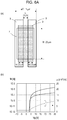
- FIGS. 6A (a) and 6 A(b) are a plan view of a TFT of Comparative Example 1 and a graph illustrating Vg-Id characteristics of the TFT of Comparative Example 1, respectively.
- FIGS. 6B (a) and 6 B(b) are a plan view of the TFT of Example 1 and a graph illustrating Vg-Id characteristics of the TFT of Example 1, respectively.
- FIGS. 7( a ) and 7( b ) are a plan view of a TFT of Comparative Example 2 and a plan view of a TFT of Example 2, respectively, and FIG. 7( c ) is a graph illustrating a relationship between an offset width Loff and an on current ratio in the TFTs of Comparative Example 2 and Example 2.
- FIGS. 8( a ) and 8( b ) are plan views that illustrate circuit TFTs (thin-film transistor 30 D, 30 E) in a second embodiment, respectively.
- FIGS. 9( a ) and 9( b ) are a plan view and a cross-sectional view that illustrate a circuit TFT (thin-film transistor 30 F) of a third embodiment, respectively.
- FIGS. 10( a ) and 10( b ) are a plan view and a cross-sectional view that illustrate another circuit TFT (thin-film transistor 30 G) of the third embodiment, respectively, and FIG. 10( c ) is a plan view of the thin-film transistor 30 G when misalignment occurs.
- FIGS. 11( a ) and 11( b ) are plan views that illustrate still another circuit TFTs (thin-film transistors 30 H, 30 I) of the third embodiment, respectively.
- FIG. 12 is a diagram for describing a configuration and an operation of an SSD circuit 100 in an active matrix substrate 1000 .
- FIG. 13 is a plan view illustrating an SSD unit circuit 110 .
- FIGS. 14( a ) and 14( b ) are a plan view of a pixel area P in the active matrix substrate 1000 , and a cross-sectional view taken along line IV-IV, respectively.
- FIG. 15 is a plan view illustrating a thin-film transistor 300 of Reference Example.
- an active matrix substrate according to a first embodiment will be described below with reference to the drawings.
- an active matrix substrate in which an SSD circuit and a gate driver are monolithically formed and a source driver is mounted will be described below.
- a peripheral circuit including at least one TFT may be monolithically formed.
- FIG. 1 is a schematic diagram illustrating an example of a planar structure of an active matrix substrate 1000 according to the present embodiment.
- the active matrix substrate 1000 has a display area DR and an area (a non-display area or a frame area) FR other than the display area DR.
- the display area DR is configured with pixel areas P that are arranged in a matrix form.
- the pixel area P (also referred to simply as “pixel” in some cases) is an area that corresponds to a pixel of a display device.
- the non-display area FR is an area that is positioned in the vicinity of the display area DR and does not contribute to display.
- the non-display area FR includes a terminal-portion formation area in which a terminal portion is formed, a drive circuit formation area in which a drive circuit is integrally (monolithically) formed, and the like.
- a gate driver GD, an SSD circuit 100 , and the like are monolithically provided in the drive circuit formation area.
- a source driver SD for example, is mounted in the active matrix substrate 1000 .
- the gate driver GD is positioned in an area FRa that is positioned on both the sides of the display area DR
- the source driver SD is mounted in an area FRb that is positioned under the display area DR.
- the SSD circuit 100 is positioned between the display area DR and the source driver SD in the area FRb.
- Each pixel area P is defined by the gate bus line GL and the source bus line SL.
- Each of the gate bus lines GL is connected to a corresponding terminal of the gate driver GD.
- Each of the source bus lines SL is connected to a corresponding terminal of the source driver SD.
- Each pixel area P has a TFT (hereinafter, referred to as “pixel TFT”) 10 and a pixel electrode PE.
- a gate electrode of the pixel TFT 10 is electrically connected to the corresponding gate bus line GL, a source electrode thereof is electrically connected to the corresponding source bus line SL.
- a drain electrode is electrically connected to the pixel electrode PE.
- an electrode a common electrode that is common to multiple pixels is provided in the active matrix substrate 1000 .
- FIGS. 2A (a) and 2 A(b) are a plan view and a cross-sectional view, respectively, that illustrate a circuit TFT (thin film transistor 30 A) included in peripheral circuits that are monolithically formed in the active matrix substrate 1000 according to the present embodiment.
- the thin-film transistor 30 A can be used as a switching element of the SSD circuit.
- the active matrix substrate 1000 according to the present embodiment may have at least one TFT transistor 30 A as the circuit TFT and may further have a circuit TFT having a different structure.
- the thin-film transistor 30 A is supported on the substrate 1 and is formed in a non-display area.
- the thin-film transistor 30 A includes a gate electrode 3 (also referred to as “first gate electrode”) disposed on the substrate 1 , a gate insulation layer 5 covering the gate electrode 3 , an oxide semiconductor layer 7 , a source electrode 8 , and a drain electrode 9 .
- the oxide semiconductor layer 7 is disposed on the gate insulation layer 5 so as to at least partially overlap with the gate electrode 3 via the gate insulation layer 5 .
- the source electrode 8 is provided on the oxide semiconductor layer 7 and is in contact with an end p 1 of the oxide semiconductor layer 7 .
- the drain electrode 9 is provided on the oxide semiconductor layer 7 and is in contact with an end portion p 2 (end portion facing the end p 1 ) of the oxide semiconductor layer 7 .
- a portion in contact with the source electrode 8 is referred to as a source contact area 7 s
- a portion in contact with the drain electrode 9 is referred to as a drain contact area 7 d .
- the source contact area 7 s is disposed at the end portion p 1 of the oxide semiconductor layer 7
- the drain contact area 7 d is disposed at the other end portion p 2 positioned on the opposite side across a channel region 7 c .
- a region positioned between the source contact area 7 s and the drain contact area 7 d and overlaps with the gate electrode 3 is “channel region 7 c”.
- a direction DL parallel to the direction in which current flows in the channel region 7 c is referred to as “channel length direction”, and a direction DW orthogonal to the channel length direction DL is referred to as “channel width direction”.
- the length in the channel length direction DL in the channel region 7 c is the channel length L
- the length in the channel width direction DW is the channel width W.
- the channel length direction DL is a direction connecting end portions p 1 and p 2 . From the end portion p 1 to the end portion p 2 , the source contact area 7 s , the channel region 7 c and the drain contact area 7 d are arranged in this order in the channel length direction DL.
- the channel length direction DL a direction in which end portions p 1 and p 2 of the oxide semiconductor layer 7 are connected or a direction in which the source contact area 7 s and the drain contact area 7 d are connected with the shortest distance therebetween.
- the source electrode 8 and the drain electrode 9 may be designed to overlap with the gate electrode 3 when viewed in the direction normal to the substrate 1 .
- the lengths xs and xd of the portions where the source electrode 8 and the drain electrode 9 overlap with the gate electrode 3 can be set in consideration of alignment accuracy.
- the gate electrode 3 has a first edge portion 3 e 1 and a second edge portion 3 e 2 , which face each other, when viewed in the direction normal to the substrate 1 .
- the first edge portion 3 e 1 and the second edge portion 3 e 2 generally extend across the oxide semiconductor layer 7 in the channel width direction DW.
- the first edge portion 3 e 1 crosses one end p 1 of the oxide semiconductor layer 7
- the second edge portion 3 e 2 crosses the other end p 2 of the oxide semiconductor layer 7 .
- the width wg of the gate electrode 3 in the channel length direction DL is smaller than the width ws of the oxide semiconductor layer 7 in the channel length direction DL.
- the second edge portion 3 e 2 has a recess portion 40 (also referred to as “first recess portion” in some cases) in a region overlapping with the oxide semiconductor layer 7 .
- the recess portion 40 is a portion where the edge portion of the gate electrode 3 is recessed in the channel length direction DL in the plane parallel to the substrate 1 .
- the planar shape of the recess portion 40 is not limited to a rectangular shape as shown. Depending on a method of patterning the gate electrode 3 , the recess portion 40 may have a rounded planar shape such as a U-shape.
- first part a portion 41 of the gate electrode 3 , which overlaps with the oxide semiconductor layer 7 and is adjacent to the recess portion 40 in the channel width direction DW (in this example, parts positioned on both sides of the recess portion 40 ), is referred to as “first part”.
- the source electrode 8 or the drain electrode 9 (here, the drain electrode 9 ) is arranged so as to overlaps with at least part of the recess portion 40 or at least part of the first part 41 of the gate electrode 3 when viewed in the direction normal to the substrate 1 .
- the source electrode 8 or the drain electrode 9 is designed to overlap with the first part 41 of the gate electrode 3 by the predetermined lengths xs and xd, a predetermined on current can be secured even when misalignment occurs in any direction in the channel length direction DL.
- the source electrode 8 or the drain electrode 9 overlaps with at least part of the recess portion 40 of the gate electrode 3 , the gate-source/drain parasitic capacitance can be reduced.
- the second edge portion 3 e 2 has the recess portion 40 , and the drain electrode 9 is disposed to overlap with at least part of the recess portion 40 (preferably, the whole recess portion 40 ).
- the overlap area of the drain electrode 9 and the gate electrode 3 can be reduced, the gate-drain capacitance Cgd can be reduced.
- the source electrode 8 and the drain electrode 9 is formed using the same conductive layer as the source bus line SL ( FIG. 1 ).
- the layer formed using the same conductive layer as the source bus line SL is referred to as “source metal layer”.
- the gate electrode 3 is formed using the same conductive layer as the gate bus line GL ( FIG. 1 ).
- the layer formed using the same conductive layer as the gate bus line GL is referred to as “gate metal layer”.
- the thin-film transistor 30 A is covered with a protective layer 11 (here, an inorganic insulation layer).
- the inorganic insulation layer 11 is disposed to be in contact with the upper surfaces of the source electrode 8 and the drain electrode 9 and with the channel region 7 c of the oxide semiconductor layer 7 .
- FIG. 15 is a plan view illustrating a thin-film transistor 300 of Reference Example.
- TFT width the width of the TFT in the channel length direction DL
- W the width of the oxide semiconductor layer 7
- the circuit TFT allowing a relatively large current to flow can be used.
- Japanese Unexamined Patent Application Publication No. 64-84297 discloses that a TFT having such a configuration is used for a demultiplexer of a display device.
- the gate-source parasitic capacitance Cgs is formed in the portion where the source electrode 8 and the gate electrode 3 overlap with each other, and the gate-drain parasitic capacitance Cgd is formed in the portion where the drain electrode 9 and the gate electrode 3 overlap with each other.
- the lengths xs, xd (overlap lengths) of the portion where the source electrode 8 and the drain electrode 9 overlaps with the gate electrode 3 can be set in consideration of alignment accuracy.
- the region (offset region) which does not overlap with any of the gate electrode 3 , the source electrode 8 , and the drain electrode 9 can be set so as not to be formed in the oxide semiconductor layer 7 .
- the thin-film transistor 300 is further enhanced in definition (that is, the channel length L is further shortened)
- the ratio of the overlap lengths xs and xd to the channel length L increases, and the parasitic capacitances Cgs and Cgd also increase the influence on the TFT characteristics.
- the thin-film transistor 30 A ( FIG. 2A ) according to the present embodiment has the recess portion 40 that is recessed in the channel length direction DL in the first edge portion 3 e 1 or the second edge portion 3 e 2 of the gate electrode 3 .
- a part or the whole of the recess portion 40 overlaps with the source electrode 8 or the drain electrode 9 .
- the overlap area of the gate electrode 3 and the source electrode 8 or the drain electrode 9 is smaller than that of the thin-film transistor 300 by the area of the portion where the recess portion 40 overlaps with the source electrode 8 or the drain electrode 9 , and as a result, the gate-source/drain parasitic capacitances Cgd, Cgs can be reduced.
- the lengths xs and xd of the portion where the source electrode 8 and the drain electrode 9 overlap with the gate electrode 3 (or a first part 41 of the gate electrode 3 ) can be set in consideration of alignment accuracy similarly to the thin-film transistor 300 . Therefore, the TFT width wT is the same between the thin-film transistor 30 A and the thin-film transistor 300 .
- the present embodiment it is possible to reduce the TFT width wT to the same level as that of the thin-film transistor 300 while suppressing the parasitic capacitances (sum of Cgs and Cgd) smaller than that of the thin-film transistor 300 .
- the present embodiment even when misalignment occurs, a predetermined on current can be secured. Therefore, it is possible to reduce the parasitic capacitances Cgd and Cgs while maintaining high reliability.
- the source electrode 8 or the drain electrode 9 partially overlaps with the recess portion 40 when viewed in the direction normal to the substrate 1 . In this case, an offset region 7 off is likely to be present on the oxide semiconductor layer 7 .
- the offset region Toff refers to the area that, when viewed in the direction normal to the substrate 1 , is positioned between the channel region 7 c and the source electrode 8 and the drain electrode 9 in the oxide semiconductor layer 7 and that does not overlap with any of the source electrode 8 , the drain electrode 9 and the gate electrode 3 .
- the width Loff of the offset region Toff in the channel length direction DL is referred to as “offset width”.
- the offset width Loff is equal to or shorter than lengths xd and xs. In general, when the offset region is generated, the offset region has a higher resistance than the channel region in the on state of the TFT. In this way, the on current of the TFT may be reduced.
- the region 7 n adjacent to the offset region Toff in the channel width direction DW in the oxide semiconductor layer 7 overlaps with the first part 41 of the gate electrode 3 and can function as the channel region 7 c .
- the offset region Toff is not formed across the channel region 7 c and the source contact area 7 s or the drain contact area 7 d in the oxide semiconductor layer 7 , it is possible to suppress reduction in the on current caused by the offset region 7 off.
- the width f 1 (the maximum width) of the recess portion 40 may be, for example, 20% or more, preferably 30% or more, of the channel width W of the oxide semiconductor layer 7 . This can more effectively reduce the gate-source/drain overlap area.
- the width f 1 may be 80% or less, preferably 50% or less, of the channel width W of the oxide semiconductor layer 7 . Even when the offset region Toff is present due to misalignment, it is possible to effectively suppress reduction in the on current caused by the offset region 7 off.
- the depth h 1 (the maximum step value) of the recess portion 40 in the channel length direction can be preferably set to be less than the overlap lengths xs and sd of the gate electrode 3 and the source electrode 8 or the drain electrode 9 in the channel length direction DL. Therefore, the offset region Toff is less likely to be present, and if present, the region can be formed to be smaller.
- the lengths xs and xd differ depending on a manufacturing device and the like and are, for example, 1.5 ⁇ m or more and 3.0 ⁇ m or less.
- the depth h 1 of the recess portion 40 may be equal to or less than, preferably 80% or less of, the channel length L of the oxide semiconductor layer 7 (the minimum value of the distance between the source contact area 7 s and the drain contact area 7 d ). This makes it possible to suppress the parasitic capacitance to a small amount while securing the on current. Meanwhile, the length h 1 may be 20% or more, preferably 50% or more, of the channel length L of the oxide semiconductor layer 7 . This makes it possible to more effectively reduce the gate-source/drain overlap area.
- the thin-film transistor 30 A may be a circuit TFT that allows a relatively large current to flow, such as a switching TFT (hereinafter, referred to as an SSD circuit TFT) that is a part of the SSD circuit, and the like.
- a switching TFT hereinafter, referred to as an SSD circuit TFT
- the width of the circuit TFT (TFT width) in the channel length direction can be reduced while securing the on current by increasing the channel width W of the circuit TFT, and therefore, narrowing of the frame can be implemented.
- the present embodiment is applied to the high definition active matrix substrate having a narrow arrangement pitch of the source bus lines SL (for example, 10 ⁇ m or less), it is possible to advantageously dispose the SSD circuit TFT between source bus lines SL adjacent to each other.
- the structure of the thin-film transistor 30 A is not limited to the example shown in FIG. 2A .
- the recess portion 40 may be provided only to the first edge portion 3 e 1 of the gate electrode 3 .
- the overlap area of the drain electrode 9 and the gate electrode 3 it is preferable to design the overlap area of the drain electrode 9 and the gate electrode 3 to be smaller than the overlap area of the source electrode 8 and the gate electrode 3 .
- the recess portion 40 when the recess portion 40 is provided to only one of the first edge portion 3 e 1 and the second edge portion 3 e 2 of the gate electrode 3 , it is preferable to provide the recess portion 40 to the second edge portion 3 e 2 that is positioned on the drain side.
- the gate electrode 3 may have the recess portion 40 in both edge portions 3 e 1 and 3 e 2 when viewed in the direction normal to the substrate 1 .
- two or more recess portions 40 may be arranged at intervals.
- one edge portion may have a recess portion, and the other edge portion may have a protruding portion.
- the recess portion 40 and the protruding portion of the gate electrode 3 are not limited to a rectangular shape and may have a rounded shape.
- the planar shapes of the source electrode 8 and the drain electrode 9 are not particularly limited. However, it is preferable that the source electrode 8 and the drain electrode 9 not have a comb structure (see PTL 1). When the structure has a comb shape, the size and the parasitic capacitance of the TFT are increased.
- FIG. 3( a ) is a plan view illustrating another circuit TFT (a thin film transistor 30 B) according to the present embodiment
- FIG. 3( b ) is a plan view of the thin film transistor 30 B when misalignment occurs.
- the thin-film transistor 30 B is different from the thin-film transistor 30 A in that, when viewed in the direction normal to the substrate 1 , both the first edge portion 3 e 1 and the second edge portion 3 e 2 of the gate electrode 3 have recess portions 40 s and 40 d (collectively referred to as “recess portion 40 ” in some cases) in the region overlapping with the oxide semiconductor layer 7 .
- the source electrode 8 and the drain electrode 9 overlap with at least part of the corresponding recess portions 40 . In the illustrated example, the source electrode 8 and the drain electrode 9 overlap with the entire corresponding recess portions 40 .
- the gate-drain parasitic capacitance Cgd of the thin-film transistor 30 B can be reduced. Therefore, it is possible to reduce the width wT of the thin-film transistor 30 B in the channel length direction DL while suppressing the influence of the parasitic capacitance more effectively.
- the region 7 n adjacent to the offset region Toff in the channel length direction DL overlaps with the first part 41 of the gate electrode 3 and can function as the channel region 7 c . Therefore, a predetermined on current can be secured.
- FIG. 4( a ) is a plan view illustrating still another circuit TFT (a thin film transistor 30 C) according to the present embodiment
- FIG. 4( b ) and FIG. 4( c ) are plan views of the thin film transistor 30 C when respective misalignments occur.
- the first edge portion 3 e 1 and the second edge portion 3 e 2 of the gate electrode 3 when viewed in the direction normal to the substrate 1 , one of the first edge portion 3 e 1 and the second edge portion 3 e 2 of the gate electrode 3 (here, the second edge portion 3 e 2 ) has the recess portion 40 in the region overlapping with the oxide semiconductor layer 7 , and the other end (here, the first edge portion 3 e 1 ) has a protruding portion 42 (also referred to as a first protruding portion) in the region overlapping with the oxide semiconductor layer 7 .
- the protruding portion 42 indicates the portion where the edge portion of the gate electrode 3 protrudes in the channel length direction DL in the plain parallel to the substrate 1 .
- the edge portion of the gate electrode 3 has two notch portions 43 at an interval, and the portion between the notch portions 43 is the protruding portion 42 .
- one (here, the drain electrode 9 ) of the source electrode 8 and the drain electrode 9 overlaps with at least a part of the recess portion 40 and at least a part of the first part 41
- the other (here, the source electrode 8 ) overlaps with at least a part of the protruding portion 42 and at least a part of the notch portions 43 .
- the source electrode 8 and the drain electrode 9 may overlap with the entire protruding portion 42 or the entire recess portion 40 .
- the overlap area of the gate electrode 3 and the drain electrode 9 can be reduced by the overlap area of the drain electrode 9 and the recess portion 40 of the gate electrode 3 , and as a result, the gate-drain parasitic capacitance Cgd can be reduced. Furthermore, since the overlap area of the gate electrode 3 and the source electrode 8 can be reduced by the overlap area of the source electrode 8 and the notch portions 43 of the gate electrode 3 , it is also possible to reduce the gate-source parasitic capacitance Cgs.
- the height h 2 and the width f 2 of the protruding portion 42 of the gate electrode 3 can be set in the same range as the width f 1 and the h 1 of the recess portion 40 , respectively.
- the length xs of the portion where the source electrode 8 overlaps with the protruding portion 42 of the gate electrode 3 , and the length xd of the portion where the drain electrode 9 and the first part 41 of the gate electrode 3 can be set in consideration of the alignment accuracy. Even when misalignment occurs in any direction in the channel length direction DL, the offset region is not present over the entire channel width W, and as a result, a predetermined on current can be secured.
- the oxide semiconductor layer 7 may overlap with the notch portion 43 of the gate electrode 3 , and the overlapped portion may be the offset region 7 off.
- the region 7 n positioned between two offset regions Toff overlaps with the protruding portion 42 of the gate electrode 3 , and can function as the channel region 7 c . Therefore, since the offset region Toff is not present across the source contact area 7 s and the channel region 7 c , it is possible to suppress reduction in the on current.
- a part of the oxide semiconductor layer 7 may overlap with the recess portion 40 of the gate electrode 3 , and the overlapped portion may be the offset region 7 off.
- the region 7 n positioned on both sides of the offset region Toff overlaps with the first part 41 of the gate electrode 3 , and can function as the channel region 7 c . Therefore, since the offset region Toff is not present across the drain contact area 7 d and the channel region 7 c , it is possible to suppress reduction in the on current.
- the TFT width wT can be reduced to the same extent as the thin-film transistors 30 A, 30 B.
- the width wg of the gate electrode 3 of the thin-film transistor 30 C in the channel length direction DL is, for example, L+xd (or L+xs), and is smaller than the width wg (L+xd+xs) of the thin-film transistors 30 A and 30 B.
- the structure of the circuit TFT is not limited to that described above.
- the sizes of the recess portion 40 and the protruding portion 42 of the gate electrode 3 may be set such that, when viewed in the direction normal to the substrate 1 , the overlap area of the drain electrode 9 and the gate electrode 3 is smaller than the overlap area the source electrode 8 and the gate electrode 3 .
- the width of the recess portion 40 d of the gate electrode 3 may be larger than the width of the recess portion 40 s . This makes it possible to further reduce the gate-drain capacitance Cgd.
- the recess portion 40 or the protruding portion 42 of the gate electrode 4 is disposed in the vicinity of the center of the channel width W, but the recess portion 40 or the protruding portion 42 may be disposed at a position shifted from the center.
- the thin-film transistors 30 A to 30 C may be designed such that the oxide semiconductor layer 7 has the offset region Toff equal to or less than a predetermined width (for example, the offset width Loff of 2 ⁇ m or less) in a region positioned on the recess portion 40 (or notch portion 43 ) of the gate electrode 3 .
- FIG. 5 is a plan view illustrating a TFT structure in which the offset region Toff is intentionally provided in the thin-film transistor 30 B. As described above, the intentional formation of the offset region Toff makes it possible to further reduce the parasitic capacitance while maintaining a predetermined off current.
- the inventors manufactured a TFT of Comparative Example 1 in which the recess portion was not provided in the gate electrode 3 and a TFT of Example 1 in which the recess portion 40 was provided in the gate electrode 3 , and measured Vg-Id characteristics. Hereinafter, the result will be described.
- FIGS. 6A (a) and 6 A(b) are a plan view of a TFT of Comparative Example 1 and a graph illustrating Vg-Id characteristics of the TFT of Comparative Example 1, respectively.
- FIGS. 6B (a) and 6 B(b) are a plan view of the TFT of Example 1 and a graph illustrating Vg-Id characteristics of the TFT of Example 1, respectively.
- the TFT of Comparative Example 1 has the configuration similar to the thin-film transistor 300 described above with reference to FIG. 15 .
- the TFT of Example 1 has recess portions 40 at both the first edge portion 3 e 1 and the second edge portion 3 e 2 of the gate electrode 3 (which is similar to the thin-film transistor 30 B described above with reference to FIG. 4 ).
- Channel lengths L, channel widths W, overlap lengths xs and xd of the gate electrode 3 and the source electrode 8 and the drain electrode 9 , and the TFT widths wT of the TFT of Example 1 and the TFT of Comparative Example 1, and the size (width f 1 and depth h 1 ) of the recess portion 40 of the TFT of Example 1 are illustrated in FIGS. 6A (a) and 6 B(a).
- the size of the recess portion 40 was set such that the overlap area of the source/drain electrode in the TFT of Example 1 and the gate electrode was approximately 50% of the overlap area of the TFT of Comparative Example 1.
- Vg-Id characteristics were performed at room temperature using a semi-automatic prober (4156C) device.
- the gate scan voltage Vg was ⁇ 10 V to +30 V
- the drain voltage Vd was 0.1 V and 20 V.
- the field effect mobility ⁇ was calculated from the measurement results of the Vg-Id characteristics of each TFT.
- FIGS. 7( a ) and 7( b ) are a plan view of a TFT of Comparative Example 2 and a plan view of a TFT of Example 2, respectively.
- the TFTs of Comparative Example 2 and Example 2 are different from the TFTs ( FIGS. 6A and 6B ) of Comparative Example 1 and Example 1, respectively, in that the offset regions Toff are formed on the source side and the drain side of the oxide semiconductor layer 7 .
- the offset regions Toff are formed on both the source side and the drain side of the oxide semiconductor layer 7
- the offset region Toff may be present on only one of the source side and the drain side when the offset region Toff is present due to misalignment.
- a relationship between the offset width Loff and the on current ratio was calculated when the width Loff of the offset region Toff (offset width) is made different by moving the source electrodes 8 and the drain electrodes 9 of the TFTs of Comparative Example 2 and Example 2 in a direction away from the channel region 7 c .
- the result was shown in FIG. 7( c ) .
- the horizontal axis represents the offset width Loff, and when the source electrode 8 and the drain electrode 9 overlaps with the gate electrode 3 , Loff is expressed as positive, and when the source electrode 8 and the drain electrode 9 overlaps with the gate electrode 3 , Loff is expressed as negative.
- the “on current ratio” on the vertical axis is the ratio to the on current when the offset width Loff is zero.
- the on current ratio is approximately 80% or more when the offset width Loff is less than 2 ⁇ m, and approximately 90% or more when the offset width Loff is 1 ⁇ m or less. Therefore, it is confirmed that, when the offset width Loff is set to be smaller than a predetermined width in consideration of alignment accuracy, predetermined TFT characteristics can be secured.
- the circuit TFT in the second embodiment is different from the circuit TFT in the first embodiment in that the source electrode or the drain electrode has a recess portion or a protruding portion when viewed in the direction normal to the substrate.
- FIGS. 8( a ) and 8( b ) are plan views that illustrate circuit TFTs (thin-film transistor 30 D, 30 E) in the second embodiment, respectively.
- the same components as those in FIGS. 2A to 4 are denoted by the same reference signs.
- Source electrodes 8 of the thin-film transistors 30 D and 30 E have edge portions 8 e (hereinafter, referred to as “source edge portions”) that opposes drain electrodes 9 .
- the drain electrodes 9 have edge portions 9 e (hereinafter, referred to as “drain edge portions”) that opposes the source electrodes 8 .
- the source edge portion 8 e and/or the drain edge portion 9 e has a protruding portion 52 (also referred to as “second protruding portion”) protruding in the channel length direction DL or a recess portion 50 (also referred to as “second recess portion”) recessed in the channel length direction DL, in a region overlapping with the oxide semiconductor layer 7 .
- the recess portion 50 or the protruding portion 52 is disposed to overlap with the recess portion 40 of the gate electrode 3 .
- the thin-film transistor 30 D illustrated in FIG. 8( a ) is different from the thin-film transistor 30 B in that the source edge portion 8 e of the source electrode 8 has a recess portion 50 s and the drain edge portion 9 e of the drain electrode 9 has a recess portion 50 d when viewed in the direction normal to the substrate 1 .
- the recess portions 50 s and 50 d (collectively referred to as “recess portion 50 ” in some cases) of the source electrode 8 and the drain electrode 9 overlap with at least parts of the recess portions 40 s and 40 d (collectively referred to as “recess portion 40 ” in some cases) of the gate electrode 3 , respectively.
- an overlap portion of the recess portion 50 s of the source electrode 8 and the recess portion 40 s of the gate electrode 3 , and an overlap portion of the recess portion 50 d of the drain electrode 9 and the recess portion 40 d of the gate electrode 3 are offset regions Toff, respectively.
- the overlap region of the gate electrode 3 and the source electrode 8 and the drain electrode 9 can be made smaller than the thin-film transistor 30 B, which, in turn, makes it possible to further reduce parasitic capacitances Cgd and Cgs between the source/drain electrode and the gate electrode.
- the offset region Toff it is possible to make the TFT width wT smaller than the example illustrated in FIG. 5 .
- increase in the overlap area of the gate electrode 3 and the source electrode 8 and the drain electrode 9 is suppressed more than the thin-film transistor 30 B.
- the depth h 1 of the recess portion 40 of the gate electrode 3 and the depth h 3 of the recess portion 50 of the source electrode 8 and the drain electrode 9 may be set such that the width Loff of the offset region Toff is, for example, 2 ⁇ m or less. This makes it possible to more reliably suppress reduction in the on current caused by the offset region 7 off.
- the depth h 3 of the recess portion 50 may be smaller than the depth h 1 of the recess portion 40 .
- the width f 3 of the recess portion 50 of the source electrode 8 and the drain electrode 9 may be set within the same range as the width f 1 of the recess portion 40 of the gate electrode 3 .
- the width f 3 of the recess portion 50 of the source electrode 8 and the drain electrode 9 may be smaller than the width f 1 of the recess portion 40 of the gate electrode 3 .
- the side wall portion of the recess portions 50 of the source electrode 8 and the drain electrode 9 are disposed on the channel region 7 c . This allows current not only to flow linearly as indicated by arrow 81 , but also to flow curvilinearly by the side wall portions of the recess portions 50 s and 50 d as indicated by arrow 82 . As a result, reduction in the on current caused by the offset region Toff can be more effectively suppressed.
- the recess portion 50 is provided in both the source electrode 8 and the drain electrode 9 , but may be provided at only one of them.
- the gate electrode 3 may have the recess portion 40 below the source electrode 8 or the drain electrode 9 , and may have the recess portion 40 at only one of the first edge portion 3 e 1 and the second edge portion 3 e 2 .
- the gate electrode 3 has the protruding portion 42 at one of the first edge portion 3 e 1 and the second edge portion 3 e 2 , and the recess portion 40 at the other of the first edge portion 3 e 1 and the second edge portion 3 e 2 , in the region overlapping with the oxide semiconductor layer 7 , when viewed in the direction normal to the substrate 1 .
- one (here, the drain edge portion 9 e ) of the source edge portion 8 e of the source electrode 8 and the drain edge portion 9 e of the drain electrode 9 has the protruding portion 52
- the other (here, source edge portion 8 e ) has the recess portion 50 .
- the drain edge portion 9 e has two notch portions 53 disposed at an interval, and the portion positioned between the notch portions 53 is the protruding portion 52 .
- the protruding portion 52 of the drain electrode 9 overlaps with at least a part of the recess portion 40 of the gate electrode 3
- the recess portion 50 of the source electrode 8 overlaps with at least a part of the protruding portion 42 of the gate electrode 3 .
- the overlap portion of the recess portion 50 of the source electrode 8 and the recess portion 40 of the gate electrode 3 , and the overlap portion of the notch portion 53 of the drain electrode 9 and the notch portion 43 of the gate electrode 3 are offset regions Toff, respectively.
- the overlap area of the gate electrode 3 and the source electrode 8 and the drain electrode 9 can be made smaller than that of the thin-film transistor 30 C, it is possible to reduce the parasitic capacitances Cgd, Cgs between the source/drain electrodes and the gate electrode.
- misalignment occurs in the channel length direction DL, increase in the overlap area of the gate electrode 3 and the source electrode 8 or the drain electrode 9 is suppressed more than the thin-film transistor 30 C.
- the depth h 1 of the recess portion 40 and the height h 2 of the protruding portion 42 , of the gate electrode 3 , and the depth h 3 of the recess portion 50 and the height h 4 of the protruding portion 52 , of the source electrode 8 or the drain electrode 9 may be set such that the width Loff of the offset region Toff is, for example, less than 2 ⁇ m. This makes it possible to more reliably suppress reduction in the on current caused by the offset region 7 off.
- the depth h 3 of the recess portion 50 may be smaller than the depth h 1 of the recess portion 40 .
- the height h 4 of the protruding portion 52 may be smaller than the height h 2 of the protruding portion 42 .
- the widths f 3 and f 4 of the recess portion 50 and the protruding portion 52 of the source electrode 8 or the drain electrode 9 may be set within the same range as the widths f 1 and f 2 of the recess portion 40 and the protruding portion 42 of the gate electrode 3 .
- the widths f 3 and f 4 of the recess portion 50 and the protruding portion 52 of the source electrode 8 and the drain electrode 9 may be smaller than the widths f 1 and f 2 of the recess portion 40 and the protruding portion 42 of the gate electrode 3 .
- the side wall portions of the recess portion 50 and the protruding portion 52 of the source electrode 8 and the drain electrode 9 are disposed on the channel region 7 c . This allows current not only to flow linearly as indicated by arrow 83 , but also to flow curvilinearly by the side wall portions of the recess portion 50 and the protruding portion 52 as indicated by arrow 84 . As a result, reduction in the on current caused by the offset region Toff can be more effectively suppressed.
- the protruding portion 42 may be provided at the first edge portion 3 e 1 and the recess portion 40 may be provided at the second edge portion 3 e 2 .
- the protruding portion 52 may be provided at the source electrode 8 and the recess portion 50 may be provided at the drain electrode 9 .
- circuit TFT on an active matrix substrate of a third embodiment will be described.
- differences from the first embodiment will be mainly described, and description of the same configuration as that of the first embodiment will be omitted.
- the circuit TFT in the third embodiment is different from the circuit TFT in the first embodiment in that it has gate electrodes on the side of the substrate 1 of the oxide semiconductor layer 7 and on the side opposite to the substrate 1 , respectively (double gate configuration).
- FIGS. 9( a ) and 9( b ) are a plan view and a cross-sectional view that illustrate the circuit TFT (thin-film transistor 30 F) of the present embodiment, respectively.
- the thin-film transistor 30 F also has another gate electrode 23 (hereinafter, referred to as “upper gate electrode”, and in some cases, referred to as “second gate electrode”) above the oxide semiconductor layer 7 , that is, on the side opposite to the substrate 1 of the oxide semiconductor layer 7 .
- Other structures are similar to, for example, the thin-film transistor 30 B illustrated in FIG. 3 .
- the upper gate electrode 23 is disposed on the oxide semiconductor layer 7 via an insulation film. When viewed in the direction normal to the substrate 1 , the upper gate electrode 23 at least partially overlaps with the oxide semiconductor layer 7 .
- the thin-film transistor 30 F is covered with the inorganic insulation layer 11 (passivation layer), and the upper gate electrode 23 is disposed on the inorganic insulation layer 11 . That is, the inorganic insulation layer 11 also serves as a gate insulation film of the upper gate electrode 23 .
- the gate insulation film positioned between the oxide semiconductor layer 7 and the gate electrode 3 and the gate insulation film positioned between the oxide semiconductor layer 7 and the upper gate electrode 23 are distinguished by being referred to as “first gate insulation film” and “second gate insulation film”, respectively.
- the upper gate electrode 23 is disposed to partially overlap with the source electrode 8 and the drain electrode 9 when viewed in the direction normal to the substrate 1 .
- the length of the overlap portion in the channel length direction DL may be the same as the overlap lengths xd and xs of the gate electrode 3 and the source electrode 8 and the drain electrode 9 .
- the upper gate electrode 23 may be, for example, a transparent electrode formed using the same transparent conductive layer as the transparent electrode (for example, pixel electrode) disposed in the display area.
- a lower transparent electrode and an upper transparent electrode are disposed on the display area via a dielectric layer.
- One of the lower transparent electrode and the upper transparent electrode is a pixel electrode, and the other is a common electrode.
- the upper gate electrode 23 can be formed using the same transparent conductive film as the lower transparent electrode or the upper transparent electrode.
- the inorganic insulation layer 11 which is a passivation film can function as a second gate insulation film.
- the inorganic insulation layer 11 and the dielectric layer 17 can function as a second gate insulation film.
- the upper gate electrode 23 has the same planar shape as the gate electrode 3 . That is, the upper gate electrode 23 may have recess portions (also referred to as “third recess portions”) 60 s and 60 d (collectively referred to as “recess portion 60 ” in some cases) at positions corresponding to the recess portions 40 s and 40 d (collectively referred to as “recess portion 40 ” in some cases) of the gate electrode 3 .
- the upper gate electrode 23 has an edge portion 23 e 1 (also referred to as “third edge portion”) and an edge portion 23 e 2 (also referred to as “fourth edge portion”) that oppose each other, and the edge portions 23 e 1 and 23 e 2 extend across the oxide semiconductor layer 7 in the channel width direction DW.
- the edge portions 23 e 1 and 23 e 2 have recess portions 60 s and 60 d recessed in the channel length direction DL, and a second part 61 adjacent to the recess portions 60 s and 60 d in the channel width direction DW, in the region overlapping with the oxide semiconductor layer 7 .
- the recess portion 60 s and the recess portion 40 s at least partially overlap with each other, and the recess portion 60 d and the recess portion 40 d at least partially overlap with each other.
- the source electrode 8 and the drain electrode 9 at least partially overlap with the recess portion 40 and the first part 41 of the gate electrode 3 , and at least partially overlap with the recess portion 60 and the second part 61 of the gate electrode 23 , respectively. Since the overlap area of the upper gate electrode 23 and the source electrode 8 and the drain electrode 9 is reduced by the overlap area of the recess portion 60 of the upper gate electrode 23 and the source electrode 8 and the drain electrode 9 , it is possible to suppress the parasitic capacitances to be smaller than the case where the recess portion is not formed at the upper gate electrode 23 .
- the thin-film transistor 30 F can increase the on current more than the TFT having a single gate structure, and can implement higher electric current drive force. Further, according to the present embodiment, the parasitic capacitance between the gate electrode 3 and the source electrode 8 and the drain electrode 9 and the parasitic capacitance between the upper gate electrode 23 and the source electrode 8 and the drain electrode 9 are reduced, and thus the size (width wT in the channel length direction DL) of the thin film transistor 30 F can be reduced. Further, even when misalignment occurs, a predetermined on current can be secured, such that the parasitic capacitance can be reduced while maintaining high reliability.
- the width f 5 and the depth h 5 of the recess portion 60 of the upper gate electrode 23 can be set within the same range as the width f 1 and the depth h 1 of the recess portion 40 of the gate electrode 3 , respectively.
- the width f 5 may be the same as the width f 1 or may be smaller than the width f 1 . This makes it possible more effectively suppress increase in parasitic capacitance.
- the depth h 5 may be the same as the depth h 1 of the recess portion 40 of the gate electrode 3 or may be smaller than the depth h 1 .
- the recess portion 60 and the recess portion 40 may be designed to be substantially aligned.
- the recess portion 60 is provided to both of the two edge portions 23 e 1 and 23 e 2 of the upper gate electrode 23 , but may be provided to only one of them.
- the gate electrode 3 may have the recess portion 40 at least below the recess portion of the upper gate electrode 23 , and may have the recess portion 40 only at one of the first edge portion 3 e 1 and the second edge portion 3 e 2 .
- FIGS. 10( a ) and 10( b ) are a plan view and a cross-sectional view that illustrate another circuit TFT (thin-film transistor 30 G) of the third embodiment, respectively.
- the thin-film transistor 30 G is different from the thin-film transistor 30 F illustrated in FIG. 9 in that the upper gate electrode 23 has a planar shape different from the gate electrode 3 .
- the upper gate electrode 23 has protruding portions (also referred to as “third protruding portions”) 62 s , 62 d (collectively referred to as “protruding portion 62 ” in some cases) protruding in the channel length direction DL at positions corresponding to the recess portions 40 of the gate electrode 3 , respectively.
- the edge portion 23 e 1 and the edge portion 23 e 2 of the upper gate electrode 23 has the protruding portion 62 protruding in the channel length direction DL in the region overlapping with the oxide semiconductor layer 7 when viewed in the direction normal to the substrate 1 .
- two notch portions 63 are disposed at an interval in the region overlapping with the oxide semiconductor layer 7 , and the portion positioned between the notch portions 63 is the protruding portion 62 .
- the protruding portion 62 of the upper gate electrode 23 and the recess portion 40 of the gate electrode 3 at least partially overlap with each other.
- the source electrode 8 and the drain electrode 9 at least partially overlap with the recess portion 40 s and the first part 41 of the gate electrode 3 , and at least partially overlap with the protruding portion 62 s and the notch portions 63 of the upper gate electrode 23 .
- the overlap area of the drain electrode 9 and the source electrode 8 of the upper gate electrode 23 is reduced by the overlap area of the notch portions 63 of the upper gate electrode 23 and the source electrode 8 and the drain electrode 9 , it is possible to suppress the parasitic capacitance to be small as compared with the case where the protruding portion is not formed at the upper gate electrode 23 .
- the thin-film transistor 30 G has a gate electrode 3 and the upper gate electrode 23 , that is, a double gate structure, higher current drive force can be implemented. Further, according to the configuration, it is possible to reduce the parasitic capacitance between the gate electrode 3 and the source electrode 8 and the drain electrode 9 and the parasitic capacitance between the upper gate electrode 23 and the source electrode 8 and the drain electrode 9 and to reduce the size (width wT in the channel length direction DL) of the thin-film transistor 30 F.
- the thin-film transistor 30 G it is possible to more effectively suppress reduction in the on current when misalignment occurs in the channel length direction DL.
- a region 70 which does not overlap with any of the gate electrode 3 , the source electrode 8 , and the drain electrode 9 may be formed at a portion of the oxide semiconductor layer 7 positioned on the recess portion 40 when viewed in the direction normal to the substrate 1 .
- the region 70 overlaps with the protruding portion 62 of the upper gate electrode 23 , and as a consequence, can function as the channel region 7 c instead of being an offset region. Therefore, even when misalignment occurs, a predetermined on current can be secured more reliably.
- the width f 6 and the height h 6 of the protruding portion 62 of the upper gate electrode 23 can be set to be within the same range as the width f 1 and the height h 1 of the recess portion 40 of the gate electrode 3 .
- the width f 6 may be the same as the width f 1 of the recess portion 40 of the gate electrode 3 , or may be smaller than the width f 1 . This makes it possible to more effectively suppress increase in the parasitic capacitance.
- the height h 6 may be the same as the depth h 1 of the recess portion 40 of the gate electrode 6 , or may be smaller than the depth h 1 . As illustrated, when viewed in the direction normal to the substrate 1 , the protruding portion 62 and the recess portion 40 may be designed to be substantially aligned.
- the recess portion 60 is provided to both of the two edge portions 23 e 1 and 23 e 2 , but may be provided at only one of them.
- the gate electrode 3 may have the recess portion 40 at least below the recess portion 60 of the upper gate electrode 23 , and may have the recess portion 40 at only one of the first edge portion 3 e 1 and the second edge portion 3 e 2 .
- FIGS. 11( a ) and 11( b ) are plan views that illustrate still another circuit TFTs (thin-film transistors 30 H, 30 I) of the present embodiment, respectively.
- the thin-film transistor 30 H illustrated in FIG. 11( a ) when viewed in the direction normal to the substrate 1 , it may be that one edge portion of the gate electrode 3 has the protruding portion 42 , and the other edge portion has the recess portion 40 , and that one edge portion of the upper gate electrode 23 has the protruding portion 62 , and the other edge portion has the recess portion 60 .
- the upper gate electrode 23 has the same planar shape as the gate electrode 3 . That is, the protruding portion 62 of the upper gate electrode 23 is disposed corresponding to the protruding portion 42 of the gate electrode 3 and at least partially overlaps with the protruding portion 42 .
- the recess portion 60 of the upper gate electrode 23 is disposed corresponding to the recess portion 40 of the gate electrode 3 and at least partially overlaps with the recess portion 40 .
- the thin-film transistor 30 I illustrated in FIG. 11( b ) is different from the thin-film transistor 30 H in that the upper gate electrode 23 has a planar shape different from that of the gate electrode 3 .
- the protruding portion 62 of the upper gate electrode 23 is disposed corresponding to the recess portion 40 of the gate electrode 3 and at least partially overlaps with the recess portion 40 .
- the recess portion 60 of the upper gate electrode 23 is disposed corresponding to the protruding portion 42 of the gate electrode 3 and at least partially overlaps with the protruding portion 42 .
- the thin-film transistors 30 A to 30 I described in the first to third embodiments can be applied to, for example, switching elements (“SSD circuit TFTs”) of an SSD circuit provided in a peripheral region of a display device.
- SSD circuit TFTs switching elements
- FIG. 12 is a diagram for describing a configuration and an operation of the SSD circuit 100 in the active matrix substrate 1000 according to the embodiments described above.
- the SSD circuit 100 is disposed between a source driver SD and the display area DR.
- the SSD circuit 100 includes multiple SSD unit circuits ( 110 ( 1 ) to 110 ( i ) (i is an integer of two or more)(hereinafter, in some cases, collectively referred to as “SSD unit circuit 110 ”).
- the SSD circuit 100 and the source driver SD are controlled by a control circuit 150 provided in the non-display area FR.
- Each of the output pins PIN of the source driver SD is connected to a corresponding one of multiple video signal lines DO( 1 ) to DO (i) (collectively referred to as “video signal line DO” in some cases).
- One video signal line DO is associated with n (here, 3) (n is an integer that is equal to or greater than 2) source bus lines SL in a group.
- the SSD unit circuit 110 is provided on a per-video signal line basis between the video signal line DO and the source bus lines SL in a group. The SSD unit circuit 110 distributes video data from one video signal line DO to n source bus lines SL.
- an N-th video signal line of the multiple video signal lines DO( 1 ) to DO(i), and the SSD unit circuit 110 and the source bus line SL is defined as DO(N) (N is an integer from 1 to i), and the SSD unit circuit 110 and the source bus line SL that are associated with the video signal line DO(N) are defined as 110 (N) and SL(N ⁇ 1) to SL(N ⁇ n), respectively.
- Each of the SSD unit circuit 110 (N) includes n branch wiring lines B 1 to Bn, that are connected to the video signal line DO(N), n control signal lines SW 1 to SWn, and n SSD circuit TFTs 30 ( 1 ) to 30 ( n ) (hereinafter, in some cases, collectively referred to as “SSD circuit TFT 30 ”).
- the control signal lines SW 1 to SWn are connected to the control circuit 150 .
- the SSD circuit TFT 30 functions as a selection switch.
- a gate electrode of the SSD circuit TFT 30 is electrically connected to the corresponding one of the control signal lines SW 1 to Swn.
- a source electrode of the SSD circuit TFT 30 is electrically connected to the corresponding one of branch wiring lines B 1 to Bn.
- a drain electrode of the SSD TFT 30 is connected to the source bus line corresponding to one of the source bus lines SL(N ⁇ 1) to SL(N ⁇ 3).
- a selection signal is supplied from control signal lines SW 1 to SW 3 to the gate electrode of the SSD circuit TFT 30 .
- the selection signal defines an ON duration of the selection switch within the same group and is synchronized with a time-series signal output from the source driver SD.
- the SSD unit circuit 110 (N) writes (performs time-driving of) data electric potential that is obtained by time-dividing an output of the video signal line DO(N), to multiple source bus lines, the source bus line SL(N ⁇ 1) to the source bus line SL(N ⁇ n) in a time-series manner. Accordingly, because the number of output pins PIN of the source driver SD can be reduced, an area of non-display area FR can be further reduced (frame-narrowing).
- FIG. 13 is a plan view illustrating an SSD unit circuit 110 according to the present embodiment.
- the SSD unit circuit 110 includes three SSD circuit TFTs 30 ( 1 ) to 30 ( 3 ) (hereinafter, in some cases, collectively referred to as “SSD circuit TFT 30 ”) that are supported on the substrate 1 , source bus lines SL( 1 ) to SL( 3 ) (hereinafter, in some cases, collectively referred to as “source bus line SL”) that extend from the display area DR, one video signal line DO, branch wiring lines B 1 to B 3 (hereinafter, in some cases, collectively referred to as “branch wiring line B”), and control signal lines SW 1 to SW 3 (hereinafter, in some case, collectively referred to as “control signal line SW”).
- the video signal line DO is electrically connected to the branch wiring lines B 1 to B 3 .
- the source bus line SL extends in the y direction
- the control signal line SW extends in the x direction intersecting the y direction.
- the branch wiring line B and the video signal line DO are formed in the source metal layer.
- the gate electrode 3 and the control signal line SW are formed in the gate metal layer.
- Each of the SSD circuit TFTs 30 has the same structure as the thin-film transistor 30 B described above with reference to FIG. 3 . It is noted that it may have the same structure as the other thin-film transistors 30 A, 30 C to 30 I.
- each of the SSD circuit TFTs 30 may is positioned between two adjacent source bus lines SL.
- the SSD circuit TFT 30 is positioned in such a manner that the channel length direction DL is approximately parallel to the x direction and that the channel width direction DW is approximately parallel to the y direction.
- the source bus lines SL extend in the y direction from the display area to the source driver SD and is in contact with the upper surface of one end p 2 of the corresponding oxide semiconductor layer 7 extending in the channel width direction DW.
- the portion of the source bus line SL that is in contact with the oxide semiconductor layer 7 functions as the drain electrode 9 of the SSD circuit TFT 30 .
- Each branch wiring line B extends in the y direction from the video signal line DO to the display area, and is in contact with the upper surface of the other end p 1 of the corresponding oxide semiconductor layer 7 extending in the channel width direction DW.
- the portion of the branch wiring line B in contact with the oxide semiconductor layer 7 functions as the source electrode 8 of the SSD circuit TFT 30 .
- the gate electrode 3 of the SSD circuit TFT 30 is electrically connected to the corresponding control signal line SW.
- the gate electrode 3 extends toward the control signal line SW in the y direction.
- the extending portion 3 c is referred to as “gate extension portion”.
- the gate extension portion 3 c is electrically connected to the corresponding control signal line SW via connection wiring line 25 that is formed within the source metal layer, at contact portions C 1 to C 3 .
- the connection wiring lines 25 may be, for example, in contact with the gate extension portion 3 c in a first opening 5 p provided in the gate insulation layer 5 and may be in contact with the control signal line SW in a second opening 5 q provided in the gate insulation layer 5 .
- the TFT 30 for the SSD circuit and the SSD circuit 100 may be covered with the inorganic insulation layer (passivation film) 11 (see FIG. 2A (b)).
- a planarization film such as an organic insulation film may or may not be provided on the inorganic insulation layer 11 .
- the display area DR of the active matrix substrate 1000 may be covered with the organic insulation film, and the non-display area FR may not be covered with the organic insulation film.
- each pixel area P in the active matrix substrate 1000 will be described.
- the active matrix substrate applied to an LCD panel in an FFS mode will be described as an example.
- FIGS. 14( a ) and 14( b ) are a plan view of a pixel area P in the active matrix substrate 1000 , and a cross-sectional view taken along line IV-IV, respectively.
- the pixel area P is an area that is surrounded with the source bus line SL that extends in the y direction, and the gate bus line GL that extends in the x direction that intersects the source bus line SL.
- the pixel area P has the substrate 1 , a TFT (hereinafter, referred to as “pixel TFT”) 130 that is supported on the substrate 1 , a lower transparent electrode 15 and an upper transparent electrode 19 .
- the upper transparent electrode 19 has a slit or notch portion for each pixel.
- the lower transparent electrode 15 is a common electrode CE
- the upper transparent electrode 19 is a pixel electrode PE.
- the pixel TFT 10 for example, is an oxide semiconductor TFT that has the bottom gate structure.
- the upper gate electrodes 23 of the thin-film transistors 30 B to 30 I may be formed using the same transparent conductive film as the lower transparent electrode 15 , or may be formed using the same transparent conductive film as the upper transparent electrode 19 .
- the pixel TFT 130 is a TFT of a configuration of having a gate electrode 103 that is supported in the substrate 1 , the gate insulation layer 5 that covers the gate electrode 103 , the oxide semiconductor layer 107 that is formed on the gate insulation layer 5 , and the source electrode 108 and the drain electrode 109 that are arranged in such a manner as to be brought into contact with the oxide semiconductor layer 107 are included. Each of the source electrode 108 and the drain electrode 109 is brought into contact with an upper surface of the oxide semiconductor layer 107 .
- the gate electrode 103 is connected to the corresponding gate bus line GL, and the source electrode 108 is connected to the corresponding source bus line SL.
- the drain electrode 109 is electrically connected to the pixel electrode PE.
- the gate electrode 103 and the gate bus line GL may be integrally formed within the gate metal layer.
- the source electrode 108 and the source bus line SL may be integrally formed within the source metal layer.
- An interlayer insulation layer 13 is not specifically limited. Examples of the interlayer insulation layer 13 may include the inorganic insulation layer (passivation film) 11 and the organic insulation layer 12 disposed on the inorganic insulation layer 11 . The interlayer insulation layer 13 may not the organic insulation layer 12 .
- the pixel electrode PE and the common electrode CE are disposed to partially overlap with each other via the dielectric layer 17 .
- the pixel electrode PE is separated for each pixel.
- the common electrode CE may not be separated for each pixel.
- the common electrode CE may be formed on the interlayer insulation layer 13 .
- the common electrode CE have an opening in the area where the pixel TFT 10 is formed, and may be formed over the entire pixel area P except for the area.
- the pixel electrode PE is formed on the dielectric layer 17 and is electrically connected to the drain electrode 109 in the opening CH 1 provided in the interlayer insulation layer 13 and the dielectric layer 17 .
- This active matrix substrate 1000 can be applied to, for example, a display device in the FFS mode.
- the FFS mode is a lateral electric field mode in which a pair of electrodes are provided on one side of the substrate and an electric field is applied to liquid crystal molecules in a direction (lateral direction) parallel to the substrate surface.
- an electric field is generated, which is represented by lines of electric lines emitted from the pixel electrode PE, through a liquid crystal layer (not illustrated) and further through the slit-shaped opening of the pixel electrode PE, to the common electrode CE.
- the electric field has a component in the lateral direction with respect to the liquid crystal layer.
- the lateral electric field method has an advantage that a wide viewing angle can be implemented as compared with the vertical electric field method because liquid crystal molecules do not rise from the substrate.
- the electrode structure in which the pixel electrode PE is disposed on the common electrode CE via the dielectric layer 17 is described, for example, International Publication No. 2012/086513.
- the common electrode CE may be disposed on the pixel electrode PE via the dielectric layer 17 . That is, the lower transparent electrode 15 may be pixel electrode PE, and the upper transparent electrode 19 may be the common electrode CE.
- This electrode structure is described, for example, in Japanese Unexamined Patent Application Publication Nos. 2008-032899 and 2010-008758.
- the entire contents of International Publication No. 2012/086513, Japanese Unexamined Patent Application Publication No. 2008-032899, and Japanese Unexamined Patent Application Publication No. 2010-008758 are incorporated herein by reference.
- the substrate 1 may be, for example, a glass substrate, a silicon substrate, a plastic substrate (resin substrate) having heat resistance, or the like.
- the gate metal layer (thickness: for example, 50 nm or more and 500 nm or less) including the gate electrode 3 and the gate bus line GL is formed of, for example, a metal such as aluminum (Al), tungsten (W), molybdenum (Mo), tantalum (Ta), chromium (Cr), titanium (Ti), copper (Cu) or an alloy thereof, or a metal nitride thereof.
- the gate metal layer may be formed of a stacked film in which multiple films of the elements are stacked.
- the gate metal layer can be formed by forming a metal film on the substrate 1 by sputtering or the like and patterning the metal film by a known photolithography process (photoresist application, exposure, development, etching, resist peeling).
- the etching is performed by, for example, wet etching.
- the gate insulation layer 5 (thickness: for example, 200 nm or more and 500 nm or less) is for example, a silicon oxide (SiOx) layer, a silicon nitride (SiNx) layer, a silicon oxynitride (SiOxNy; x>y) layer, silicon nitride oxide (SiNxOy; x>y), and the like.
- the gate insulation layer 5 may have a stacked structure. In this case, when the SiO 2 film is disposed on the side of the gate insulation layer 5 in contact with the oxide semiconductor layer 7 , it is possible to effectively reduce oxygen deficiencies in the oxide semiconductor layer 7 .
- the oxide semiconductor layer 7 is formed of, for example, an oxide semiconductor film (thickness: for example, 15 nm or more and 200 nm or less) such as In-Ga—Zn-O-based semiconductor.
- the source metal layer (thickness: for example, 50 nm or more and 500 nm or less) including the source electrode 8 , the drain electrode 9 and the source bus line SL is formed using a metal such as aluminum (Al), tungsten (W), molybdenum (Mo), tantalum (Ta), chromium (Cr), titanium (Ti), copper (Cu) or an alloy thereof, or a metal nitride thereof.
- the source metal layer may be formed of a stacked film in which multiple films of the elements are stacked.
- the source metal layer may have a stacked structure in which a Ti film (thickness: 30 nm), an Al or Cu film (thickness: 300 nm), and a Ti film (thickness: 50 nm) are stacked in this order from the oxide semiconductor layer side.
- the inorganic insulation layer 11 (thickness: for example, 100 to 500 nm, preferably 200 to 500 nm), is formed of, for example, an inorganic insulation film (passivation film) such as a silicon oxide (SiOx) film, a silicon nitride (SiNx) film, a silicon oxynitride (SiOxNy; x>y) film, a silicon nitride oxide (SiNxOy; x>y) film, and the like.
- the inorganic insulation layer 11 may have a stacked structure. When the SiO2 film disposed on the side of the inorganic insulation layer 11 in contact with the oxide semiconductor layer 7 , it is possible to effectively reduce oxygen deficiencies in the oxide semiconductor layer 7 .
- the organic insulation layer 12 (thickness: for example, 1 to 3 ⁇ m, preferably 2 to 3 ⁇ m) is formed of, for example, an organic insulation film containing a photosensitive resin material.
- Each of the lower transparent electrode 15 and the upper transparent electrode 19 may be formed of, for example, an ITO (indium tin oxide) film, an In—Zn—O based oxide (indium zinc oxide) film, ZnO film (zinc oxide film), or the like.
- the second inorganic insulation layer 17 may be formed of a silicon nitride (SiNx) film, a silicon oxide (SiOx) film, a silicon oxynitride (SiOxNy; x>y) film, a silicon nitride oxide (SiNxOy; x>y) film, or the like.
- the circuit TFTs 30 A to 30 I and the pixel TFT 130 according to the first and third embodiments described above are channel etch type TFTs.
- an etch stop layer is not formed on the channel region, and the lower surface of the end on the channel side of the source and drain electrodes is disposed to be in contact with the upper surface of the oxide semiconductor layer.
- the channel etch type TFT is formed, for example, by forming a conductive film for source/drain electrodes on the oxide semiconductor layer and performing source/drain separation. In the source/drain separation, the surface portion of the channel region may be etched.
- the oxide semiconductor that is included in the oxide semiconductor layers may be an amorphous oxide semiconductor and may be a crystalline oxide semiconductor that has a crystalline portion.
- a crystalline oxide semiconductor a polycrystalline oxide semiconductor, a micro-crystalline oxide semiconductor, a crystalline oxide semiconductor in which a c-axis aligns roughly vertically with a layer surface, or the like is given.
- the oxide semiconductor layer may have a two- or greater-layered structure.
- the oxide semiconductor layer may include a non-crystalline oxide semiconductor layer and a crystalline oxide semiconductor layer.
- the oxide semiconductor layer may include multiple crystalline oxide semiconductor layers that have different crystal structures.
- the oxide semiconductor layer may include multiple non-crystalline oxide semiconductor layers.
- an energy gap of an oxide semiconductor that is contained in the upper layer is set to be greater than an energy gap of an oxide semiconductor that is contained in the lower layer.
- the energy gap of the oxide semiconductor in the lower layer may be set to be greater than the energy gap of the oxide semiconductor in the upper layer.
- the oxide semiconductor layer may include at least one type of metal element among In, Ga, and Zn.
- the oxide semiconductor layer for example, contains an In—Ga—Zn—O-based semiconductor (for example, oxide indium gallium zinc).
- the In—Ga—Zn—O-based semiconductor here is a ternary oxide material that consists of Indium (In), Gallium (Ga), and Zinc (Zn).
- This oxide semiconductor layer can be formed from an oxide semiconductor layer that contains an In—Ga—Zn—O-based semiconductor.
- the In—Ga—Zn—O-based semiconductor may be amorphous and may be crystalline.
- a crystalline in-Ga—Zn—O-based semiconductor in which a c-axis aligns roughly vertically with a layer surface is preferable as a crystalline In—Ga—Zn—O-based semiconductor.
- a TFT that has an In-GA-Zn—O-based semiconductor layer has high mobility (which is more than 20 times higher than that of an a-Si TFT) and a small amount of leak current (which is less than one-hundredth of that of the a-Si TFT).
- the TFT is suitably used as a drive TFT (for example, a TFT that is included in a drive circuit which is provided on the same substrate as a display area, in the vicinity of the display area that includes multiple pixels) and a pixel TFT (a TFT that is provided in a pixel).
- a drive TFT for example, a TFT that is included in a drive circuit which is provided on the same substrate as a display area, in the vicinity of the display area that includes multiple pixels
- a pixel TFT a TFT that is provided in a pixel
- the oxide semiconductor layer may contain any other oxide semiconductor instead of the In—Ga—Zn—O-based semiconductor.
- an In—Sn—Zn—O-based semiconductor for example, In 2 O 3 —SnO 2 —ZnO; InSnZnO
- the In—Sn—Zn—O-based semiconductor is a ternary oxide material that consists of Indium (In), Tin (Sn), and Zinc (Zn).
- the oxide semiconductor layer may contain an In—Al—Zn—O-based semiconductor, an In—Al—Sn—Zn—O-based semiconductor, a Zn—O-based semiconductor, an In—Zn—O-based semiconductor, a Zn—Ti—O-based semiconductor, a Cd—Ge—O-based semiconductor, a Cd—Pb—O-based semiconductor, Cadmium oxide (CdO), a Mg—Zn—O-based semiconductor, an In—Ga—Sn—O-based semiconductor, an In—Ga—O-based semiconductor, a Zr—In—Zn—O-based semiconductor, a Hf—In—Zn—O-based semiconductor, an Al—Ga—Zn—O-based semiconductor, a Ga—Zn—O-based semiconductor, or the like.
- CdO Cadmium oxide
- the embodiments can suitably find application in an active matrix substrate that has a peripheral circuit which is monolithically formed.
- This active matrix substrate finds application in display devices, such as liquid crystal display devices, organic electroluminescence (EL) display devices, and inorganic electroluminescence display devices, imaging devices such as image sensor devices, and various electronic devices, such as image input devices, fingerprint reading devices, and semiconductor memories.
- display devices such as liquid crystal display devices, organic electroluminescence (EL) display devices, and inorganic electroluminescence display devices, imaging devices such as image sensor devices, and various electronic devices, such as image input devices, fingerprint reading devices, and semiconductor memories.
Landscapes
- Physics & Mathematics (AREA)
- Nonlinear Science (AREA)
- General Physics & Mathematics (AREA)
- Engineering & Computer Science (AREA)
- Mathematical Physics (AREA)
- Chemical & Material Sciences (AREA)
- Crystallography & Structural Chemistry (AREA)
- Optics & Photonics (AREA)
- Microelectronics & Electronic Packaging (AREA)
- Theoretical Computer Science (AREA)
- Thin Film Transistor (AREA)
- Liquid Crystal (AREA)
Abstract
Description
- The present invention relates to an active matrix substrate.
- An active matrix substrate that is used in a liquid display device or the like has a display area that has multiple pixels and an area (a non-display area or a frame area) other than the display area. A switching element such as a Thin Film Transistor (hereinafter, referred to as “TFT”) is provided for each pixel in the display area. As such a switching element, a TFT (hereinafter, referred to as “amorphous silicon TFT”) of which an activation layer is an amorphous silicon film, or a TFT (hereinafter, referred to as “polycrystalline silicon TFT”) of which an activation layer is a polycrystalline silicon film has been widely used in the related art.
- It has been proposed that instead of amorphous silicon or polycrystalline silicon, an oxide semiconductor is used as a material of the activation layer of the TFT. Such a TFT is referred to as “oxide semiconductor TFT”. The oxide semiconductor has higher mobility than the amorphous silicon. For this reason, it is possible that the oxide semiconductor TFT operates at a higher speed than the amorphous silicon TFT.
- In some cases, a peripheral circuit such as a drive circuit is monolithically (integrally) formed in a non-display area of the active matrix substrate. By monolithically forming the dive circuit, narrowing-down of the non-display area or cost reduction that results from simplifying a mounting process is realized. For example, in some cases, in the non-display area, a gate driver circuit is monolithically formed, and a source driver circuit is mounted using Chip on Glass (COG).
- It is proposed that in a device in which narrowing-down of a frame is highly desirable, such as a smartphone, a source switch (source shared driving (SSD) circuit) be monolithically formed in addition to the gate driver (for example, PTL 1). The SSD circuit is a circuit that distributes, to multiple source lines, video data from one video signal line that runs from each terminal of the source driver. By mounting the SSD circuit, an area (a terminal-portion formation area) in which a terminal portion is formed, of the non-display area can be further narrowed. Furthermore, the number of outputs from the source driver can be reduced, and circuit scale can be decreased. Consequently, the cost of a driver IC can be reduced.
- A peripheral circuit such as the drive circuit or the SSD circuit includes a TFT. In the present specification, a TFT that is positioned as a switching element in each pixel in the display area is referred to as “pixel TFT” and a TFT that constitutes the peripheral circuit is referred to as “circuit TFT”. From the perspective of a manufacturing process, it is desirable that, in an active matrix substrate that uses an oxide semiconductor TFT as the pixel TFT, an oxide semiconductor TFT that uses the same oxide semiconductor film as the pixel TFT be formed as the circuit TFT.
-
- PTL 1: International Publication No. 2011/118079
- Since the oxide semiconductor has a mobility lower than that of polycrystalline silicon by approximately one order of magnitude, the oxide semiconductor TFT has lower current driving power than a polycrystalline silicon TFT. Therefore, among circuit TFTs, when a TFT allowing a comparatively large electric current to flow, for example, a TFT that constitutes an SSD circuit (hereinafter, referred to as “SSD circuit TFT”) is formed using the oxide semiconductor, a channel width of the TFT needs to be larger than when it is formed using the polycrystalline silicon TFT, which results in an increase in size of the TFT. In order to further narrow the non-display area (frame area), among the circuit TFTs, the TFT allowing a comparatively large electric current to flow needs to be further reduced in size.
- The TFT is usually designed such that a source/drain electrode and a gate electrode are overlapped with each other when viewed in a direction normal to the substrate, while taking alignment accuracy into consideration. However, when the size of the TFT is reduced, parasitic capacitances Cgd, Cgs between the source/drain electrode and the gate electrode (“gate-source/drain parasitic capacitances”) may have a more significant influence on TFT characteristics. As a result, problems such as a decrease in switching speed of the circuit TFT, or the like, may occur.
- Embodiments of the present invention have been made in view of the above circumstances, and it is an object thereof to reduce, in an active matrix substrate on which peripheral circuits including a TFT are monolithically formed, the size of the TFT while ensuring desired TFT characteristics.
- An active matrix substrate according to an embodiment of present invention has a display area including multiple pixels and has a non-display area provided in the vicinity of the display area. The active matrix substrate includes a substrate, at least one thin-film transistor (TFT) that is supported on the substrate and disposed in the non-display area, and a peripheral circuit including the at least one TFT. The at least one TFT includes a first gate electrode, a gate insulation layer that covers the first gate electrode, an oxide semiconductor layer disposed on the gate insulation layer so as to at least partially overlap with the first gate electrode via the gate insulation layer, a source electrode disposed on the oxide semiconductor layer so as to be in contact with one end of the oxide semiconductor layer, and a drain electrode disposed on the oxide semiconductor layer so as to be in contact with another end of the oxide semiconductor layer. When viewed in a direction normal to the substrate, the first gate electrode has a first edge portion and a second edge portion opposing each other, the first edge portion and the second edge portion extend across the oxide semiconductor layer in a channel width direction of the at least one TFT, and at least one of the first edge portion and the second edge portion has, in a region overlapping with the oxide semiconductor layer, a first recess portion recessed in a channel length direction of the at least one TFT and a first part adjacent to the first recess portion in the channel width direction. When viewed in the direction normal to the substrate, the source electrode or the drain electrode overlaps with at least a part of the first recess portion and at least a part of the first part.
- In an embodiment, when viewed in the direction normal to the substrate, both of the first edge portion and the second edge portion have the first recess portion in the region overlapping with the oxide semiconductor layer.
- In an embodiment, when viewed in the direction normal to the substrate, one of the first edge portion and the second edge portion has the first recess portion in the region overlapping with the oxide semiconductor layer, and another of the first edge portion and the second edge portion has a first protruding portion protruding in the channel length direction and has two notch portions each positioned on a corresponding one of both sides of the first protruding portion in the region overlapping with the oxide semiconductor layer, and when viewed in the direction normal to the substrate, the source electrode or the drain electrode overlaps with at least a part of the first protruding portion and at least a part of the two notch portions.
- In an embodiment, a width of the first recess portion in the channel width direction is 20% or more and 80% or less of a channel width W of the at least one TFT, and a depth of the first recess portion is 20% or more and 80% or less of a channel length L of the at least one TFT.
- In an embodiment, the oxide semiconductor layer has an offset region between the source electrode and the drain electrode when viewed in the direction normal to the substrate, the offset region not overlapping with any of the source electrode, the drain electrode, and the first gate electrode, and when viewed in the direction normal to the substrate, the offset region overlaps with a part of the first recess portion.
- In an embodiment, when viewed in the direction normal to the substrate, a source edge portion of the source electrode which opposes the drain electrode and/or a drain edge portion of the drain electrode which opposes the source electrode has a second recess portion recessed in the channel length direction, and the second recess portion overlaps with at least a part of the first recess portion.
- In an embodiment, when viewed in the direction normal to the substrate, one of a source edge portion of the source electrode which opposes the drain electrode and a drain edge portion of the drain electrode which opposes the source electrode has a second protruding portion protruding in the channel length direction and another of the source edge portion of the source electrode which opposes the drain electrode and the drain edge portion of the drain electrode which opposes the source electrode has a second recess portion recessed in the channel length direction, and the second protruding portion overlaps with at least a part of the first protruding portion, and the second recess portion overlaps with at least a part of the first recess portion.
- In an embodiment, the active matrix substrate further includes a transparent electrode disposed in the display area, in which the at least one TFT further includes a second gate electrode disposed on the oxide semiconductor layer via an insulation film, and the second gate electrode is formed using the same transparent conductive film as the transparent electrode.
- In an embodiment, when viewed in the direction normal to the substrate, the second gate electrode has a third edge portion and a fourth edge portion opposing each other, the third edge portion and the fourth edge portion extend across the oxide semiconductor layer in the channel width direction, and at least one of the third edge portion and the fourth edge portion has a third recess portion recessed in the channel length direction in the region overlapping with the oxide semiconductor layer. When viewed in the direction normal to the substrate, the third recess portion at least partially overlaps with the first recess portion, and the source electrode or the drain electrode at least partially overlaps with both of the third recess portion and the first recess portion.
- In an embodiment, when viewed in the direction normal to the substrate, the second gate electrode has a third edge portion and a fourth edge portion opposing each other, the third edge portion and the fourth edge portion extend across the oxide semiconductor layer in the channel width direction, and at least one of the third edge portion and the fourth edge portion has a third protruding portion protruding in the channel length direction in the region overlapping with the oxide semiconductor layer. When viewed in the direction normal to the substrate, the third protruding portion at least partially overlaps with the first recess portion, and the source electrode or the drain electrode at least partially overlaps with both of the third protruding portion and the first recess portion.
- In an embodiment, the active matrix substrate further includes multiple source bus lines extending in the channel width direction and multiple gate bus lines extending in the channel length direction, in the display area. The peripheral circuit includes a source switching circuit that distributes video data from one video signal line to n source bus lines (n is an integer of two or more) among the multiple source bus lines.
- In an embodiment, when viewed in the direction normal to the substrate, an overlap area of the drain electrode and the first gate electrode is smaller than an overlap area of the source electrode and the first gate electrode.
- In an embodiment, the oxide semiconductor layer includes an In—Ga—Zn—O-based semiconductor.
- In an embodiment, the In—Ga—Zn—O-based semiconductor includes a crystalline portion.
- According to an embodiment of the present invention, the active matrix substrate in which the peripheral circuits including the oxide semiconductor TFT are monolithically formed makes it possible to reduce the size of the TFT while securing desired TFT characteristics.
-
FIG. 1 is a schematic diagram illustrating an example of a planar structure of anactive matrix substrate 1000 according to a first embodiment. -
FIGS. 2A (a) and 2A(b) are a plan view and a cross-sectional view, respectively, that illustrate a circuit TFT (thin film transistor 30A) included in peripheral circuits that are monolithically formed in theactive matrix substrate 1000. -
FIG. 2B is a plan view illustrating thethin film transistor 30A when misalignment occurs. -
FIG. 3(a) is a plan view illustrating another circuit TFT (athin film transistor 30B) according to the first embodiment, andFIG. 3(b) is a plan view of thethin film transistor 30B when misalignment occurs. -
FIG. 4(a) is a plan view illustrating still another circuit TFT (athin film transistor 30C) according to the first embodiment, andFIG. 4(b) andFIG. 4(c) are plan views of thethin film transistor 30C when respective misalignments occur. -
FIG. 5 is a plan view illustrating another circuit TFT according to the first embodiment. -
FIGS. 6A (a) and 6A(b) are a plan view of a TFT of Comparative Example 1 and a graph illustrating Vg-Id characteristics of the TFT of Comparative Example 1, respectively. -
FIGS. 6B (a) and 6B(b) are a plan view of the TFT of Example 1 and a graph illustrating Vg-Id characteristics of the TFT of Example 1, respectively. -
FIGS. 7(a) and 7(b) are a plan view of a TFT of Comparative Example 2 and a plan view of a TFT of Example 2, respectively, andFIG. 7(c) is a graph illustrating a relationship between an offset width Loff and an on current ratio in the TFTs of Comparative Example 2 and Example 2. -
FIGS. 8(a) and 8(b) are plan views that illustrate circuit TFTs (thin-film transistor -
FIGS. 9(a) and 9(b) are a plan view and a cross-sectional view that illustrate a circuit TFT (thin-film transistor 30F) of a third embodiment, respectively. -
FIGS. 10(a) and 10(b) are a plan view and a cross-sectional view that illustrate another circuit TFT (thin-film transistor 30G) of the third embodiment, respectively, andFIG. 10(c) is a plan view of the thin-film transistor 30G when misalignment occurs. -
FIGS. 11(a) and 11(b) are plan views that illustrate still another circuit TFTs (thin-film transistors 30H, 30I) of the third embodiment, respectively. -
FIG. 12 is a diagram for describing a configuration and an operation of anSSD circuit 100 in anactive matrix substrate 1000. -
FIG. 13 is a plan view illustrating anSSD unit circuit 110. -
FIGS. 14(a) and 14(b) are a plan view of a pixel area P in theactive matrix substrate 1000, and a cross-sectional view taken along line IV-IV, respectively. -
FIG. 15 is a plan view illustrating a thin-film transistor 300 of Reference Example. - An active matrix substrate according to a first embodiment will be described below with reference to the drawings. As an example, an active matrix substrate in which an SSD circuit and a gate driver are monolithically formed and a source driver is mounted will be described below. It is to be noted that in the active matrix substrate according to the present embodiment, a peripheral circuit including at least one TFT may be monolithically formed.
-
FIG. 1 is a schematic diagram illustrating an example of a planar structure of anactive matrix substrate 1000 according to the present embodiment. - The
active matrix substrate 1000 has a display area DR and an area (a non-display area or a frame area) FR other than the display area DR. The display area DR is configured with pixel areas P that are arranged in a matrix form. The pixel area P (also referred to simply as “pixel” in some cases) is an area that corresponds to a pixel of a display device. The non-display area FR is an area that is positioned in the vicinity of the display area DR and does not contribute to display. - The non-display area FR includes a terminal-portion formation area in which a terminal portion is formed, a drive circuit formation area in which a drive circuit is integrally (monolithically) formed, and the like. For example, a gate driver GD, an
SSD circuit 100, and the like are monolithically provided in the drive circuit formation area. A source driver SD, for example, is mounted in theactive matrix substrate 1000. In an illustrated example, the gate driver GD is positioned in an area FRa that is positioned on both the sides of the display area DR, and the source driver SD is mounted in an area FRb that is positioned under the display area DR. TheSSD circuit 100 is positioned between the display area DR and the source driver SD in the area FRb. - Multiple gate bus lines GL that extend in the row direction (the x direction) and multiple source bus lines SL that extend in the column direction (the y direction) are formed in the display area DR. Each pixel area P, for example, is defined by the gate bus line GL and the source bus line SL. Each of the gate bus lines GL is connected to a corresponding terminal of the gate driver GD. Each of the source bus lines SL is connected to a corresponding terminal of the source driver SD.
- Each pixel area P has a TFT (hereinafter, referred to as “pixel TFT”) 10 and a pixel electrode PE. A gate electrode of the
pixel TFT 10 is electrically connected to the corresponding gate bus line GL, a source electrode thereof is electrically connected to the corresponding source bus line SL. A drain electrode is electrically connected to the pixel electrode PE. In a case where theactive matrix substrate 1000 finds application in display devices that operate in a transverse electric field mode such as a Fringe Field Switching (FFS) mode, although not illustrated, an electrode (a common electrode) that is common to multiple pixels is provided in theactive matrix substrate 1000. -
FIGS. 2A (a) and 2A(b) are a plan view and a cross-sectional view, respectively, that illustrate a circuit TFT (thin film transistor 30A) included in peripheral circuits that are monolithically formed in theactive matrix substrate 1000 according to the present embodiment. The thin-film transistor 30A can be used as a switching element of the SSD circuit. In addition, theactive matrix substrate 1000 according to the present embodiment may have at least oneTFT transistor 30A as the circuit TFT and may further have a circuit TFT having a different structure. - The thin-
film transistor 30A is supported on thesubstrate 1 and is formed in a non-display area. The thin-film transistor 30A includes a gate electrode 3 (also referred to as “first gate electrode”) disposed on thesubstrate 1, agate insulation layer 5 covering thegate electrode 3, anoxide semiconductor layer 7, asource electrode 8, and adrain electrode 9. Theoxide semiconductor layer 7 is disposed on thegate insulation layer 5 so as to at least partially overlap with thegate electrode 3 via thegate insulation layer 5. - The
source electrode 8 is provided on theoxide semiconductor layer 7 and is in contact with an end p1 of theoxide semiconductor layer 7. Thedrain electrode 9 is provided on theoxide semiconductor layer 7 and is in contact with an end portion p2 (end portion facing the end p1) of theoxide semiconductor layer 7. In the present specification, in theoxide semiconductor layer 7, a portion in contact with thesource electrode 8 is referred to as asource contact area 7 s, and a portion in contact with thedrain electrode 9 is referred to as adrain contact area 7 d. In the present embodiment, thesource contact area 7 s is disposed at the end portion p1 of theoxide semiconductor layer 7, and thedrain contact area 7 d is disposed at the other end portion p2 positioned on the opposite side across achannel region 7 c. When viewed in a direction normal to thesubstrate 1, a region positioned between thesource contact area 7 s and thedrain contact area 7 d and overlaps with thegate electrode 3 is “channel region 7 c”. - In the present specification, in a plane parallel to the
substrate 1, a direction DL parallel to the direction in which current flows in thechannel region 7 c is referred to as “channel length direction”, and a direction DW orthogonal to the channel length direction DL is referred to as “channel width direction”. The length in the channel length direction DL in thechannel region 7 c is the channel length L, and the length in the channel width direction DW is the channel width W. In the present embodiment, the channel length direction DL is a direction connecting end portions p1 and p2. From the end portion p1 to the end portion p2, thesource contact area 7 s, thechannel region 7 c and thedrain contact area 7 d are arranged in this order in the channel length direction DL. In addition, as described below, in some cases, current may not flow in one direction in thechannel region 7 c, depending on the shape of thegate electrode 3 and the arrangement of theoxide semiconductor layer 7 and thedrain contact area 7 d. In this case, a direction in which end portions p1 and p2 of theoxide semiconductor layer 7 are connected or a direction in which thesource contact area 7 s and thedrain contact area 7 d are connected with the shortest distance therebetween is referred to as the channel length direction DL. - The
source electrode 8 and thedrain electrode 9 may be designed to overlap with thegate electrode 3 when viewed in the direction normal to thesubstrate 1. The lengths xs and xd of the portions where thesource electrode 8 and thedrain electrode 9 overlap with thegate electrode 3 can be set in consideration of alignment accuracy. - The
gate electrode 3 has a first edge portion 3e 1 and a second edge portion 3e 2, which face each other, when viewed in the direction normal to thesubstrate 1. The first edge portion 3e 1 and the second edge portion 3e 2 generally extend across theoxide semiconductor layer 7 in the channel width direction DW. In the example, the first edge portion 3e 1 crosses one end p1 of theoxide semiconductor layer 7, and the second edge portion 3e 2 crosses the other end p2 of theoxide semiconductor layer 7. The width wg of thegate electrode 3 in the channel length direction DL is smaller than the width ws of theoxide semiconductor layer 7 in the channel length direction DL. - Further, when viewed in the direction normal to the
substrate 1, at least one of the first edge portion 3e 1 and the second edge portion 3 e 2 (here, the second edge portion 3 e 2) has a recess portion 40 (also referred to as “first recess portion” in some cases) in a region overlapping with theoxide semiconductor layer 7. Therecess portion 40 is a portion where the edge portion of thegate electrode 3 is recessed in the channel length direction DL in the plane parallel to thesubstrate 1. The planar shape of therecess portion 40 is not limited to a rectangular shape as shown. Depending on a method of patterning thegate electrode 3, therecess portion 40 may have a rounded planar shape such as a U-shape. Furthermore, in the present specification, aportion 41 of thegate electrode 3, which overlaps with theoxide semiconductor layer 7 and is adjacent to therecess portion 40 in the channel width direction DW (in this example, parts positioned on both sides of the recess portion 40), is referred to as “first part”. - The
source electrode 8 or the drain electrode 9 (here, the drain electrode 9) is arranged so as to overlaps with at least part of therecess portion 40 or at least part of thefirst part 41 of thegate electrode 3 when viewed in the direction normal to thesubstrate 1. When thesource electrode 8 or thedrain electrode 9 is designed to overlap with thefirst part 41 of thegate electrode 3 by the predetermined lengths xs and xd, a predetermined on current can be secured even when misalignment occurs in any direction in the channel length direction DL. In addition, when thesource electrode 8 or thedrain electrode 9 overlaps with at least part of therecess portion 40 of thegate electrode 3, the gate-source/drain parasitic capacitance can be reduced. In the example, the second edge portion 3e 2 has therecess portion 40, and thedrain electrode 9 is disposed to overlap with at least part of the recess portion 40 (preferably, the whole recess portion 40). As a result, since the overlap area of thedrain electrode 9 and thegate electrode 3 can be reduced, the gate-drain capacitance Cgd can be reduced. - In the present embodiment, the
source electrode 8 and thedrain electrode 9 is formed using the same conductive layer as the source bus line SL (FIG. 1 ). The layer formed using the same conductive layer as the source bus line SL is referred to as “source metal layer”. In addition, thegate electrode 3 is formed using the same conductive layer as the gate bus line GL (FIG. 1 ). The layer formed using the same conductive layer as the gate bus line GL is referred to as “gate metal layer”. - The thin-
film transistor 30A is covered with a protective layer 11 (here, an inorganic insulation layer). Theinorganic insulation layer 11 is disposed to be in contact with the upper surfaces of thesource electrode 8 and thedrain electrode 9 and with thechannel region 7 c of theoxide semiconductor layer 7. - Hereinafter, effects of the present embodiment will be described in more detail with reference to the drawings.
-
FIG. 15 is a plan view illustrating a thin-film transistor 300 of Reference Example. According to the configuration of the thin-film transistor 300, since it is possible to make the width wT (hereinafter, referred to as “TFT width”) of the TFT in the channel length direction DL small while securing the channel width W (in the example, the width of theoxide semiconductor layer 7 is the channel width W), the circuit TFT allowing a relatively large current to flow can be used. For example, Japanese Unexamined Patent Application Publication No. 64-84297 discloses that a TFT having such a configuration is used for a demultiplexer of a display device. In the thin-film transistor 300, when viewed in the direction normal to thesubstrate 1, the gate-source parasitic capacitance Cgs is formed in the portion where thesource electrode 8 and thegate electrode 3 overlap with each other, and the gate-drain parasitic capacitance Cgd is formed in the portion where thedrain electrode 9 and thegate electrode 3 overlap with each other. The lengths xs, xd (overlap lengths) of the portion where thesource electrode 8 and thedrain electrode 9 overlaps with thegate electrode 3 can be set in consideration of alignment accuracy. That is, even when alignment occurs in the channel length direction DL, the region (offset region) which does not overlap with any of thegate electrode 3, thesource electrode 8, and thedrain electrode 9 can be set so as not to be formed in theoxide semiconductor layer 7. However, when the thin-film transistor 300 is further enhanced in definition (that is, the channel length L is further shortened), the ratio of the overlap lengths xs and xd to the channel length L increases, and the parasitic capacitances Cgs and Cgd also increase the influence on the TFT characteristics. - On the other hand, the thin-
film transistor 30A (FIG. 2A ) according to the present embodiment has therecess portion 40 that is recessed in the channel length direction DL in the first edge portion 3e 1 or the second edge portion 3e 2 of thegate electrode 3. When viewed in the direction normal to thesubstrate 1, a part or the whole of therecess portion 40 overlaps with thesource electrode 8 or thedrain electrode 9. In this way, the overlap area of thegate electrode 3 and thesource electrode 8 or thedrain electrode 9 is smaller than that of the thin-film transistor 300 by the area of the portion where therecess portion 40 overlaps with thesource electrode 8 or thedrain electrode 9, and as a result, the gate-source/drain parasitic capacitances Cgd, Cgs can be reduced. Meanwhile, the lengths xs and xd of the portion where thesource electrode 8 and thedrain electrode 9 overlap with the gate electrode 3 (or afirst part 41 of the gate electrode 3) can be set in consideration of alignment accuracy similarly to the thin-film transistor 300. Therefore, the TFT width wT is the same between the thin-film transistor 30A and the thin-film transistor 300. Thus, according to the present embodiment, it is possible to reduce the TFT width wT to the same level as that of the thin-film transistor 300 while suppressing the parasitic capacitances (sum of Cgs and Cgd) smaller than that of the thin-film transistor 300. - Furthermore, according to the present embodiment, even when misalignment occurs, a predetermined on current can be secured. Therefore, it is possible to reduce the parasitic capacitances Cgd and Cgs while maintaining high reliability. In the thin-
film transistor 30A, for example, when misalignment between the gate metal layer and source metal layer occurs in the channel length direction DL, as illustrated inFIG. 2B , thesource electrode 8 or the drain electrode 9 (here, drain electrode 9) partially overlaps with therecess portion 40 when viewed in the direction normal to thesubstrate 1. In this case, an offset region 7off is likely to be present on theoxide semiconductor layer 7. The offset region Toff refers to the area that, when viewed in the direction normal to thesubstrate 1, is positioned between thechannel region 7 c and thesource electrode 8 and thedrain electrode 9 in theoxide semiconductor layer 7 and that does not overlap with any of thesource electrode 8, thedrain electrode 9 and thegate electrode 3. The width Loff of the offset region Toff in the channel length direction DL is referred to as “offset width”. The offset width Loff is equal to or shorter than lengths xd and xs. In general, when the offset region is generated, the offset region has a higher resistance than the channel region in the on state of the TFT. In this way, the on current of the TFT may be reduced. On the other hand, in the present embodiment, theregion 7 n adjacent to the offset region Toff in the channel width direction DW in theoxide semiconductor layer 7 overlaps with thefirst part 41 of thegate electrode 3 and can function as thechannel region 7 c. As described above, since the offset region Toff is not formed across thechannel region 7 c and thesource contact area 7 s or thedrain contact area 7 d in theoxide semiconductor layer 7, it is possible to suppress reduction in the on current caused by the offset region 7off. - The width f1 (the maximum width) of the
recess portion 40 may be, for example, 20% or more, preferably 30% or more, of the channel width W of theoxide semiconductor layer 7. This can more effectively reduce the gate-source/drain overlap area. In addition, the width f1 may be 80% or less, preferably 50% or less, of the channel width W of theoxide semiconductor layer 7. Even when the offset region Toff is present due to misalignment, it is possible to effectively suppress reduction in the on current caused by the offset region 7off. - The depth h1 (the maximum step value) of the
recess portion 40 in the channel length direction can be preferably set to be less than the overlap lengths xs and sd of thegate electrode 3 and thesource electrode 8 or thedrain electrode 9 in the channel length direction DL. Therefore, the offset region Toff is less likely to be present, and if present, the region can be formed to be smaller. The lengths xs and xd differ depending on a manufacturing device and the like and are, for example, 1.5 μm or more and 3.0 μm or less. The depth h1 of therecess portion 40 may be equal to or less than, preferably 80% or less of, the channel length L of the oxide semiconductor layer 7 (the minimum value of the distance between thesource contact area 7 s and thedrain contact area 7 d). This makes it possible to suppress the parasitic capacitance to a small amount while securing the on current. Meanwhile, the length h1 may be 20% or more, preferably 50% or more, of the channel length L of theoxide semiconductor layer 7. This makes it possible to more effectively reduce the gate-source/drain overlap area. - The thin-
film transistor 30A may be a circuit TFT that allows a relatively large current to flow, such as a switching TFT (hereinafter, referred to as an SSD circuit TFT) that is a part of the SSD circuit, and the like. As a result, the width of the circuit TFT (TFT width) in the channel length direction can be reduced while securing the on current by increasing the channel width W of the circuit TFT, and therefore, narrowing of the frame can be implemented. In particular, when the present embodiment is applied to the high definition active matrix substrate having a narrow arrangement pitch of the source bus lines SL (for example, 10 μm or less), it is possible to advantageously dispose the SSD circuit TFT between source bus lines SL adjacent to each other. - The structure of the thin-
film transistor 30A is not limited to the example shown inFIG. 2A . For example, therecess portion 40 may be provided only to the first edge portion 3e 1 of thegate electrode 3. However, in order to suppress deterioration of the circuit characteristics due to the parasitic capacitance, it is preferable to reduce the gate-drain parasitic capacitance Cgd. In other words, when viewed in the direction normal to thesubstrate 1, it is preferable to design the overlap area of thedrain electrode 9 and thegate electrode 3 to be smaller than the overlap area of thesource electrode 8 and thegate electrode 3. Therefore, when therecess portion 40 is provided to only one of the first edge portion 3e 1 and the second edge portion 3e 2 of thegate electrode 3, it is preferable to provide therecess portion 40 to the second edge portion 3e 2 that is positioned on the drain side. - Furthermore, the
gate electrode 3 may have therecess portion 40 in both edge portions 3e 1 and 3e 2 when viewed in the direction normal to thesubstrate 1. In addition, in one edge portion, two ormore recess portions 40 may be arranged at intervals. Furthermore, one edge portion may have a recess portion, and the other edge portion may have a protruding portion. Therecess portion 40 and the protruding portion of thegate electrode 3 are not limited to a rectangular shape and may have a rounded shape. Similarly, the planar shapes of thesource electrode 8 and thedrain electrode 9 are not particularly limited. However, it is preferable that thesource electrode 8 and thedrain electrode 9 not have a comb structure (see PTL 1). When the structure has a comb shape, the size and the parasitic capacitance of the TFT are increased. -
FIG. 3(a) is a plan view illustrating another circuit TFT (athin film transistor 30B) according to the present embodiment, andFIG. 3(b) is a plan view of thethin film transistor 30B when misalignment occurs. - The thin-
film transistor 30B is different from the thin-film transistor 30A in that, when viewed in the direction normal to thesubstrate 1, both the first edge portion 3e 1 and the second edge portion 3e 2 of thegate electrode 3 haverecess portions recess portion 40” in some cases) in the region overlapping with theoxide semiconductor layer 7. Thesource electrode 8 and thedrain electrode 9 overlap with at least part of thecorresponding recess portions 40. In the illustrated example, thesource electrode 8 and thedrain electrode 9 overlap with the entirecorresponding recess portions 40. - With the configuration described above, not only the gate-drain parasitic capacitance Cgd of the thin-
film transistor 30B but also the gate-source parasitic capacitance Cgs can be reduced. Therefore, it is possible to reduce the width wT of the thin-film transistor 30B in the channel length direction DL while suppressing the influence of the parasitic capacitance more effectively. Further, as illustrated inFIG. 3(b) , even when misalignment occurs in the channel length direction DL and the offset region Toff is present, theregion 7 n adjacent to the offset region Toff in the channel length direction DL overlaps with thefirst part 41 of thegate electrode 3 and can function as thechannel region 7 c. Therefore, a predetermined on current can be secured. -
FIG. 4(a) is a plan view illustrating still another circuit TFT (athin film transistor 30C) according to the present embodiment, andFIG. 4(b) andFIG. 4(c) are plan views of thethin film transistor 30C when respective misalignments occur. - In the thin-
film transistor 30C, when viewed in the direction normal to thesubstrate 1, one of the first edge portion 3e 1 and the second edge portion 3e 2 of the gate electrode 3 (here, the second edge portion 3 e 2) has therecess portion 40 in the region overlapping with theoxide semiconductor layer 7, and the other end (here, the first edge portion 3 e 1) has a protruding portion 42 (also referred to as a first protruding portion) in the region overlapping with theoxide semiconductor layer 7. The protrudingportion 42 indicates the portion where the edge portion of thegate electrode 3 protrudes in the channel length direction DL in the plain parallel to thesubstrate 1. In other words, the edge portion of thegate electrode 3 has twonotch portions 43 at an interval, and the portion between thenotch portions 43 is the protrudingportion 42. When viewed in the direction normal to thesubstrate 1, one (here, the drain electrode 9) of thesource electrode 8 and thedrain electrode 9 overlaps with at least a part of therecess portion 40 and at least a part of thefirst part 41, the other (here, the source electrode 8) overlaps with at least a part of the protrudingportion 42 and at least a part of thenotch portions 43. Thesource electrode 8 and thedrain electrode 9 may overlap with the entire protrudingportion 42 or theentire recess portion 40. - With the configuration described above, as compared with a thin-film transistor 300 (
FIG. 15 ) of Reference Example, the overlap area of thegate electrode 3 and thedrain electrode 9 can be reduced by the overlap area of thedrain electrode 9 and therecess portion 40 of thegate electrode 3, and as a result, the gate-drain parasitic capacitance Cgd can be reduced. Furthermore, since the overlap area of thegate electrode 3 and thesource electrode 8 can be reduced by the overlap area of thesource electrode 8 and thenotch portions 43 of thegate electrode 3, it is also possible to reduce the gate-source parasitic capacitance Cgs. - The height h2 and the width f2 of the protruding
portion 42 of thegate electrode 3 can be set in the same range as the width f1 and the h1 of therecess portion 40, respectively. In addition, the length xs of the portion where thesource electrode 8 overlaps with the protrudingportion 42 of thegate electrode 3, and the length xd of the portion where thedrain electrode 9 and thefirst part 41 of thegate electrode 3 can be set in consideration of the alignment accuracy. Even when misalignment occurs in any direction in the channel length direction DL, the offset region is not present over the entire channel width W, and as a result, a predetermined on current can be secured. - For example, as illustrated in
FIG. 4(b) , when the alignment between the gate metal layer and the source metal layer is shifted in the channel length direction DL, a part of theoxide semiconductor layer 7 may overlap with thenotch portion 43 of thegate electrode 3, and the overlapped portion may be the offset region 7off. Even in this case, theregion 7 n positioned between two offset regions Toff overlaps with the protrudingportion 42 of thegate electrode 3, and can function as thechannel region 7 c. Therefore, since the offset region Toff is not present across thesource contact area 7 s and thechannel region 7 c, it is possible to suppress reduction in the on current. - Similarly, as illustrated in
FIG. 4(c) , when the alignment between the gate metal layer and the source metal layer is shifted in the opposite direction to that inFIG. 4(b) , a part of theoxide semiconductor layer 7 may overlap with therecess portion 40 of thegate electrode 3, and the overlapped portion may be the offset region 7off. Even in this case, theregion 7 n positioned on both sides of the offset region Toff overlaps with thefirst part 41 of thegate electrode 3, and can function as thechannel region 7 c. Therefore, since the offset region Toff is not present across thedrain contact area 7 d and thechannel region 7 c, it is possible to suppress reduction in the on current. - Even with the thin-
film transistor 30C, the TFT width wT can be reduced to the same extent as the thin-film transistors gate electrode 3 of the thin-film transistor 30C in the channel length direction DL is, for example, L+xd (or L+xs), and is smaller than the width wg (L+xd+xs) of the thin-film transistors - In the present embodiment, the structure of the circuit TFT is not limited to that described above. For example, in the thin-
film transistors 30A to 30C, the sizes of therecess portion 40 and the protrudingportion 42 of thegate electrode 3 may be set such that, when viewed in the direction normal to thesubstrate 1, the overlap area of thedrain electrode 9 and thegate electrode 3 is smaller than the overlap area thesource electrode 8 and thegate electrode 3. For example, in the thin-film transistor 30B, the width of therecess portion 40 d of thegate electrode 3 may be larger than the width of therecess portion 40 s. This makes it possible to further reduce the gate-drain capacitance Cgd. - In the examples illustrated in
FIGS. 2A to 4 , therecess portion 40 or the protrudingportion 42 of the gate electrode 4 is disposed in the vicinity of the center of the channel width W, but therecess portion 40 or the protrudingportion 42 may be disposed at a position shifted from the center. - Furthermore, the thin-
film transistors 30A to 30C may be designed such that theoxide semiconductor layer 7 has the offset region Toff equal to or less than a predetermined width (for example, the offset width Loff of 2 μm or less) in a region positioned on the recess portion 40 (or notch portion 43) of thegate electrode 3.FIG. 5 is a plan view illustrating a TFT structure in which the offset region Toff is intentionally provided in the thin-film transistor 30B. As described above, the intentional formation of the offset region Toff makes it possible to further reduce the parasitic capacitance while maintaining a predetermined off current. - The inventors manufactured a TFT of Comparative Example 1 in which the recess portion was not provided in the
gate electrode 3 and a TFT of Example 1 in which therecess portion 40 was provided in thegate electrode 3, and measured Vg-Id characteristics. Hereinafter, the result will be described. -
FIGS. 6A (a) and 6A(b) are a plan view of a TFT of Comparative Example 1 and a graph illustrating Vg-Id characteristics of the TFT of Comparative Example 1, respectively.FIGS. 6B (a) and 6B(b) are a plan view of the TFT of Example 1 and a graph illustrating Vg-Id characteristics of the TFT of Example 1, respectively. The TFT of Comparative Example 1 has the configuration similar to the thin-film transistor 300 described above with reference toFIG. 15 . The TFT of Example 1 hasrecess portions 40 at both the first edge portion 3e 1 and the second edge portion 3e 2 of the gate electrode 3 (which is similar to the thin-film transistor 30B described above with reference toFIG. 4 ). - Channel lengths L, channel widths W, overlap lengths xs and xd of the
gate electrode 3 and thesource electrode 8 and thedrain electrode 9, and the TFT widths wT of the TFT of Example 1 and the TFT of Comparative Example 1, and the size (width f1 and depth h1) of therecess portion 40 of the TFT of Example 1 are illustrated inFIGS. 6A (a) and 6B(a). The size of therecess portion 40 was set such that the overlap area of the source/drain electrode in the TFT of Example 1 and the gate electrode was approximately 50% of the overlap area of the TFT of Comparative Example 1. - The measurement of Vg-Id characteristics was performed at room temperature using a semi-automatic prober (4156C) device. The gate scan voltage Vg was −10 V to +30 V, and the drain voltage Vd was 0.1 V and 20 V. Further, the field effect mobility μ was calculated from the measurement results of the Vg-Id characteristics of each TFT.
- From the results illustrated in
FIGS. 6A (b) and 6B(b), it can be seen that the TFTs of Comparative Example 1 and Example 1 have substantially the same performance. Therefore, it is confirmed that even when thegate electrode 3 is provided with therecess portion 40 to reduce the gate-source/drain parasitic capacitances Cgs and Cgd, the predetermined TFT characteristics can be secured. - Next, changes in the on current when the
oxide semiconductor layer 7 had the offset region Toff were examined. -
FIGS. 7(a) and 7(b) are a plan view of a TFT of Comparative Example 2 and a plan view of a TFT of Example 2, respectively. The TFTs of Comparative Example 2 and Example 2 are different from the TFTs (FIGS. 6A and 6B ) of Comparative Example 1 and Example 1, respectively, in that the offset regions Toff are formed on the source side and the drain side of theoxide semiconductor layer 7. Although, in the TFTs, the offset regions Toff are formed on both the source side and the drain side of theoxide semiconductor layer 7, the offset region Toff may be present on only one of the source side and the drain side when the offset region Toff is present due to misalignment. - Here, a relationship between the offset width Loff and the on current ratio was calculated when the width Loff of the offset region Toff (offset width) is made different by moving the
source electrodes 8 and thedrain electrodes 9 of the TFTs of Comparative Example 2 and Example 2 in a direction away from thechannel region 7 c. The result was shown inFIG. 7(c) . The horizontal axis represents the offset width Loff, and when thesource electrode 8 and thedrain electrode 9 overlaps with thegate electrode 3, Loff is expressed as positive, and when thesource electrode 8 and thedrain electrode 9 overlaps with thegate electrode 3, Loff is expressed as negative. That is, when Loff is positive, it represents the width of the offset region Toff in the channel length direction, and when Loff is negative, it represents the overlap length of thesource electrode 8 and thedrain electrode 9 and thegate electrode 3. The “on current ratio” on the vertical axis is the ratio to the on current when the offset width Loff is zero. - From the result, it can be seen that, reduction in the on current caused by the offset region Toff can be suppressed in the TFT of Example 2 as compared with the TFT of Comparative Example 2. It is considered that, since the
region 7 n positioned on both sides of the offset region Toff of theoxide semiconductor layer 7 overlaps with thefirst part 41 of thegate electrode 3 and can function as thechannel region 7 c in the TFT of Example 2, the reduction in the on current can be suppressed. - Furthermore, in the TFT of Example 2, it can be seen that the on current ratio is approximately 80% or more when the offset width Loff is less than 2 μm, and approximately 90% or more when the offset width Loff is 1 μm or less. Therefore, it is confirmed that, when the offset width Loff is set to be smaller than a predetermined width in consideration of alignment accuracy, predetermined TFT characteristics can be secured.
- Hereinafter, with reference to the drawings, a circuit TFT on an active matrix substrate of a second embodiment will be described. In the following description, differences from the first embodiment will be mainly described, and description of the same configuration as that of the first embodiment will be omitted.
- The circuit TFT in the second embodiment is different from the circuit TFT in the first embodiment in that the source electrode or the drain electrode has a recess portion or a protruding portion when viewed in the direction normal to the substrate.
-
FIGS. 8(a) and 8(b) are plan views that illustrate circuit TFTs (thin-film transistor FIGS. 2A to 4 are denoted by the same reference signs. -
Source electrodes 8 of the thin-film transistors edge portions 8 e (hereinafter, referred to as “source edge portions”) that opposesdrain electrodes 9. Similarly, thedrain electrodes 9 haveedge portions 9 e (hereinafter, referred to as “drain edge portions”) that opposes thesource electrodes 8. Thesource edge portion 8 e and/or thedrain edge portion 9 e has a protruding portion 52 (also referred to as “second protruding portion”) protruding in the channel length direction DL or a recess portion 50 (also referred to as “second recess portion”) recessed in the channel length direction DL, in a region overlapping with theoxide semiconductor layer 7. When viewed in the direction normal to thesubstrate 1, at least a part of therecess portion 50 or the protrudingportion 52 is disposed to overlap with therecess portion 40 of thegate electrode 3. - The thin-
film transistor 30D illustrated inFIG. 8(a) is different from the thin-film transistor 30B in that thesource edge portion 8 e of thesource electrode 8 has arecess portion 50 s and thedrain edge portion 9 e of thedrain electrode 9 has arecess portion 50 d when viewed in the direction normal to thesubstrate 1. When viewed in the direction normal to thesubstrate 1, therecess portions recess portion 50” in some cases) of thesource electrode 8 and thedrain electrode 9 overlap with at least parts of therecess portions recess portion 40” in some cases) of thegate electrode 3, respectively. In theoxide semiconductor layer 7, an overlap portion of therecess portion 50 s of thesource electrode 8 and therecess portion 40 s of thegate electrode 3, and an overlap portion of therecess portion 50 d of thedrain electrode 9 and therecess portion 40 d of thegate electrode 3 are offset regions Toff, respectively. - With this configuration, the overlap region of the
gate electrode 3 and thesource electrode 8 and thedrain electrode 9 can be made smaller than the thin-film transistor 30B, which, in turn, makes it possible to further reduce parasitic capacitances Cgd and Cgs between the source/drain electrode and the gate electrode. In addition, even when the offset region Toff is provided, it is possible to make the TFT width wT smaller than the example illustrated inFIG. 5 . Furthermore, when misalignment occurs in the channel length direction DL, increase in the overlap area of thegate electrode 3 and thesource electrode 8 and thedrain electrode 9 is suppressed more than the thin-film transistor 30B. - The depth h1 of the
recess portion 40 of thegate electrode 3 and the depth h3 of therecess portion 50 of thesource electrode 8 and thedrain electrode 9 may be set such that the width Loff of the offset region Toff is, for example, 2 μm or less. This makes it possible to more reliably suppress reduction in the on current caused by the offset region 7off. The depth h3 of therecess portion 50 may be smaller than the depth h1 of therecess portion 40. The width f3 of therecess portion 50 of thesource electrode 8 and thedrain electrode 9 may be set within the same range as the width f1 of therecess portion 40 of thegate electrode 3. - As illustrated, the width f3 of the
recess portion 50 of thesource electrode 8 and thedrain electrode 9 may be smaller than the width f1 of therecess portion 40 of thegate electrode 3. In this case, the side wall portion of therecess portions 50 of thesource electrode 8 and thedrain electrode 9 are disposed on thechannel region 7 c. This allows current not only to flow linearly as indicated byarrow 81, but also to flow curvilinearly by the side wall portions of therecess portions arrow 82. As a result, reduction in the on current caused by the offset region Toff can be more effectively suppressed. - Furthermore, in
FIG. 8(a) , therecess portion 50 is provided in both thesource electrode 8 and thedrain electrode 9, but may be provided at only one of them. Thegate electrode 3 may have therecess portion 40 below thesource electrode 8 or thedrain electrode 9, and may have therecess portion 40 at only one of the first edge portion 3e 1 and the second edge portion 3e 2. - In the thin-
film transistor 30E illustrated inFIG. 8(b) , thegate electrode 3 has the protrudingportion 42 at one of the first edge portion 3e 1 and the second edge portion 3e 2, and therecess portion 40 at the other of the first edge portion 3e 1 and the second edge portion 3e 2, in the region overlapping with theoxide semiconductor layer 7, when viewed in the direction normal to thesubstrate 1. In addition, one (here, thedrain edge portion 9 e) of thesource edge portion 8 e of thesource electrode 8 and thedrain edge portion 9 e of thedrain electrode 9 has the protrudingportion 52, and the other (here,source edge portion 8 e) has therecess portion 50. In the example, thedrain edge portion 9 e has twonotch portions 53 disposed at an interval, and the portion positioned between thenotch portions 53 is the protrudingportion 52. When viewed in the direction normal to thesubstrate 1, the protrudingportion 52 of thedrain electrode 9 overlaps with at least a part of therecess portion 40 of thegate electrode 3, and therecess portion 50 of thesource electrode 8 overlaps with at least a part of the protrudingportion 42 of thegate electrode 3. In theoxide semiconductor layer 7, the overlap portion of therecess portion 50 of thesource electrode 8 and therecess portion 40 of thegate electrode 3, and the overlap portion of thenotch portion 53 of thedrain electrode 9 and thenotch portion 43 of thegate electrode 3 are offset regions Toff, respectively. - With this configuration, since the overlap area of the
gate electrode 3 and thesource electrode 8 and thedrain electrode 9 can be made smaller than that of the thin-film transistor 30C, it is possible to reduce the parasitic capacitances Cgd, Cgs between the source/drain electrodes and the gate electrode. In addition, when misalignment occurs in the channel length direction DL, increase in the overlap area of thegate electrode 3 and thesource electrode 8 or thedrain electrode 9 is suppressed more than the thin-film transistor 30C. - The depth h1 of the
recess portion 40 and the height h2 of the protrudingportion 42, of thegate electrode 3, and the depth h3 of therecess portion 50 and the height h4 of the protrudingportion 52, of thesource electrode 8 or thedrain electrode 9, may be set such that the width Loff of the offset region Toff is, for example, less than 2 μm. This makes it possible to more reliably suppress reduction in the on current caused by the offset region 7off. The depth h3 of therecess portion 50 may be smaller than the depth h1 of therecess portion 40. In addition, the height h4 of the protrudingportion 52 may be smaller than the height h2 of the protrudingportion 42. The widths f3 and f4 of therecess portion 50 and the protrudingportion 52 of thesource electrode 8 or thedrain electrode 9 may be set within the same range as the widths f1 and f2 of therecess portion 40 and the protrudingportion 42 of thegate electrode 3. - As illustrated, the widths f3 and f4 of the
recess portion 50 and the protrudingportion 52 of thesource electrode 8 and thedrain electrode 9 may be smaller than the widths f1 and f2 of therecess portion 40 and the protrudingportion 42 of thegate electrode 3. In this case, the side wall portions of therecess portion 50 and the protrudingportion 52 of thesource electrode 8 and thedrain electrode 9 are disposed on thechannel region 7 c. This allows current not only to flow linearly as indicated byarrow 83, but also to flow curvilinearly by the side wall portions of therecess portion 50 and the protrudingportion 52 as indicated byarrow 84. As a result, reduction in the on current caused by the offset region Toff can be more effectively suppressed. - In the
gate electrode 3, the protrudingportion 42 may be provided at the first edge portion 3e 1 and therecess portion 40 may be provided at the second edge portion 3e 2. The protrudingportion 52 may be provided at thesource electrode 8 and therecess portion 50 may be provided at thedrain electrode 9. - Hereinafter, with reference to the drawings, a circuit TFT on an active matrix substrate of a third embodiment will be described. In the following description, differences from the first embodiment will be mainly described, and description of the same configuration as that of the first embodiment will be omitted.
- The circuit TFT in the third embodiment is different from the circuit TFT in the first embodiment in that it has gate electrodes on the side of the
substrate 1 of theoxide semiconductor layer 7 and on the side opposite to thesubstrate 1, respectively (double gate configuration). -
FIGS. 9(a) and 9(b) are a plan view and a cross-sectional view that illustrate the circuit TFT (thin-film transistor 30F) of the present embodiment, respectively. - The thin-
film transistor 30F also has another gate electrode 23 (hereinafter, referred to as “upper gate electrode”, and in some cases, referred to as “second gate electrode”) above theoxide semiconductor layer 7, that is, on the side opposite to thesubstrate 1 of theoxide semiconductor layer 7. Other structures are similar to, for example, the thin-film transistor 30B illustrated inFIG. 3 . - The
upper gate electrode 23 is disposed on theoxide semiconductor layer 7 via an insulation film. When viewed in the direction normal to thesubstrate 1, theupper gate electrode 23 at least partially overlaps with theoxide semiconductor layer 7. In the example, the thin-film transistor 30F is covered with the inorganic insulation layer 11 (passivation layer), and theupper gate electrode 23 is disposed on theinorganic insulation layer 11. That is, theinorganic insulation layer 11 also serves as a gate insulation film of theupper gate electrode 23. In the present embodiment, the gate insulation film positioned between theoxide semiconductor layer 7 and thegate electrode 3 and the gate insulation film positioned between theoxide semiconductor layer 7 and theupper gate electrode 23 are distinguished by being referred to as “first gate insulation film” and “second gate insulation film”, respectively. Theupper gate electrode 23 is disposed to partially overlap with thesource electrode 8 and thedrain electrode 9 when viewed in the direction normal to thesubstrate 1. The length of the overlap portion in the channel length direction DL may be the same as the overlap lengths xd and xs of thegate electrode 3 and thesource electrode 8 and thedrain electrode 9. - The
upper gate electrode 23 may be, for example, a transparent electrode formed using the same transparent conductive layer as the transparent electrode (for example, pixel electrode) disposed in the display area. In the active matrix substrate applied to a display device that operates in the transverse electric field mode, a lower transparent electrode and an upper transparent electrode are disposed on the display area via a dielectric layer. One of the lower transparent electrode and the upper transparent electrode is a pixel electrode, and the other is a common electrode. In this case, theupper gate electrode 23 can be formed using the same transparent conductive film as the lower transparent electrode or the upper transparent electrode. When theupper gate electrode 23 is formed using the same transparent conductive film as the lower transparent electrode, theinorganic insulation layer 11 which is a passivation film can function as a second gate insulation film. When theupper gate electrode 23 is formed using the same transparent conductive film as the upper transparent electrode, theinorganic insulation layer 11 and thedielectric layer 17 can function as a second gate insulation film. - In the example illustrated in
FIG. 9 , theupper gate electrode 23 has the same planar shape as thegate electrode 3. That is, theupper gate electrode 23 may have recess portions (also referred to as “third recess portions”) 60 s and 60 d (collectively referred to as “recess portion 60” in some cases) at positions corresponding to therecess portions recess portion 40” in some cases) of thegate electrode 3. More specifically, when viewed in the direction normal to thesubstrate 1, theupper gate electrode 23 has an edge portion 23 e 1 (also referred to as “third edge portion”) and an edge portion 23 e 2 (also referred to as “fourth edge portion”) that oppose each other, and the edge portions 23e 1 and 23e 2 extend across theoxide semiconductor layer 7 in the channel width direction DW. When viewed in the direction normal to thesubstrate 1, the edge portions 23e 1 and 23e 2 haverecess portions second part 61 adjacent to therecess portions oxide semiconductor layer 7. When viewed in the direction normal to thesubstrate 1, therecess portion 60 s and therecess portion 40 s at least partially overlap with each other, and therecess portion 60 d and therecess portion 40 d at least partially overlap with each other. - The
source electrode 8 and thedrain electrode 9 at least partially overlap with therecess portion 40 and thefirst part 41 of thegate electrode 3, and at least partially overlap with therecess portion 60 and thesecond part 61 of thegate electrode 23, respectively. Since the overlap area of theupper gate electrode 23 and thesource electrode 8 and thedrain electrode 9 is reduced by the overlap area of therecess portion 60 of theupper gate electrode 23 and thesource electrode 8 and thedrain electrode 9, it is possible to suppress the parasitic capacitances to be smaller than the case where the recess portion is not formed at theupper gate electrode 23. - Since the thin-
film transistor 30F according to the present embodiment has thegate electrode 3 and theupper gate electrode 23, that is, a double gate structure, the thin-film transistor 30F can increase the on current more than the TFT having a single gate structure, and can implement higher electric current drive force. Further, according to the present embodiment, the parasitic capacitance between thegate electrode 3 and thesource electrode 8 and thedrain electrode 9 and the parasitic capacitance between theupper gate electrode 23 and thesource electrode 8 and thedrain electrode 9 are reduced, and thus the size (width wT in the channel length direction DL) of thethin film transistor 30F can be reduced. Further, even when misalignment occurs, a predetermined on current can be secured, such that the parasitic capacitance can be reduced while maintaining high reliability. - The width f5 and the depth h5 of the
recess portion 60 of theupper gate electrode 23 can be set within the same range as the width f1 and the depth h1 of therecess portion 40 of thegate electrode 3, respectively. The width f5 may be the same as the width f1 or may be smaller than the width f1. This makes it possible more effectively suppress increase in parasitic capacitance. The depth h5 may be the same as the depth h1 of therecess portion 40 of thegate electrode 3 or may be smaller than the depth h1. As illustrated, when viewed in the direction normal to thesubstrate 1, therecess portion 60 and therecess portion 40 may be designed to be substantially aligned. - In
FIG. 9 , therecess portion 60 is provided to both of the two edge portions 23e 1 and 23e 2 of theupper gate electrode 23, but may be provided to only one of them. Thegate electrode 3 may have therecess portion 40 at least below the recess portion of theupper gate electrode 23, and may have therecess portion 40 only at one of the first edge portion 3e 1 and the second edge portion 3e 2. -
FIGS. 10(a) and 10(b) are a plan view and a cross-sectional view that illustrate another circuit TFT (thin-film transistor 30G) of the third embodiment, respectively. - The thin-
film transistor 30G is different from the thin-film transistor 30F illustrated inFIG. 9 in that theupper gate electrode 23 has a planar shape different from thegate electrode 3. In the thin-film transistor 30G, theupper gate electrode 23 has protruding portions (also referred to as “third protruding portions”) 62 s, 62 d (collectively referred to as “protrudingportion 62” in some cases) protruding in the channel length direction DL at positions corresponding to therecess portions 40 of thegate electrode 3, respectively. In the example, when viewed in the direction normal to thesubstrate 1, at least one (here, both) of the edge portion 23e 1 and the edge portion 23e 2 of theupper gate electrode 23 has the protrudingportion 62 protruding in the channel length direction DL in the region overlapping with theoxide semiconductor layer 7 when viewed in the direction normal to thesubstrate 1. In other words, in the edge portions 23e 1 and 23e 2, twonotch portions 63 are disposed at an interval in the region overlapping with theoxide semiconductor layer 7, and the portion positioned between thenotch portions 63 is the protrudingportion 62. - When viewed in the direction normal to the
substrate 1, the protrudingportion 62 of theupper gate electrode 23 and therecess portion 40 of thegate electrode 3 at least partially overlap with each other. Thesource electrode 8 and thedrain electrode 9 at least partially overlap with therecess portion 40 s and thefirst part 41 of thegate electrode 3, and at least partially overlap with the protrudingportion 62 s and thenotch portions 63 of theupper gate electrode 23. Since the overlap area of thedrain electrode 9 and thesource electrode 8 of theupper gate electrode 23 is reduced by the overlap area of thenotch portions 63 of theupper gate electrode 23 and thesource electrode 8 and thedrain electrode 9, it is possible to suppress the parasitic capacitance to be small as compared with the case where the protruding portion is not formed at theupper gate electrode 23. - Since the thin-
film transistor 30G has agate electrode 3 and theupper gate electrode 23, that is, a double gate structure, higher current drive force can be implemented. Further, according to the configuration, it is possible to reduce the parasitic capacitance between thegate electrode 3 and thesource electrode 8 and thedrain electrode 9 and the parasitic capacitance between theupper gate electrode 23 and thesource electrode 8 and thedrain electrode 9 and to reduce the size (width wT in the channel length direction DL) of the thin-film transistor 30F. - Further, in the thin-
film transistor 30G, it is possible to more effectively suppress reduction in the on current when misalignment occurs in the channel length direction DL. As illustrated inFIG. 10(c) , when misalignment between the gate metal layer and the source metal layer occurs, aregion 70 which does not overlap with any of thegate electrode 3, thesource electrode 8, and thedrain electrode 9 may be formed at a portion of theoxide semiconductor layer 7 positioned on therecess portion 40 when viewed in the direction normal to thesubstrate 1. Even in this case, theregion 70 overlaps with the protrudingportion 62 of theupper gate electrode 23, and as a consequence, can function as thechannel region 7 c instead of being an offset region. Therefore, even when misalignment occurs, a predetermined on current can be secured more reliably. - The width f6 and the height h6 of the protruding
portion 62 of theupper gate electrode 23 can be set to be within the same range as the width f1 and the height h1 of therecess portion 40 of thegate electrode 3. The width f6 may be the same as the width f1 of therecess portion 40 of thegate electrode 3, or may be smaller than the width f1. This makes it possible to more effectively suppress increase in the parasitic capacitance. The height h6 may be the same as the depth h1 of therecess portion 40 of the gate electrode 6, or may be smaller than the depth h1. As illustrated, when viewed in the direction normal to thesubstrate 1, the protrudingportion 62 and therecess portion 40 may be designed to be substantially aligned. - In
FIG. 10 , in theupper gate electrode 23, therecess portion 60 is provided to both of the two edge portions 23e 1 and 23e 2, but may be provided at only one of them. Thegate electrode 3 may have therecess portion 40 at least below therecess portion 60 of theupper gate electrode 23, and may have therecess portion 40 at only one of the first edge portion 3e 1 and the second edge portion 3e 2. -
FIGS. 11(a) and 11(b) are plan views that illustrate still another circuit TFTs (thin-film transistors 30H, 30I) of the present embodiment, respectively. - In the thin-
film transistor 30H illustrated inFIG. 11(a) , when viewed in the direction normal to thesubstrate 1, it may be that one edge portion of thegate electrode 3 has the protrudingportion 42, and the other edge portion has therecess portion 40, and that one edge portion of theupper gate electrode 23 has the protrudingportion 62, and the other edge portion has therecess portion 60. Theupper gate electrode 23 has the same planar shape as thegate electrode 3. That is, the protrudingportion 62 of theupper gate electrode 23 is disposed corresponding to the protrudingportion 42 of thegate electrode 3 and at least partially overlaps with the protrudingportion 42. Therecess portion 60 of theupper gate electrode 23 is disposed corresponding to therecess portion 40 of thegate electrode 3 and at least partially overlaps with therecess portion 40. - The thin-film transistor 30I illustrated in
FIG. 11(b) is different from the thin-film transistor 30H in that theupper gate electrode 23 has a planar shape different from that of thegate electrode 3. In the thin-film transistor 30I, when viewed in the direction normal to thesubstrate 1, the protrudingportion 62 of theupper gate electrode 23 is disposed corresponding to therecess portion 40 of thegate electrode 3 and at least partially overlaps with therecess portion 40. Therecess portion 60 of theupper gate electrode 23 is disposed corresponding to the protrudingportion 42 of thegate electrode 3 and at least partially overlaps with the protrudingportion 42. In the thin-film transistor 30I, it is difficult to form an offset region inoxide semiconductor layer 7 as in thethin film transistor 30G. Therefore, it is advantageous because a predetermined on current can be secured more reliably. - The thin-
film transistors 30A to 30I described in the first to third embodiments can be applied to, for example, switching elements (“SSD circuit TFTs”) of an SSD circuit provided in a peripheral region of a display device. -
FIG. 12 is a diagram for describing a configuration and an operation of theSSD circuit 100 in theactive matrix substrate 1000 according to the embodiments described above. - The
SSD circuit 100 is disposed between a source driver SD and the display area DR. TheSSD circuit 100 includes multiple SSD unit circuits (110(1) to 110(i) (i is an integer of two or more)(hereinafter, in some cases, collectively referred to as “SSD unit circuit 110”). TheSSD circuit 100 and the source driver SD are controlled by acontrol circuit 150 provided in the non-display area FR. - Each of the output pins PIN of the source driver SD is connected to a corresponding one of multiple video signal lines DO(1) to DO (i) (collectively referred to as “video signal line DO” in some cases). One video signal line DO is associated with n (here, 3) (n is an integer that is equal to or greater than 2) source bus lines SL in a group. The
SSD unit circuit 110 is provided on a per-video signal line basis between the video signal line DO and the source bus lines SL in a group. TheSSD unit circuit 110 distributes video data from one video signal line DO to n source bus lines SL. - In the present specification, an N-th video signal line of the multiple video signal lines DO(1) to DO(i), and the
SSD unit circuit 110 and the source bus line SL is defined as DO(N) (N is an integer from 1 to i), and theSSD unit circuit 110 and the source bus line SL that are associated with the video signal line DO(N) are defined as 110(N) and SL(N−1) to SL(N−n), respectively. The source bus lines SL(N−1) to SL(N−n), for example, may be associated with R, G, and B pixels, respectively (that is, n=3). - Each of the SSD unit circuit 110(N) includes n branch wiring lines B1 to Bn, that are connected to the video signal line DO(N), n control signal lines SW1 to SWn, and n SSD circuit TFTs 30(1) to 30(n) (hereinafter, in some cases, collectively referred to as “
SSD circuit TFT 30”). The control signal lines SW1 to SWn are connected to thecontrol circuit 150. - The
SSD circuit TFT 30 functions as a selection switch. A gate electrode of theSSD circuit TFT 30 is electrically connected to the corresponding one of the control signal lines SW1 to Swn. A source electrode of theSSD circuit TFT 30 is electrically connected to the corresponding one of branch wiring lines B1 to Bn. A drain electrode of theSSD TFT 30 is connected to the source bus line corresponding to one of the source bus lines SL(N−1) to SL(N−3). - A selection signal is supplied from control signal lines SW1 to SW3 to the gate electrode of the
SSD circuit TFT 30. The selection signal defines an ON duration of the selection switch within the same group and is synchronized with a time-series signal output from the source driver SD. The SSD unit circuit 110(N) writes (performs time-driving of) data electric potential that is obtained by time-dividing an output of the video signal line DO(N), to multiple source bus lines, the source bus line SL(N−1) to the source bus line SL(N−n) in a time-series manner. Accordingly, because the number of output pins PIN of the source driver SD can be reduced, an area of non-display area FR can be further reduced (frame-narrowing). - It is noted that operation of a display device that uses an
SSD circuit 100, a timing chart of time division driving, and the like, for example, are disclosed in Japanese Unexamined Patent Application Publication Nos. 2008-225036 and 2006-119404, International Publication No. 2011/118079 (PTL 1) and other publications. For reference, the entire contents of Japanese Unexamined Patent Application Publication Nos. 2008-225036 and 2006-119404, and International Publication No. 2011/118079 are incorporated in the present specification by reference. -
FIG. 13 is a plan view illustrating anSSD unit circuit 110 according to the present embodiment. Here, in theSSD unit circuit 110, source bus lines SL(1) to SL(3) associated with R, G, and B pixels are disposed (that is, n=3). - The
SSD unit circuit 110 includes three SSD circuit TFTs 30(1) to 30(3) (hereinafter, in some cases, collectively referred to as “SSD circuit TFT 30”) that are supported on thesubstrate 1, source bus lines SL(1) to SL(3) (hereinafter, in some cases, collectively referred to as “source bus line SL”) that extend from the display area DR, one video signal line DO, branch wiring lines B1 to B3 (hereinafter, in some cases, collectively referred to as “branch wiring line B”), and control signal lines SW1 to SW3 (hereinafter, in some case, collectively referred to as “control signal line SW”). The video signal line DO is electrically connected to the branch wiring lines B1 to B3. In the example, the source bus line SL extends in the y direction, and the control signal line SW extends in the x direction intersecting the y direction. The branch wiring line B and the video signal line DO are formed in the source metal layer. Thegate electrode 3 and the control signal line SW are formed in the gate metal layer. - Each of the
SSD circuit TFTs 30 has the same structure as the thin-film transistor 30B described above with reference toFIG. 3 . It is noted that it may have the same structure as the other thin-film transistors - In the present embodiment, each of the
SSD circuit TFTs 30 may is positioned between two adjacent source bus lines SL. In the example, theSSD circuit TFT 30 is positioned in such a manner that the channel length direction DL is approximately parallel to the x direction and that the channel width direction DW is approximately parallel to the y direction. - The source bus lines SL extend in the y direction from the display area to the source driver SD and is in contact with the upper surface of one end p2 of the corresponding
oxide semiconductor layer 7 extending in the channel width direction DW. The portion of the source bus line SL that is in contact with theoxide semiconductor layer 7 functions as thedrain electrode 9 of theSSD circuit TFT 30. - Each branch wiring line B extends in the y direction from the video signal line DO to the display area, and is in contact with the upper surface of the other end p1 of the corresponding
oxide semiconductor layer 7 extending in the channel width direction DW. The portion of the branch wiring line B in contact with theoxide semiconductor layer 7 functions as thesource electrode 8 of theSSD circuit TFT 30. - The
gate electrode 3 of theSSD circuit TFT 30 is electrically connected to the corresponding control signal line SW. In the example, thegate electrode 3 extends toward the control signal line SW in the y direction. The extendingportion 3 c is referred to as “gate extension portion”. Thegate extension portion 3 c is electrically connected to the corresponding control signal line SW viaconnection wiring line 25 that is formed within the source metal layer, at contact portions C1 to C3. Theconnection wiring lines 25 may be, for example, in contact with thegate extension portion 3 c in afirst opening 5 p provided in thegate insulation layer 5 and may be in contact with the control signal line SW in asecond opening 5 q provided in thegate insulation layer 5. - The
TFT 30 for the SSD circuit and theSSD circuit 100 may be covered with the inorganic insulation layer (passivation film) 11 (seeFIG. 2A (b)). A planarization film such as an organic insulation film may or may not be provided on theinorganic insulation layer 11. For example, the display area DR of theactive matrix substrate 1000 may be covered with the organic insulation film, and the non-display area FR may not be covered with the organic insulation film. - Next, a configuration of each pixel area P in the
active matrix substrate 1000 will be described. Here, the active matrix substrate applied to an LCD panel in an FFS mode will be described as an example. -
FIGS. 14(a) and 14(b) are a plan view of a pixel area P in theactive matrix substrate 1000, and a cross-sectional view taken along line IV-IV, respectively. - The pixel area P is an area that is surrounded with the source bus line SL that extends in the y direction, and the gate bus line GL that extends in the x direction that intersects the source bus line SL. The pixel area P has the
substrate 1, a TFT (hereinafter, referred to as “pixel TFT”) 130 that is supported on thesubstrate 1, a lowertransparent electrode 15 and an uppertransparent electrode 19. Although not illustrated, the uppertransparent electrode 19 has a slit or notch portion for each pixel. In the example, the lowertransparent electrode 15 is a common electrode CE, and the uppertransparent electrode 19 is a pixel electrode PE. Thepixel TFT 10, for example, is an oxide semiconductor TFT that has the bottom gate structure. - In the embodiments described above, the
upper gate electrodes 23 of the thin-film transistors 30B to 30I may be formed using the same transparent conductive film as the lowertransparent electrode 15, or may be formed using the same transparent conductive film as the uppertransparent electrode 19. - Next, a structure of the
pixel TFT 130 is in more detail described. - The
pixel TFT 130 is a TFT of a configuration of having agate electrode 103 that is supported in thesubstrate 1, thegate insulation layer 5 that covers thegate electrode 103, theoxide semiconductor layer 107 that is formed on thegate insulation layer 5, and thesource electrode 108 and thedrain electrode 109 that are arranged in such a manner as to be brought into contact with theoxide semiconductor layer 107 are included. Each of thesource electrode 108 and thedrain electrode 109 is brought into contact with an upper surface of theoxide semiconductor layer 107. - The
gate electrode 103 is connected to the corresponding gate bus line GL, and thesource electrode 108 is connected to the corresponding source bus line SL. Thedrain electrode 109 is electrically connected to the pixel electrode PE. Thegate electrode 103 and the gate bus line GL may be integrally formed within the gate metal layer. Thesource electrode 108 and the source bus line SL may be integrally formed within the source metal layer. - An
interlayer insulation layer 13 is not specifically limited. Examples of theinterlayer insulation layer 13 may include the inorganic insulation layer (passivation film) 11 and theorganic insulation layer 12 disposed on theinorganic insulation layer 11. Theinterlayer insulation layer 13 may not theorganic insulation layer 12. - The pixel electrode PE and the common electrode CE are disposed to partially overlap with each other via the
dielectric layer 17. The pixel electrode PE is separated for each pixel. The common electrode CE may not be separated for each pixel. In the example, the common electrode CE may be formed on theinterlayer insulation layer 13. The common electrode CE have an opening in the area where thepixel TFT 10 is formed, and may be formed over the entire pixel area P except for the area. The pixel electrode PE is formed on thedielectric layer 17 and is electrically connected to thedrain electrode 109 in the opening CH1 provided in theinterlayer insulation layer 13 and thedielectric layer 17. - This
active matrix substrate 1000 can be applied to, for example, a display device in the FFS mode. The FFS mode is a lateral electric field mode in which a pair of electrodes are provided on one side of the substrate and an electric field is applied to liquid crystal molecules in a direction (lateral direction) parallel to the substrate surface. In the example, an electric field is generated, which is represented by lines of electric lines emitted from the pixel electrode PE, through a liquid crystal layer (not illustrated) and further through the slit-shaped opening of the pixel electrode PE, to the common electrode CE. The electric field has a component in the lateral direction with respect to the liquid crystal layer. As a result, it is possible to apply an electric field in the lateral direction to the liquid crystal layer. The lateral electric field method has an advantage that a wide viewing angle can be implemented as compared with the vertical electric field method because liquid crystal molecules do not rise from the substrate. - The electrode structure in which the pixel electrode PE is disposed on the common electrode CE via the
dielectric layer 17 is described, for example, International Publication No. 2012/086513. The common electrode CE may be disposed on the pixel electrode PE via thedielectric layer 17. That is, the lowertransparent electrode 15 may be pixel electrode PE, and the uppertransparent electrode 19 may be the common electrode CE. This electrode structure is described, for example, in Japanese Unexamined Patent Application Publication Nos. 2008-032899 and 2010-008758. For reference, the entire contents of International Publication No. 2012/086513, Japanese Unexamined Patent Application Publication No. 2008-032899, and Japanese Unexamined Patent Application Publication No. 2010-008758 are incorporated herein by reference. - The
substrate 1 may be, for example, a glass substrate, a silicon substrate, a plastic substrate (resin substrate) having heat resistance, or the like. - The gate metal layer (thickness: for example, 50 nm or more and 500 nm or less) including the
gate electrode 3 and the gate bus line GL is formed of, for example, a metal such as aluminum (Al), tungsten (W), molybdenum (Mo), tantalum (Ta), chromium (Cr), titanium (Ti), copper (Cu) or an alloy thereof, or a metal nitride thereof. Moreover, the gate metal layer may be formed of a stacked film in which multiple films of the elements are stacked. The gate metal layer can be formed by forming a metal film on thesubstrate 1 by sputtering or the like and patterning the metal film by a known photolithography process (photoresist application, exposure, development, etching, resist peeling). The etching is performed by, for example, wet etching. - The gate insulation layer 5 (thickness: for example, 200 nm or more and 500 nm or less) is for example, a silicon oxide (SiOx) layer, a silicon nitride (SiNx) layer, a silicon oxynitride (SiOxNy; x>y) layer, silicon nitride oxide (SiNxOy; x>y), and the like. The
gate insulation layer 5 may have a stacked structure. In this case, when the SiO2 film is disposed on the side of thegate insulation layer 5 in contact with theoxide semiconductor layer 7, it is possible to effectively reduce oxygen deficiencies in theoxide semiconductor layer 7. - The
oxide semiconductor layer 7 is formed of, for example, an oxide semiconductor film (thickness: for example, 15 nm or more and 200 nm or less) such as In-Ga—Zn-O-based semiconductor. - The source metal layer (thickness: for example, 50 nm or more and 500 nm or less) including the
source electrode 8, thedrain electrode 9 and the source bus line SL is formed using a metal such as aluminum (Al), tungsten (W), molybdenum (Mo), tantalum (Ta), chromium (Cr), titanium (Ti), copper (Cu) or an alloy thereof, or a metal nitride thereof. Moreover, the source metal layer may be formed of a stacked film in which multiple films of the elements are stacked. The source metal layer may have a stacked structure in which a Ti film (thickness: 30 nm), an Al or Cu film (thickness: 300 nm), and a Ti film (thickness: 50 nm) are stacked in this order from the oxide semiconductor layer side. - The inorganic insulation layer 11 (thickness: for example, 100 to 500 nm, preferably 200 to 500 nm), is formed of, for example, an inorganic insulation film (passivation film) such as a silicon oxide (SiOx) film, a silicon nitride (SiNx) film, a silicon oxynitride (SiOxNy; x>y) film, a silicon nitride oxide (SiNxOy; x>y) film, and the like. The
inorganic insulation layer 11 may have a stacked structure. When the SiO2 film disposed on the side of theinorganic insulation layer 11 in contact with theoxide semiconductor layer 7, it is possible to effectively reduce oxygen deficiencies in theoxide semiconductor layer 7. - The organic insulation layer 12 (thickness: for example, 1 to 3 μm, preferably 2 to 3 μm) is formed of, for example, an organic insulation film containing a photosensitive resin material.
- Each of the lower
transparent electrode 15 and the upper transparent electrode 19 (thickness: for example, 50 nm or more and 200 nm or less) may be formed of, for example, an ITO (indium tin oxide) film, an In—Zn—O based oxide (indium zinc oxide) film, ZnO film (zinc oxide film), or the like. The second inorganic insulation layer 17 (thickness: for example, 70 nm or more and 300 nm or less) may be formed of a silicon nitride (SiNx) film, a silicon oxide (SiOx) film, a silicon oxynitride (SiOxNy; x>y) film, a silicon nitride oxide (SiNxOy; x>y) film, or the like. - The
circuit TFTs 30A to 30I and thepixel TFT 130 according to the first and third embodiments described above are channel etch type TFTs. In the channel etch type TFT, an etch stop layer is not formed on the channel region, and the lower surface of the end on the channel side of the source and drain electrodes is disposed to be in contact with the upper surface of the oxide semiconductor layer. The channel etch type TFT is formed, for example, by forming a conductive film for source/drain electrodes on the oxide semiconductor layer and performing source/drain separation. In the source/drain separation, the surface portion of the channel region may be etched. - The oxide semiconductor that is included in the oxide semiconductor layers may be an amorphous oxide semiconductor and may be a crystalline oxide semiconductor that has a crystalline portion. As the crystalline oxide semiconductor, a polycrystalline oxide semiconductor, a micro-crystalline oxide semiconductor, a crystalline oxide semiconductor in which a c-axis aligns roughly vertically with a layer surface, or the like is given.
- The oxide semiconductor layer may have a two- or greater-layered structure. In a case where the oxide semiconductor layer has a multi-layered structure, the oxide semiconductor layer may include a non-crystalline oxide semiconductor layer and a crystalline oxide semiconductor layer. Alternatively, the oxide semiconductor layer may include multiple crystalline oxide semiconductor layers that have different crystal structures. Furthermore, the oxide semiconductor layer may include multiple non-crystalline oxide semiconductor layers. In a case where the oxide semiconductor layer has a two-layered structure in which an upper layer and a lower layer are included, it is preferable that an energy gap of an oxide semiconductor that is contained in the upper layer is set to be greater than an energy gap of an oxide semiconductor that is contained in the lower layer. However, in a case where a difference in the energy gap between the upper and lower layers is comparatively small, the energy gap of the oxide semiconductor in the lower layer may be set to be greater than the energy gap of the oxide semiconductor in the upper layer.
- Materials and structures of the non-crystalline oxide semiconductor and each of the crystalline oxide semiconductors described above, a film formation method, a structure of the oxide semiconductor layer that has a multi-layered structure, and the like, for example, are described in Japanese Unexamined Patent Application Publication No. 2014-007399. For reference, the entire contents of Japanese Unexamined Patent Application Publication No. 2014-007399 are incorporated in the present specification by reference.
- The oxide semiconductor layer, for example, may include at least one type of metal element among In, Ga, and Zn. In the present embodiment, the oxide semiconductor layer, for example, contains an In—Ga—Zn—O-based semiconductor (for example, oxide indium gallium zinc). The In—Ga—Zn—O-based semiconductor here is a ternary oxide material that consists of Indium (In), Gallium (Ga), and Zinc (Zn). A ratio (a composition ratio) among In, Ga, and Zn is not particularly limited. Examples of the ratio include In:Ga:Zn=2:2:1, In:Ga:Zn=1:1:1, In:Ga:Zn=1:1:2, and the like. This oxide semiconductor layer can be formed from an oxide semiconductor layer that contains an In—Ga—Zn—O-based semiconductor.
- The In—Ga—Zn—O-based semiconductor may be amorphous and may be crystalline. A crystalline in-Ga—Zn—O-based semiconductor in which a c-axis aligns roughly vertically with a layer surface is preferable as a crystalline In—Ga—Zn—O-based semiconductor.
- It is noted that a crystal structure of the crystalline In—Ga—Zn—O-based semiconductor, for example, is disclosed in Japanese Unexamined Patent Application Publication Nos. 2014-007399, 2012-134475, and 2014-209727, which are described above, and other publications. For reference, the entire contents of Japanese Unexamined Patent Application Publication Nos. 2012-134475 and 2014-209727 are incorporated in the present specification by reference. A TFT that has an In-GA-Zn—O-based semiconductor layer has high mobility (which is more than 20 times higher than that of an a-Si TFT) and a small amount of leak current (which is less than one-hundredth of that of the a-Si TFT). Because of this, the TFT is suitably used as a drive TFT (for example, a TFT that is included in a drive circuit which is provided on the same substrate as a display area, in the vicinity of the display area that includes multiple pixels) and a pixel TFT (a TFT that is provided in a pixel).
- The oxide semiconductor layer may contain any other oxide semiconductor instead of the In—Ga—Zn—O-based semiconductor. For example, an In—Sn—Zn—O-based semiconductor (for example, In2O3—SnO2—ZnO; InSnZnO) may be contained. The In—Sn—Zn—O-based semiconductor is a ternary oxide material that consists of Indium (In), Tin (Sn), and Zinc (Zn). Alternatively, the oxide semiconductor layer may contain an In—Al—Zn—O-based semiconductor, an In—Al—Sn—Zn—O-based semiconductor, a Zn—O-based semiconductor, an In—Zn—O-based semiconductor, a Zn—Ti—O-based semiconductor, a Cd—Ge—O-based semiconductor, a Cd—Pb—O-based semiconductor, Cadmium oxide (CdO), a Mg—Zn—O-based semiconductor, an In—Ga—Sn—O-based semiconductor, an In—Ga—O-based semiconductor, a Zr—In—Zn—O-based semiconductor, a Hf—In—Zn—O-based semiconductor, an Al—Ga—Zn—O-based semiconductor, a Ga—Zn—O-based semiconductor, or the like.
- According to the present invention, the embodiments can suitably find application in an active matrix substrate that has a peripheral circuit which is monolithically formed. This active matrix substrate finds application in display devices, such as liquid crystal display devices, organic electroluminescence (EL) display devices, and inorganic electroluminescence display devices, imaging devices such as image sensor devices, and various electronic devices, such as image input devices, fingerprint reading devices, and semiconductor memories.
-
-
- 1 substrate
- 3 gate electrode
- 3
e 1, 3e 2 edge portion of the gate electrode - 5 gate insulation layer
- 7 oxide semiconductor layer
- 7 c channel region
- 7 d drain contact area
- 7 s source contact area
- 7off offset region
- 8 source electrode
- 8 e source edge portion
- 9 drain electrode
- 9 e drain edge portion
- 11 inorganic insulation layer
- 23 upper gate electrode
- 23
e 1, 23e 2 edge portion of upper gate electrode - 30A to 30I thin-film transistor (circuit TFT)
- 40, 40 d, 40 s recess portion of gate electrode
- 41 first part of gate electrode
- 42 protruding portion of gate electrode
- 43 notch portion of gate electrode
- 50, 50 d, 50 s recess portion of source or drain electrode
- 52 protruding portion of source or drain electrode
- 53 notch portion of source or drain electrode
- 60, 60 d, 60 s recess portion of upper gate electrode
- 62, 62 d, 62 s protruding portion of upper gate electrode
- 63 notch portion of upper gate electrode
- 1000 active matrix substrate
- DL channel length direction
- DW channel width direction
- Loff offset width
- DR display area
- FR non-display area
- GD gate driver
- SD source driver
- P pixel area
- PE pixel electrode
- GL gate bus line
- SL source bus line
- B, B1 TO B3 branch wiring line
- C1 TO C3 contact portion
- DO video signal line
- SW, SW1 TO SW3 control signal line
Claims (14)
Applications Claiming Priority (4)
| Application Number | Priority Date | Filing Date | Title |
|---|---|---|---|
| JP2017-025960 | 2017-02-15 | ||
| JPJP2017-025960 | 2017-02-15 | ||
| JP2017025960 | 2017-02-15 | ||
| PCT/JP2018/004076 WO2018150962A1 (en) | 2017-02-15 | 2018-02-06 | Active matrix substrate |
Publications (2)
| Publication Number | Publication Date |
|---|---|
| US20200052083A1 true US20200052083A1 (en) | 2020-02-13 |
| US10950705B2 US10950705B2 (en) | 2021-03-16 |
Family
ID=63170196
Family Applications (1)
| Application Number | Title | Priority Date | Filing Date |
|---|---|---|---|
| US16/485,827 Active 2038-05-08 US10950705B2 (en) | 2017-02-15 | 2018-02-06 | Active matrix substrate |
Country Status (3)
| Country | Link |
|---|---|
| US (1) | US10950705B2 (en) |
| CN (1) | CN110291644B (en) |
| WO (1) | WO2018150962A1 (en) |
Cited By (5)
| Publication number | Priority date | Publication date | Assignee | Title |
|---|---|---|---|---|
| US20210091233A1 (en) * | 2019-09-24 | 2021-03-25 | Lg Display Co., Ltd. | Thin film transistor, method of manufacturing the thin film transistor, and display apparatus including the thin film transistor |
| CN113540122A (en) * | 2020-04-21 | 2021-10-22 | 夏普株式会社 | Active matrix substrate and display device |
| US20220173349A1 (en) * | 2020-12-01 | 2022-06-02 | Boe Technology Group Co., Ltd. | Switching device structure and method for preparing same, thin film transistor film layer and display panel |
| CN120112092A (en) * | 2025-05-08 | 2025-06-06 | 合肥维信诺科技有限公司 | Display panel, method for manufacturing display panel, and electronic device |
| US12494565B2 (en) * | 2021-04-09 | 2025-12-09 | Murata Manufacturing Co., Ltd. | Coupling structure and antenna module |
Families Citing this family (5)
| Publication number | Priority date | Publication date | Assignee | Title |
|---|---|---|---|---|
| US10748879B2 (en) * | 2018-02-28 | 2020-08-18 | Sharp Kabushiki Kaisha | Image display device and display |
| KR102907359B1 (en) * | 2019-05-31 | 2026-01-02 | 삼성디스플레이 주식회사 | Display panel |
| TWI727752B (en) * | 2020-04-21 | 2021-05-11 | 友達光電股份有限公司 | Active device |
| US11581340B2 (en) * | 2020-12-15 | 2023-02-14 | Sharp Kabushiki Kaisha | Active matrix substrate |
| JP2023173690A (en) * | 2022-05-26 | 2023-12-07 | Tianma Japan株式会社 | image sensor |
Family Cites Families (24)
| Publication number | Priority date | Publication date | Assignee | Title |
|---|---|---|---|---|
| JPS6484297A (en) | 1987-09-28 | 1989-03-29 | Toshiba Corp | Display device |
| JPH04137668A (en) | 1990-09-28 | 1992-05-12 | Fuji Xerox Co Ltd | Thin film semiconductor device |
| JP3512849B2 (en) | 1993-04-23 | 2004-03-31 | 株式会社東芝 | Thin film transistor and display device using the same |
| JP4407464B2 (en) | 2004-10-22 | 2010-02-03 | セイコーエプソン株式会社 | Electro-optical device and electronic apparatus |
| KR101198127B1 (en) * | 2005-09-30 | 2012-11-12 | 엘지디스플레이 주식회사 | LCD and Method of fabricating of the same |
| JP2007310180A (en) | 2006-05-19 | 2007-11-29 | Mitsubishi Electric Corp | Liquid crystal display device and defective pixel repair method thereof |
| JP4449953B2 (en) | 2006-07-27 | 2010-04-14 | エプソンイメージングデバイス株式会社 | Liquid crystal display |
| JP4306748B2 (en) | 2007-03-13 | 2009-08-05 | セイコーエプソン株式会社 | Electro-optical device, driving method of electro-optical device, and electronic apparatus |
| JP5348521B2 (en) | 2008-06-27 | 2013-11-20 | 株式会社ジャパンディスプレイ | LCD panel |
| US8106400B2 (en) | 2008-10-24 | 2012-01-31 | Semiconductor Energy Laboratory Co., Ltd. | Semiconductor device and method for manufacturing the same |
| WO2010047217A1 (en) * | 2008-10-24 | 2010-04-29 | Semiconductor Energy Laboratory Co., Ltd. | Semiconductor device and method for manufacturing the same |
| JP2010199457A (en) | 2009-02-27 | 2010-09-09 | Dainippon Printing Co Ltd | Method of manufacturing transistor element |
| JP5532803B2 (en) * | 2009-09-30 | 2014-06-25 | ソニー株式会社 | Semiconductor device and display device |
| WO2011118079A1 (en) | 2010-03-24 | 2011-09-29 | シャープ株式会社 | Signal distribution circuit, signal distribution device, and display device |
| KR101863941B1 (en) | 2010-06-08 | 2018-06-04 | 삼성디스플레이 주식회사 | Thin film transistor with offset structure |
| KR102505248B1 (en) | 2010-12-03 | 2023-03-03 | 가부시키가이샤 한도오따이 에네루기 켄큐쇼 | Oxide semiconductor film and semiconductor device |
| EP2657974B1 (en) | 2010-12-20 | 2017-02-08 | Sharp Kabushiki Kaisha | Semiconductor device and display device |
| KR20120109149A (en) * | 2011-03-28 | 2012-10-08 | 경희대학교 산학협력단 | Fabrication method of oxide semiconductor thin film transistor having offset and display devices and sensor device applying it |
| WO2013094184A1 (en) * | 2011-12-22 | 2013-06-27 | シャープ株式会社 | Active matrix substrate and method for producing same |
| WO2013137045A1 (en) * | 2012-03-12 | 2013-09-19 | シャープ株式会社 | Semiconductor device and method for manufacturing same |
| KR101951260B1 (en) * | 2012-03-15 | 2019-02-25 | 삼성디스플레이 주식회사 | Thin Film Transistor, display apparatus comprising the thin film transistor, and organic light emitting display apparatus comprising the thin film transistor |
| KR102071545B1 (en) | 2012-05-31 | 2020-01-30 | 가부시키가이샤 한도오따이 에네루기 켄큐쇼 | Semiconductor device |
| WO2014157019A1 (en) | 2013-03-25 | 2014-10-02 | Semiconductor Energy Laboratory Co., Ltd. | Semiconductor device |
| JP6416899B2 (en) * | 2014-06-03 | 2018-10-31 | シャープ株式会社 | Semiconductor device and manufacturing method thereof |
-
2018
- 2018-02-06 WO PCT/JP2018/004076 patent/WO2018150962A1/en not_active Ceased
- 2018-02-06 CN CN201880011441.8A patent/CN110291644B/en active Active
- 2018-02-06 US US16/485,827 patent/US10950705B2/en active Active
Cited By (7)
| Publication number | Priority date | Publication date | Assignee | Title |
|---|---|---|---|---|
| US20210091233A1 (en) * | 2019-09-24 | 2021-03-25 | Lg Display Co., Ltd. | Thin film transistor, method of manufacturing the thin film transistor, and display apparatus including the thin film transistor |
| US12034082B2 (en) * | 2019-09-24 | 2024-07-09 | Lg Display Co., Ltd. | Thin film transistor, method of manufacturing the thin film transistor, and display apparatus including the thin film transistor |
| US12477782B2 (en) | 2019-09-24 | 2025-11-18 | Lg Display Co., Ltd. | Thin film transistor, method of manufacturing the thin film transistor, and display apparatus including the thin film transistor |
| CN113540122A (en) * | 2020-04-21 | 2021-10-22 | 夏普株式会社 | Active matrix substrate and display device |
| US20220173349A1 (en) * | 2020-12-01 | 2022-06-02 | Boe Technology Group Co., Ltd. | Switching device structure and method for preparing same, thin film transistor film layer and display panel |
| US12494565B2 (en) * | 2021-04-09 | 2025-12-09 | Murata Manufacturing Co., Ltd. | Coupling structure and antenna module |
| CN120112092A (en) * | 2025-05-08 | 2025-06-06 | 合肥维信诺科技有限公司 | Display panel, method for manufacturing display panel, and electronic device |
Also Published As
| Publication number | Publication date |
|---|---|
| CN110291644B (en) | 2022-11-01 |
| US10950705B2 (en) | 2021-03-16 |
| CN110291644A (en) | 2019-09-27 |
| WO2018150962A1 (en) | 2018-08-23 |
Similar Documents
| Publication | Publication Date | Title |
|---|---|---|
| US10950705B2 (en) | Active matrix substrate | |
| US10558097B2 (en) | Active matrix substrate and demultiplexer circuit | |
| US11551629B2 (en) | Active matrix substrate, liquid crystal display device, and organic EL display device | |
| US10978529B2 (en) | Active matrix substrate and method for manufacturing the same | |
| US11038001B2 (en) | Active matrix substrate and method for producing same | |
| US12142614B2 (en) | Active matrix substrate | |
| CN109661696B (en) | Active matrix substrate and manufacturing method thereof | |
| US10957268B2 (en) | Active-matrix substrate and display device | |
| CN108140675A (en) | Semiconductor device and its manufacturing method | |
| US10388676B2 (en) | Active matrix substrate and method for producing same, and in-cell touch panel-type display device | |
| US10777587B2 (en) | Active matrix substrate and display device provided with active matrix substrate | |
| US11393849B2 (en) | Active matrix substrate and method for manufacturing same | |
| US20200185379A1 (en) | Active matrix substrate and method of manufacturing same | |
| US10816865B2 (en) | Active matrix substrate | |
| US12057454B2 (en) | Active matrix substrate and display device | |
| US10283645B2 (en) | Semiconductor device and method for manufacturing same | |
| WO2018225690A1 (en) | Active-matrix substrate and display device | |
| US9583515B2 (en) | Semiconductor device including substrate which is used in display devices | |
| CN110299368A (en) | Active-matrix substrate and its manufacturing method | |
| WO2018190396A1 (en) | Active matrix substrate | |
| US20200118506A1 (en) | Active matrix substrate and demultiplexer circuit | |
| CN113345914A (en) | Active matrix substrate and display device | |
| US20140361294A1 (en) | Semiconductor device and method for manufacturing same |
Legal Events
| Date | Code | Title | Description |
|---|---|---|---|
| AS | Assignment |
Owner name: SHARP KABUSHIKI KAISHA, JAPAN Free format text: ASSIGNMENT OF ASSIGNORS INTEREST;ASSIGNOR:MIYAMOTO, TADAYOSHI;REEL/FRAME:050046/0957 Effective date: 20190508 |
|
| FEPP | Fee payment procedure |
Free format text: ENTITY STATUS SET TO UNDISCOUNTED (ORIGINAL EVENT CODE: BIG.); ENTITY STATUS OF PATENT OWNER: LARGE ENTITY |
|
| STPP | Information on status: patent application and granting procedure in general |
Free format text: DOCKETED NEW CASE - READY FOR EXAMINATION |
|
| STCF | Information on status: patent grant |
Free format text: PATENTED CASE |
|
| MAFP | Maintenance fee payment |
Free format text: PAYMENT OF MAINTENANCE FEE, 4TH YEAR, LARGE ENTITY (ORIGINAL EVENT CODE: M1551); ENTITY STATUS OF PATENT OWNER: LARGE ENTITY Year of fee payment: 4 |