US20190079110A1 - Mems device and electronic apparatus - Google Patents
Mems device and electronic apparatus Download PDFInfo
- Publication number
- US20190079110A1 US20190079110A1 US16/078,213 US201616078213A US2019079110A1 US 20190079110 A1 US20190079110 A1 US 20190079110A1 US 201616078213 A US201616078213 A US 201616078213A US 2019079110 A1 US2019079110 A1 US 2019079110A1
- Authority
- US
- United States
- Prior art keywords
- micro
- mems device
- led
- movable member
- optical detector
- Prior art date
- Legal status (The legal status is an assumption and is not a legal conclusion. Google has not performed a legal analysis and makes no representation as to the accuracy of the status listed.)
- Granted
Links
Images


Classifications
-
- G—PHYSICS
- G01—MEASURING; TESTING
- G01P—MEASURING LINEAR OR ANGULAR SPEED, ACCELERATION, DECELERATION, OR SHOCK; INDICATING PRESENCE, ABSENCE, OR DIRECTION, OF MOVEMENT
- G01P15/00—Measuring acceleration; Measuring deceleration; Measuring shock, i.e. sudden change of acceleration
- G01P15/02—Measuring acceleration; Measuring deceleration; Measuring shock, i.e. sudden change of acceleration by making use of inertia forces using solid seismic masses
- G01P15/08—Measuring acceleration; Measuring deceleration; Measuring shock, i.e. sudden change of acceleration by making use of inertia forces using solid seismic masses with conversion into electric or magnetic values
- G01P15/093—Measuring acceleration; Measuring deceleration; Measuring shock, i.e. sudden change of acceleration by making use of inertia forces using solid seismic masses with conversion into electric or magnetic values by photoelectric pick-up
-
- B—PERFORMING OPERATIONS; TRANSPORTING
- B81—MICROSTRUCTURAL TECHNOLOGY
- B81B—MICROSTRUCTURAL DEVICES OR SYSTEMS, e.g. MICROMECHANICAL DEVICES
- B81B5/00—Devices comprising elements which are movable in relation to each other, e.g. comprising slidable or rotatable elements
-
- B—PERFORMING OPERATIONS; TRANSPORTING
- B81—MICROSTRUCTURAL TECHNOLOGY
- B81C—PROCESSES OR APPARATUS SPECIALLY ADAPTED FOR THE MANUFACTURE OR TREATMENT OF MICROSTRUCTURAL DEVICES OR SYSTEMS
- B81C1/00—Manufacture or treatment of devices or systems in or on a substrate
- B81C1/00015—Manufacture or treatment of devices or systems in or on a substrate for manufacturing microsystems
- B81C1/00134—Manufacture or treatment of devices or systems in or on a substrate for manufacturing microsystems comprising flexible or deformable structures
-
- B—PERFORMING OPERATIONS; TRANSPORTING
- B81—MICROSTRUCTURAL TECHNOLOGY
- B81C—PROCESSES OR APPARATUS SPECIALLY ADAPTED FOR THE MANUFACTURE OR TREATMENT OF MICROSTRUCTURAL DEVICES OR SYSTEMS
- B81C1/00—Manufacture or treatment of devices or systems in or on a substrate
- B81C1/00015—Manufacture or treatment of devices or systems in or on a substrate for manufacturing microsystems
- B81C1/00261—Processes for packaging MEMS devices
-
- G—PHYSICS
- G01—MEASURING; TESTING
- G01P—MEASURING LINEAR OR ANGULAR SPEED, ACCELERATION, DECELERATION, OR SHOCK; INDICATING PRESENCE, ABSENCE, OR DIRECTION, OF MOVEMENT
- G01P3/00—Measuring linear or angular speed; Measuring differences of linear or angular speeds
- G01P3/36—Devices characterised by the use of optical means, e.g. using infrared, visible, or ultraviolet light
Definitions
- the at least one optical detector includes a first optical detector and a second optical detector, the first optical detector is mounted to face the micro-LED and is configured for sensing the light in the front of the micro-LED, and the second optical detector is mounted in the lateral direction of the micro-LED and is configured for sensing the light in the lateral direction of the micro-LED.
- the movable member 12 is mounted on a substrate 14 .
- the substrate 14 can be any of silicon, other semiconductor, glass, ceramic, quartz, sapphire, etc.
- the optical detectors 13 a, 13 b are mounted on a cap 15 .
- the cap 15 is a detector.
- the cap 15 is connected with the substrate 14 via a bond line 17 .
- the optical detector 13 c is mounted on another substrate 16 , which can also be called a detector.
- the detector 16 is connected with the cap 15 via a bond line 18 .
- This embodiment provides a new solution of modulation.
- a new MEMS modulator can be provided.
Landscapes
- Engineering & Computer Science (AREA)
- Physics & Mathematics (AREA)
- Manufacturing & Machinery (AREA)
- Microelectronics & Electronic Packaging (AREA)
- General Physics & Mathematics (AREA)
- Electromagnetism (AREA)
- Power Engineering (AREA)
- Computer Hardware Design (AREA)
- Micromachines (AREA)
- Mechanical Light Control Or Optical Switches (AREA)
Abstract
Description
- The present invention relates to the technology of MEMS, and in particular, to a MEMS device and electronic apparatus.
- The micro-LED technology refers to the LED array of small size integrated on a substrate with high density. For example, the US patent U.S. Pat. No. 8,426,227B1 granted on Apr. 23, 2013 discloses a method of forming a micro light emitting diode array, which is hereby incorporated herein by reference. Currently, the micro-LED technology is mainly used for generating 2d images on a stationary surface .
- The Micro-Electro-Mechanical Systems, or MEMS, refers to a miniaturized mechanical and electro-mechanical members (i.e., devices and structures) that are made using the techniques of microfabrication. The MEMS devices can have some have mechanical functionality. For example, it may have a member which can move under the control of integrated microelectronics. In another aspect, it can convert a measured mechanical signal into an electrical signal.
- In the prior art, the signals are generally produced by the mechanical member per se. The variety of the signals of such a MEMS device is limited.
- Therefore, it is demanded that a new technique shall be proposed to address at least one of the problems in the prior art.
- One object of this invention is to provide a new technical solution for MEMS device.
- According to a first aspect of the present invention, there is provided a MEMS device, comprising: a micro-LED; and a movable member, wherein the micro-LED is mounted on the movable member and is configured for moving with the movable member.
- Alternatively or in addition, the MEMS device further comprises: at least one optical detector, wherein the at least one optical detector is mounted adjacent to the micro-LED and is configured for sensing the light emitted by the micro-LED.
- Alternatively or in addition, the at least one optical detector includes a first optical detector and a second optical detector, the first optical detector is mounted to face the micro-LED and is configured for sensing the light in the front of the micro-LED, and the second optical detector is mounted in the lateral direction of the micro-LED and is configured for sensing the light in the lateral direction of the micro-LED.
- Alternatively or in addition, the movable member is configured for moving according to the at least one of the following factors: acceleration of the MEMS device, angular speed of the MEMS device, pressure applied on the movable member, force applied on the movable member and flow applied on the movable member.
- Alternatively or in addition, the at least one optical detector is configured for sensing a mechanical displacement of the micro-LED caused by the movement of the movable member and outputting a sensing signal reflecting the mechanical displacement.
- Alternatively or in addition, the movable member is configured for being actuated to move by an electronic signal or electromagnetic signal applied thereon, and the micro-LED is configured for emitting a light signal modulated by the movement of the movable member.
- Alternatively or in addition, the modulated light signal is fed into an optic fiber.
- Alternatively or in addition, a plurality of the micro-LEDs are mounted on a plurality of the movable members on a display panel, respectively.
- Alternatively or in addition, the plurality of the movable members are configured for moving to form angles with the plane of the display panel, respectively, so that the light emitted by the plurality of the micro-LEDs form a 3D image.
- According to a second aspect of the present invention, there is provided an electronic apparatus, comprising the MEMS device according to the present invention.
- According to an embodiment of this invention, the signal detection of a MEMS device can be simplified and/or the contents of signals produced by the MEMS device can be enriched.
- Further features of the present invention and advantages thereof will become apparent from the following detailed description of exemplary embodiments according to the present invention with reference to the attached drawings.
- The accompanying drawings, which are incorporated in and constitute a part of the specification, illustrate embodiments of the invention and, together with the description thereof, serve to explain the principles of the invention.
-
FIG. 1 is a schematic diagram of a portion of a MEMS device according to a first embodiment. -
FIG. 2 is a schematic diagram of a portion of a MEMS device according to a second embodiment. -
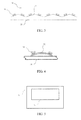
FIG. 3 is a schematic diagram of a portion of a MEMS device according to a third embodiment. -
FIG. 4 is a schematic diagram of an example of a movable member of the MEMS device inFIG. 3 . -
FIG. 5 shows an electronic apparatus with a MEMS device according to embodiments of this invention. - Various exemplary embodiments of the present invention will now be described in detail with reference to the drawings. It should be noted that the relative arrangement of the components and steps, the numerical expressions, and numerical values set forth in these embodiments do not limit the scope of the present invention unless it is specifically stated otherwise.
- The following description of at least one exemplary embodiment is merely illustrative in nature and is in no way intended to limit the invention, its application, or uses.
- Techniques, methods and apparatus as known by one of ordinary skill in the relevant art may not be discussed in detail but are intended to be part of the specification where appropriate.
- In all of the examples illustrated and discussed herein, any specific values should be interpreted to be illustrative only and non-limiting. Thus, other examples of the exemplary embodiments could have different values.
- Notice that similar reference numerals and letters refer to similar items in the following figures, and thus once an item is defined in one figure, it is possible that it need not be further discussed for following figures.
- In the embodiments of this invention, unlike the prior art, a micro-LED is provided on a movable member of a MEMS device so that a signal reflecting the movement of the movable member can easily be produced and/or detected. For example, the MEMS device is a MEMS chip.
- The embodiments and examples will be illustrated with reference to the figures.
-
FIG. 1 shows a schematic diagram of a portion of a MEMS device according to a first embodiment. - As shown in
FIG. 1 , theMEMS device 10 comprises a micro-LED 11 and amovable member 12. Themicro-LED 11 is mounted on themovable member 12 and is configured for moving with themovable member 12. Themovable member 12 can be any of cantilever, beam, plate, membrane, torsional plate, rotational platform and so on, for example. - Because the
micro-LED 11 can move according to the movement of themovable member 12, the light emitted by themicro-LED 11 can reflect the movement of themovable member 12. - As shown in
FIG. 1 , theMEMS device 10 further comprises at least oneoptical detector optical detector optical detector optical detector - In an example, the at least one
optical detector optical detector optical detector 13 c. The firstoptical detector 13 a or 13 is mounted to face the micro-LED 11 and is configured for sensing the light in the front of the micro-LED 11. The secondoptical detector 13 c is mounted in the lateral direction of the micro-LED 11 and is configured for sensing the light in the lateral direction of the micro-LED 11. - For example, the
movable member 12 is configured for moving according to the at least one of the following factors: acceleration of the MEMS device, angular speed of the MEMS device, pressure applied on the movable member, force applied on the movable member and flow applied on the movable member. The movement of themovable member 12 will cause a mechanical displacement of the micro-LED 11. The light emitted by the micro-LED 11 will displace along with the mechanical displacement of the micro-LED 11. The at least oneoptical detector - In such a configuration, the MEMS device can easily convert these physical quantities into a light signal and/or an electronic signal.
- For example, the micro-LED size is 1-100 μm in side length and 1-10 μm in thickness. The micro-LED can emitted red light, green light, blue light or UV, etc.
- As shown in
FIG. 1 , themovable member 12 is mounted on asubstrate 14. Thesubstrate 14 can be any of silicon, other semiconductor, glass, ceramic, quartz, sapphire, etc. Theoptical detectors cap 15. Thus, thecap 15 is a detector. Thecap 15 is connected with thesubstrate 14 via abond line 17. Theoptical detector 13 c is mounted on anothersubstrate 16, which can also be called a detector. Thedetector 16 is connected with thecap 15 via abond line 18. - In this embodiment, the micro-LED is used to produce signals reflecting the movement of a movable member of a MEMS device. This configuration simplifies the signal detection of a MEMS device and/or enriches the contents of signals produced by the MEMS device.
-
FIG. 2 is a schematic diagram of a portion of a MEMS device according to a second embodiment. The repetitive contents with the first embodiment will be omitted. - As shown in
FIG. 2 , theMEMS device 20 comprises a micro-LED 21 and amovable member 22. The micro-LED 21 is mounted on themovable member 22 and is configured for moving with themovable member 22. - The
movable member 22 is supported by thesupport member 23. Thesupport member 23 is mounted on thesubstrate 26. - In this embodiment, the
MEMS device 20 can be used as a modulator. For example, themovable member 22 is configured for being actuated to move by an electronic signal or electromagnetic signal applied thereon. The electronic signal or electromagnetic signal can be applied through thesupport substrate 23 and thesubstrate 26. The micro-LED 21 is configured for emitting a light signal modulated by the movement of the movable member. - For example, the modulated light signal is directly fed into an
optic fiber 25. For example, as shown inFIG. 2 , acoupler 24 is provided on thesubstrate 26 and is used to couple or feed the modulated light signal into anoptic fiber 25. - It will be appreciated by a person skilled in the art that although
FIG. 2 shows a light modulation, thecoupler 24 can be replaced by an optical detector, such as a photo diode, and theoptic fiber 25 can be replaced by a wire. In such a situation, the modulated signal can be an electronic signal and be transmitted by the wire. - This embodiment provides a new solution of modulation. By this embodiment, a new MEMS modulator can be provided.
-
FIG. 3 is a schematic diagram of a portion of a MEMS device according to a third embodiment. The repetitive contents with the first embodiment will be omitted. - As shown in
FIG. 3 , theMEMS device 30 comprises a plurality of micro-LEDs 31 and a plurality ofmovable members 32. The plurality of the micro-LEDs 31 are mounted on the plurality of themovable members 32 on adisplay panel 33, respectively. - The plurality of the
movable members 32 are configured for moving to form angles with the plane of thedisplay panel 33, respectively, so that the light emitted by the plurality of the micro-LEDs 31 form a 3D image. - A person skilled in the art can conceive many approaches for forming such
movable members 32. An example of suchmovable members 32 will be illustrated with reference toFIG. 4 .FIG. 4 shows a schematic diagram of an example of a movable member of the MEMS device inFIG. 3 . - As shown in
FIG. 4 , themovable member 32′ can be of electrostriction material, for example. Themovable member 32′ can be deformed under electronic signal so that the angles of themovable members 32′ (and thus the micro-LEDs 31′) with respect to thedisplay panel 33′ can be adjusted. - Through adjusting the angles of the micro-LEDs 31′ with respect to the
display panel 33′, a 3D image can be produced. - This embodiment provides a new solution for 3D display.
-
FIG. 5 shows an electronic apparatus with a MEMS device according to embodiments of this invention. - As shown in
FIG. 5 , theelectronic apparatus 40 comprises aMEMS device 41. TheMEMS device 41 can be any of the MEMS devices shown inFIGS. 1, 2 and 3 . - As such, the
electronic apparatus 40 could be a detector for detecting acceleration, angular speed, pressure, force or flow, etc. Alternatively, theelectronic apparatus 40 could be a modulator for modulating light and/or electronic signal. Alternatively, theelectronic apparatus 40 could be a display apparatus for displaying a 3D image. - In the embodiments of this invention, a MEMS device with a micro-LED mounted on a movable member thereof is provided, so that the signal detection of a MEMS device is simplified and/or the contents of signals produced by the MEMS device is enriched.
- Although some specific embodiments of the present invention have been demonstrated in detail with examples, it should be understood by a person skilled in the art that the above examples are only intended to be illustrative but not to limit the scope of the present invention. It should be understood by a person skilled in the art that the above embodiments can be modified without departing from the scope and spirit of the present invention. The scope of the present invention is defined by the attached claims.
Claims (10)
Applications Claiming Priority (1)
| Application Number | Priority Date | Filing Date | Title |
|---|---|---|---|
| PCT/CN2016/084544 WO2017206149A1 (en) | 2016-06-02 | 2016-06-02 | Mems device and electronic apparatus |
Publications (2)
| Publication Number | Publication Date |
|---|---|
| US20190079110A1 true US20190079110A1 (en) | 2019-03-14 |
| US11262376B2 US11262376B2 (en) | 2022-03-01 |
Family
ID=60478314
Family Applications (1)
| Application Number | Title | Priority Date | Filing Date |
|---|---|---|---|
| US16/078,213 Active 2036-12-01 US11262376B2 (en) | 2016-06-02 | 2016-06-02 | MEMS device and electronic apparatus |
Country Status (3)
| Country | Link |
|---|---|
| US (1) | US11262376B2 (en) |
| CN (1) | CN108698813B (en) |
| WO (1) | WO2017206149A1 (en) |
Citations (5)
| Publication number | Priority date | Publication date | Assignee | Title |
|---|---|---|---|---|
| US5689107A (en) * | 1995-09-01 | 1997-11-18 | Hughes Aircraft Company | Displacement-based opto-electronic accelerometer and pressure sensor |
| US6494095B1 (en) * | 2000-03-28 | 2002-12-17 | Opticnet, Inc. | Micro electromechanical switch for detecting acceleration or decelaration |
| US20090174885A1 (en) * | 2008-01-03 | 2009-07-09 | Chian Chiu Li | Sensor And Method Utilizing Multiple Optical Interferometers |
| US8426227B1 (en) * | 2011-11-18 | 2013-04-23 | LuxVue Technology Corporation | Method of forming a micro light emitting diode array |
| US20150338246A1 (en) * | 2014-05-26 | 2015-11-26 | Commissariat A L'energie Atomique Et Aux Energies Alternatives | Capacitive microelectronic and/or nanoelectronic device with increased compactness |
Family Cites Families (15)
| Publication number | Priority date | Publication date | Assignee | Title |
|---|---|---|---|---|
| IL130045A0 (en) * | 1999-05-19 | 2000-02-29 | Univ Ramot | Micromachined displacement sensors and actuators |
| US7199354B2 (en) * | 2004-08-26 | 2007-04-03 | Dr. Johannes Heidenhain Gmbh | Detector array for optical encoders |
| CN2844881Y (en) * | 2005-03-15 | 2006-12-06 | 陆轻锂 | High sensitive vibration detector |
| KR100815440B1 (en) | 2006-07-28 | 2008-03-20 | 주식회사 나노브릭 | Optical projection engine based on micro-electromechanical system and its manufacturing method |
| EP2053400A1 (en) * | 2007-10-22 | 2009-04-29 | Consejo Superior De Investigaciones Cientificas | Method and system for detection of a selected type of molecules in a sample |
| US7609136B2 (en) * | 2007-12-20 | 2009-10-27 | General Electric Company | MEMS microswitch having a conductive mechanical stop |
| KR101039881B1 (en) * | 2009-12-21 | 2011-06-09 | 엘지이노텍 주식회사 | Light emitting element and light unit using same |
| US8646505B2 (en) * | 2011-11-18 | 2014-02-11 | LuxVue Technology Corporation | Micro device transfer head |
| US8791530B2 (en) * | 2012-09-06 | 2014-07-29 | LuxVue Technology Corporation | Compliant micro device transfer head with integrated electrode leads |
| US9391042B2 (en) * | 2012-12-14 | 2016-07-12 | Apple Inc. | Micro device transfer system with pivot mount |
| US9087764B2 (en) | 2013-07-26 | 2015-07-21 | LuxVue Technology Corporation | Adhesive wafer bonding with controlled thickness variation |
| US9659717B2 (en) * | 2014-02-18 | 2017-05-23 | Analog Devices Global | MEMS device with constant capacitance |
| US20160140685A1 (en) | 2014-11-17 | 2016-05-19 | Pixtronix, Inc. | Display including sensors |
| US10141287B2 (en) * | 2015-07-14 | 2018-11-27 | Goertek, Inc. | Transferring method, manufacturing method, device and electronic apparatus of micro-LED |
| CN112822840B (en) * | 2015-08-20 | 2026-02-24 | 苹果公司 | Fabric-based article with an array of electronic components |
-
2016
- 2016-06-02 US US16/078,213 patent/US11262376B2/en active Active
- 2016-06-02 CN CN201680078846.4A patent/CN108698813B/en active Active
- 2016-06-02 WO PCT/CN2016/084544 patent/WO2017206149A1/en not_active Ceased
Patent Citations (5)
| Publication number | Priority date | Publication date | Assignee | Title |
|---|---|---|---|---|
| US5689107A (en) * | 1995-09-01 | 1997-11-18 | Hughes Aircraft Company | Displacement-based opto-electronic accelerometer and pressure sensor |
| US6494095B1 (en) * | 2000-03-28 | 2002-12-17 | Opticnet, Inc. | Micro electromechanical switch for detecting acceleration or decelaration |
| US20090174885A1 (en) * | 2008-01-03 | 2009-07-09 | Chian Chiu Li | Sensor And Method Utilizing Multiple Optical Interferometers |
| US8426227B1 (en) * | 2011-11-18 | 2013-04-23 | LuxVue Technology Corporation | Method of forming a micro light emitting diode array |
| US20150338246A1 (en) * | 2014-05-26 | 2015-11-26 | Commissariat A L'energie Atomique Et Aux Energies Alternatives | Capacitive microelectronic and/or nanoelectronic device with increased compactness |
Also Published As
| Publication number | Publication date |
|---|---|
| CN108698813B (en) | 2023-01-20 |
| WO2017206149A1 (en) | 2017-12-07 |
| CN108698813A (en) | 2018-10-23 |
| US11262376B2 (en) | 2022-03-01 |
Similar Documents
| Publication | Publication Date | Title |
|---|---|---|
| US11906726B2 (en) | Micromachined mirror assembly having micro mirror array and hybrid driving method thereof | |
| US20080095531A1 (en) | Device and method for inspecting optical modulator | |
| CN105940669B (en) | camera device | |
| US8994927B2 (en) | Device for measuring a distance to a target object | |
| CN109994413A (en) | Micro element flood tide transfer method | |
| Hofmann et al. | Wafer-level vacuum packaged resonant micro-scanning mirrors for compact laser projection displays | |
| US11262376B2 (en) | MEMS device and electronic apparatus | |
| US11340131B2 (en) | Multi-hole probe pressure sensors | |
| JP2009098003A (en) | Vibration displacement detecting device and method of detecting displacement and vibration | |
| US8619259B2 (en) | High-speed optical measurement apparatus | |
| US11899136B2 (en) | Increasing VCSEL projector spatial resolution | |
| CN105093774A (en) | MEMS micro-mirror, display panel and display device | |
| TWI783331B (en) | Head-up display for vehicle with multiple projecting screens | |
| Langa et al. | Wafer level vacuum packaging of scanning micro-mirrors using glass-frit and anodic bonding methods | |
| US10948153B2 (en) | Lighting apparatus and light module | |
| JP2019105577A (en) | Doppler lidar device and air turbulence alarm system | |
| CN201583285U (en) | Photoelectric transducer | |
| EP0216812A1 (en) | MEASURING DEVICE. | |
| Schenk et al. | Ultra compact laser based projectors and imagers | |
| US20180366902A1 (en) | Laser projector with angled reflector | |
| RU167677U1 (en) | Photoelectric Pressure Sensor | |
| Yi et al. | A cascaded line imager using single-pixel detectors | |
| RU2573708C1 (en) | Amplitude fibre-optic pressure sensor | |
| Koh et al. | 3-D MEMS VOA using electromagnetic and electrothermal actuations | |
| US20160124124A1 (en) | Optic apparatus |
Legal Events
| Date | Code | Title | Description |
|---|---|---|---|
| FEPP | Fee payment procedure |
Free format text: ENTITY STATUS SET TO UNDISCOUNTED (ORIGINAL EVENT CODE: BIG.); ENTITY STATUS OF PATENT OWNER: LARGE ENTITY |
|
| AS | Assignment |
Owner name: GOERTEK INC., CHINA Free format text: ASSIGNMENT OF ASSIGNORS INTEREST;ASSIGNOR:ZOU, QUANBO;REEL/FRAME:046708/0874 Effective date: 20180814 |
|
| STPP | Information on status: patent application and granting procedure in general |
Free format text: DOCKETED NEW CASE - READY FOR EXAMINATION |
|
| STPP | Information on status: patent application and granting procedure in general |
Free format text: NON FINAL ACTION MAILED |
|
| STPP | Information on status: patent application and granting procedure in general |
Free format text: RESPONSE TO NON-FINAL OFFICE ACTION ENTERED AND FORWARDED TO EXAMINER |
|
| STPP | Information on status: patent application and granting procedure in general |
Free format text: NON FINAL ACTION MAILED |
|
| STPP | Information on status: patent application and granting procedure in general |
Free format text: RESPONSE TO NON-FINAL OFFICE ACTION ENTERED AND FORWARDED TO EXAMINER |
|
| AS | Assignment |
Owner name: WEIFANG GOERTEK MICROELECTRONICS CO., LTD., CHINA Free format text: ASSIGNMENT OF ASSIGNORS INTEREST;ASSIGNOR:GOERTEK, INC.;REEL/FRAME:052846/0443 Effective date: 20200605 |
|
| STPP | Information on status: patent application and granting procedure in general |
Free format text: RESPONSE TO NON-FINAL OFFICE ACTION ENTERED AND FORWARDED TO EXAMINER |
|
| STPP | Information on status: patent application and granting procedure in general |
Free format text: NON FINAL ACTION MAILED |
|
| STPP | Information on status: patent application and granting procedure in general |
Free format text: RESPONSE TO NON-FINAL OFFICE ACTION ENTERED AND FORWARDED TO EXAMINER |
|
| STPP | Information on status: patent application and granting procedure in general |
Free format text: NOTICE OF ALLOWANCE MAILED -- APPLICATION RECEIVED IN OFFICE OF PUBLICATIONS |
|
| STCF | Information on status: patent grant |
Free format text: PATENTED CASE |
|
| MAFP | Maintenance fee payment |
Free format text: PAYMENT OF MAINTENANCE FEE, 4TH YEAR, LARGE ENTITY (ORIGINAL EVENT CODE: M1551); ENTITY STATUS OF PATENT OWNER: LARGE ENTITY Year of fee payment: 4 |