US20180348564A1 - Liquid crystal cell and manufacturing method thereof - Google Patents
Liquid crystal cell and manufacturing method thereof Download PDFInfo
- Publication number
- US20180348564A1 US20180348564A1 US15/726,396 US201715726396A US2018348564A1 US 20180348564 A1 US20180348564 A1 US 20180348564A1 US 201715726396 A US201715726396 A US 201715726396A US 2018348564 A1 US2018348564 A1 US 2018348564A1
- Authority
- US
- United States
- Prior art keywords
- substrate
- liquid crystal
- support pillars
- crystal cell
- cell according
- Prior art date
- Legal status (The legal status is an assumption and is not a legal conclusion. Google has not performed a legal analysis and makes no representation as to the accuracy of the status listed.)
- Granted
Links
- 239000004973 liquid crystal related substance Substances 0.000 title claims abstract description 136
- 210000002858 crystal cell Anatomy 0.000 title claims abstract description 93
- 238000004519 manufacturing process Methods 0.000 title claims description 24
- 239000000758 substrate Substances 0.000 claims abstract description 302
- 239000000463 material Substances 0.000 claims abstract description 19
- 210000004027 cell Anatomy 0.000 claims abstract description 12
- 238000005530 etching Methods 0.000 claims description 14
- 239000004642 Polyimide Substances 0.000 claims description 6
- 239000004743 Polypropylene Substances 0.000 claims description 6
- 229920001721 polyimide Polymers 0.000 claims description 6
- 229920001155 polypropylene Polymers 0.000 claims description 6
- 239000004793 Polystyrene Substances 0.000 claims description 3
- 239000011521 glass Substances 0.000 claims description 3
- -1 polypropylene Polymers 0.000 claims description 3
- 229910052710 silicon Inorganic materials 0.000 claims description 3
- 239000010703 silicon Substances 0.000 claims description 3
- 238000000034 method Methods 0.000 description 12
- 125000006850 spacer group Chemical group 0.000 description 12
- 230000003287 optical effect Effects 0.000 description 9
- 230000008569 process Effects 0.000 description 8
- 239000000853 adhesive Substances 0.000 description 4
- 230000001070 adhesive effect Effects 0.000 description 4
- 230000007547 defect Effects 0.000 description 2
- 238000012986 modification Methods 0.000 description 2
- 230000004048 modification Effects 0.000 description 2
- 229920002120 photoresistant polymer Polymers 0.000 description 2
- 230000002159 abnormal effect Effects 0.000 description 1
- 230000004075 alteration Effects 0.000 description 1
- 230000008901 benefit Effects 0.000 description 1
- 230000008859 change Effects 0.000 description 1
- 238000003486 chemical etching Methods 0.000 description 1
- 239000003086 colorant Substances 0.000 description 1
- 230000000694 effects Effects 0.000 description 1
- 238000001459 lithography Methods 0.000 description 1
- 238000000059 patterning Methods 0.000 description 1
- 239000011347 resin Substances 0.000 description 1
- 229920005989 resin Polymers 0.000 description 1
Images


Classifications
-
- G—PHYSICS
- G02—OPTICS
- G02F—OPTICAL DEVICES OR ARRANGEMENTS FOR THE CONTROL OF LIGHT BY MODIFICATION OF THE OPTICAL PROPERTIES OF THE MEDIA OF THE ELEMENTS INVOLVED THEREIN; NON-LINEAR OPTICS; FREQUENCY-CHANGING OF LIGHT; OPTICAL LOGIC ELEMENTS; OPTICAL ANALOGUE/DIGITAL CONVERTERS
- G02F1/00—Devices or arrangements for the control of the intensity, colour, phase, polarisation or direction of light arriving from an independent light source, e.g. switching, gating or modulating; Non-linear optics
- G02F1/01—Devices or arrangements for the control of the intensity, colour, phase, polarisation or direction of light arriving from an independent light source, e.g. switching, gating or modulating; Non-linear optics for the control of the intensity, phase, polarisation or colour
- G02F1/13—Devices or arrangements for the control of the intensity, colour, phase, polarisation or direction of light arriving from an independent light source, e.g. switching, gating or modulating; Non-linear optics for the control of the intensity, phase, polarisation or colour based on liquid crystals, e.g. single liquid crystal display cells
- G02F1/133—Constructional arrangements; Operation of liquid crystal cells; Circuit arrangements
- G02F1/1333—Constructional arrangements; Manufacturing methods
- G02F1/1339—Gaskets; Spacers; Sealing of cells
- G02F1/13394—Gaskets; Spacers; Sealing of cells spacers regularly patterned on the cell subtrate, e.g. walls, pillars
-
- G—PHYSICS
- G02—OPTICS
- G02F—OPTICAL DEVICES OR ARRANGEMENTS FOR THE CONTROL OF LIGHT BY MODIFICATION OF THE OPTICAL PROPERTIES OF THE MEDIA OF THE ELEMENTS INVOLVED THEREIN; NON-LINEAR OPTICS; FREQUENCY-CHANGING OF LIGHT; OPTICAL LOGIC ELEMENTS; OPTICAL ANALOGUE/DIGITAL CONVERTERS
- G02F1/00—Devices or arrangements for the control of the intensity, colour, phase, polarisation or direction of light arriving from an independent light source, e.g. switching, gating or modulating; Non-linear optics
- G02F1/01—Devices or arrangements for the control of the intensity, colour, phase, polarisation or direction of light arriving from an independent light source, e.g. switching, gating or modulating; Non-linear optics for the control of the intensity, phase, polarisation or colour
- G02F1/13—Devices or arrangements for the control of the intensity, colour, phase, polarisation or direction of light arriving from an independent light source, e.g. switching, gating or modulating; Non-linear optics for the control of the intensity, phase, polarisation or colour based on liquid crystals, e.g. single liquid crystal display cells
- G02F1/133—Constructional arrangements; Operation of liquid crystal cells; Circuit arrangements
- G02F1/1333—Constructional arrangements; Manufacturing methods
- G02F1/1341—Filling or closing of cells
-
- G—PHYSICS
- G02—OPTICS
- G02F—OPTICAL DEVICES OR ARRANGEMENTS FOR THE CONTROL OF LIGHT BY MODIFICATION OF THE OPTICAL PROPERTIES OF THE MEDIA OF THE ELEMENTS INVOLVED THEREIN; NON-LINEAR OPTICS; FREQUENCY-CHANGING OF LIGHT; OPTICAL LOGIC ELEMENTS; OPTICAL ANALOGUE/DIGITAL CONVERTERS
- G02F1/00—Devices or arrangements for the control of the intensity, colour, phase, polarisation or direction of light arriving from an independent light source, e.g. switching, gating or modulating; Non-linear optics
- G02F1/29—Devices or arrangements for the control of the intensity, colour, phase, polarisation or direction of light arriving from an independent light source, e.g. switching, gating or modulating; Non-linear optics for the control of the position or the direction of light beams, i.e. deflection
-
- G—PHYSICS
- G02—OPTICS
- G02F—OPTICAL DEVICES OR ARRANGEMENTS FOR THE CONTROL OF LIGHT BY MODIFICATION OF THE OPTICAL PROPERTIES OF THE MEDIA OF THE ELEMENTS INVOLVED THEREIN; NON-LINEAR OPTICS; FREQUENCY-CHANGING OF LIGHT; OPTICAL LOGIC ELEMENTS; OPTICAL ANALOGUE/DIGITAL CONVERTERS
- G02F1/00—Devices or arrangements for the control of the intensity, colour, phase, polarisation or direction of light arriving from an independent light source, e.g. switching, gating or modulating; Non-linear optics
- G02F1/01—Devices or arrangements for the control of the intensity, colour, phase, polarisation or direction of light arriving from an independent light source, e.g. switching, gating or modulating; Non-linear optics for the control of the intensity, phase, polarisation or colour
- G02F1/13—Devices or arrangements for the control of the intensity, colour, phase, polarisation or direction of light arriving from an independent light source, e.g. switching, gating or modulating; Non-linear optics for the control of the intensity, phase, polarisation or colour based on liquid crystals, e.g. single liquid crystal display cells
- G02F1/133—Constructional arrangements; Operation of liquid crystal cells; Circuit arrangements
- G02F1/1333—Constructional arrangements; Manufacturing methods
- G02F1/133302—Rigid substrates, e.g. inorganic substrates
-
- G—PHYSICS
- G02—OPTICS
- G02F—OPTICAL DEVICES OR ARRANGEMENTS FOR THE CONTROL OF LIGHT BY MODIFICATION OF THE OPTICAL PROPERTIES OF THE MEDIA OF THE ELEMENTS INVOLVED THEREIN; NON-LINEAR OPTICS; FREQUENCY-CHANGING OF LIGHT; OPTICAL LOGIC ELEMENTS; OPTICAL ANALOGUE/DIGITAL CONVERTERS
- G02F1/00—Devices or arrangements for the control of the intensity, colour, phase, polarisation or direction of light arriving from an independent light source, e.g. switching, gating or modulating; Non-linear optics
- G02F1/01—Devices or arrangements for the control of the intensity, colour, phase, polarisation or direction of light arriving from an independent light source, e.g. switching, gating or modulating; Non-linear optics for the control of the intensity, phase, polarisation or colour
- G02F1/13—Devices or arrangements for the control of the intensity, colour, phase, polarisation or direction of light arriving from an independent light source, e.g. switching, gating or modulating; Non-linear optics for the control of the intensity, phase, polarisation or colour based on liquid crystals, e.g. single liquid crystal display cells
- G02F1/133—Constructional arrangements; Operation of liquid crystal cells; Circuit arrangements
- G02F1/1333—Constructional arrangements; Manufacturing methods
- G02F1/133305—Flexible substrates, e.g. plastics, organic film
-
- G—PHYSICS
- G02—OPTICS
- G02F—OPTICAL DEVICES OR ARRANGEMENTS FOR THE CONTROL OF LIGHT BY MODIFICATION OF THE OPTICAL PROPERTIES OF THE MEDIA OF THE ELEMENTS INVOLVED THEREIN; NON-LINEAR OPTICS; FREQUENCY-CHANGING OF LIGHT; OPTICAL LOGIC ELEMENTS; OPTICAL ANALOGUE/DIGITAL CONVERTERS
- G02F1/00—Devices or arrangements for the control of the intensity, colour, phase, polarisation or direction of light arriving from an independent light source, e.g. switching, gating or modulating; Non-linear optics
- G02F1/01—Devices or arrangements for the control of the intensity, colour, phase, polarisation or direction of light arriving from an independent light source, e.g. switching, gating or modulating; Non-linear optics for the control of the intensity, phase, polarisation or colour
- G02F1/13—Devices or arrangements for the control of the intensity, colour, phase, polarisation or direction of light arriving from an independent light source, e.g. switching, gating or modulating; Non-linear optics for the control of the intensity, phase, polarisation or colour based on liquid crystals, e.g. single liquid crystal display cells
- G02F1/133—Constructional arrangements; Operation of liquid crystal cells; Circuit arrangements
- G02F1/1333—Constructional arrangements; Manufacturing methods
- G02F1/1339—Gaskets; Spacers; Sealing of cells
- G02F1/13396—Spacers having different sizes
-
- G—PHYSICS
- G02—OPTICS
- G02F—OPTICAL DEVICES OR ARRANGEMENTS FOR THE CONTROL OF LIGHT BY MODIFICATION OF THE OPTICAL PROPERTIES OF THE MEDIA OF THE ELEMENTS INVOLVED THEREIN; NON-LINEAR OPTICS; FREQUENCY-CHANGING OF LIGHT; OPTICAL LOGIC ELEMENTS; OPTICAL ANALOGUE/DIGITAL CONVERTERS
- G02F1/00—Devices or arrangements for the control of the intensity, colour, phase, polarisation or direction of light arriving from an independent light source, e.g. switching, gating or modulating; Non-linear optics
- G02F1/01—Devices or arrangements for the control of the intensity, colour, phase, polarisation or direction of light arriving from an independent light source, e.g. switching, gating or modulating; Non-linear optics for the control of the intensity, phase, polarisation or colour
- G02F1/13—Devices or arrangements for the control of the intensity, colour, phase, polarisation or direction of light arriving from an independent light source, e.g. switching, gating or modulating; Non-linear optics for the control of the intensity, phase, polarisation or colour based on liquid crystals, e.g. single liquid crystal display cells
- G02F1/133—Constructional arrangements; Operation of liquid crystal cells; Circuit arrangements
- G02F1/1333—Constructional arrangements; Manufacturing methods
- G02F1/1339—Gaskets; Spacers; Sealing of cells
- G02F1/13398—Spacer materials; Spacer properties
-
- G—PHYSICS
- G02—OPTICS
- G02F—OPTICAL DEVICES OR ARRANGEMENTS FOR THE CONTROL OF LIGHT BY MODIFICATION OF THE OPTICAL PROPERTIES OF THE MEDIA OF THE ELEMENTS INVOLVED THEREIN; NON-LINEAR OPTICS; FREQUENCY-CHANGING OF LIGHT; OPTICAL LOGIC ELEMENTS; OPTICAL ANALOGUE/DIGITAL CONVERTERS
- G02F1/00—Devices or arrangements for the control of the intensity, colour, phase, polarisation or direction of light arriving from an independent light source, e.g. switching, gating or modulating; Non-linear optics
- G02F1/29—Devices or arrangements for the control of the intensity, colour, phase, polarisation or direction of light arriving from an independent light source, e.g. switching, gating or modulating; Non-linear optics for the control of the position or the direction of light beams, i.e. deflection
- G02F1/294—Variable focal length devices
-
- G02F2001/13396—
-
- G02F2001/13398—
Definitions
- the invention generally relates an optical element and a manufacturing method thereof, and, in particular, to a liquid crystal cell and a manufacturing method thereof.
- a liquid crystal lens is commonly used as an electrically tunable lens since the liquid crystal cell can function as a lens by controlling the orientations of liquid crystals to change the effective refractive powers thereof.
- Uniform cell gap of the liquid crystal cell can make the optical properties of the liquid crystals stable and can prevent abnormal colors and optical aberration.
- photoresist is used to form pillars with the specific height and density as the spacers of the liquid crystal cell, which is a common design for the process of liquid crystal displays.
- the cell gap of the liquid crystal lens is much larger than one of the liquid crystal display. As a result, the cell gap of the liquid crystal lens is too large to form the spacers made of the photoresist.
- the invention provides a liquid crystal cell capable of maintaining a stable cell gap.
- the invention provides a manufacturing method of a liquid crystal cell, which is capable of manufacturing a liquid crystal cell that can maintain a stable cell gap.
- a liquid crystal cell including a first substrate, a second substrate, a liquid crystal layer and a plurality of first support pillars.
- the first substrate has a first surface and a second surface. The second surface is opposite to the first surface.
- the second substrate is disposed beside the first substrate and has a third surface and a fourth surface. The forth surface is opposite to the third surface.
- the first surface of the first substrate and the third surface of the second substrate face each other.
- the liquid crystal layer is disposed between the first substrate and the second substrate.
- the plurality of first support pillars are configured to form a cell gap of the liquid crystal cell and disposed on the first surface of the first substrate, wherein the first substrate and the plurality of first support pillars are integrally formed and made of a same material.
- a manufacturing method of a liquid crystal cell includes providing a first substrate having a first surface and a second surface opposite to the first substrate; providing a second substrate having a third surface and a fourth surface opposite to the third substrate; etching the first surface of the first substrate to form a plurality of first support pillars; filling liquid crystals into a gap between the first substrate and the second substrate to form a liquid crystal layer; and bonding the first substrate and the second substrate and causing the first surface of the first substrate and the third surface of the second substrate to face each other.
- the plurality of first support pillars with specific height are easily formed as the spacers of the liquid crystal cell. Since the plurality of first support pillars and the first substrate are integrally formed and made of the same material, the plurality of first support pillars are firm enough to resist the following high-temperature processes or external force applied and have relatively minor influences on the optical performance. In addition, the problems of insufficient adhesive strength between two materials, inadequate supporting strength of the spacers, and pollution of the liquid crystals due to contact with the spacers can be solved.
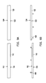
- FIG. 1A is a schematic cross-sectional view of a liquid crystal cell according to an embodiment of the invention.
- FIG. 1B is a schematic partial enlarged view corresponding to a region R of FIG. 1A .
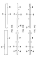
- FIG. 2 is a schematic cross-sectional view of a liquid crystal cell according to an embodiment of the invention.
- FIG. 3 is a schematic cross-sectional view of a liquid crystal cell according to another embodiment of the invention.
- FIG. 4 is a schematic cross-sectional view of a liquid crystal cell according to an embodiment of the invention.
- FIG. 5 , FIG. 6 , and FIG. 7 are schematic cross-sectional views of liquid crystal cells according to other embodiments of the invention.
- FIG. 8A to FIG. 8D are cross-sectional views illustrating a manufacturing process for a liquid crystal cell according to an embodiment of the invention.
- FIG. 9A to FIG. 9E are cross-sectional views illustrating manufacturing processes for a liquid crystal cell according to other embodiments of the invention.
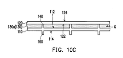
- FIG. 10A to FIG. 10C are cross-sectional views illustrating a manufacturing process for a liquid crystal cell according to another embodiments of the invention.
- FIG. 11A to FIG. 11E are cross-sectional views illustrating manufacturing processes for a liquid crystal cell according to other embodiments of the invention.
- FIG. 12A to FIG. 12C are cross-sectional views illustrating a manufacturing process for a liquid crystal cell according to another embodiment of the invention.
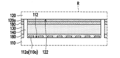
- FIG. 1A is a schematic cross-sectional view of a liquid crystal cell according to an embodiment of the invention.
- a liquid crystal cell 100 of the present embodiment includes a first substrate 110 , a second substrate 120 , a liquid crystal layer 130 and a plurality of first support pillars 140 .
- the first substrate 110 has a first surface 112 and a second surface 114 .
- the second surface 114 is opposite to the first surface 112 .
- the second substrate 120 is disposed beside the first substrate 110 and has a third surface 122 and a fourth surface 124 .
- the forth surface 124 is opposite to the third surface 122 .
- the first surface 112 of the first substrate 110 and the third surface 122 of the second substrate 120 face each other.
- the liquid crystal layer 130 is disposed between the first substrate 110 and the second substrate 120 .
- the plurality of first support pillars 140 are configured to form a cell gap G of the liquid crystal cell 100 and disposed on the first surface 112 of the first substrate 110 , wherein the first substrate 110 and the plurality of first support pillars 140 are integrally formed and made of a same material.
- the materials of the first substrate 110 and second substrate 120 may include glass, polyimide (PI), polystyrene (PS), polypropylene (PP), or silicon, for example.
- the liquid crystal cell 100 may be a liquid crystal display, a liquid crystal lens, or a liquid crystal filter.
- the plurality of first support pillars 140 and the first substrate 110 are integrally formed and made of the same material, the plurality of first support pillars 140 are firm enough to resist the following high-temperature processes or external force applied and have relatively minor influences on the optical performance.
- the problems of insufficient adhesive strength between two materials, inadequate supporting strength of the spacers, and pollution of the liquid crystals due to contact with the spacers can be solved.
- a height H1 of the plurality of first support pillars 140 ranges from 2 ⁇ m to 50 ⁇ m.
- the height H1 of the plurality of first support pillars 140 may range from 2 ⁇ m to 5 ⁇ m, for example.
- the height H1 of the plurality of first support pillars 140 may range from 10 ⁇ m to 50 ⁇ m, for example.
- the height H1 of the plurality of first support pillars 140 may range from 3 ⁇ m to 5 ⁇ m, for example.
- FIG. 1B is a schematic partial enlarged view corresponding to a region R of FIG. 1A .
- the liquid crystal cell 100 of the present embodiment further includes a first electrode layer 110 a , a second electrode layer 120 a , and two alignment layers 180 .
- the first electrode layer 110 a is disposed on the first surface 112 of the first substrate 110 .
- the second electrode layer 120 a is disposed on the third surface 122 of the second substrate 120 .
- One of the alignment layers 180 is disposed between the first electrode layer 110 a and the liquid crystal layer 130 .
- the other alignment layer 180 is disposed between the second electrode layer 120 a and the liquid crystal layer 130 .
- the first electrode layer 110 a includes a plurality of first electrodes 112 a which are discrete to each other, and the second electrode layer 120 a includes a common electrode.
- the first electrode layer 110 a can include a common electrode
- the second electrode layer 120 a can include a plurality of first electrodes which are discrete to each other.
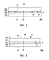
- FIG. 2 is a schematic cross-sectional view of a liquid crystal cell according to an embodiment of the invention.
- FIG. 3 is a schematic cross-sectional view of a liquid crystal cell according to another embodiment of the invention.
- a liquid crystal cell 100 a and a liquid crystal cell 100 b of those embodiments are substantially similar to the liquid crystal cell 100 , and the differences therebetween are as follows.
- the liquid crystal cell 100 a and the liquid crystal cell 100 b further include a plurality of second support pillars 150 disposed on one of the third surface 122 and the fourth surface 124 of the second substrate 120 , wherein the second substrate 120 and the plurality of second support pillars 150 are integrally formed and made of a same material. As illustrated in FIG.
- the plurality of second support pillars 150 are disposed on the third surface 122 of the second substrate 120 . As illustrated in FIG. 3 , the plurality of second support pillars 150 are disposed on the forth surface 124 of the second substrate 120 . In the embodiment as illustrated in FIG. 2 , since the plurality of first support pillars 140 and the plurality of second support pillars 150 are disposed on the first surface 112 of the first substrate 110 and the third surface 122 of the second substrate 120 , respectively, the ability of controlling the cell gap is more precise.
- the height H1 of the plurality of the first support pillars 140 and a height H2 of the plurality of the second support pillars 150 can be the same. In other embodiments of the invention, the height H1 of the plurality of the first support pillars 140 and the height H2 of the plurality of the second support pillars 150 can be different.
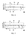
- FIG. 4 is a schematic cross-sectional view of a liquid crystal cell according to an embodiment of the invention.
- a liquid crystal cell 100 c of the present embodiment is substantially similar to the liquid crystal cell 100 , and the difference therebetween is as follows.
- the liquid crystal cell 100 c further includes a plurality of second support pillars 160 disposed on the second surface 114 of the first substrate 110 , wherein the first substrate 110 and the plurality of second support pillars 160 are integrally formed and made of a same material.
- FIG. 5 , FIG. 6 , and FIG. 7 are schematic cross-sectional views of liquid crystal cells according to other embodiments of the invention.
- a liquid crystal cell 100 d , a liquid crystal cell 100 e , and a liquid crystal cell 100 f of the present embodiments are substantially similar to the liquid crystal cell 100 c , and the differences therebetween are as follows.
- the liquid crystal cell 100 d , the liquid crystal cell 100 e , and the liquid crystal cell 100 f further include a plurality of third support pillars 170 disposed on at least one of the third surface 122 and the fourth surface 124 of the second substrate 120 , wherein the second substrate 120 and the plurality of third support pillars 170 are integrally formed and made of a same material.
- the plurality of third support pillars 170 are disposed on the third surface 122 of the second substrate 120 .
- the plurality of third support pillars 170 are disposed on the fourth surface 124 of the second substrate 120 .
- the plurality of third support pillars 170 are disposed on both of the third surface 122 and the fourth surface 124 of the second substrate 120 .
- the height H1 of the plurality of the first support pillars 140 and a height H3 of the plurality of the third support pillars 170 can be the same. In other embodiments of the invention, the height H1 of the plurality of the first support pillars 140 and the height H3 of the plurality of the third support pillars 170 can be different.
- liquid crystal cells in the embodiments of the invention as mentioned previously can be bonded together to form a stacked structure.
- one liquid crystal cell 100 b can be bonded to another liquid crystal cell 100 b , one liquid crystal cell 100 c , two liquid crystal cells 100 c , or one liquid crystal cell 100 c and one liquid crystal cell 100 d , but the invention is not limited thereto.
- the plurality of the second support pillars 150 disposed on the fourth surface 124 of the second substrate 120 , the plurality of the second support pillars 160 disposed on the second surface 114 of the first substrate 110 , or the plurality of the third support pillars 170 disposed on the fourth surface 124 of the second substrate 120 can be bonded to another liquid crystal cell or a single substrate and can be used as spacers for another liquid crystal cell. Namely, two liquid crystal cells can share the same first substrate 110 or second substrate 120 , which can reduce the total thickness of the stacked structure.
- FIG. 8A to FIG. 8D are cross-sectional views illustrating a manufacturing process for a liquid crystal cell according to an embodiment of the invention.
- a first substrate 110 having a first surface 112 and a second surface 114 opposite to the first surface 112 and a second substrate 120 having a third surface 122 and a fourth surface 124 opposite to the third surface 122 are provided.
- the materials of the first substrate 110 and second substrate 120 may include glass, polyimide (PI), polystyrene (PS), polypropylene (PP), or silicon, for example.
- PI polyimide
- PS polystyrene
- PP polypropylene
- silicon silicon
- the first substrate 110 and the second substrate 120 are thinned to reduce the total thickness of the liquid crystal cell.
- a method of thinning the first substrate 110 and the second substrate 120 is, for example, a chemical etching process.
- the first surface 112 of the first substrate 110 is etched to form a plurality of first support pillars 140 .
- liquid crystals 130 a are filled into a gap G between the first substrate 110 and the second substrate 120 to form a liquid crystal layer 130 .
- the first substrate 110 and the second substrate 120 are bonded together and the first surface 112 of the first substrate 110 and the third surface 122 of the second substrate 120 face each other. Accordingly, by etching the first substrate 110 , the plurality of first support pillars 140 with larger height are easily formed as the spacers of the liquid crystal cell.
- a patterning method for forming the plurality of first support pillars 140 includes a lithography process, which offers an ability to precisely control the size of the plurality of first support pillars 140 .
- the liquid crystal cell of the embodiment of the invention is capable of achieving uniform cell gap.
- a method for binding the first substrate 110 and the second substrate 120 includes using optical clear adhesive (OCA) or optical clear resin (OCR).
- OCA optical clear adhesive
- OCR optical clear resin
- a method for filling liquid crystals 130 a into a gap G between the first substrate 110 and the second substrate 120 includes one drop filling (ODF).
- the first substrate 110 and the second substrate 120 are thinned before the first surface 112 of the first substrate 110 is etched to form the plurality of first support pillars 140 .
- the first substrate 110 and the second substrate 120 can be thinned after bonding the first substrate 110 and the second substrate 120 . Beside, only the first substrate 110 may be thinned and the second substrate 120 may be not thinned, or only the second substrate 120 may be thinned and the first substrate 110 may be not thinned, or both the first substrate 110 and the second substrate 120 may be not thinned.
- surface defects such as scratches
- the first substrate 110 is thinned before etching the first substrate 110 to form a plurality of first support pillars 140 , it can prevent the surface defects from becoming serious after the thinning process.
- a height H1 of the plurality of first support pillars 140 ranges from 2 ⁇ m to 50 ⁇ m.
- the height H1 of the plurality of first support pillars 140 may range from 2 ⁇ m to 5 ⁇ m, for example.
- the height H1 of the plurality of first support pillars 140 may range from 10 ⁇ m to 50 ⁇ m, for example.
- the height H1 of the plurality of first support pillars 140 may range from 3 ⁇ m to 5 ⁇ m, for example.
- FIG. 9A to FIG. 9E are cross-sectional views illustrating manufacturing processes for a liquid crystal cell according to other embodiments of the invention.
- the first substrate 110 and the second substrate 120 are thinned to reduce the total thickness of the liquid crystal cell. Then, referring to FIG. 9B and FIG. 9C , the first surface 112 of the first substrate 110 is etched to form a plurality of first support pillars 140 and one of the third surface 122 and the fourth surface 124 of the second substrate 120 is etched to form a plurality of second support pillars 150 .
- the first condition is that the plurality of second support pillars 150 are formed on the third surface 122 of the second substrate 120 , as illustrated in FIG. 9B .
- the second condition is that the plurality of second support pillars 150 are formed on the fourth surface 124 of the second substrate 120 , as illustrated in FIG. 9C .
- FIG. 9D and FIG. 9E are the following steps of ones illustrated in FIG. 9B and FIG. 9C , respectively.
- liquid crystals 130 a are filled into a gap G between the first substrate 110 and the second substrate 120 to form a liquid crystal layer 130 .
- the first substrate 110 and the second substrate 120 are bonded together and the first surface 112 of the first substrate 110 and the third surface 122 of the second substrate 120 face each other.
- fourth surface 124 of the second substrate 120 is etched to form a plurality of second support pillars 150 before bonding the first substrate 110 and the second substrate 120 .
- the fourth surface 124 of the second substrate 120 may be etched to form a plurality of second support pillars 150 after bonding the first substrate 110 and the second substrate 120 .
- the first substrate 110 and the second substrate 120 are thinned before the first surface 112 of the first substrate 110 is etched to form the plurality of first support pillars 140 and one of the third surface 122 and the fourth surface 124 of the second substrate 120 is etched to form a plurality of second support pillars 150 .
- the first substrate 110 can be thinned after bonding the first substrate 110 and the second substrate 120 . If the fourth surface 124 of the second substrate 120 is not etched to form the plurality of second support pillars 150 , the second substrate 120 can be thinned after bonding the first substrate 110 and the second substrate 120 .
- the second substrate 120 can be thinned after bonding the first substrate 110 and the second substrate 120 , and before etching the fourth surface 124 of the second substrate 120 to form the plurality of second support pillars 150 .
- first substrate 110 may be thinned and the second substrate 120 may be not thinned, or only the second substrate 120 may be thinned and the first substrate 110 may be not thinned, or both the first substrate 110 and the second substrate 120 may be not thinned.
- FIG. 10A to FIG. 10C are cross-sectional views illustrating a manufacturing process for a liquid crystal cell according to another embodiments of the invention.
- the first substrate 110 and the second substrate 120 are thinned to reduce the total thickness of the liquid crystal cell. Then, referring to FIG. 10B , the first surface 112 of the first substrate 110 is etched to form a plurality of first support pillars 140 and the second surface 114 of the first substrate 110 is etched to form a plurality of second support pillars 160 .
- liquid crystals 130 a are filled into a gap G between the first substrate 110 and the second substrate 120 to form a liquid crystal layer 130 .
- the first substrate 110 and the second substrate 120 are bonded together and the first surface 112 of the first substrate 110 and the third surface 122 of the second substrate 120 face each other.
- the second surface 114 of the first substrate 110 is etched to form a plurality of second support pillars 160 before bonding the first substrate 110 and the second substrate 120 .
- the second surface 114 of the first substrate 110 may be etched to form a plurality of second support pillars 160 after bonding the first substrate 110 and the second substrate 120 .
- the first substrate 110 and the second substrate 120 are thinned before the first surface 112 of the first substrate 110 is etched to form a plurality of first support pillars 140 and the second surface 114 of the first substrate 110 is etched to form a plurality of second support pillars 160 .
- the second substrate 120 can be thinned after bonding the first substrate 110 and the second substrate 120 .
- the first substrate 110 can be thinned after bonding the first substrate 110 and the second substrate 120 , and before etching the second surface 114 of the first substrate 110 to form a plurality of second support pillars 160 .
- the first substrate 110 may be thinned and the second substrate 120 may be not thinned, or only the second substrate 120 may be thinned and the first substrate 110 may be not thinned, or both the first substrate 110 and the second substrate 120 may be not thinned.
- FIG. 11A to FIG. 11E are cross-sectional views illustrating manufacturing processes for a liquid crystal cell according to other embodiments of the invention.
- the first substrate 110 and the second substrate 120 are thinned to reduce the total thickness of the liquid crystal cell. Then, referring to FIG. 11B and FIG. 11C , the first surface 112 and the second surface 114 of the first substrate 110 are etched to form a plurality of first support pillars 140 and a plurality of second support pillars 160 , respectively, and one of the third surface 122 and the fourth surface 124 of the second substrate 120 is etched to form a plurality of third support pillars 170 .
- the first condition is that the plurality of third support pillars 170 are formed on the third surface 122 of the second substrate 120 , as illustrated in FIG. 11B .
- the second condition is that the plurality of third support pillars 170 are formed on the fourth surface 124 of the second substrate 120 , as illustrated in FIG. 11C .
- FIG. 11D and FIG. 11E are the following steps of ones illustrated in FIG. 11B and FIG. 11C , respectively.
- liquid crystals 130 a are filled into a gap G between the first substrate 110 and the second substrate 120 to form a liquid crystal layer 130 .
- the first substrate 110 and the second substrate 120 are bonded together and the first surface 112 of the first substrate 110 and the third surface 122 of the second substrate 120 face each other.
- the second surface 114 of the first substrate 110 is etched to form a plurality of second support pillars 160 and the fourth surface 124 of the second substrate 120 is etched to form a plurality of third support pillars 170 before bonding the first substrate 110 and the second substrate 120 .
- the second surface 114 of the first substrate 110 mat be etched to form a plurality of second support pillars 160 and the fourth surface 124 of the second substrate 120 may be etched to form a plurality of third support pillars 170 after bonding the first substrate 110 and the second substrate 120 .
- the first substrate 110 and the second substrate 120 are thinned before the first surface 112 of the first substrate 110 is etched to form the plurality of first support pillars 140 and one of the third surface 122 and the fourth surface 124 of the second substrate 120 is etched to form a plurality of third support pillars 170 .
- the first substrate 110 can be thinned after bonding the first substrate 110 and the second substrate 120 and before the second surface 114 of the first substrate 110 is etched to form the plurality of second support pillars 160 .
- the second substrate 120 can be thinned after bonding the first substrate 110 and the second substrate 120 . If the fourth surface 124 of the second substrate 120 is etched to form the plurality of third support pillars 170 after bonding the first substrate 110 and the second substrate 120 , the second substrate 120 can be thinned after bonding the first substrate 110 and the second substrate 120 and before etching the fourth surface 124 of the second substrate 120 to form the plurality of third support pillars 170 .
- first substrate 110 may be thinned and the second substrate 120 may be not thinned, or only the second substrate 120 may be thinned and the first substrate 110 may be not thinned, or both the first substrate 110 and the second substrate 120 may be not thinned.
- FIG. 12A to FIG. 12C are cross-sectional views illustrating a manufacturing process for a liquid crystal cell according to another embodiment of the invention.
- the first substrate 110 and the second substrate 120 are thinned to reduce the total thickness of the liquid crystal cell. Then, referring to FIG. 12B , the first surface 112 and the second surface 114 of the first substrate 110 are etched to form a plurality of first support pillars 140 and a plurality of second support pillars 160 , respectively, and both of the third surface 122 and the fourth surface 124 of the second substrate 120 are etched to form a plurality of third support pillars 170 .
- liquid crystals 130 a are filled into a gap G between the first substrate 110 and the second substrate 120 to form a liquid crystal layer 130 .
- the first substrate 110 and the second substrate 120 are bonded together and the first surface 112 of the first substrate 110 and the third surface 122 of the second substrate 120 face each other.
- the second surface 114 of the first substrate 110 is etched to form a plurality of second support pillars 160 and the fourth surface 124 of the second substrate 120 is etched to form the plurality of third support pillars 170 before bonding the first substrate 110 and the second substrate 120 .
- the second surface 114 of the first substrate 110 is etched to form a plurality of second support pillars 160 and the fourth surface 124 of the second substrate 120 is etched to form the plurality of third support pillars 170 after bonding the first substrate 110 and the second substrate 120 .
- the first substrate 110 and the second substrate 120 are thinned before the first surface 112 of the first substrate 110 is etched to form a plurality of first support pillars 140 and the third surface 122 of the second substrate 120 is etched to form a plurality of third support pillars 170 .
- the first substrate 110 and the second substrate 120 can be thinned after bonding the first substrate 110 and the second substrate 120 and before etching the second surface 114 of the first substrate 110 and the fourth surface 124 of the second substrate 120 to form the plurality of second support pillars 160 and the plurality of third support pillars 170 , respectively.
- first substrate 110 may be thinned and the second substrate 120 may be not thinned, or only the second substrate 120 may be thinned and the first substrate 110 may be not thinned, or both the first substrate 110 and the second substrate 120 may be not thinned.
- the advantageous effects of the liquid crystal cells in the embodiments of the invention include the following.
- the plurality of first support pillars with larger height are easily formed as the spacers of the liquid crystal cell. Since the plurality of first support pillars and the first substrate are integrally formed and made of the same material, the plurality of first support pillars are firm enough to resist the following high-temperature processes or external force applied and have relatively minor influences on the optical performance.
- the problems of insufficient adhesive strength between two materials, inadequate supporting strength of the spacers, and pollution of the liquid crystals due to contact with the spacers can be solved.
Landscapes
- Physics & Mathematics (AREA)
- Nonlinear Science (AREA)
- General Physics & Mathematics (AREA)
- Optics & Photonics (AREA)
- Mathematical Physics (AREA)
- Chemical & Material Sciences (AREA)
- Crystallography & Structural Chemistry (AREA)
- Liquid Crystal (AREA)
Abstract
Description
- This application claims the priority benefit of U.S. provisional application Ser. No. 62/515,561, filed on Jun. 6, 2017. The entirety of the above-mentioned patent application is hereby incorporated by reference herein and made a part of this specification.
- The invention generally relates an optical element and a manufacturing method thereof, and, in particular, to a liquid crystal cell and a manufacturing method thereof.
- A liquid crystal lens is commonly used as an electrically tunable lens since the liquid crystal cell can function as a lens by controlling the orientations of liquid crystals to change the effective refractive powers thereof. Uniform cell gap of the liquid crystal cell can make the optical properties of the liquid crystals stable and can prevent abnormal colors and optical aberration. In general, in order to achieve uniform cell gap, photoresist is used to form pillars with the specific height and density as the spacers of the liquid crystal cell, which is a common design for the process of liquid crystal displays. However, due to the consideration for the optical requirement, the cell gap of the liquid crystal lens is much larger than one of the liquid crystal display. As a result, the cell gap of the liquid crystal lens is too large to form the spacers made of the photoresist.
- The invention provides a liquid crystal cell capable of maintaining a stable cell gap.
- The invention provides a manufacturing method of a liquid crystal cell, which is capable of manufacturing a liquid crystal cell that can maintain a stable cell gap.
- According to an embodiment of the invention, a liquid crystal cell including a first substrate, a second substrate, a liquid crystal layer and a plurality of first support pillars is provided. The first substrate has a first surface and a second surface. The second surface is opposite to the first surface. The second substrate is disposed beside the first substrate and has a third surface and a fourth surface. The forth surface is opposite to the third surface. The first surface of the first substrate and the third surface of the second substrate face each other. The liquid crystal layer is disposed between the first substrate and the second substrate. The plurality of first support pillars are configured to form a cell gap of the liquid crystal cell and disposed on the first surface of the first substrate, wherein the first substrate and the plurality of first support pillars are integrally formed and made of a same material.
- According to an embodiment of the invention, a manufacturing method of a liquid crystal cell includes providing a first substrate having a first surface and a second surface opposite to the first substrate; providing a second substrate having a third surface and a fourth surface opposite to the third substrate; etching the first surface of the first substrate to form a plurality of first support pillars; filling liquid crystals into a gap between the first substrate and the second substrate to form a liquid crystal layer; and bonding the first substrate and the second substrate and causing the first surface of the first substrate and the third surface of the second substrate to face each other.
- Based on the above, by etching the first substrate, the plurality of first support pillars with specific height are easily formed as the spacers of the liquid crystal cell. Since the plurality of first support pillars and the first substrate are integrally formed and made of the same material, the plurality of first support pillars are firm enough to resist the following high-temperature processes or external force applied and have relatively minor influences on the optical performance. In addition, the problems of insufficient adhesive strength between two materials, inadequate supporting strength of the spacers, and pollution of the liquid crystals due to contact with the spacers can be solved.
- The accompanying drawings are included to provide a further understanding of the invention, and are incorporated in and constitute a part of this specification. The drawings illustrate embodiments of the invention and, together with the description, serve to explain the principles of the invention.
-
FIG. 1A is a schematic cross-sectional view of a liquid crystal cell according to an embodiment of the invention. -
FIG. 1B is a schematic partial enlarged view corresponding to a region R ofFIG. 1A . -
FIG. 2 is a schematic cross-sectional view of a liquid crystal cell according to an embodiment of the invention. -
FIG. 3 is a schematic cross-sectional view of a liquid crystal cell according to another embodiment of the invention. -
FIG. 4 is a schematic cross-sectional view of a liquid crystal cell according to an embodiment of the invention. -
FIG. 5 ,FIG. 6 , andFIG. 7 are schematic cross-sectional views of liquid crystal cells according to other embodiments of the invention. -
FIG. 8A toFIG. 8D are cross-sectional views illustrating a manufacturing process for a liquid crystal cell according to an embodiment of the invention. -
FIG. 9A toFIG. 9E are cross-sectional views illustrating manufacturing processes for a liquid crystal cell according to other embodiments of the invention. -
FIG. 10A toFIG. 10C are cross-sectional views illustrating a manufacturing process for a liquid crystal cell according to another embodiments of the invention. -
FIG. 11A toFIG. 11E are cross-sectional views illustrating manufacturing processes for a liquid crystal cell according to other embodiments of the invention. -
FIG. 12A toFIG. 12C are cross-sectional views illustrating a manufacturing process for a liquid crystal cell according to another embodiment of the invention. - Reference will now be made in detail to the present preferred embodiments of the invention, examples of which are illustrated in the accompanying drawings. Wherever possible, the same reference numbers are used in the drawings and the description to refer to the same or like parts.
-
FIG. 1A is a schematic cross-sectional view of a liquid crystal cell according to an embodiment of the invention. Referring toFIG. 1A , aliquid crystal cell 100 of the present embodiment includes afirst substrate 110, asecond substrate 120, aliquid crystal layer 130 and a plurality offirst support pillars 140. Thefirst substrate 110 has afirst surface 112 and asecond surface 114. Thesecond surface 114 is opposite to thefirst surface 112. Thesecond substrate 120 is disposed beside thefirst substrate 110 and has athird surface 122 and afourth surface 124. Theforth surface 124 is opposite to thethird surface 122. Thefirst surface 112 of thefirst substrate 110 and thethird surface 122 of thesecond substrate 120 face each other. Theliquid crystal layer 130 is disposed between thefirst substrate 110 and thesecond substrate 120. The plurality offirst support pillars 140 are configured to form a cell gap G of theliquid crystal cell 100 and disposed on thefirst surface 112 of thefirst substrate 110, wherein thefirst substrate 110 and the plurality offirst support pillars 140 are integrally formed and made of a same material. In the present embodiment, the materials of thefirst substrate 110 andsecond substrate 120 may include glass, polyimide (PI), polystyrene (PS), polypropylene (PP), or silicon, for example. Theliquid crystal cell 100 may be a liquid crystal display, a liquid crystal lens, or a liquid crystal filter. - Since the plurality of
first support pillars 140 and thefirst substrate 110 are integrally formed and made of the same material, the plurality offirst support pillars 140 are firm enough to resist the following high-temperature processes or external force applied and have relatively minor influences on the optical performance. In addition, the problems of insufficient adhesive strength between two materials, inadequate supporting strength of the spacers, and pollution of the liquid crystals due to contact with the spacers can be solved. - In the present embodiment, a height H1 of the plurality of
first support pillars 140 ranges from 2 μm to 50 μm. For the liquid crystal display, the height H1 of the plurality offirst support pillars 140 may range from 2 μm to 5 μm, for example. For the liquid crystal lens, the height H1 of the plurality offirst support pillars 140 may range from 10 μm to 50 μm, for example. For the liquid crystal filter, the height H1 of the plurality offirst support pillars 140 may range from 3 μm to 5 μm, for example. -
FIG. 1B is a schematic partial enlarged view corresponding to a region R ofFIG. 1A . Referring toFIG. 1B , theliquid crystal cell 100 of the present embodiment further includes afirst electrode layer 110 a, asecond electrode layer 120 a, and two alignment layers 180. Thefirst electrode layer 110 a is disposed on thefirst surface 112 of thefirst substrate 110. Thesecond electrode layer 120 a is disposed on thethird surface 122 of thesecond substrate 120. One of the alignment layers 180 is disposed between thefirst electrode layer 110 a and theliquid crystal layer 130. Theother alignment layer 180 is disposed between thesecond electrode layer 120 a and theliquid crystal layer 130. In the present embodiment, thefirst electrode layer 110 a includes a plurality offirst electrodes 112 a which are discrete to each other, and thesecond electrode layer 120 a includes a common electrode. In other embodiments (not illustrated), thefirst electrode layer 110 a can include a common electrode, and thesecond electrode layer 120 a can include a plurality of first electrodes which are discrete to each other. -
FIG. 2 is a schematic cross-sectional view of a liquid crystal cell according to an embodiment of the invention.FIG. 3 is a schematic cross-sectional view of a liquid crystal cell according to another embodiment of the invention. Referring toFIG. 2 andFIG. 3 , aliquid crystal cell 100 a and aliquid crystal cell 100 b of those embodiments are substantially similar to theliquid crystal cell 100, and the differences therebetween are as follows. Theliquid crystal cell 100 a and theliquid crystal cell 100 b further include a plurality ofsecond support pillars 150 disposed on one of thethird surface 122 and thefourth surface 124 of thesecond substrate 120, wherein thesecond substrate 120 and the plurality ofsecond support pillars 150 are integrally formed and made of a same material. As illustrated inFIG. 2 , the plurality ofsecond support pillars 150 are disposed on thethird surface 122 of thesecond substrate 120. As illustrated inFIG. 3 , the plurality ofsecond support pillars 150 are disposed on theforth surface 124 of thesecond substrate 120. In the embodiment as illustrated inFIG. 2 , since the plurality offirst support pillars 140 and the plurality ofsecond support pillars 150 are disposed on thefirst surface 112 of thefirst substrate 110 and thethird surface 122 of thesecond substrate 120, respectively, the ability of controlling the cell gap is more precise. - In the present embodiments, the height H1 of the plurality of the
first support pillars 140 and a height H2 of the plurality of thesecond support pillars 150 can be the same. In other embodiments of the invention, the height H1 of the plurality of thefirst support pillars 140 and the height H2 of the plurality of thesecond support pillars 150 can be different. -
FIG. 4 is a schematic cross-sectional view of a liquid crystal cell according to an embodiment of the invention. Referring toFIG. 4 , aliquid crystal cell 100 c of the present embodiment is substantially similar to theliquid crystal cell 100, and the difference therebetween is as follows. Theliquid crystal cell 100 c further includes a plurality ofsecond support pillars 160 disposed on thesecond surface 114 of thefirst substrate 110, wherein thefirst substrate 110 and the plurality ofsecond support pillars 160 are integrally formed and made of a same material. -
FIG. 5 ,FIG. 6 , andFIG. 7 are schematic cross-sectional views of liquid crystal cells according to other embodiments of the invention. Referring toFIG. 5 ,FIG. 6 , andFIG. 7 , aliquid crystal cell 100 d, aliquid crystal cell 100 e, and aliquid crystal cell 100 f of the present embodiments are substantially similar to theliquid crystal cell 100 c, and the differences therebetween are as follows. Theliquid crystal cell 100 d, theliquid crystal cell 100 e, and theliquid crystal cell 100 f further include a plurality ofthird support pillars 170 disposed on at least one of thethird surface 122 and thefourth surface 124 of thesecond substrate 120, wherein thesecond substrate 120 and the plurality ofthird support pillars 170 are integrally formed and made of a same material. As illustrated inFIG. 5 , the plurality ofthird support pillars 170 are disposed on thethird surface 122 of thesecond substrate 120. As illustrated inFIG. 6 , the plurality ofthird support pillars 170 are disposed on thefourth surface 124 of thesecond substrate 120. As illustrated inFIG. 7 , the plurality ofthird support pillars 170 are disposed on both of thethird surface 122 and thefourth surface 124 of thesecond substrate 120. - In the present embodiments, the height H1 of the plurality of the
first support pillars 140 and a height H3 of the plurality of thethird support pillars 170 can be the same. In other embodiments of the invention, the height H1 of the plurality of thefirst support pillars 140 and the height H3 of the plurality of thethird support pillars 170 can be different. - In addition, two or more of the liquid crystal cells in the embodiments of the invention as mentioned previously can be bonded together to form a stacked structure. For example, one
liquid crystal cell 100 b can be bonded to anotherliquid crystal cell 100 b, oneliquid crystal cell 100 c, twoliquid crystal cells 100 c, or oneliquid crystal cell 100 c and oneliquid crystal cell 100 d, but the invention is not limited thereto. In some embodiments, the plurality of thesecond support pillars 150 disposed on thefourth surface 124 of thesecond substrate 120, the plurality of thesecond support pillars 160 disposed on thesecond surface 114 of thefirst substrate 110, or the plurality of thethird support pillars 170 disposed on thefourth surface 124 of thesecond substrate 120 can be bonded to another liquid crystal cell or a single substrate and can be used as spacers for another liquid crystal cell. Namely, two liquid crystal cells can share the samefirst substrate 110 orsecond substrate 120, which can reduce the total thickness of the stacked structure. -
FIG. 8A toFIG. 8D are cross-sectional views illustrating a manufacturing process for a liquid crystal cell according to an embodiment of the invention. - Referring to
FIG. 8A , afirst substrate 110 having afirst surface 112 and asecond surface 114 opposite to thefirst surface 112 and asecond substrate 120 having athird surface 122 and afourth surface 124 opposite to thethird surface 122 are provided. The materials of thefirst substrate 110 andsecond substrate 120 may include glass, polyimide (PI), polystyrene (PS), polypropylene (PP), or silicon, for example. The step as illustrated inFIG. 8A is a first step of the following embodiments, so it will not be repeated hereinafter. - Then, referring to
FIG. 8B , thefirst substrate 110 and thesecond substrate 120 are thinned to reduce the total thickness of the liquid crystal cell. A method of thinning thefirst substrate 110 and thesecond substrate 120 is, for example, a chemical etching process. - Next, referring to
FIG. 8C , thefirst surface 112 of thefirst substrate 110 is etched to form a plurality offirst support pillars 140. Then, referring toFIG. 8D ,liquid crystals 130 a are filled into a gap G between thefirst substrate 110 and thesecond substrate 120 to form aliquid crystal layer 130. Thefirst substrate 110 and thesecond substrate 120 are bonded together and thefirst surface 112 of thefirst substrate 110 and thethird surface 122 of thesecond substrate 120 face each other. Accordingly, by etching thefirst substrate 110, the plurality offirst support pillars 140 with larger height are easily formed as the spacers of the liquid crystal cell. Besides, a patterning method for forming the plurality offirst support pillars 140 includes a lithography process, which offers an ability to precisely control the size of the plurality offirst support pillars 140. Hence, the liquid crystal cell of the embodiment of the invention is capable of achieving uniform cell gap. - In the present embodiment, a method for binding the
first substrate 110 and thesecond substrate 120 includes using optical clear adhesive (OCA) or optical clear resin (OCR). A method for fillingliquid crystals 130 a into a gap G between thefirst substrate 110 and thesecond substrate 120 includes one drop filling (ODF). - In the present embodiment, the
first substrate 110 and thesecond substrate 120 are thinned before thefirst surface 112 of thefirst substrate 110 is etched to form the plurality offirst support pillars 140. In other embodiments (not illustrated), thefirst substrate 110 and thesecond substrate 120 can be thinned after bonding thefirst substrate 110 and thesecond substrate 120. Beside, only thefirst substrate 110 may be thinned and thesecond substrate 120 may be not thinned, or only thesecond substrate 120 may be thinned and thefirst substrate 110 may be not thinned, or both thefirst substrate 110 and thesecond substrate 120 may be not thinned. Specially, during the etching process for forming the plurality offirst support pillars 140, surface defects (such as scratches) of thefirst substrate 110 may be formed. If thefirst substrate 110 is thinned before etching thefirst substrate 110 to form a plurality offirst support pillars 140, it can prevent the surface defects from becoming serious after the thinning process. - In the present embodiment, a height H1 of the plurality of
first support pillars 140 ranges from 2 μm to 50 μm. For the liquid crystal display, the height H1 of the plurality offirst support pillars 140 may range from 2 μm to 5 μm, for example. For the liquid crystal lens, the height H1 of the plurality offirst support pillars 140 may range from 10 μm to 50 μm, for example. For the liquid crystal filter, the height H1 of the plurality offirst support pillars 140 may range from 3 μm to 5 μm, for example. -
FIG. 9A toFIG. 9E are cross-sectional views illustrating manufacturing processes for a liquid crystal cell according to other embodiments of the invention. - Referring to
FIG. 9A , thefirst substrate 110 and thesecond substrate 120 are thinned to reduce the total thickness of the liquid crystal cell. Then, referring toFIG. 9B andFIG. 9C , thefirst surface 112 of thefirst substrate 110 is etched to form a plurality offirst support pillars 140 and one of thethird surface 122 and thefourth surface 124 of thesecond substrate 120 is etched to form a plurality ofsecond support pillars 150. The first condition is that the plurality ofsecond support pillars 150 are formed on thethird surface 122 of thesecond substrate 120, as illustrated inFIG. 9B . The second condition is that the plurality ofsecond support pillars 150 are formed on thefourth surface 124 of thesecond substrate 120, as illustrated inFIG. 9C . - The steps illustrated in
FIG. 9D andFIG. 9E are the following steps of ones illustrated inFIG. 9B andFIG. 9C , respectively. Next, referring toFIG. 9D andFIG. 9E ,liquid crystals 130 a are filled into a gap G between thefirst substrate 110 and thesecond substrate 120 to form aliquid crystal layer 130. Thefirst substrate 110 and thesecond substrate 120 are bonded together and thefirst surface 112 of thefirst substrate 110 and thethird surface 122 of thesecond substrate 120 face each other. - In the present embodiments,
fourth surface 124 of thesecond substrate 120 is etched to form a plurality ofsecond support pillars 150 before bonding thefirst substrate 110 and thesecond substrate 120. In other embodiments (not illustrated), thefourth surface 124 of thesecond substrate 120 may be etched to form a plurality ofsecond support pillars 150 after bonding thefirst substrate 110 and thesecond substrate 120. - In the present embodiments, the
first substrate 110 and thesecond substrate 120 are thinned before thefirst surface 112 of thefirst substrate 110 is etched to form the plurality offirst support pillars 140 and one of thethird surface 122 and thefourth surface 124 of thesecond substrate 120 is etched to form a plurality ofsecond support pillars 150. In other embodiments (not illustrated), thefirst substrate 110 can be thinned after bonding thefirst substrate 110 and thesecond substrate 120. If thefourth surface 124 of thesecond substrate 120 is not etched to form the plurality ofsecond support pillars 150, thesecond substrate 120 can be thinned after bonding thefirst substrate 110 and thesecond substrate 120. If thefourth surface 124 of thesecond substrate 120 is etched to form the plurality ofsecond support pillars 150 after bonding thefirst substrate 110 and thesecond substrate 120, thesecond substrate 120 can be thinned after bonding thefirst substrate 110 and thesecond substrate 120, and before etching thefourth surface 124 of thesecond substrate 120 to form the plurality ofsecond support pillars 150. Beside, only thefirst substrate 110 may be thinned and thesecond substrate 120 may be not thinned, or only thesecond substrate 120 may be thinned and thefirst substrate 110 may be not thinned, or both thefirst substrate 110 and thesecond substrate 120 may be not thinned. -
FIG. 10A toFIG. 10C are cross-sectional views illustrating a manufacturing process for a liquid crystal cell according to another embodiments of the invention. - Referring to
FIG. 10A , thefirst substrate 110 and thesecond substrate 120 are thinned to reduce the total thickness of the liquid crystal cell. Then, referring toFIG. 10B , thefirst surface 112 of thefirst substrate 110 is etched to form a plurality offirst support pillars 140 and thesecond surface 114 of thefirst substrate 110 is etched to form a plurality ofsecond support pillars 160. - Next, referring to
FIG. 10C ,liquid crystals 130 a are filled into a gap G between thefirst substrate 110 and thesecond substrate 120 to form aliquid crystal layer 130. Thefirst substrate 110 and thesecond substrate 120 are bonded together and thefirst surface 112 of thefirst substrate 110 and thethird surface 122 of thesecond substrate 120 face each other. - In the present embodiment, the
second surface 114 of thefirst substrate 110 is etched to form a plurality ofsecond support pillars 160 before bonding thefirst substrate 110 and thesecond substrate 120. In other embodiments (not illustrated), thesecond surface 114 of thefirst substrate 110 may be etched to form a plurality ofsecond support pillars 160 after bonding thefirst substrate 110 and thesecond substrate 120. - In the present embodiments, the
first substrate 110 and thesecond substrate 120 are thinned before thefirst surface 112 of thefirst substrate 110 is etched to form a plurality offirst support pillars 140 and thesecond surface 114 of thefirst substrate 110 is etched to form a plurality ofsecond support pillars 160. In other embodiments (not illustrated), thesecond substrate 120 can be thinned after bonding thefirst substrate 110 and thesecond substrate 120. If thesecond surface 114 of thefirst substrate 110 is etched to form a plurality ofsecond support pillars 160 after bonding thefirst substrate 110 and thesecond substrate 120, thefirst substrate 110 can be thinned after bonding thefirst substrate 110 and thesecond substrate 120, and before etching thesecond surface 114 of thefirst substrate 110 to form a plurality ofsecond support pillars 160. Beside, only thefirst substrate 110 may be thinned and thesecond substrate 120 may be not thinned, or only thesecond substrate 120 may be thinned and thefirst substrate 110 may be not thinned, or both thefirst substrate 110 and thesecond substrate 120 may be not thinned. -
FIG. 11A toFIG. 11E are cross-sectional views illustrating manufacturing processes for a liquid crystal cell according to other embodiments of the invention. - Referring to
FIG. 11A , thefirst substrate 110 and thesecond substrate 120 are thinned to reduce the total thickness of the liquid crystal cell. Then, referring toFIG. 11B andFIG. 11C , thefirst surface 112 and thesecond surface 114 of thefirst substrate 110 are etched to form a plurality offirst support pillars 140 and a plurality ofsecond support pillars 160, respectively, and one of thethird surface 122 and thefourth surface 124 of thesecond substrate 120 is etched to form a plurality ofthird support pillars 170. The first condition is that the plurality ofthird support pillars 170 are formed on thethird surface 122 of thesecond substrate 120, as illustrated inFIG. 11B . The second condition is that the plurality ofthird support pillars 170 are formed on thefourth surface 124 of thesecond substrate 120, as illustrated inFIG. 11C . - The steps illustrated in
FIG. 11D andFIG. 11E are the following steps of ones illustrated inFIG. 11B andFIG. 11C , respectively. Next, referring toFIG. 11D andFIG. 11E ,liquid crystals 130 a are filled into a gap G between thefirst substrate 110 and thesecond substrate 120 to form aliquid crystal layer 130. Thefirst substrate 110 and thesecond substrate 120 are bonded together and thefirst surface 112 of thefirst substrate 110 and thethird surface 122 of thesecond substrate 120 face each other. - In the present embodiments, the
second surface 114 of thefirst substrate 110 is etched to form a plurality ofsecond support pillars 160 and thefourth surface 124 of thesecond substrate 120 is etched to form a plurality ofthird support pillars 170 before bonding thefirst substrate 110 and thesecond substrate 120. In other embodiments (not illustrated), thesecond surface 114 of thefirst substrate 110 mat be etched to form a plurality ofsecond support pillars 160 and thefourth surface 124 of thesecond substrate 120 may be etched to form a plurality ofthird support pillars 170 after bonding thefirst substrate 110 and thesecond substrate 120. - In the present embodiments, the
first substrate 110 and thesecond substrate 120 are thinned before thefirst surface 112 of thefirst substrate 110 is etched to form the plurality offirst support pillars 140 and one of thethird surface 122 and thefourth surface 124 of thesecond substrate 120 is etched to form a plurality ofthird support pillars 170. In other embodiments (not illustrated), if thesecond surface 114 of thefirst substrate 110 is etched to form the plurality ofsecond support pillars 160 after bonding thefirst substrate 110 and thesecond substrate 120, thefirst substrate 110 can be thinned after bonding thefirst substrate 110 and thesecond substrate 120 and before thesecond surface 114 of thefirst substrate 110 is etched to form the plurality ofsecond support pillars 160. If thefourth surface 124 of thesecond substrate 120 is not etched to form a plurality ofthird support pillars 170, thesecond substrate 120 can be thinned after bonding thefirst substrate 110 and thesecond substrate 120. If thefourth surface 124 of thesecond substrate 120 is etched to form the plurality ofthird support pillars 170 after bonding thefirst substrate 110 and thesecond substrate 120, thesecond substrate 120 can be thinned after bonding thefirst substrate 110 and thesecond substrate 120 and before etching thefourth surface 124 of thesecond substrate 120 to form the plurality ofthird support pillars 170. Beside, only thefirst substrate 110 may be thinned and thesecond substrate 120 may be not thinned, or only thesecond substrate 120 may be thinned and thefirst substrate 110 may be not thinned, or both thefirst substrate 110 and thesecond substrate 120 may be not thinned. -
FIG. 12A toFIG. 12C are cross-sectional views illustrating a manufacturing process for a liquid crystal cell according to another embodiment of the invention. - Referring to
FIG. 12A , thefirst substrate 110 and thesecond substrate 120 are thinned to reduce the total thickness of the liquid crystal cell. Then, referring toFIG. 12B , thefirst surface 112 and thesecond surface 114 of thefirst substrate 110 are etched to form a plurality offirst support pillars 140 and a plurality ofsecond support pillars 160, respectively, and both of thethird surface 122 and thefourth surface 124 of thesecond substrate 120 are etched to form a plurality ofthird support pillars 170. - Next, referring to
FIG. 12C ,liquid crystals 130 a are filled into a gap G between thefirst substrate 110 and thesecond substrate 120 to form aliquid crystal layer 130. Thefirst substrate 110 and thesecond substrate 120 are bonded together and thefirst surface 112 of thefirst substrate 110 and thethird surface 122 of thesecond substrate 120 face each other. - In the present embodiments, the
second surface 114 of thefirst substrate 110 is etched to form a plurality ofsecond support pillars 160 and thefourth surface 124 of thesecond substrate 120 is etched to form the plurality ofthird support pillars 170 before bonding thefirst substrate 110 and thesecond substrate 120. In other embodiments (not illustrated), thesecond surface 114 of thefirst substrate 110 is etched to form a plurality ofsecond support pillars 160 and thefourth surface 124 of thesecond substrate 120 is etched to form the plurality ofthird support pillars 170 after bonding thefirst substrate 110 and thesecond substrate 120. - In the present embodiments, the
first substrate 110 and thesecond substrate 120 are thinned before thefirst surface 112 of thefirst substrate 110 is etched to form a plurality offirst support pillars 140 and thethird surface 122 of thesecond substrate 120 is etched to form a plurality ofthird support pillars 170. In other embodiments (not illustrated), if thesecond surface 114 of thefirst substrate 110 is etched to form a plurality ofsecond support pillars 160 and thefourth surface 124 of thesecond substrate 120 is etched to form the plurality ofthird support pillars 170 after bonding thefirst substrate 110 and thesecond substrate 120, thefirst substrate 110 and thesecond substrate 120 can be thinned after bonding thefirst substrate 110 and thesecond substrate 120 and before etching thesecond surface 114 of thefirst substrate 110 and thefourth surface 124 of thesecond substrate 120 to form the plurality ofsecond support pillars 160 and the plurality ofthird support pillars 170, respectively. Beside, only thefirst substrate 110 may be thinned and thesecond substrate 120 may be not thinned, or only thesecond substrate 120 may be thinned and thefirst substrate 110 may be not thinned, or both thefirst substrate 110 and thesecond substrate 120 may be not thinned. - To sum up, the advantageous effects of the liquid crystal cells in the embodiments of the invention include the following. By etching the first substrate, the plurality of first support pillars with larger height are easily formed as the spacers of the liquid crystal cell. Since the plurality of first support pillars and the first substrate are integrally formed and made of the same material, the plurality of first support pillars are firm enough to resist the following high-temperature processes or external force applied and have relatively minor influences on the optical performance. In addition, the problems of insufficient adhesive strength between two materials, inadequate supporting strength of the spacers, and pollution of the liquid crystals due to contact with the spacers can be solved.
- It will be apparent to those skilled in the art that various modifications and variations can be made to the structure of the present invention without departing from the scope or spirit of the invention. In view of the foregoing, it is intended that the present invention cover modifications and variations of this invention provided they fall within the scope of the following claims and their equivalents.
Claims (20)
Priority Applications (4)
| Application Number | Priority Date | Filing Date | Title |
|---|---|---|---|
| US15/726,396 US10824022B2 (en) | 2017-06-06 | 2017-10-06 | Liquid crystal lens and manufacturing method thereof |
| TW106142425A TWI725260B (en) | 2017-06-06 | 2017-12-04 | Liquid crystal cell and manufacturing method thereof |
| CN201711431457.8A CN109001941A (en) | 2017-06-06 | 2017-12-26 | Liquid crystal box and manufacturing method thereof |
| US17/035,708 US20210011323A1 (en) | 2017-06-06 | 2020-09-29 | Manufacturing method of liquid crystal cell |
Applications Claiming Priority (2)
| Application Number | Priority Date | Filing Date | Title |
|---|---|---|---|
| US201762515561P | 2017-06-06 | 2017-06-06 | |
| US15/726,396 US10824022B2 (en) | 2017-06-06 | 2017-10-06 | Liquid crystal lens and manufacturing method thereof |
Related Child Applications (1)
| Application Number | Title | Priority Date | Filing Date |
|---|---|---|---|
| US17/035,708 Division US20210011323A1 (en) | 2017-06-06 | 2020-09-29 | Manufacturing method of liquid crystal cell |
Publications (2)
| Publication Number | Publication Date |
|---|---|
| US20180348564A1 true US20180348564A1 (en) | 2018-12-06 |
| US10824022B2 US10824022B2 (en) | 2020-11-03 |
Family
ID=64459689
Family Applications (2)
| Application Number | Title | Priority Date | Filing Date |
|---|---|---|---|
| US15/726,396 Active US10824022B2 (en) | 2017-06-06 | 2017-10-06 | Liquid crystal lens and manufacturing method thereof |
| US17/035,708 Abandoned US20210011323A1 (en) | 2017-06-06 | 2020-09-29 | Manufacturing method of liquid crystal cell |
Family Applications After (1)
| Application Number | Title | Priority Date | Filing Date |
|---|---|---|---|
| US17/035,708 Abandoned US20210011323A1 (en) | 2017-06-06 | 2020-09-29 | Manufacturing method of liquid crystal cell |
Country Status (3)
| Country | Link |
|---|---|
| US (2) | US10824022B2 (en) |
| CN (1) | CN109001941A (en) |
| TW (1) | TWI725260B (en) |
Cited By (2)
| Publication number | Priority date | Publication date | Assignee | Title |
|---|---|---|---|---|
| US11054668B2 (en) * | 2017-10-23 | 2021-07-06 | Boe Technology Group Co., Ltd. | Displaying device, and displaying method thereof |
| CN115548083A (en) * | 2022-10-28 | 2022-12-30 | 武汉天马微电子有限公司 | Display panel and display device |
Families Citing this family (1)
| Publication number | Priority date | Publication date | Assignee | Title |
|---|---|---|---|---|
| CN114047647A (en) * | 2022-01-13 | 2022-02-15 | 北京数字光芯科技有限公司 | LCOS surface micro-support structure and processing method thereof |
Citations (6)
| Publication number | Priority date | Publication date | Assignee | Title |
|---|---|---|---|---|
| US4744639A (en) * | 1984-12-20 | 1988-05-17 | Canon Kabushiki Kaisha | Ferroelectric liquid crystal device having a flattening layer |
| US5956112A (en) * | 1995-10-02 | 1999-09-21 | Sharp Kabushiki Kaisha | Liquid crystal display device and method for manufacturing the same |
| US20020135720A1 (en) * | 1998-03-19 | 2002-09-26 | Matsushita Electric Industrial Co., Ltd. | Liquid crystal display device and method for fabricating the same |
| US6801290B2 (en) * | 2002-02-07 | 2004-10-05 | Boe-Hydis Technology Co., Ltd. | Liquid crystal display device with spacers integrally formed at plastic substrate |
| US20080111771A1 (en) * | 2006-11-09 | 2008-05-15 | Miller Michael E | Passive matrix thin-film electro-luminescent display |
| US20180101037A1 (en) * | 2015-03-25 | 2018-04-12 | Essilor International (Compagnie Generale D'optique) | Thin-film alignment layer provided with integrally-formed spacing structures and forming an intermediate layer for an optical article comprising liquid crystals |
Family Cites Families (8)
| Publication number | Priority date | Publication date | Assignee | Title |
|---|---|---|---|---|
| JPS5828719A (en) | 1981-08-13 | 1983-02-19 | Canon Inc | Liquid crystal display device |
| US5268782A (en) | 1992-01-16 | 1993-12-07 | Minnesota Mining And Manufacturing Company | Micro-ridged, polymeric liquid crystal display substrate and display device |
| JP2001296530A (en) | 2000-04-12 | 2001-10-26 | Seiko Epson Corp | Electro-optical device and method of manufacturing the same |
| TW201011392A (en) * | 2008-09-09 | 2010-03-16 | United Radiant Technology Corp | Liquid crystal lens with double layer structure and method of manufacturing the same |
| FR2951715A1 (en) | 2009-10-22 | 2011-04-29 | Saint Gobain | TEMPERED GLASS SPACEUR |
| EP2667244B1 (en) * | 2011-01-17 | 2019-04-10 | Ortus Technology Co., Ltd. | Liquid crystal lens, liquid crystal lens drive method, lens unit, camera module, and capsule-type medical apparatus |
| KR102037362B1 (en) * | 2012-12-21 | 2019-10-29 | 엘지디스플레이 주식회사 | display panel for Liquid crystal |
| TWM511620U (en) | 2013-07-12 | 2015-11-01 | Silicon Touch Tech Inc | Liquid crystal lens and liquid crystal lens module |
-
2017
- 2017-10-06 US US15/726,396 patent/US10824022B2/en active Active
- 2017-12-04 TW TW106142425A patent/TWI725260B/en active
- 2017-12-26 CN CN201711431457.8A patent/CN109001941A/en active Pending
-
2020
- 2020-09-29 US US17/035,708 patent/US20210011323A1/en not_active Abandoned
Patent Citations (6)
| Publication number | Priority date | Publication date | Assignee | Title |
|---|---|---|---|---|
| US4744639A (en) * | 1984-12-20 | 1988-05-17 | Canon Kabushiki Kaisha | Ferroelectric liquid crystal device having a flattening layer |
| US5956112A (en) * | 1995-10-02 | 1999-09-21 | Sharp Kabushiki Kaisha | Liquid crystal display device and method for manufacturing the same |
| US20020135720A1 (en) * | 1998-03-19 | 2002-09-26 | Matsushita Electric Industrial Co., Ltd. | Liquid crystal display device and method for fabricating the same |
| US6801290B2 (en) * | 2002-02-07 | 2004-10-05 | Boe-Hydis Technology Co., Ltd. | Liquid crystal display device with spacers integrally formed at plastic substrate |
| US20080111771A1 (en) * | 2006-11-09 | 2008-05-15 | Miller Michael E | Passive matrix thin-film electro-luminescent display |
| US20180101037A1 (en) * | 2015-03-25 | 2018-04-12 | Essilor International (Compagnie Generale D'optique) | Thin-film alignment layer provided with integrally-formed spacing structures and forming an intermediate layer for an optical article comprising liquid crystals |
Cited By (2)
| Publication number | Priority date | Publication date | Assignee | Title |
|---|---|---|---|---|
| US11054668B2 (en) * | 2017-10-23 | 2021-07-06 | Boe Technology Group Co., Ltd. | Displaying device, and displaying method thereof |
| CN115548083A (en) * | 2022-10-28 | 2022-12-30 | 武汉天马微电子有限公司 | Display panel and display device |
Also Published As
| Publication number | Publication date |
|---|---|
| TW201903500A (en) | 2019-01-16 |
| TWI725260B (en) | 2021-04-21 |
| US10824022B2 (en) | 2020-11-03 |
| CN109001941A (en) | 2018-12-14 |
| US20210011323A1 (en) | 2021-01-14 |
Similar Documents
| Publication | Publication Date | Title |
|---|---|---|
| KR100710771B1 (en) | Liquid crystal display device and manufacturing method thereof | |
| US8000041B1 (en) | Lens modules and fabrication methods thereof | |
| US20210011323A1 (en) | Manufacturing method of liquid crystal cell | |
| CN105116628B (en) | Liquid crystal display panel and liquid crystal display device | |
| US7868994B2 (en) | Liquid crystal display device and method for manufacturing the same | |
| US9134572B2 (en) | Liquid crystal panel and methods for fabricating liquid crystal panel, array substrate, and color filter substrate | |
| US20120086901A1 (en) | Liquid crystal display device and method for manufacturing the same | |
| CN209590464U (en) | A kind of color membrane substrates and display device | |
| CN105489124A (en) | Display panel, manufacturing method thereof and display device | |
| CN104460121A (en) | Liquid crystal display panel, manufacturing method thereof, and liquid display device | |
| US20190302507A1 (en) | Liquid crystal display | |
| CN102854667A (en) | Liquid crystal device and manufacture method thereof | |
| CN104977749A (en) | Color film substrate, manufacturing method thereof, and display device | |
| CN108415195A (en) | Display panel and preparation method thereof, display device | |
| WO2018214759A1 (en) | Curved display device and manufacturing method therefor | |
| US7428025B2 (en) | Conductive polarizer for LCD | |
| CN100357812C (en) | Panel for liquid crystal display, liquid crystal display including same, and manufacturing method thereof | |
| CN113156717A (en) | Preparation method of display panel, display panel and display device | |
| CN216387684U (en) | Display panel and display device | |
| WO2015109770A1 (en) | Display panel and manufacturing method therefor, and display device | |
| KR20050078210A (en) | Liquid crystal display device | |
| JP2009139789A (en) | Liquid crystal device and manufacturing method thereof | |
| JP4562021B2 (en) | Color filter substrate, manufacturing method thereof, and display device | |
| JP5390702B2 (en) | LCD panel cutting method | |
| CN100523931C (en) | Liquid crystal display device |
Legal Events
| Date | Code | Title | Description |
|---|---|---|---|
| AS | Assignment |
Owner name: LIQXTAL TECHNOLOGY INC., TAIWAN Free format text: ASSIGNMENT OF ASSIGNORS INTEREST;ASSIGNOR:LIN, CHIH-CHAN;REEL/FRAME:043801/0790 Effective date: 20170919 |
|
| FEPP | Fee payment procedure |
Free format text: ENTITY STATUS SET TO UNDISCOUNTED (ORIGINAL EVENT CODE: BIG.); ENTITY STATUS OF PATENT OWNER: LARGE ENTITY |
|
| STPP | Information on status: patent application and granting procedure in general |
Free format text: RESPONSE TO NON-FINAL OFFICE ACTION ENTERED AND FORWARDED TO EXAMINER |
|
| STPP | Information on status: patent application and granting procedure in general |
Free format text: NON FINAL ACTION MAILED |
|
| STPP | Information on status: patent application and granting procedure in general |
Free format text: RESPONSE TO NON-FINAL OFFICE ACTION ENTERED AND FORWARDED TO EXAMINER |
|
| STPP | Information on status: patent application and granting procedure in general |
Free format text: FINAL REJECTION MAILED |
|
| STPP | Information on status: patent application and granting procedure in general |
Free format text: DOCKETED NEW CASE - READY FOR EXAMINATION |
|
| STPP | Information on status: patent application and granting procedure in general |
Free format text: NON FINAL ACTION MAILED |
|
| STPP | Information on status: patent application and granting procedure in general |
Free format text: FINAL REJECTION MAILED |
|
| STPP | Information on status: patent application and granting procedure in general |
Free format text: DOCKETED NEW CASE - READY FOR EXAMINATION |
|
| STPP | Information on status: patent application and granting procedure in general |
Free format text: PUBLICATIONS -- ISSUE FEE PAYMENT VERIFIED |
|
| STCF | Information on status: patent grant |
Free format text: PATENTED CASE |
|
| MAFP | Maintenance fee payment |
Free format text: PAYMENT OF MAINTENANCE FEE, 4TH YEAR, LARGE ENTITY (ORIGINAL EVENT CODE: M1551); ENTITY STATUS OF PATENT OWNER: LARGE ENTITY Year of fee payment: 4 |