US20180098008A1 - Cmos image sensor with dual floating diffusions per pixel for flicker-free detection of light emitting diodes - Google Patents
Cmos image sensor with dual floating diffusions per pixel for flicker-free detection of light emitting diodes Download PDFInfo
- Publication number
- US20180098008A1 US20180098008A1 US15/285,352 US201615285352A US2018098008A1 US 20180098008 A1 US20180098008 A1 US 20180098008A1 US 201615285352 A US201615285352 A US 201615285352A US 2018098008 A1 US2018098008 A1 US 2018098008A1
- Authority
- US
- United States
- Prior art keywords
- charge
- coupled
- floating diffusion
- source
- gate
- Prior art date
- Legal status (The legal status is an assumption and is not a legal conclusion. Google has not performed a legal analysis and makes no representation as to the accuracy of the status listed.)
- Granted
Links
Images

Classifications
-
- H—ELECTRICITY
- H10—SEMICONDUCTOR DEVICES; ELECTRIC SOLID-STATE DEVICES NOT OTHERWISE PROVIDED FOR
- H10F—INORGANIC SEMICONDUCTOR DEVICES SENSITIVE TO INFRARED RADIATION, LIGHT, ELECTROMAGNETIC RADIATION OF SHORTER WAVELENGTH OR CORPUSCULAR RADIATION
- H10F39/00—Integrated devices, or assemblies of multiple devices, comprising at least one element covered by group H10F30/00, e.g. radiation detectors comprising photodiode arrays
- H10F39/80—Constructional details of image sensors
- H10F39/802—Geometry or disposition of elements in pixels, e.g. address-lines or gate electrodes
-
- H04N5/361—
-
- H—ELECTRICITY
- H04—ELECTRIC COMMUNICATION TECHNIQUE
- H04N—PICTORIAL COMMUNICATION, e.g. TELEVISION
- H04N25/00—Circuitry of solid-state image sensors [SSIS]; Control thereof
- H04N25/50—Control of the SSIS exposure
- H04N25/57—Control of the dynamic range
- H04N25/59—Control of the dynamic range by controlling the amount of charge storable in the pixel, e.g. modification of the charge conversion ratio of the floating node capacitance
-
- H01L27/14636—
-
- H01L27/14656—
-
- H—ELECTRICITY
- H04—ELECTRIC COMMUNICATION TECHNIQUE
- H04N—PICTORIAL COMMUNICATION, e.g. TELEVISION
- H04N23/00—Cameras or camera modules comprising electronic image sensors; Control thereof
- H04N23/70—Circuitry for compensating brightness variation in the scene
- H04N23/745—Detection of flicker frequency or suppression of flicker wherein the flicker is caused by illumination, e.g. due to fluorescent tube illumination or pulsed LED illumination
-
- H—ELECTRICITY
- H04—ELECTRIC COMMUNICATION TECHNIQUE
- H04N—PICTORIAL COMMUNICATION, e.g. TELEVISION
- H04N25/00—Circuitry of solid-state image sensors [SSIS]; Control thereof
- H04N25/40—Extracting pixel data from image sensors by controlling scanning circuits, e.g. by modifying the number of pixels sampled or to be sampled
-
- H—ELECTRICITY
- H04—ELECTRIC COMMUNICATION TECHNIQUE
- H04N—PICTORIAL COMMUNICATION, e.g. TELEVISION
- H04N25/00—Circuitry of solid-state image sensors [SSIS]; Control thereof
- H04N25/60—Noise processing, e.g. detecting, correcting, reducing or removing noise
- H04N25/62—Detection or reduction of noise due to excess charges produced by the exposure, e.g. smear, blooming, ghost image, crosstalk or leakage between pixels
- H04N25/621—Detection or reduction of noise due to excess charges produced by the exposure, e.g. smear, blooming, ghost image, crosstalk or leakage between pixels for the control of blooming
- H04N25/622—Detection or reduction of noise due to excess charges produced by the exposure, e.g. smear, blooming, ghost image, crosstalk or leakage between pixels for the control of blooming by controlling anti-blooming drains
-
- H—ELECTRICITY
- H04—ELECTRIC COMMUNICATION TECHNIQUE
- H04N—PICTORIAL COMMUNICATION, e.g. TELEVISION
- H04N25/00—Circuitry of solid-state image sensors [SSIS]; Control thereof
- H04N25/60—Noise processing, e.g. detecting, correcting, reducing or removing noise
- H04N25/63—Noise processing, e.g. detecting, correcting, reducing or removing noise applied to dark current
-
- H—ELECTRICITY
- H04—ELECTRIC COMMUNICATION TECHNIQUE
- H04N—PICTORIAL COMMUNICATION, e.g. TELEVISION
- H04N25/00—Circuitry of solid-state image sensors [SSIS]; Control thereof
- H04N25/70—SSIS architectures; Circuits associated therewith
- H04N25/76—Addressed sensors, e.g. MOS or CMOS sensors
-
- H—ELECTRICITY
- H04—ELECTRIC COMMUNICATION TECHNIQUE
- H04N—PICTORIAL COMMUNICATION, e.g. TELEVISION
- H04N25/00—Circuitry of solid-state image sensors [SSIS]; Control thereof
- H04N25/70—SSIS architectures; Circuits associated therewith
- H04N25/76—Addressed sensors, e.g. MOS or CMOS sensors
- H04N25/77—Pixel circuitry, e.g. memories, A/D converters, pixel amplifiers, shared circuits or shared components
- H04N25/771—Pixel circuitry, e.g. memories, A/D converters, pixel amplifiers, shared circuits or shared components comprising storage means other than floating diffusion
-
- H—ELECTRICITY
- H04—ELECTRIC COMMUNICATION TECHNIQUE
- H04N—PICTORIAL COMMUNICATION, e.g. TELEVISION
- H04N25/00—Circuitry of solid-state image sensors [SSIS]; Control thereof
- H04N25/70—SSIS architectures; Circuits associated therewith
- H04N25/76—Addressed sensors, e.g. MOS or CMOS sensors
- H04N25/77—Pixel circuitry, e.g. memories, A/D converters, pixel amplifiers, shared circuits or shared components
- H04N25/778—Pixel circuitry, e.g. memories, A/D converters, pixel amplifiers, shared circuits or shared components comprising amplifiers shared between a plurality of pixels, i.e. at least one part of the amplifier must be on the sensor array itself
-
- H—ELECTRICITY
- H04—ELECTRIC COMMUNICATION TECHNIQUE
- H04N—PICTORIAL COMMUNICATION, e.g. TELEVISION
- H04N25/00—Circuitry of solid-state image sensors [SSIS]; Control thereof
- H04N25/70—SSIS architectures; Circuits associated therewith
- H04N25/76—Addressed sensors, e.g. MOS or CMOS sensors
- H04N25/78—Readout circuits for addressed sensors, e.g. output amplifiers or A/D converters
-
- H04N5/374—
-
- H04N5/378—
-
- H—ELECTRICITY
- H10—SEMICONDUCTOR DEVICES; ELECTRIC SOLID-STATE DEVICES NOT OTHERWISE PROVIDED FOR
- H10F—INORGANIC SEMICONDUCTOR DEVICES SENSITIVE TO INFRARED RADIATION, LIGHT, ELECTROMAGNETIC RADIATION OF SHORTER WAVELENGTH OR CORPUSCULAR RADIATION
- H10F39/00—Integrated devices, or assemblies of multiple devices, comprising at least one element covered by group H10F30/00, e.g. radiation detectors comprising photodiode arrays
- H10F39/10—Integrated devices
- H10F39/12—Image sensors
- H10F39/18—Complementary metal-oxide-semiconductor [CMOS] image sensors; Photodiode array image sensors
- H10F39/186—Complementary metal-oxide-semiconductor [CMOS] image sensors; Photodiode array image sensors having arrangements for blooming suppression
- H10F39/1865—Overflow drain structures
-
- H—ELECTRICITY
- H10—SEMICONDUCTOR DEVICES; ELECTRIC SOLID-STATE DEVICES NOT OTHERWISE PROVIDED FOR
- H10F—INORGANIC SEMICONDUCTOR DEVICES SENSITIVE TO INFRARED RADIATION, LIGHT, ELECTROMAGNETIC RADIATION OF SHORTER WAVELENGTH OR CORPUSCULAR RADIATION
- H10F39/00—Integrated devices, or assemblies of multiple devices, comprising at least one element covered by group H10F30/00, e.g. radiation detectors comprising photodiode arrays
- H10F39/80—Constructional details of image sensors
- H10F39/803—Pixels having integrated switching, control, storage or amplification elements
- H10F39/8037—Pixels having integrated switching, control, storage or amplification elements the integrated elements comprising a transistor
- H10F39/80373—Pixels having integrated switching, control, storage or amplification elements the integrated elements comprising a transistor characterised by the gate of the transistor
-
- H—ELECTRICITY
- H10—SEMICONDUCTOR DEVICES; ELECTRIC SOLID-STATE DEVICES NOT OTHERWISE PROVIDED FOR
- H10F—INORGANIC SEMICONDUCTOR DEVICES SENSITIVE TO INFRARED RADIATION, LIGHT, ELECTROMAGNETIC RADIATION OF SHORTER WAVELENGTH OR CORPUSCULAR RADIATION
- H10F39/00—Integrated devices, or assemblies of multiple devices, comprising at least one element covered by group H10F30/00, e.g. radiation detectors comprising photodiode arrays
- H10F39/80—Constructional details of image sensors
- H10F39/811—Interconnections
Definitions
- This disclosure relates generally to image sensors, and in particular but not exclusively, relates to image sensors having pixels for detection of high intensity light sources without the inducement of flicker by the image sensor.
- High-speed image sensors have been widely used in many applications in different fields including the automotive field, the machine vision field, and the field of professional video photography. Some applications in these fields require the detection and capture of LED lights, which has proven to be difficult.
- automotive image sensors face the problem of LED flickering. Future automotive vehicle lights, traffic lights and signs will include LED that is pulsed at 90-300 Hz with high peak light intensity. This requires that the minimum exposure time be kept over 10 ms. A very high full well capacity or very low light intensity are thus needed to avoid pixels to get saturated and lose useful information.
- FIG. 2 is an illustrative schematic of a pixel for reducing flickering due to high illumination in accordance with an embodiment of the present disclosure.
- FIG. 3 is an illustrative schematic of a pixel for reducing flickering due to high illumination in accordance with an embodiment of the present disclosure.
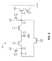
- FIG. 5 is an illustrative schematic of a pixel for reducing high intensity light induced flicker in accordance with an embodiment of the present disclosure.
- FIG. 1 is a block diagram illustrating an example imaging system 100 that detects high intensity illumination without flickering in accordance with an embodiment of the present disclosure.
- Imaging system 100 may be a complementary metal-oxide-semiconductor (“CMOS”) image sensor. As shown in the illustrated embodiment of FIG. 1 , imaging system 100 includes pixel array 102 coupled to control circuitry 108 and readout circuitry 106 , which is coupled to function logic 112 .
- CMOS complementary metal-oxide-semiconductor
- each pixel cell is a CMOS imaging pixel.
- each pixel cell is arranged into a row (e.g., rows R 1 to Ry) and a column (e.g., columns C 1 to Cx) to acquire image data of a person, place or object, etc., which can then be used to render an image of the person, place or object, etc.
- each pixel cell 104 e.g., pixel cells P 1 , P 2 , . . . , Pn
- the image data is read out by readout circuitry 106 through readout column bit lines 110 and then transferred to function logic 112 .
- readout circuitry 106 may include amplification circuitry (not illustrated), a column readout circuit that includes analog-to-digital conversion (ADC) circuitry, or otherwise.
- ADC analog-to-digital conversion
- the read out circuitry 106 may combine image charge provided on the two bit lines 110 and aggregate the image charge into the image data.
- control circuitry 108 is coupled to pixel array 102 to control operational characteristics of pixel array 102 .
- control circuitry 108 may generate a shutter signal for controlling image acquisition.
- the shutter signal is a global shutter signal for simultaneously enabling all pixels within pixel array 102 to simultaneously capture their respective image data during a single acquisition window.
- the shutter signal is a rolling shutter signal such that each row, column, or group of pixels is sequentially enabled during consecutive acquisition windows.
- the shutter signal may also establish an exposure time, which is the length of time that the shutter remains open. In one embodiment, the exposure time is set to be the same for each of the frames.
- the first and second floating diffusions 224 , 226 may be coupled to the first and second source-follower transistors 228 , 232 , respectively, through different mechanisms.
- the first floating diffusion 224 may be directly coupled to a gate terminal of the first source-follower transistor 228
- the second floating diffusion 226 may be capacitively-coupled to a gate of the second source-follower transistor 232 .
- the direct connection may be formed from a metal to semiconductor contact made to the first floating diffusion 224 .
- the capacitor 250 may provide the capacitive coupling between the second floating diffusion 226 and the second source-follower 232 .
- the capacitor 250 may be a metal-oxide-semiconductor capacitor.
- the semiconductor side of the capacitor 250 may be coupled to the second floating diffusion 226
- the metal side of the capacitor 250 may be coupled to the gate of the second source-follower transistor 232 .
- the capacitive coupling of the second floating diffusion 226 to the second source-follower transistor 232 may reduce dark current generation in the second floating diffusion 226 due to a lack of a direct metal connection to the second floating diffusion 226 .
- high intensity illumination from a super bright LED for example, incident on the photodiode 214 may cause the photodiode 214 to generate image charge in an amount greater than a full well capacity, e.g., charge storage capacity, of the photodiode 214 .
- the excess charge may bloom, e.g., transfer, to the second floating diffusion 226 due to a leaky nature of the anti-blooming gate 218 .
- the anti-blooming gate 218 may be leakier than the transfer gate 216 .
- the anti-blooming gate 218 may be biased at its gate so that a channel is formed to allow the excess charge to bloom to the second floating diffusion 226 .
- the charge amount that is within, e.g., less than, the full well capacity of the photodiode 214 may remain in the photodiode 214 till a read out is performed.
- the illumination incident on the photodiode 214 may generate charge that is less than the full well capacity of the photodiode 214 . In such instances, there may be no excess charge to bloom into the second floating diffusion 226 .
- the second source-follower transistor 232 may act like a voltage-controlled resistor and provide a portion of VDD to the second row select transistor 234 . If, for example, the voltage on the capacitor 250 is at a voltage level to induce saturation, the second source-follower transistor 232 may provide VDD to the second row select transistor 234 .
- a readout circuit such as the readout circuitry 106 , may receive voltage representative of the image charge and the excess image charge via bitlines 1 and 2 .
- the readout circuit in response, may aggregate the image charge and the excess image charge to generate image data, which may then be provided to function logic, for example.
- pixel 204 depicts only one photodiode, any number of photodiodes may be coupled to the first and second floating diffusions 224 , 226 . In such embodiments that include multiple photodiodes, each photodiode may be referred to as a subpixel, for example. Additionally, other pixel control functionality may be included in the pixel 204 to assist in operating the pixel in high intensity illumination settings. For example, conversion gain techniques, excess image charge drains, and dual floating diffusion switches, along with other features known to those skilled in the art, may be implemented in the pixel 204 .
- FIG. 3 is an illustrative schematic of a pixel 304 for reducing flickering due to high illumination in accordance with an embodiment of the present disclosure.
- the pixel 304 may be an example of a pixel 104 of pixel array 102 .
- the illustrated embodiment of the pixel 304 includes substantially the same components of the pixel 204 , plus additional photodiodes, transfer gates, and anti-blooming gates.
- the pixel 304 may include a plurality of pixels, or subpixels, all coupled to the first floating diffusion, and some coupled to the second floating diffusion, with each of the plurality of pixels having respective transfer gates and anti-blooming gates.
- the pixel 304 may limit or eliminate image flicker induced by high illumination sources, for example.
- the illustrated embodiment of pixel 304 includes a plurality of photodiodes 314 A-C, a plurality of transfer gates 316 A-C, and a plurality of anti-blooming gates 318 A-C. Additionally, the pixel 304 includes first and second floating diffusions 324 and 326 , first and second reset transistors 320 and 322 , first and second source-follower transistors 328 and 332 , and first and second row select transistors 330 and 334 . The plurality of photodiodes 314 A-C may be coupled to the first floating diffusion 324 through a respective one of the plurality of transfer gates 316 A-C.
- a subset of the plurality of photodiodes 314 A-C may be coupled to the second floating diffusion 326 through respective ones of the plurality of anti-blooming gates 318 A-C.
- Remaining ones of the plurality of photodiodes may be coupled to an anti-blooming (AB) drain, e.g., a voltage reference source, via a respective anti-blooming gate 318 .
- AB anti-blooming
- the photodiode 314 C is coupled to the AB drain via the anti-blooming gate 318 C
- the photodiodes 314 A, B are coupled to the second floating diffusion 326 via their respective anti-blooming gates 318 A, B.
- the anti-blooming gates 318 A-C may be leakier than their associated transfer gates 316 A-C, else they may be biased to be leakier than their associated transfer gates 316 A-C. By making the anti-blooming gates 318 A-C leakier than their associated transfer gates 316 A-C, charge generated in excess of the full well capacity of their associated photodiode 314 A-C may bloom into the second floating diffusion 326 and/or the AB drain.
- the second floating diffusion 326 and the second source-follower 332 may be capacitively coupled by the capacitor 350 .
- the capacitor 350 which may be a MOS capacitor, may negate the need to provide a direct electrical connection between the gate of the second source-follower 332 and the second floating diffusion 326 . Omitting the direct connection between the two may reduce or eliminate dark current generation within the second floating diffusion 326 . While the second floating diffusion 326 and the second source-follower 332 are capacitively coupled, the first floating diffusion 324 and the first source-follower 328 may be directly coupled via a metal to semiconductor contact.
- the first and second reset transistors 320 , 322 may be coupled to reset a voltage of their respective floating diffusions 324 , 326 under control of a reset signal received at gates of the first and second reset transistors 320 , 322 .
- the reset transistors 320 , 322 may discharge or charge the respective first and second floating diffusions 324 , 326 to a preset voltage, which may be performed before the integration of image light incident on the photodiodes 314 A-C.
- the first and second floating diffusions 324 , 326 may be coupled to gates of the first and second source-follower transistors 328 , 332 , respectively.
- the first and second source-follower transistors 328 , 332 operate as source-followers providing a high impedance output from the associated first and second floating diffusions 324 , 326 .
- the first and second row select transistors 330 , 334 may selectively couple the output of the pixel circuitry in the pixel 304 to the column bitlines 1 and 2 under control of a received row select signal.
- the first and second reset transistors 320 , 322 , and the first and second source-follower transistors may be coupled to shared reference voltages, such as VDD.
- the photodiodes 314 A-C may be illuminated to photogenerate image charge.
- the illumination source is a low light intensity source
- the photodiodes 314 A-C may generate image charge that is equal to or less than their respective full well capacities, e.g., charge storage capacities.
- the illumination source is a high intensity source, such as an LED
- the photodiodes 314 A-C may generate image charge in excess of their respective full well capacities. As such, the excess image charge may either bloom to the second floating diffusion 326 , or to the AB drain, depending on the coupling.
- the excess charge generated in photodiodes 314 A, B may bloom, e.g., transfer, to the second floating diffusion 326 , whereas excess charge generated by the photodiode 314 C may bloom to the AB drain.
- Charge bloomed to the AB drain may not contribute to image data, for example.
- the excess charge may bloom due to the anti-blooming gates 318 A-C being leaky, either due to fabrication or biasing.
- the charge remaining in the photodiodes 314 A, B may be read out onto bitline 1 using the four transistor (4T) timing.
- 4T the excess charge on the second floating diffusion 326
- three transistor (3T) timing may be used to read the charge out onto bitline 2 .
- the excess charge on the second floating diffusion 326 may cause a voltage to build up on the capacitor 350 .
- the voltage on the capacitor 350 may enable the second source-follower transistor 332 .
- the second source-follower transistor 332 may be enabled into various operating conditions, such as ohmic or saturation.
- the second source-follower transistor 332 may act like a voltage-controlled resistor and provide a portion of VDD to the second row select transistor 334 . If, for example, the voltage on the capacitor 350 is at a voltage level to induce saturation, the second source-follower transistor 332 may provide VDD to the second row select transistor 334 .
- a readout circuit such as the readout circuitry 106 , may receive voltage representative of the image charge and the excess image charge via bitlines 1 and 2 .
- the readout circuit in response, may aggregate the image charge and the excess image charge to generate image data, which may then be provided to function logic, for example.
- FIG. 4 is an illustrative schematic of a pixel 404 for reducing flickering due to high illumination in accordance with an embodiment of the present disclosure.
- the pixel 404 may be an example of a pixel 104 of pixel array 102 .
- the illustrated embodiment of the pixel 404 includes substantially similar components of the pixel 204 or pixel 304 , plus first and second dual conversion gain (DCG) gates (DCG 1 and DCG 2 ) 436 and 438 , and first and second DCG capacitors (C DCG1 and C DCG2 ) 440 and 442 .
- DCG dual conversion gain
- the pixel 404 is shown to include only a single photodiode, a plurality of photodiodes, similar for instance to the pixel 304 , all coupled to the first floating diffusion, and some coupled to the second floating diffusion, with each of the plurality of pixels having respective transfer gates and anti-blooming gates may be included in the pixel 404 .
- the pixel 404 may limit or eliminate image flicker induced by high illumination sources, for example.
- the second floating diffusion 426 and the second source-follower 432 may be capacitively coupled by the capacitor 450 , which may be a MOS capacitor.
- the second floating diffusion 426 may be coupled to the semiconductor side of the capacitor 450
- the gate of the second source-follower transistor 432 may be coupled to the metal side of the capacitor 450 .
- the first and second DCG gates 436 , 438 may be coupled between the first and second floating diffusions 424 , 426 , respectively, and the first and second DCG capacitors 440 , 442 , respectively.
- the first and second DCG gates 436 , 438 may be coupled to selectively adjust a conversion gain of the first and second floating diffusions 424 , 426 in response to receiving a DCG signal on their respective gates. For example, in response to receiving a DCG signal, either or both of the DCG gates 436 , 438 may couple their respective floating diffusions 424 , 426 to the DCG capacitors 440 , 442 .
- the conversion gains of the respective floating diffusions 424 , 426 may be reduced, for example, due to the DCG capacitors 440 , 442 , which are coupled to ground, absorbing charge from the first and second floating diffusions 424 , 426 , respectively.
- the DCG capacitors 440 , 442 may be selectively coupled to the first and second floating diffusions 424 , 426 to increase their respective conversion gains.
- the DCG signal may be provided by control circuitry, such as the control circuitry 108 for example.
- the photodiode 414 may be illuminated to photogenerate image charge.
- the illumination source is a low light intensity source
- the photodiode 414 may generate image charge that is equal to or less than its full well capacity, e.g., charge storage capacity.
- the illumination source is a high intensity source, such as an LED
- the photodiode 414 may generate image charge in excess of the full well capacity. As such, the excess image charge may bloom to the second floating diffusion 426 .
- the excess charge may bloom due to the anti-blooming gate 418 being leaky, either due to fabrication or biasing.
- the charge remaining in the photodiode 414 may be read out onto bitline 1 using the four transistor (4T) timing or dual conversion gain.
- 4T four transistor
- either three transistor (3T) timing or dual conversion gain may be used to read the charge out onto bitline 2 .
- the second floating diffusion 526 and the second source-follower 532 may be capacitively coupled by the capacitor 550 , which may be a MOS capacitor.
- the second floating diffusion 526 may be coupled to the semiconductor side of the capacitor 550
- the gate of the second source-follower transistor 532 may be coupled to the metal side of the capacitor 550 .
- the photodiode 514 may be illuminated to photogenerate image charge.
- the illumination source is a low light intensity source
- the photodiode 514 may generate image charge that is equal to or less than its full well capacity.
- the illumination source is a high intensity source, such as an LED
- the photodiode 514 may generate image charge in excess of the full well capacity. As such, the excess image charge may bloom to the second floating diffusion 526 .
- the excess charge may bloom due to the anti-blooming gate 518 being leaky, either due to fabrication or biasing.
- pixel 504 is depicted as having a single photodiode, multiple photodiodes may be included in the pixel 504 , which may be coupled to the first and second floating diffusions 524 , 526 similar to the pixel 304 .
Landscapes
- Engineering & Computer Science (AREA)
- Multimedia (AREA)
- Signal Processing (AREA)
- Transforming Light Signals Into Electric Signals (AREA)
- Solid State Image Pick-Up Elements (AREA)
Abstract
Description
- This disclosure relates generally to image sensors, and in particular but not exclusively, relates to image sensors having pixels for detection of high intensity light sources without the inducement of flicker by the image sensor.
- High-speed image sensors have been widely used in many applications in different fields including the automotive field, the machine vision field, and the field of professional video photography. Some applications in these fields require the detection and capture of LED lights, which has proven to be difficult. For example, automotive image sensors face the problem of LED flickering. Future automotive vehicle lights, traffic lights and signs will include LED that is pulsed at 90-300 Hz with high peak light intensity. This requires that the minimum exposure time be kept over 10 ms. A very high full well capacity or very low light intensity are thus needed to avoid pixels to get saturated and lose useful information.
- Current solutions to address the overflow and loss of useful information from saturated pixels include enhancing the full well capacity with a lateral overflow integrating capacitor (LOFIC). When the photodiode is filled after reaching a corresponding FWC, the excess charge is leaked into a floating drain. A large capacitor connected to the floating drain can then store the excess charge. However, the maximum full well capacity is thus limited by the floating drain capacitor rather than the photodiode full well capacity. Other solutions involve using non-linear sensor (e.g., logarithmic sensors) to enlarge the full well capacity, or using split diode pixels or subpixel sensors to maintain minimum exposure time by minimizing sensitivity of small photodiode.
- Non-limiting and non-exhaustive examples of the invention are described with reference to the following figures, wherein like reference numerals refer to like parts throughout the various views unless otherwise specified.
-
FIG. 1 is a block diagram illustrating an example imaging system that detects high intensity illumination without flickering in accordance with an embodiment of the present disclosure. -
FIG. 2 is an illustrative schematic of a pixel for reducing flickering due to high illumination in accordance with an embodiment of the present disclosure. -
FIG. 3 is an illustrative schematic of a pixel for reducing flickering due to high illumination in accordance with an embodiment of the present disclosure. -
FIG. 4 is an illustrative schematic of a pixel for reducing flickering due to high illumination in accordance with an embodiment of the present disclosure. -
FIG. 5 is an illustrative schematic of a pixel for reducing high intensity light induced flicker in accordance with an embodiment of the present disclosure. - Corresponding reference characters indicate corresponding components throughout the several views of the drawings. Skilled artisans will appreciate that elements in the figures are illustrated for simplicity and clarity and have not necessarily been drawn to scale. For example, the dimensions of some of the elements in the figures may be exaggerated relative to other elements to help to improve understanding of various embodiments of the present invention. Also, common but well-understood elements that are useful or necessary in a commercially feasible embodiment are often not depicted in order to facilitate a less obstructed view of these various embodiments of the present invention.
- Examples of an apparatus and method for an image sensor with pixels that reduce or eliminate flicker induced by high intensity illumination are described herein. In the following description, numerous specific details are set forth to provide a thorough understanding of the examples. One skilled in the relevant art will recognize; however, that the techniques described herein can be practiced without one or more of the specific details, or with other methods, components, materials, etc. In other instances, well-known structures, materials, or operations are not shown or described in detail to avoid obscuring certain aspects.
- Reference throughout this specification to “one example” or “one embodiment” means that a particular feature, structure, or characteristic described in connection with the example is included in at least one example of the present invention. Thus, the appearances of the phrases “in one example” or “in one embodiment” in various places throughout this specification are not necessarily all referring to the same example. Furthermore, the particular features, structures, or characteristics may be combined in any suitable manner in one or more examples.
- Throughout this specification, several terms of art are used. These terms are to take on their ordinary meaning in the art from which they come, unless specifically defined herein or the context of their use would clearly suggest otherwise. It should be noted that element names and symbols may be used interchangeably through this document (e.g., Si vs. silicon); however, both have identical meaning.
-
FIG. 1 is a block diagram illustrating anexample imaging system 100 that detects high intensity illumination without flickering in accordance with an embodiment of the present disclosure.Imaging system 100 may be a complementary metal-oxide-semiconductor (“CMOS”) image sensor. As shown in the illustrated embodiment ofFIG. 1 ,imaging system 100 includespixel array 102 coupled tocontrol circuitry 108 andreadout circuitry 106, which is coupled tofunction logic 112. - The illustrated embodiment of
pixel array 102 is a two-dimensional (“2D”) array of imaging sensors or pixel cells 104 (e.g., pixel cells P1, P2, . . . , Pn). In one example, each pixel cell is a CMOS imaging pixel. As illustrated, each pixel cell is arranged into a row (e.g., rows R1 to Ry) and a column (e.g., columns C1 to Cx) to acquire image data of a person, place or object, etc., which can then be used to render an image of the person, place or object, etc. In some embodiments, each pixel cell 104 (e.g., pixel cells P1, P2, . . . , Pn) may include a plurality of subpixels respectively including a plurality of photodiodes and a plurality of associated transfer gate transistors and anti-blooming gate transistors. - In one example, after each pixel has acquired its image data or image charge, the image data is read out by
readout circuitry 106 through readoutcolumn bit lines 110 and then transferred tofunction logic 112. In some embodiments, there may be twobit lines 110 per pixel. In various examples,readout circuitry 106 may include amplification circuitry (not illustrated), a column readout circuit that includes analog-to-digital conversion (ADC) circuitry, or otherwise. In embodiments having twobit lines 110 per pixel, the read outcircuitry 106 may combine image charge provided on the twobit lines 110 and aggregate the image charge into the image data.Function logic 112 may simply store the image data or even manipulate the image data by applying post image effects (e.g., crop, rotate, remove red eye, adjust brightness, adjust contrast, or otherwise). In one example,readout circuitry 106 may read out a row of image data at a time along readout column lines (illustrated) or may read out the image data using a variety of other techniques (not illustrated), such as a serial read out or a full parallel read out of all pixels simultaneously. - In one example,
control circuitry 108 is coupled topixel array 102 to control operational characteristics ofpixel array 102. For example,control circuitry 108 may generate a shutter signal for controlling image acquisition. In one example, the shutter signal is a global shutter signal for simultaneously enabling all pixels withinpixel array 102 to simultaneously capture their respective image data during a single acquisition window. In another example, the shutter signal is a rolling shutter signal such that each row, column, or group of pixels is sequentially enabled during consecutive acquisition windows. The shutter signal may also establish an exposure time, which is the length of time that the shutter remains open. In one embodiment, the exposure time is set to be the same for each of the frames. - In another example,
control circuitry 108 may comprise the horizontal and vertical scanning circuitry, which selects the row and/or column of pixels to be read out. Scanning circuitry may include, selection circuitry (e.g., multiplexers), etc. to readout a row or column of image data at a time along readout column bit lines 109 or may readout the image data using a variety of other techniques, such as a serial readout or a full parallel readout of all pixels simultaneously. When scanning circuitry selectspixels 104 inpixel array 102, the pixels convert light incident to the pixels to a signal and output the signal tocolumn readout circuitry 106.Column readout circuitry 106 may receive the signal from scanning circuitry or frompixel array 102. -
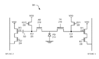
FIG. 2 is an illustrative schematic of apixel 204 for reducing flickering due to high illumination in accordance with an embodiment of the present disclosure. Thepixel 204 may be an example of apixel 104 ofpixel array 102. The illustrated embodiment of thepixel 204 includes a photodiode (PD) 214, a transfer gate (TX) 216, an anti-blooming gate (AB) 218, first and second reset transistors (RST1 and RST2) 220 and 222, first and second floating diffusions (FD1 and FD2) 224 and 226, first and second source-follower transistors (SF1 and SF2) 228 and 232, and first and second row selection transistors (RS1 and RS2) 230 and 234. Thepixel 204 may be exposed to image light during an integration and generate image charge in response. When a source of the image charge is a high illumination source, which may be a point source at times, such as a light emitting diode (LED), the charge generated by thephotodiode 214 may be greater than a full well capacity of thephotodiode 214. During such instances, the excess charge, e.g., the charge generated that is greater than the full well capacity of thephotodiode 214, may bloom into the second floating diffusion due to the leaky nature of theanti-blooming gate 218. - The first and second floating
diffusions follower transistors diffusion 224 may be directly coupled to a gate terminal of the first source-follower transistor 228, while the second floatingdiffusion 226 may be capacitively-coupled to a gate of the second source-follower transistor 232. The direct connection may be formed from a metal to semiconductor contact made to the first floatingdiffusion 224. Thecapacitor 250 may provide the capacitive coupling between the second floatingdiffusion 226 and the second source-follower 232. - In some embodiments, the
capacitor 250 may be a metal-oxide-semiconductor capacitor. In such an embodiment, the semiconductor side of thecapacitor 250 may be coupled to the second floatingdiffusion 226, and the metal side of thecapacitor 250 may be coupled to the gate of the second source-follower transistor 232. The capacitive coupling of the second floatingdiffusion 226 to the second source-follower transistor 232 may reduce dark current generation in the second floatingdiffusion 226 due to a lack of a direct metal connection to the second floatingdiffusion 226. - The first and
second reset transistors diffusions diffusions second reset transistors diffusions follower transistors follower transistors diffusions select transistors pixel 204 to the column bitlines 1 and 2 under control of a received row select signal. - Also included in the
pixel 204 are a shared source-follower voltage supply connection VDD, column bitline connections, and a shared reset voltage supply connection VDD. - During signal integration, high intensity illumination, from a super bright LED for example, incident on the
photodiode 214 may cause thephotodiode 214 to generate image charge in an amount greater than a full well capacity, e.g., charge storage capacity, of thephotodiode 214. The excess charge may bloom, e.g., transfer, to the second floatingdiffusion 226 due to a leaky nature of theanti-blooming gate 218. In general, theanti-blooming gate 218 may be leakier than thetransfer gate 216. In some embodiments, theanti-blooming gate 218 may be biased at its gate so that a channel is formed to allow the excess charge to bloom to the second floatingdiffusion 226. The charge amount that is within, e.g., less than, the full well capacity of thephotodiode 214 may remain in thephotodiode 214 till a read out is performed. - In some instances, the illumination incident on the
photodiode 214 may generate charge that is less than the full well capacity of thephotodiode 214. In such instances, there may be no excess charge to bloom into the second floatingdiffusion 226. - During read out after a high intensity illumination event, the charge remaining in the
photodiode 214 may be read out onbitline 1 using a four transistor (4T) timing. To read out the excess charge on the second floatingdiffusion 226, three transistor (3T) timing may be used to read the charge out onbitline 2. The excess charge on the second floatingdiffusion 226 may cause a voltage to build up on thecapacitor 250. In turn, the voltage on thecapacitor 250 may enable the second source-follower transistor 232. Depending on the voltage on thecapacitor 250, the second source-follower transistor 232 may be enabled into various operating conditions, such as ohmic or saturation. If, for example, the voltage on thecapacitor 250 is at a voltage level to induce ohmic operation, the second source-follower transistor 232 may act like a voltage-controlled resistor and provide a portion of VDD to the second rowselect transistor 234. If, for example, the voltage on thecapacitor 250 is at a voltage level to induce saturation, the second source-follower transistor 232 may provide VDD to the second rowselect transistor 234. - During readout, a readout circuit, such as the
readout circuitry 106, may receive voltage representative of the image charge and the excess image charge viabitlines - While the illustrated embodiment of
pixel 204 depicts only one photodiode, any number of photodiodes may be coupled to the first and second floatingdiffusions pixel 204 to assist in operating the pixel in high intensity illumination settings. For example, conversion gain techniques, excess image charge drains, and dual floating diffusion switches, along with other features known to those skilled in the art, may be implemented in thepixel 204. -
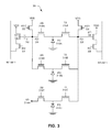
FIG. 3 is an illustrative schematic of apixel 304 for reducing flickering due to high illumination in accordance with an embodiment of the present disclosure. Thepixel 304 may be an example of apixel 104 ofpixel array 102. The illustrated embodiment of thepixel 304 includes substantially the same components of thepixel 204, plus additional photodiodes, transfer gates, and anti-blooming gates. In general, thepixel 304 may include a plurality of pixels, or subpixels, all coupled to the first floating diffusion, and some coupled to the second floating diffusion, with each of the plurality of pixels having respective transfer gates and anti-blooming gates. Thepixel 304 may limit or eliminate image flicker induced by high illumination sources, for example. - The illustrated embodiment of
pixel 304 includes a plurality ofphotodiodes 314A-C, a plurality oftransfer gates 316A-C, and a plurality ofanti-blooming gates 318A-C. Additionally, thepixel 304 includes first and second floatingdiffusions second reset transistors follower transistors select transistors photodiodes 314A-C may be coupled to the first floatingdiffusion 324 through a respective one of the plurality oftransfer gates 316A-C. Further, a subset of the plurality ofphotodiodes 314A-C may be coupled to the second floatingdiffusion 326 through respective ones of the plurality ofanti-blooming gates 318A-C. Remaining ones of the plurality of photodiodes may be coupled to an anti-blooming (AB) drain, e.g., a voltage reference source, via a respective anti-blooming gate 318. For example, in the embodiment ofFIG. 3 , thephotodiode 314C is coupled to the AB drain via the anti-blooming gate 318C, while thephotodiodes 314A, B are coupled to the second floatingdiffusion 326 via their respectiveanti-blooming gates 318A, B. - The
anti-blooming gates 318A-C may be leakier than their associatedtransfer gates 316A-C, else they may be biased to be leakier than their associatedtransfer gates 316A-C. By making theanti-blooming gates 318A-C leakier than their associatedtransfer gates 316A-C, charge generated in excess of the full well capacity of their associatedphotodiode 314A-C may bloom into the second floatingdiffusion 326 and/or the AB drain. - The second floating
diffusion 326 and the second source-follower 332 may be capacitively coupled by thecapacitor 350. Thecapacitor 350, which may be a MOS capacitor, may negate the need to provide a direct electrical connection between the gate of the second source-follower 332 and the second floatingdiffusion 326. Omitting the direct connection between the two may reduce or eliminate dark current generation within the second floatingdiffusion 326. While the second floatingdiffusion 326 and the second source-follower 332 are capacitively coupled, the first floatingdiffusion 324 and the first source-follower 328 may be directly coupled via a metal to semiconductor contact. - The first and
second reset transistors diffusions second reset transistors reset transistors diffusions photodiodes 314A-C. The first and second floatingdiffusions follower transistors follower transistors diffusions select transistors pixel 304 to the column bitlines 1 and 2 under control of a received row select signal. The first andsecond reset transistors - During signal integration, the
photodiodes 314A-C may be illuminated to photogenerate image charge. When, for example, the illumination source is a low light intensity source, thephotodiodes 314A-C may generate image charge that is equal to or less than their respective full well capacities, e.g., charge storage capacities. However, when, for example, the illumination source is a high intensity source, such as an LED, thephotodiodes 314A-C may generate image charge in excess of their respective full well capacities. As such, the excess image charge may either bloom to the second floatingdiffusion 326, or to the AB drain, depending on the coupling. For example, the excess charge generated inphotodiodes 314A, B may bloom, e.g., transfer, to the second floatingdiffusion 326, whereas excess charge generated by thephotodiode 314C may bloom to the AB drain. Charge bloomed to the AB drain may not contribute to image data, for example. The excess charge may bloom due to theanti-blooming gates 318A-C being leaky, either due to fabrication or biasing. - During read out post a high intensity illumination event, the charge remaining in the
photodiodes 314A, B may be read out ontobitline 1 using the four transistor (4T) timing. To read out the excess charge on the second floatingdiffusion 326, three transistor (3T) timing may be used to read the charge out ontobitline 2. The excess charge on the second floatingdiffusion 326 may cause a voltage to build up on thecapacitor 350. In turn, the voltage on thecapacitor 350 may enable the second source-follower transistor 332. Depending on the voltage on thecapacitor 350, the second source-follower transistor 332 may be enabled into various operating conditions, such as ohmic or saturation. If, for example, the voltage on thecapacitor 350 is at a voltage level to induce ohmic operation, the second source-follower transistor 332 may act like a voltage-controlled resistor and provide a portion of VDD to the second rowselect transistor 334. If, for example, the voltage on thecapacitor 350 is at a voltage level to induce saturation, the second source-follower transistor 332 may provide VDD to the second rowselect transistor 334. - During readout, a readout circuit, such as the
readout circuitry 106, may receive voltage representative of the image charge and the excess image charge viabitlines -
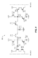
FIG. 4 is an illustrative schematic of apixel 404 for reducing flickering due to high illumination in accordance with an embodiment of the present disclosure. Thepixel 404 may be an example of apixel 104 ofpixel array 102. The illustrated embodiment of thepixel 404 includes substantially similar components of thepixel 204 orpixel 304, plus first and second dual conversion gain (DCG) gates (DCG1 and DCG2) 436 and 438, and first and second DCG capacitors (CDCG1 and CDCG2) 440 and 442. While thepixel 404 is shown to include only a single photodiode, a plurality of photodiodes, similar for instance to thepixel 304, all coupled to the first floating diffusion, and some coupled to the second floating diffusion, with each of the plurality of pixels having respective transfer gates and anti-blooming gates may be included in thepixel 404. Thepixel 404 may limit or eliminate image flicker induced by high illumination sources, for example. - For sake of brevity, features of the
pixel 404 that have been discussed with respect topixel 204 and/or pixel 403 ofFIGS. 2 and/or 3 will be omitted from the discussion ofpixel 404. For example, the second floatingdiffusion 426 and the second source-follower 432 may be capacitively coupled by thecapacitor 450, which may be a MOS capacitor. As such, the second floatingdiffusion 426 may be coupled to the semiconductor side of thecapacitor 450, while the gate of the second source-follower transistor 432 may be coupled to the metal side of thecapacitor 450. - The first and
second DCG gates diffusions second DCG capacitors second DCG gates diffusions DCG gates diffusions DCG capacitors DCG capacitors diffusions diffusions DCG capacitors diffusions DCG capacitors diffusions control circuitry 108 for example. - During signal integration, the
photodiode 414 may be illuminated to photogenerate image charge. When, for example, the illumination source is a low light intensity source, thephotodiode 414 may generate image charge that is equal to or less than its full well capacity, e.g., charge storage capacity. However, when, for example, the illumination source is a high intensity source, such as an LED, thephotodiode 414 may generate image charge in excess of the full well capacity. As such, the excess image charge may bloom to the second floatingdiffusion 426. The excess charge may bloom due to theanti-blooming gate 418 being leaky, either due to fabrication or biasing. - During read out post a high intensity illumination event, the charge remaining in the
photodiode 414 may be read out ontobitline 1 using the four transistor (4T) timing or dual conversion gain. To read out the excess charge on the second floatingdiffusion 426, either three transistor (3T) timing or dual conversion gain may be used to read the charge out ontobitline 2. - During readout, a readout circuit, such as the
readout circuitry 106, may receive voltage representative of the image charge and the excess image charge viabitlines - While
pixel 404 is depicted as having two DCG gates and capacitors,pixel 404 may include only a single DCG gate and capacitor in some embodiments. For example, a single DCG gate and DCG capacitor may be coupled between ground and the first floatingdiffusion 424. Additionally, multiple photodiodes may be included in thepixel 404, which may be coupled to the first and second floatingdiffusions pixel 304. -
FIG. 5 is an illustrative schematic of apixel 504 for reducing high intensity light induced flicker in accordance with an embodiment of the present disclosure. Thepixel 504 may be an example of thepixel 104. The illustrated embodiment of thepixel 504 includes many of the same components of thepixels pixel 504 may be coupled to a single bitline, instead of multiple bitlines. Additionally, thepixel 504 includes the dual floating diffusion (DFD)transistor 544. Thepixel 504 may limit or eliminate image flicker induced by high illumination sources, for example. - For sake of brevity, features of the
pixel 504 that have been discussed with respect topixels FIGS. 2, 3 and/or 4 will be omitted from the discussion ofpixel 504. For example, the second floatingdiffusion 526 and the second source-follower 532 may be capacitively coupled by thecapacitor 550, which may be a MOS capacitor. As such, the second floatingdiffusion 526 may be coupled to the semiconductor side of thecapacitor 550, while the gate of the second source-follower transistor 532 may be coupled to the metal side of thecapacitor 550. - The
capacitor 550 may be coupled to theDFD transistor 544, which may also be coupled to the first floatingdiffusion 524. Thecapacitor 550 may additionally be coupled to the second floatingdiffusion 526. TheDFD transistor 544 may selectively couple thecapacitor 550 to the first floatingdiffusion 524 in response to a DFD signal received, for example, from control circuitry. Example control circuitry may be thecontrol circuitry 108 of theimaging system 100. - During signal integration, the
photodiode 514 may be illuminated to photogenerate image charge. When, for example, the illumination source is a low light intensity source, thephotodiode 514 may generate image charge that is equal to or less than its full well capacity. However, when, for example, the illumination source is a high intensity source, such as an LED, thephotodiode 514 may generate image charge in excess of the full well capacity. As such, the excess image charge may bloom to the second floatingdiffusion 526. The excess charge may bloom due to theanti-blooming gate 518 being leaky, either due to fabrication or biasing. - During read out post a high intensity illumination event, the charge remaining in the
photodiode 514 may be read out onto the bitline using the four transistor (4T) timing. To read out the excess charge on the second floatingdiffusion 526, three transistor (3T) timing in combination with enabling theDFD transistor 544 may be used to read the charge out onto the bitline via the first floatingdiffusion 524. - During readout, a readout circuit, such as the
readout circuitry 106, may receive voltage representative of the image charge and the excess image charge viabitlines - While
pixel 504 is depicted as having a single photodiode, multiple photodiodes may be included in thepixel 504, which may be coupled to the first and second floatingdiffusions pixel 304. - The above description of illustrated examples of the invention, including what is described in the Abstract, is not intended to be exhaustive or to limit the invention to the precise forms disclosed. While specific examples of the invention are described herein for illustrative purposes, various modifications are possible within the scope of the invention, as those skilled in the relevant art will recognize.
- These modifications can be made to the invention in light of the above detailed description. The terms used in the following claims should not be construed to limit the invention to the specific examples disclosed in the specification. Rather, the scope of the invention is to be determined entirely by the following claims, which are to be construed in accordance with established doctrines of claim interpretation.
Claims (20)
Priority Applications (3)
| Application Number | Priority Date | Filing Date | Title |
|---|---|---|---|
| US15/285,352 US9936153B1 (en) | 2016-10-04 | 2016-10-04 | CMOS image sensor with dual floating diffusions per pixel for flicker-free detection of light emitting diodes |
| CN201710905557.3A CN107895729B (en) | 2016-10-04 | 2017-09-29 | Image sensor pixel and imaging system with reduced illumination-induced flicker |
| TW106134117A TWI661544B (en) | 2016-10-04 | 2017-10-03 | Cmos image sensor with dual floating diffusions per pixel for flicker-free detection of light emitting diodes |
Applications Claiming Priority (1)
| Application Number | Priority Date | Filing Date | Title |
|---|---|---|---|
| US15/285,352 US9936153B1 (en) | 2016-10-04 | 2016-10-04 | CMOS image sensor with dual floating diffusions per pixel for flicker-free detection of light emitting diodes |
Publications (2)
| Publication Number | Publication Date |
|---|---|
| US9936153B1 US9936153B1 (en) | 2018-04-03 |
| US20180098008A1 true US20180098008A1 (en) | 2018-04-05 |
Family
ID=61711691
Family Applications (1)
| Application Number | Title | Priority Date | Filing Date |
|---|---|---|---|
| US15/285,352 Active US9936153B1 (en) | 2016-10-04 | 2016-10-04 | CMOS image sensor with dual floating diffusions per pixel for flicker-free detection of light emitting diodes |
Country Status (3)
| Country | Link |
|---|---|
| US (1) | US9936153B1 (en) |
| CN (1) | CN107895729B (en) |
| TW (1) | TWI661544B (en) |
Cited By (7)
| Publication number | Priority date | Publication date | Assignee | Title |
|---|---|---|---|---|
| CN109889735A (en) * | 2019-04-22 | 2019-06-14 | Oppo广东移动通信有限公司 | Pixel circuit and image sensor |
| US20200068156A1 (en) * | 2018-08-22 | 2020-02-27 | Gigajot Technology Inc. | Split-readout image sensor |
| US20210025993A1 (en) * | 2019-07-25 | 2021-01-28 | Omnivision Technologies, Inc. | Tri-gate charge transfer block structure in time of flight pixel |
| CN112788258A (en) * | 2019-11-05 | 2021-05-11 | 豪威科技股份有限公司 | Multi-element pixel array for high dynamic range image sensor |
| US11450696B1 (en) * | 2021-04-13 | 2022-09-20 | Omnivision Technologies, Inc. | Dual floating diffusion transistor with vertical gate structure for image sensor |
| US20220303487A1 (en) * | 2018-08-22 | 2022-09-22 | Gigajot Technology, Inc. | Split-readout image sensor |
| US20250159373A1 (en) * | 2023-11-13 | 2025-05-15 | Omnivision Technologies, Inc. | Image Sensor and Optical Signal Generation Method |
Families Citing this family (29)
| Publication number | Priority date | Publication date | Assignee | Title |
|---|---|---|---|---|
| JP5985136B2 (en) | 2009-03-19 | 2016-09-06 | ソニー株式会社 | SEMICONDUCTOR DEVICE, ITS MANUFACTURING METHOD, AND ELECTRONIC DEVICE |
| JP6789678B2 (en) * | 2016-06-06 | 2020-11-25 | キヤノン株式会社 | Imaging device, imaging system |
| US10362255B2 (en) * | 2017-02-09 | 2019-07-23 | Semiconductor Components Industries, Llc | Multi-conversion gain pixel configurations |
| US10986290B2 (en) | 2018-05-18 | 2021-04-20 | Omnivision Technologies, Inc. | Wide dynamic range image sensor with global shutter |
| US10623655B2 (en) * | 2018-05-30 | 2020-04-14 | Semiconductor Components Industries, Llc | Image sensors with light flicker mitigation capabilities |
| US10917596B2 (en) * | 2018-08-29 | 2021-02-09 | Himax Imaging Limited | Pixel circuit for generating output signals in response to incident radiation |
| KR20200118723A (en) | 2019-04-08 | 2020-10-16 | 삼성전자주식회사 | Image sensor comprising pixel groups and electronic device including thereof |
| KR20200143559A (en) * | 2019-06-13 | 2020-12-24 | 삼성전자주식회사 | Depth sensor comprising hybrid pixel |
| TWI882059B (en) * | 2020-01-29 | 2025-05-01 | 日商索尼半導體解決方案公司 | Imaging element, imaging device, and ranging device |
| US11658202B2 (en) * | 2020-05-15 | 2023-05-23 | Omnivision Technologies, Inc. | Dual row select pixel for fast pixel binning |
| TWI777573B (en) * | 2020-05-22 | 2022-09-11 | 新加坡商普里露尼庫斯新加坡私人有限公司 | System, method, device and data structure for digital pixel sensors |
| US11812176B2 (en) | 2020-09-01 | 2023-11-07 | Pixart Imaging Inc. | Pixel circuit selecting to output time difference data or image data |
| US11290671B2 (en) | 2020-09-01 | 2022-03-29 | Pixart Imaging Inc. | Pixel circuit outputting pulse width signals and performing analog operation |
| US12347181B2 (en) | 2020-06-05 | 2025-07-01 | Pixart Imaging Inc. | Neural signal detection circuit outputting time difference data or neural data |
| US11706542B2 (en) * | 2020-09-01 | 2023-07-18 | Pixart Imaging Inc. | Pixel circuit outputting time difference data and image data, and operating method of pixel array |
| KR102878956B1 (en) * | 2020-09-03 | 2025-10-30 | 에스케이하이닉스 주식회사 | image sensing device |
| US11399150B2 (en) * | 2020-11-13 | 2022-07-26 | Omnivision Technologies, Inc. | Auto-zero techniques for lateral overflow integrating capacitor (LOFIC) readout image sensor |
| US11463648B1 (en) * | 2021-06-08 | 2022-10-04 | Omnivision Technologies, Inc. | Image sensor with three readout approach for phase detection autofocus and image sensing photodiodes through multiple column bitlines |
| CN114189638B (en) * | 2021-12-03 | 2024-09-13 | 二十一世纪(北京)微电子技术有限公司 | Line scanning circuit of rolling shutter, image sensor and electronic equipment |
| CN116367006A (en) * | 2021-12-17 | 2023-06-30 | 上海集成电路装备材料产业创新中心有限公司 | Pixel unit and image sensor |
| US11830894B2 (en) * | 2021-12-27 | 2023-11-28 | Omnivision Technologies, Inc. | CMOS image sensor pixel for high dynamic range capturing |
| CN116980738B (en) | 2022-04-14 | 2026-04-14 | 思特威(上海)电子科技股份有限公司 | Image sensor pixel, pixel circuit, image sensor and control method |
| CN114928702B (en) * | 2022-05-07 | 2025-10-17 | 中国电子科技集团公司第十三研究所 | Image sensor pixel structure, image sensor and electronic equipment |
| CN114975498A (en) * | 2022-05-09 | 2022-08-30 | 长春长光辰芯光电技术有限公司 | Size-expandable CMOS image sensor pixel and electronic equipment |
| CN114900687B (en) * | 2022-05-17 | 2024-03-05 | 中国科学院新疆理化技术研究所 | A simulation method for the impact of different light intensities on the full well capacity of CMOS image sensor pixel units |
| US11729526B1 (en) * | 2022-06-24 | 2023-08-15 | Omnivision Technologies Inc. | High dynamic range CMOS image sensor pixel with reduced metal-insulator-metal lateral overflow integration capacitor reset settling |
| US12185000B2 (en) * | 2022-07-06 | 2024-12-31 | Omnivision Technologies, Inc. | Pixel circuit for high dynamic range image sensor |
| US11843884B1 (en) * | 2023-04-28 | 2023-12-12 | Omnivision Technologies, Inc. | HV driver for rolling clamp in image sensor |
| US20250254440A1 (en) * | 2024-02-02 | 2025-08-07 | Apple Inc. | High Dynamic Range Image Sensor with Dual-Carrier Pixel Architecture |
Family Cites Families (7)
| Publication number | Priority date | Publication date | Assignee | Title |
|---|---|---|---|---|
| US7286174B1 (en) | 2001-06-05 | 2007-10-23 | Dalsa, Inc. | Dual storage node pixel for CMOS sensor |
| US8184191B2 (en) * | 2006-08-09 | 2012-05-22 | Tohoku University | Optical sensor and solid-state imaging device |
| JP5178364B2 (en) * | 2007-09-06 | 2013-04-10 | ルネサスエレクトロニクス株式会社 | Solid-state imaging device and solid-state imaging device |
| GB2477083A (en) * | 2010-01-13 | 2011-07-27 | Cmosis Nv | Pixel structure with multiple transfer gates to improve dynamic range |
| CN102752559B (en) * | 2011-04-18 | 2015-07-22 | 原相科技股份有限公司 | High-dynamic range image sensing circuit and high-dynamic range image reading method |
| US9398237B2 (en) * | 2014-04-30 | 2016-07-19 | Sony Corporation | Image sensor with floating diffusion interconnect capacitor |
| US10033947B2 (en) * | 2015-11-04 | 2018-07-24 | Semiconductor Components Industries, Llc | Multi-port image pixels |
-
2016
- 2016-10-04 US US15/285,352 patent/US9936153B1/en active Active
-
2017
- 2017-09-29 CN CN201710905557.3A patent/CN107895729B/en active Active
- 2017-10-03 TW TW106134117A patent/TWI661544B/en active
Cited By (16)
| Publication number | Priority date | Publication date | Assignee | Title |
|---|---|---|---|---|
| JP7460601B2 (en) | 2018-08-22 | 2024-04-02 | ギガジョット テクノロジー,インコーポレイテッド | Split readout image sensor |
| US20200068156A1 (en) * | 2018-08-22 | 2020-02-27 | Gigajot Technology Inc. | Split-readout image sensor |
| US10616523B2 (en) * | 2018-08-22 | 2020-04-07 | Gigajot Technology, Inc. | Split-readout image sensor |
| JP2021533659A (en) * | 2018-08-22 | 2021-12-02 | ギガジョット テクノロジー,インコーポレイテッド | Split readout image sensor |
| US12244950B2 (en) | 2018-08-22 | 2025-03-04 | Gigajot Technology, Inc. | Image sensor with switchable in-pixel binning during readout |
| US20220303487A1 (en) * | 2018-08-22 | 2022-09-22 | Gigajot Technology, Inc. | Split-readout image sensor |
| US11991467B2 (en) | 2018-08-22 | 2024-05-21 | Gigajot Technology, Inc. | Split-readout image sensor |
| US11632514B2 (en) * | 2018-08-22 | 2023-04-18 | Gigajot Technology, Inc. | Split-readout image sensor |
| CN109889735A (en) * | 2019-04-22 | 2019-06-14 | Oppo广东移动通信有限公司 | Pixel circuit and image sensor |
| US20210025993A1 (en) * | 2019-07-25 | 2021-01-28 | Omnivision Technologies, Inc. | Tri-gate charge transfer block structure in time of flight pixel |
| US11543498B2 (en) * | 2019-07-25 | 2023-01-03 | Omnivision Technologies, Inc. | Tri-gate charge transfer block structure in time of flight pixel |
| CN112788258A (en) * | 2019-11-05 | 2021-05-11 | 豪威科技股份有限公司 | Multi-element pixel array for high dynamic range image sensor |
| US20220328545A1 (en) * | 2021-04-13 | 2022-10-13 | Omnivision Technologies, Inc. | Dual floating diffusion transistor with vertical gate structure for image sensor |
| US11450696B1 (en) * | 2021-04-13 | 2022-09-20 | Omnivision Technologies, Inc. | Dual floating diffusion transistor with vertical gate structure for image sensor |
| US20250159373A1 (en) * | 2023-11-13 | 2025-05-15 | Omnivision Technologies, Inc. | Image Sensor and Optical Signal Generation Method |
| US12495223B2 (en) * | 2023-11-13 | 2025-12-09 | Omnivision Technologies, Inc. | Image sensor and optical signal generation method |
Also Published As
| Publication number | Publication date |
|---|---|
| TW201826513A (en) | 2018-07-16 |
| TWI661544B (en) | 2019-06-01 |
| CN107895729A (en) | 2018-04-10 |
| CN107895729B (en) | 2022-01-04 |
| US9936153B1 (en) | 2018-04-03 |
Similar Documents
| Publication | Publication Date | Title |
|---|---|---|
| US9936153B1 (en) | CMOS image sensor with dual floating diffusions per pixel for flicker-free detection of light emitting diodes | |
| US11348956B2 (en) | Multi-gate lateral overflow integration capacitor sensor | |
| US10044960B2 (en) | Systems and methods for detecting light-emitting diode without flickering | |
| US11212457B2 (en) | High dynamic range CMOS image sensor design | |
| US8969775B2 (en) | High dynamic range pixel having a plurality of amplifier transistors | |
| US10103193B1 (en) | Apparatus and method for low dark current floating diffusion | |
| US7465602B2 (en) | Anti-blooming storage pixel | |
| US10218924B2 (en) | Low noise CMOS image sensor by stack architecture | |
| US9402039B2 (en) | Dual conversion gain high dynamic range sensor | |
| US8085321B2 (en) | Method and apparatus for providing a rolling double reset timing for global storage in image sensors | |
| US8217328B2 (en) | Low noise pixel readout circuit with high conversion gain | |
| US9324759B2 (en) | Image sensor pixel for high dynamic range image sensor | |
| US11140352B1 (en) | High dynamic range high speed CMOS image sensor design | |
| US20130256510A1 (en) | Imaging device with floating diffusion switch | |
| CN102970493A (en) | Multilevel reset voltage for multi-conversion gain image sensor | |
| US9118851B2 (en) | High dynamic range image sensor read out architecture | |
| US9967504B1 (en) | Imaging sensor with boosted photodiode drive | |
| US9406718B2 (en) | Image sensor pixel cell with non-destructive readout | |
| US20160035779A1 (en) | Imaging apparatus and imaging system | |
| US9819883B2 (en) | Global shutter correction | |
| US20230051181A1 (en) | Photosensitive sensor and corresponding optical signal acquisition method | |
| US20160099283A1 (en) | Photosensor with channel region having center contact | |
| US12200388B2 (en) | Real GS and OFG timing design for 1-by-2 shared HDR VDGS | |
| CN113709391B (en) | CMOS image sensor and reading method thereof | |
| US8994859B2 (en) | Methods and devices for improving dynamic range in image sensors |
Legal Events
| Date | Code | Title | Description |
|---|---|---|---|
| AS | Assignment |
Owner name: OMNIVISION TECHNOLOGIES, INC., CALIFORNIA Free format text: ASSIGNMENT OF ASSIGNORS INTEREST;ASSIGNORS:MAO, DULI;WILLASSEN, TRYGVE;SOLHUSVIK, JOHANNES;AND OTHERS;SIGNING DATES FROM 20160909 TO 20160915;REEL/FRAME:039949/0229 |
|
| STCF | Information on status: patent grant |
Free format text: PATENTED CASE |
|
| MAFP | Maintenance fee payment |
Free format text: PAYMENT OF MAINTENANCE FEE, 4TH YEAR, LARGE ENTITY (ORIGINAL EVENT CODE: M1551); ENTITY STATUS OF PATENT OWNER: LARGE ENTITY Year of fee payment: 4 |
|
| MAFP | Maintenance fee payment |
Free format text: PAYMENT OF MAINTENANCE FEE, 8TH YEAR, LARGE ENTITY (ORIGINAL EVENT CODE: M1552); ENTITY STATUS OF PATENT OWNER: LARGE ENTITY Year of fee payment: 8 |