US8994859B2 - Methods and devices for improving dynamic range in image sensors - Google Patents
Methods and devices for improving dynamic range in image sensors Download PDFInfo
- Publication number
- US8994859B2 US8994859B2 US13/249,881 US201113249881A US8994859B2 US 8994859 B2 US8994859 B2 US 8994859B2 US 201113249881 A US201113249881 A US 201113249881A US 8994859 B2 US8994859 B2 US 8994859B2
- Authority
- US
- United States
- Prior art keywords
- row
- pixels
- rows
- sensing device
- image sensing
- Prior art date
- Legal status (The legal status is an assumption and is not a legal conclusion. Google has not performed a legal analysis and makes no representation as to the accuracy of the status listed.)
- Active, expires
Links
Images


Classifications
-
- H04N5/3532—
-
- H—ELECTRICITY
- H04—ELECTRIC COMMUNICATION TECHNIQUE
- H04N—PICTORIAL COMMUNICATION, e.g. TELEVISION
- H04N25/00—Circuitry of solid-state image sensors [SSIS]; Control thereof
- H04N25/50—Control of the SSIS exposure
- H04N25/53—Control of the integration time
- H04N25/531—Control of the integration time by controlling rolling shutters in CMOS SSIS
-
- H—ELECTRICITY
- H04—ELECTRIC COMMUNICATION TECHNIQUE
- H04N—PICTORIAL COMMUNICATION, e.g. TELEVISION
- H04N25/00—Circuitry of solid-state image sensors [SSIS]; Control thereof
- H04N25/50—Control of the SSIS exposure
- H04N25/57—Control of the dynamic range
-
- H04N5/355—
Definitions
- the present invention relates generally to image sensing devices, and more particularly, to improving dynamic range in CMOS image sensors.
- Image sensors convert optical light to an electrical signal.
- Image sensors are formed from an array of pixels, each of which converts light received from a light source into an electrical signal.
- Conventional image sensors are used predominantly in digital cameras, and may fall into one of two categories: charge-coupled device (CCD) image sensors and complementary metal-oxide-semiconductor (CMOS) image sensors.
- CCD charge-coupled device
- CMOS complementary metal-oxide-semiconductor
- Many applications for image sensors require a higher dynamic range (i.e. a higher differentiation of luminance) than may be achieved with conventional CMOS image sensors. Thus, improvements in the dynamic range of image sensors are desired.
- FIG. 1 is a diagram of an example image sensing device in accordance with aspects of the present invention.
- FIG. 2 is a timing chart illustrating the operation of an example image sensing in accordance with aspects of the present invention.
- FIG. 3 is a flowchart illustrating an example method for sensing images in accordance with aspects of the present invention.
- aspects of the present invention described herein are usable for a variety of electronic devices including, for example, digital cameras.
- the disclosed devices and methods achieve improvements in the dynamic range of image sensors.
- the dynamic range of an image sensor is dependent on the ratio of the longest to the shortest integration time (or exposure time) of the pixels of the image sensor.
- the longest integration time of an image sensor is limited by the number of rows available in a frame
- the shortest integration time is limited by the duration of a row time period.
- the term “row time period” refers to the shutter speed of the image sensing device (i.e. 1/60 th of a second) divided by the number of rows of an image sensor that are exposed in the frame.
- Aspects of the present invention relate to the implementation of image sensors having variable integration times which may be less than the row time period.
- the disclosed devices and methods may be employed by image sensors having shared and non-shared pixel arrays, as will be described herein.
- CMOS image sensors perform a “rolling shutter” operation during exposure of the pixels to a light source.
- CMOS image sensors perform a “rolling shutter” operation during exposure of the pixels to a light source.
- a rolling shutter operation all rows of pixels in an image sensor are not exposed simultaneously. Instead, the rows of pixels in the image sensor are exposed sequentially on a row-by-row basis, by scanning the shutter operation across the image sensor.
- FIG. 1 illustrates an example image sensing device 100 in accordance with aspects of the present invention.
- the image sensing device 100 may be an electronic device such as, for example, a digital camera.
- image sensing device 100 includes an image sensor 120 and a controller 140 . Additional details of image sensing device 100 are described below.
- Image sensor 120 includes a plurality of rows of pixels 122 .
- Pixels 122 convert light received by the image sensor 120 into an electric signal.
- Each pixel 122 includes a photodetector, a floating diffusion region, a transfer transistor, a reset transistor, and a row-select transistor (each of the transistors having a correspondingly named gate).
- the photodetector may comprise, for example, a pinned semiconductor p-n junction diode (i.e. a photodiode).
- a p-n junction is often used for the detection of light signals.
- the p-n junction is typically reverse biased, creating a depletion region in a volume surrounding the p-n junction.
- image sensor 120 is a complementary metal-oxide-semiconductor (CMOS) image sensor.
- CMOS complementary metal-oxide-semiconductor
- Controller 140 controls the exposure of image sensor 120 .
- controller 140 is programmed to perform a shutter operation for each row of pixels in image sensor 120 .
- Controller 140 may perform, for example, a rolling shutter operation, as described above.
- controller 140 is programmed to sample each row of pixels following the performance of the shutter operation.
- controller 140 is programmed to sample each row after a predetermined duration following the performance of the shutter operation. In conventional image sensing devices, such sampling occurs after one or more row time periods have elapsed since the shutter operation.
- controller 140 samples each row after a predetermined duration that is different from the row time period of image sensing device 100 , and more particularly, that is different from any integer multiple of the row time period of image sensing device 100 . The further operation of controller 140 in image sensing device 100 will be described below.
- controller 140 consists of a microprocessor.
- Microprocessor may utilize conventional electronic logic components to perform the example operations described herein.
- a suitable controller 140 for use with the present invention will be understood by one of ordinary skill in the art from the description herein.
- image sensing device 100 receives a signal to obtain an image with image sensor 120 .
- Image sensing device 100 receives such a signal from a user, for example, or such signal may be automatically generated.
- controller 140 of image sensing device 100 exposes each row of pixels 122 in image sensor 120 to a light source (i.e. the scene to be imaged).
- controller 140 is programmed to perform a shutter operation for the row.
- the shutter operation may be a rolling shutter operation across each of the rows of pixels in image sensor 120 .
- the controller performs the shutter operation by turning the reset gate and the transfer gate on and off for each pixel 122 in the row to reset the pixels.
- the integration (or exposure) time for each pixel 122 begins after the shutter operation is performed. During this integration time, the photodetectors of each pixel 122 receive photons from the light source. This receipt of photons generates a charge in the photodetector, as described above.
- controller 140 After a predetermined duration (corresponding to a desired integration time), controller 140 is programmed to sample the row of pixels 122 . Controller 140 samples each row of pixels after the same predetermined duration following the performance of the shutter operation for that row.
- the predetermined duration may be less than one row time period, or may be greater than one row time period. Utilizing an integration time less than a row time period of the image sensor increases the ratio between longest and shortest integration times, and thereby, desirably improves the dynamic range of image sensor 120 .
- each pixel 122 comprises a non-shared floating diffusion.
- controller 140 samples each pixel 122 by turning on the transfer gate for each pixel 122 in the row. Turning on the transfer gate transfers the charge generated in the photodetector during exposure to the floating diffusion. Once the charge has been transferred to the floating diffusion, controller 140 may turn on the row-select gate to transfer the charge from the floating diffusion to an associated column line for the pixel 122 . The photodetector and floating diffusion may then be reset by turning on the reset gate for pixel 122 . Prior to this transfer operation, the floating diffusion may be reset and sampled as a part of a correlated double sampling operation.
- the plurality of rows of pixels 122 comprise a plurality of shared floating diffusions.
- controller 140 samples each pixel 122 by sequentially turning on the transfer gates for one row of pixels having shared floating diffusions, turning on the row-select and transfer gates for the shared floating diffusion, and then turning on the reset gate for the shared floating diffusion prior to turning on the transfer gates for the next row of pixels having the shared floating diffusions. In this way, the charge from each row of photodetectors may be transferred separately using the shared floating diffusion.
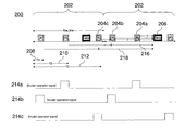
- FIG. 2 is a timing chart 200 illustrating the relationship between the above-described shutter and sampling operations over multiple row time periods of image sensing device 100 .
- Multiple row time periods 202 are illustrated in FIG. 2 .
- controller 140 performs a shutter operation (as described above), shown as blocks 204 .
- controller 140 performs a sampling operation (as described above), shown as blocks 206 .
- the predetermined duration (or integration time) between each the shutter operation and the following sampling operation is less than the row time period 202 of image sensing device 100 .
- the length of the integration time is illustrated by line 208 .
- the length of the integration time is illustrated by line 210 .
- the length of the integration time is illustrated by line 212 .
- none of integration times 208 , 210 , 212 is equal in duration to row time period 202 or an integer multiple of the row time period.
- image sensing device 100 may be configured to perform a shutter operation at different times during each row time period 202 .
- Different modes of operation 214 are shown in FIG. 2 .
- controller 140 sends signals to image sensor 120 to perform shutter operations 204 a during exposure
- controller 140 sends signals to image sensor 120 to perform shutter operations 204 b during exposure
- controller 140 sends signals to image sensor 120 to perform shutter operations 204 c during exposure.
- controller 140 may be programmed to delay the addressing of the row of pixels for which a shutter or sampling operation must be performed. As shown in FIG. 2 , the integration time for line 218 may be equal to one row time period plus the integration time for line 210 . If desired, the delay can be extended to multiple rows.
- FIG. 3 is a flowchart illustrating an example method 300 for sensing images with an image sensing device in accordance with aspects of the present invention.
- the image sensing device may be an electronic device such as, for example, a digital camera.
- method 300 includes performing a shutter operation for a row of pixels and sampling the row of pixels. Additional details of method 300 are described herein with respect to the components of image sensing device 100 .
- a shutter operation is performed for a row of pixels.
- controller 140 performs a shutter operation for a row of pixels 122 in image sensor 120 .
- the shutter operation may be a rolling shutter operation across each of the rows of pixels 122 , as described above.
- step 320 the row of pixels is sampled after a predetermined duration following the performance of the shutter operation.
- controller 140 samples the row of pixels after a predetermined duration following the shutter operation.
- the predetermined duration is different from the row time period of image sensing device 100 , and more particularly, is different from any multiple of the row time period of image sensing device 100 .
- aspects of the present invention relate to methods and devices for improving dynamic range in image sensors.
- a method for sensing images with an image sensing device comprises an image sensor having a plurality of rows of pixels.
- the method comprises performing a shutter operation for one of the plurality of rows of pixels, and sampling the one of the plurality of rows after a predetermined duration following the performance of the shutter operation.
- the predetermined duration is different from a multiple of a row time period of the image sensing device.
- an image sensing device comprises an image sensor having a plurality of rows of pixels, and a controller for controlling the exposure of each row of pixels.
- the controller is programmed to perform the above-described method.
Landscapes
- Engineering & Computer Science (AREA)
- Multimedia (AREA)
- Signal Processing (AREA)
- Transforming Light Signals Into Electric Signals (AREA)
- Solid State Image Pick-Up Elements (AREA)
Abstract
Description
Claims (6)
Priority Applications (4)
| Application Number | Priority Date | Filing Date | Title |
|---|---|---|---|
| US13/249,881 US8994859B2 (en) | 2011-09-30 | 2011-09-30 | Methods and devices for improving dynamic range in image sensors |
| TW101136096A TWI533695B (en) | 2011-09-30 | 2012-09-28 | Methods and devices for improving dynamic range in image sensors |
| CN201210370743.9A CN103037176B (en) | 2011-09-30 | 2012-09-28 | For improving the method and apparatus of the dynamic range of imageing sensor |
| DE102012217809.0A DE102012217809B4 (en) | 2011-09-30 | 2012-09-28 | Method and device for improving the dynamic range in image sensors |
Applications Claiming Priority (1)
| Application Number | Priority Date | Filing Date | Title |
|---|---|---|---|
| US13/249,881 US8994859B2 (en) | 2011-09-30 | 2011-09-30 | Methods and devices for improving dynamic range in image sensors |
Publications (2)
| Publication Number | Publication Date |
|---|---|
| US20130083236A1 US20130083236A1 (en) | 2013-04-04 |
| US8994859B2 true US8994859B2 (en) | 2015-03-31 |
Family
ID=47878844
Family Applications (1)
| Application Number | Title | Priority Date | Filing Date |
|---|---|---|---|
| US13/249,881 Active 2033-07-31 US8994859B2 (en) | 2011-09-30 | 2011-09-30 | Methods and devices for improving dynamic range in image sensors |
Country Status (4)
| Country | Link |
|---|---|
| US (1) | US8994859B2 (en) |
| CN (1) | CN103037176B (en) |
| DE (1) | DE102012217809B4 (en) |
| TW (1) | TWI533695B (en) |
Citations (10)
| Publication number | Priority date | Publication date | Assignee | Title |
|---|---|---|---|---|
| US20060192867A1 (en) | 2005-02-01 | 2006-08-31 | Transchip, Inc | Variable exposure for color image sensor |
| US20080044170A1 (en) | 2006-08-16 | 2008-02-21 | Choon Hwee Yap | Image Capturing System And Method Of Operating The Same |
| CN101292358A (en) | 2005-08-24 | 2008-10-22 | 美光科技公司 | Solid-state imager with capacitors above red pixels |
| CN101350890A (en) | 2007-08-31 | 2009-01-21 | 豪威科技有限公司 | Image sensor with high dynamic range under downsampling mode |
| US20100309340A1 (en) * | 2009-06-03 | 2010-12-09 | Border John N | Image sensor having global and rolling shutter processes for respective sets of pixels of a pixel array |
| US20110019051A1 (en) * | 2009-07-24 | 2011-01-27 | Zhiping Yin | Image sensors with pixel charge summing |
| US20110242351A1 (en) * | 2010-03-30 | 2011-10-06 | Sony Corporation | Solid-state imaging device and imaging device |
| US20120175498A1 (en) * | 2011-01-10 | 2012-07-12 | Alexander Krymski | Image sensors and methods with shared control lines |
| US20120300105A1 (en) * | 2009-04-01 | 2012-11-29 | Omnivision Technologies, Inc. | Exposing pixel groups in producing digital images |
| US20120314124A1 (en) * | 2011-06-13 | 2012-12-13 | Sony Corporation | Image pickup apparatus, image pickup apparatus control method, and program |
Family Cites Families (2)
| Publication number | Priority date | Publication date | Assignee | Title |
|---|---|---|---|---|
| US7554588B2 (en) * | 2005-02-01 | 2009-06-30 | TransChip Israel, Ltd. | Dual exposure for image sensor |
| US7855740B2 (en) * | 2007-07-20 | 2010-12-21 | Eastman Kodak Company | Multiple component readout of image sensor |
-
2011
- 2011-09-30 US US13/249,881 patent/US8994859B2/en active Active
-
2012
- 2012-09-28 DE DE102012217809.0A patent/DE102012217809B4/en active Active
- 2012-09-28 TW TW101136096A patent/TWI533695B/en active
- 2012-09-28 CN CN201210370743.9A patent/CN103037176B/en active Active
Patent Citations (11)
| Publication number | Priority date | Publication date | Assignee | Title |
|---|---|---|---|---|
| US20060192867A1 (en) | 2005-02-01 | 2006-08-31 | Transchip, Inc | Variable exposure for color image sensor |
| US20110261237A1 (en) * | 2005-02-01 | 2011-10-27 | Samsung Electronics Co., Ltd. | Variable exposure for color image sensor |
| CN101292358A (en) | 2005-08-24 | 2008-10-22 | 美光科技公司 | Solid-state imager with capacitors above red pixels |
| US20080044170A1 (en) | 2006-08-16 | 2008-02-21 | Choon Hwee Yap | Image Capturing System And Method Of Operating The Same |
| CN101350890A (en) | 2007-08-31 | 2009-01-21 | 豪威科技有限公司 | Image sensor with high dynamic range under downsampling mode |
| US20120300105A1 (en) * | 2009-04-01 | 2012-11-29 | Omnivision Technologies, Inc. | Exposing pixel groups in producing digital images |
| US20100309340A1 (en) * | 2009-06-03 | 2010-12-09 | Border John N | Image sensor having global and rolling shutter processes for respective sets of pixels of a pixel array |
| US20110019051A1 (en) * | 2009-07-24 | 2011-01-27 | Zhiping Yin | Image sensors with pixel charge summing |
| US20110242351A1 (en) * | 2010-03-30 | 2011-10-06 | Sony Corporation | Solid-state imaging device and imaging device |
| US20120175498A1 (en) * | 2011-01-10 | 2012-07-12 | Alexander Krymski | Image sensors and methods with shared control lines |
| US20120314124A1 (en) * | 2011-06-13 | 2012-12-13 | Sony Corporation | Image pickup apparatus, image pickup apparatus control method, and program |
Also Published As
| Publication number | Publication date |
|---|---|
| CN103037176A (en) | 2013-04-10 |
| TWI533695B (en) | 2016-05-11 |
| TW201320732A (en) | 2013-05-16 |
| US20130083236A1 (en) | 2013-04-04 |
| DE102012217809B4 (en) | 2020-02-06 |
| DE102012217809A1 (en) | 2013-04-04 |
| CN103037176B (en) | 2016-03-30 |
Similar Documents
| Publication | Publication Date | Title |
|---|---|---|
| US11595600B2 (en) | Method, apparatus and system providing a storage gate pixel with high dynamic range | |
| US12231788B2 (en) | Method, apparatus, and system providing an imager with pixels having extended dynamic range | |
| TWI424742B (en) | Method and device for high dynamic operation of pixel unit | |
| US8582011B2 (en) | Simultaneous global shutter and correlated double sampling read out in multiple photosensor pixels | |
| US8289425B2 (en) | Solid-state image pickup device with an improved output amplifier circuitry | |
| CN108419032B (en) | HDR image sensor pixel structure and imaging system supporting multiple exposure modes | |
| CN111327845A (en) | Image sensor and driving method thereof | |
| JP2009505438A (en) | High dynamic range / blooming-resistant common gate on pixels shared in multiple directions | |
| US8115841B2 (en) | Method, apparatus and system providing an image sensor having pixels with multiple exposures, diodes and gain readouts | |
| CN1833429A (en) | Dual conversion gain imagers | |
| US9118851B2 (en) | High dynamic range image sensor read out architecture | |
| US9137432B2 (en) | Backside illumination image sensor, operating method thereof, image processing system and method of processing image using the same | |
| US10051216B2 (en) | Imaging apparatus and imaging method thereof using correlated double sampling | |
| TWI382750B (en) | Method and device for reducing dark current in image sensor | |
| US8994859B2 (en) | Methods and devices for improving dynamic range in image sensors | |
| KR100494100B1 (en) | Cmos image sensor |
Legal Events
| Date | Code | Title | Description |
|---|---|---|---|
| AS | Assignment |
Owner name: APTINA IMAGING CORPORATION, CAYMAN ISLANDS Free format text: ASSIGNMENT OF ASSIGNORS INTEREST;ASSIGNOR:YAGHMAI, SOHRAB;REEL/FRAME:027063/0987 Effective date: 20110927 |
|
| AS | Assignment |
Owner name: SEMICONDUCTOR COMPONENTS INDUSTRIES, LLC, ARIZONA Free format text: ASSIGNMENT OF ASSIGNORS INTEREST;ASSIGNOR:APTINA IMAGING CORPORATION;REEL/FRAME:034673/0001 Effective date: 20141217 |
|
| STCF | Information on status: patent grant |
Free format text: PATENTED CASE |
|
| AS | Assignment |
Owner name: DEUTSCHE BANK AG NEW YORK BRANCH, NEW YORK Free format text: SECURITY INTEREST;ASSIGNOR:SEMICONDUCTOR COMPONENTS INDUSTRIES, LLC;REEL/FRAME:038620/0087 Effective date: 20160415 |
|
| AS | Assignment |
Owner name: DEUTSCHE BANK AG NEW YORK BRANCH, AS COLLATERAL AGENT, NEW YORK Free format text: CORRECTIVE ASSIGNMENT TO CORRECT THE INCORRECT PATENT NUMBER 5859768 AND TO RECITE COLLATERAL AGENT ROLE OF RECEIVING PARTY IN THE SECURITY INTEREST PREVIOUSLY RECORDED ON REEL 038620 FRAME 0087. ASSIGNOR(S) HEREBY CONFIRMS THE SECURITY INTEREST;ASSIGNOR:SEMICONDUCTOR COMPONENTS INDUSTRIES, LLC;REEL/FRAME:039853/0001 Effective date: 20160415 Owner name: DEUTSCHE BANK AG NEW YORK BRANCH, AS COLLATERAL AG Free format text: CORRECTIVE ASSIGNMENT TO CORRECT THE INCORRECT PATENT NUMBER 5859768 AND TO RECITE COLLATERAL AGENT ROLE OF RECEIVING PARTY IN THE SECURITY INTEREST PREVIOUSLY RECORDED ON REEL 038620 FRAME 0087. ASSIGNOR(S) HEREBY CONFIRMS THE SECURITY INTEREST;ASSIGNOR:SEMICONDUCTOR COMPONENTS INDUSTRIES, LLC;REEL/FRAME:039853/0001 Effective date: 20160415 |
|
| MAFP | Maintenance fee payment |
Free format text: PAYMENT OF MAINTENANCE FEE, 4TH YEAR, LARGE ENTITY (ORIGINAL EVENT CODE: M1551); ENTITY STATUS OF PATENT OWNER: LARGE ENTITY Year of fee payment: 4 |
|
| MAFP | Maintenance fee payment |
Free format text: PAYMENT OF MAINTENANCE FEE, 8TH YEAR, LARGE ENTITY (ORIGINAL EVENT CODE: M1552); ENTITY STATUS OF PATENT OWNER: LARGE ENTITY Year of fee payment: 8 |
|
| AS | Assignment |
Owner name: FAIRCHILD SEMICONDUCTOR CORPORATION, ARIZONA Free format text: RELEASE OF SECURITY INTEREST IN PATENTS RECORDED AT REEL 038620, FRAME 0087;ASSIGNOR:DEUTSCHE BANK AG NEW YORK BRANCH, AS COLLATERAL AGENT;REEL/FRAME:064070/0001 Effective date: 20230622 Owner name: SEMICONDUCTOR COMPONENTS INDUSTRIES, LLC, ARIZONA Free format text: RELEASE OF SECURITY INTEREST IN PATENTS RECORDED AT REEL 038620, FRAME 0087;ASSIGNOR:DEUTSCHE BANK AG NEW YORK BRANCH, AS COLLATERAL AGENT;REEL/FRAME:064070/0001 Effective date: 20230622 |