US20140286381A1 - Receiver circuit and semiconductor integrated circuit - Google Patents
Receiver circuit and semiconductor integrated circuit Download PDFInfo
- Publication number
- US20140286381A1 US20140286381A1 US14/170,901 US201414170901A US2014286381A1 US 20140286381 A1 US20140286381 A1 US 20140286381A1 US 201414170901 A US201414170901 A US 201414170901A US 2014286381 A1 US2014286381 A1 US 2014286381A1
- Authority
- US
- United States
- Prior art keywords
- circuit
- sampling
- phase
- amplitude level
- bit value
- Prior art date
- Legal status (The legal status is an assumption and is not a legal conclusion. Google has not performed a legal analysis and makes no representation as to the accuracy of the status listed.)
- Granted
Links
- 239000004065 semiconductor Substances 0.000 title claims description 4
- 238000001514 detection method Methods 0.000 claims abstract description 119
- 238000000034 method Methods 0.000 claims abstract description 54
- 230000008569 process Effects 0.000 claims abstract description 21
- 238000005070 sampling Methods 0.000 claims description 256
- 230000003044 adaptive effect Effects 0.000 description 25
- 230000007246 mechanism Effects 0.000 description 12
- 230000004048 modification Effects 0.000 description 12
- 238000012986 modification Methods 0.000 description 12
- 238000012544 monitoring process Methods 0.000 description 11
- 230000006870 function Effects 0.000 description 10
- 230000005540 biological transmission Effects 0.000 description 7
- 230000008859 change Effects 0.000 description 7
- 238000004364 calculation method Methods 0.000 description 4
- 230000003247 decreasing effect Effects 0.000 description 4
- 230000000630 rising effect Effects 0.000 description 4
- 238000001914 filtration Methods 0.000 description 3
- 230000008901 benefit Effects 0.000 description 2
- 230000002542 deteriorative effect Effects 0.000 description 2
- 230000007717 exclusion Effects 0.000 description 2
- 238000004519 manufacturing process Methods 0.000 description 2
- 238000011084 recovery Methods 0.000 description 2
- 238000007476 Maximum Likelihood Methods 0.000 description 1
- 108010076504 Protein Sorting Signals Proteins 0.000 description 1
- 230000004075 alteration Effects 0.000 description 1
- 238000005311 autocorrelation function Methods 0.000 description 1
- 230000015572 biosynthetic process Effects 0.000 description 1
- 230000006866 deterioration Effects 0.000 description 1
- 238000002474 experimental method Methods 0.000 description 1
- 230000006872 improvement Effects 0.000 description 1
- 230000010365 information processing Effects 0.000 description 1
- 238000005457 optimization Methods 0.000 description 1
- 230000008520 organization Effects 0.000 description 1
- 238000012545 processing Methods 0.000 description 1
- 229920006395 saturated elastomer Polymers 0.000 description 1
- 238000006467 substitution reaction Methods 0.000 description 1
- 238000003786 synthesis reaction Methods 0.000 description 1
Images

Classifications
-
- H—ELECTRICITY
- H04—ELECTRIC COMMUNICATION TECHNIQUE
- H04L—TRANSMISSION OF DIGITAL INFORMATION, e.g. TELEGRAPHIC COMMUNICATION
- H04L1/00—Arrangements for detecting or preventing errors in the information received
- H04L1/20—Arrangements for detecting or preventing errors in the information received using signal quality detector
-
- H—ELECTRICITY
- H04—ELECTRIC COMMUNICATION TECHNIQUE
- H04L—TRANSMISSION OF DIGITAL INFORMATION, e.g. TELEGRAPHIC COMMUNICATION
- H04L7/00—Arrangements for synchronising receiver with transmitter
- H04L7/02—Speed or phase control by the received code signals, the signals containing no special synchronisation information
- H04L7/033—Speed or phase control by the received code signals, the signals containing no special synchronisation information using the transitions of the received signal to control the phase of the synchronising-signal-generating means, e.g. using a phase-locked loop
- H04L7/0334—Processing of samples having at least three levels, e.g. soft decisions
-
- H—ELECTRICITY
- H03—ELECTRONIC CIRCUITRY
- H03L—AUTOMATIC CONTROL, STARTING, SYNCHRONISATION OR STABILISATION OF GENERATORS OF ELECTRONIC OSCILLATIONS OR PULSES
- H03L7/00—Automatic control of frequency or phase; Synchronisation
- H03L7/06—Automatic control of frequency or phase; Synchronisation using a reference signal applied to a frequency- or phase-locked loop
- H03L7/08—Details of the phase-locked loop
- H03L7/085—Details of the phase-locked loop concerning mainly the frequency- or phase-detection arrangement including the filtering or amplification of its output signal
- H03L7/089—Details of the phase-locked loop concerning mainly the frequency- or phase-detection arrangement including the filtering or amplification of its output signal the phase or frequency detector generating up-down pulses
-
- H—ELECTRICITY
- H04—ELECTRIC COMMUNICATION TECHNIQUE
- H04L—TRANSMISSION OF DIGITAL INFORMATION, e.g. TELEGRAPHIC COMMUNICATION
- H04L25/00—Baseband systems
- H04L25/02—Details ; arrangements for supplying electrical power along data transmission lines
- H04L25/03—Shaping networks in transmitter or receiver, e.g. adaptive shaping networks
- H04L25/03006—Arrangements for removing intersymbol interference
- H04L25/03012—Arrangements for removing intersymbol interference operating in the time domain
- H04L25/03019—Arrangements for removing intersymbol interference operating in the time domain adaptive, i.e. capable of adjustment during data reception
- H04L25/03057—Arrangements for removing intersymbol interference operating in the time domain adaptive, i.e. capable of adjustment during data reception with a recursive structure
Definitions
- the embodiments discussed herein are related to a receiver circuit and a semiconductor integrated circuit.
- a technique called baud rate tracking CDR is known as one of techniques for realizing the tracking CDR. With this technique 1-bit data is sampled once.
- a technique for calculating an autocorrelation function of a signal sequence obtained by sampling a data signal at a sampling rate which is equal to a transmission baud rate and controlling a sampling phase so as to maximize a calculated value is proposed as an example.
- a technique called 2 ⁇ tracking CDR is known.
- 1-bit data is sampled twice.
- a technique for preparing a clock other than a data detection clock to detect an edge portion (zero-crossing point) of a data signal and detecting a deviation of phase between the data detection clock and the data signal on the basis of an amplitude level detected by the clock is proposed.
- the phase deviation is detected with the amplitude level at the zero-crossing point of the data signal as reference. This curbs the influence of variations in the amplitude of a data signal caused by the influence of transmission line loss, noise, or the like on detection accuracy. Accordingly, a phase deviation can be detected with greater accuracy.
- a special sampling circuit which samples a data signal by a clock other than a data detection clock is included. That is to say, a special sampling circuit for detecting an amplitude level at a zero-crossing point of a data signal is included, so circuit size increases.
- a receiver circuit including a sampling circuit which detects an amplitude level of an input data signal at a sampling timing indicated by a sampling clock, a first comparison circuit which compares a first amplitude level and a second amplitude level detected by the sampling circuit at a first sampling timing and a second sampling timing, respectively, with a determined threshold, an interpolation circuit which calculates an intermediate level that approximates to an amplitude level of the input data signal corresponding to an intermediate point between the first sampling timing and the second sampling timing by an interpolation process based on the first amplitude level and the second amplitude level, a second comparison circuit which compares the intermediate level with the determined threshold, and a phase deviation detection circuit which detects a deviation of phase between the sampling clock and the input data signal on the basis of results of comparisons made by the first comparison circuit and the second comparison circuit.
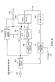
- FIG. 1 is an example of a receiver circuit according to a first embodiment
- FIG. 2 illustrates a phase deviation detection method according to a second embodiment
- FIG. 3 is an example of a receiver circuit according to the second embodiment
- FIG. 4 is an example of a process performed by each comparison circuit in the second embodiment
- FIG. 5 is an example of a phase detection circuit in the second embodiment
- FIG. 6 indicates the relationships among inputs to and outputs from the phase detection circuit in the second embodiment
- FIG. 7 is an example of a 4-bit pattern filter in the second embodiment
- FIG. 8 is an example of a receiver circuit according to a third embodiment
- FIG. 9 is an example of an equalizer (m-tap DFE) in the third embodiment.
- FIG. 10 is an example of an equalizer (1-tap Speculative DFE) in the third embodiment
- FIG. 11 indicates a filter pattern switching method in the third embodiment
- FIG. 12 is a first example of a receiver circuit according to a fourth embodiment
- FIG. 13 illustrates examples of sampling circuits and data interpolation circuits in the fourth embodiment
- FIG. 14 indicates operation timing of each switch included in the sampling circuits and the data interpolation circuits in the fourth embodiment
- FIG. 15 indicates a change in node potential and a change in outputted amplitude level in the sampling circuits and the data interpolation circuits in the fourth embodiment
- FIG. 16 is a second example of the receiver circuit according to the fourth embodiment.
- FIG. 17 is an example of a receiver circuit including a BR phase detector having an amplitude adjustment function.
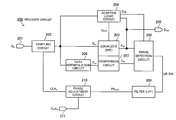
- a receiver circuit 10 according to a first embodiment will be described with reference to FIG. 1 .
- FIG. 1 is an example of a receiver circuit according to a first embodiment.
- a receiver circuit 10 includes a sampling circuit 11 , a first comparison circuit 12 , an interpolation circuit 13 , a second comparison circuit 14 , and a phase deviation detection circuit 15 .
- the receiver circuit 10 includes a filter 16 and a phase adjustment circuit 17 .
- the sampling circuit 11 detects an amplitude level of an input data signal D in at a sampling timing indicated by a sampling clock.
- an amplitude level of the input data signal D in is sampled at a first sampling timing and a second sampling timing.
- the sampling circuit 11 detects a first amplitude level D sc [n ⁇ 1] at the first sampling timing and detects a second amplitude level D sc [n] at the second sampling timing.
- the first amplitude level D sc [n ⁇ 1] and the second amplitude level D sc [n] detected by the sampling circuit 11 are inputted to the first comparison circuit 12 and the interpolation circuit 13 .
- the first comparison circuit 12 compares the first amplitude level D sc [n ⁇ 1] and the second amplitude level D sc [n] detected by the sampling circuit 11 at the first sampling timing and the second sampling timing, respectively, with a determined threshold Th.
- the determined threshold Th is set to an intermediate value of an amplitude level of the input data signal D m .
- the determined threshold Th is set to a level which passes through the center of an eye (or a zero-crossing point) on an eye pattern.
- the first amplitude level D sc [n ⁇ 1] and the second amplitude level D sc [n] are compared with the determined threshold Th at a falling edge portion of the input data signal D in .
- the first amplitude level D sc [n ⁇ 1] is higher than the determined threshold Th, so the first comparison circuit 12 outputs “1” as a first bit value D dc [n ⁇ 1] which is a comparison result on the first amplitude level D sc [n ⁇ 1].
- the second amplitude level D sc [n] is lower than the determined threshold Th, so the first comparison circuit 12 outputs “0” as a second bit value D dc [n] which is a comparison result on the second amplitude level D sc [n].
- the first bit value D dc [n ⁇ 1] and the second bit value D dc [n], which are the results of the comparisons made by the first comparison circuit 12 , are outputted in order to the outside as data D out . Furthermore, the first bit value D dc [n ⁇ 1] and the second bit value D dc [n] are inputted in order to the phase deviation detection circuit 15 .
- the interpolation circuit 13 calculates an intermediate level D sc [n] which approximates to an amplitude level of the input data signal D in corresponding to an intermediate point between the first sampling timing and the second sampling timing by an interpolation process based on the first amplitude level D sc [n ⁇ 1] and the second amplitude level D sc [n].
- the first comparison circuit 12 performs a comparison process on the first amplitude level D sc [n ⁇ 1] and the second amplitude level D sc [n] inputted in order.
- the interpolation circuit 13 holds the first amplitude level D sc [n ⁇ 1] inputted first, and calculates the intermediate level D sc [n] at a timing at which the second amplitude level D sc [n] is inputted after. Therefore, the interpolation circuit 13 includes a holding section (not illustrated) for holding the first amplitude level D sc [n ⁇ 1].
- the intermediate level D se [n] calculated by the interpolation circuit 13 is inputted to the second comparison circuit 14 .
- the second comparison circuit 14 compares the intermediate level D se [n] with a determined threshold Th.
- the determined threshold Th used by the second comparison circuit 14 is equal in value to the determined threshold Th used by the first comparison circuit 12 .
- a phase of the sampling clock is slower than a phase of the input data signal D in .
- an amplitude level detected at the falling edge portion (amplitude level at a zero-crossing point) of the input data signal D in at the intermediate point between the first sampling timing and the second sampling timing is lower than the determined threshold Th.
- the intermediate level D se [n] which approximates to the amplitude level at the zero-crossing point is also lower than the determined threshold Th. Accordingly, the second comparison circuit 14 outputs “0” as a bit value D de [n] which is a comparison result on the intermediate level D se [n].
- the bit value D de [n] which is the result of the comparison made by the second comparison circuit 14 , is inputted to the phase deviation detection circuit 15 .
- the phase deviation detection circuit 15 detects a deviation of phase between the sampling clock and the input data signal D in on the basis of the first bit value D dc [n ⁇ 1], the second bit value D dc [n], and the bit value D de [n].
- the first bit value D dc [n ⁇ 1] is “1” and the second bit value D dc [n] is “0”. This indicates a falling edge portion of the input data signal D in .
- the bit value D de [n] is “0”. This indicates that a phase of the sampling clock is slower than a phase of the input data signal D in .
- each circuit For convenience of explanation the function and operation of each circuit have been described with attention paid to the first sampling timing and the second sampling timing.
- a phase deviation is detected and adjusted in order according to an amplitude level of the input data signal D in sampled at each sampling timing in the same way that is described above.
- a high-frequency component of an UP/DN signal outputted from the phase deviation detection circuit 15 is removed by the filter 16 .
- the UP/DN signal is inputted to the phase adjustment circuit 17 as a phase adjustment signal Ph code .
- the phase adjustment circuit 17 adjusts a phase of a clock CLK in supplied from the outside according to the phase adjustment signal Ph code and supplies to the sampling circuit 11 a sampling clock CLK s which is a clock after the adjustment.
- the receiver circuit 10 can realize the function of correcting a deviation of phase between the input data signal D in and the sampling clock.
- the receiver circuit makes the interpolation circuit 13 calculate the intermediate level D se [n] which approximates to an amplitude level at the zero-crossing point by an interpolation process and makes the phase deviation detection circuit 15 detect a phase deviation by the use of the intermediate level D se [n]. Accordingly, a special sampling circuit for detecting an amplitude level at the zero-crossing point is not included. This checks an increase in circuit scale. Furthermore, a phase deviation is detected by the use of the intermediate level D se [n].
- the receiver circuit 10 may be connected to a logic circuit 20 to form a semiconductor integrated circuit 5 .
- FIG. 2 illustrates a phase deviation detection method according to a second embodiment.
- FIG. 2 schematically illustrates an eye pattern of an input data signal D in .
- the input data signal D in is sampled at a sampling timing which is near the center of an eye on the eye pattern.
- the input data signal D in is sampled at a sampling timing TD n ⁇ 1 and a sampling timing TD n (cycle of sampling timing is set to a constant value).
- a timing TC n which is intermediate between the sampling timing TD n ⁇ 1 and the sampling timing TD n is referred to as a zero-crossing point.
- a threshold Th used for deciding data from an amplitude level of the input data signal D in is set to a level (which may be referred to as a zero level) which passes through the center of the eye on the eye pattern. It is assumed that if an amplitude level is higher than the threshold Th, the decision that a bit value is “1” is made, and that if an amplitude level is lower than the threshold Th, the decision that a bit value is “0” is made.
- FIG. 2 illustrates a signal waveform obtained in case (A) where a phase of a sampling clock is slower than a phase of the input data signal D in and a signal waveform obtained in case (B) where a phase of the sampling clock is faster than a phase of the input data signal D in .
- a phase of the sampling clock is slow at a falling edge portion of the input data signal D in , that is to say, in the case of (A)
- an amplitude level at the zero-crossing point of the input data signal D in is higher than the threshold Th.
- a phase of the sampling clock is fast, that is to say, in the case of (B)
- an amplitude level at the zero-crossing point of the input data signal D in is lower than the threshold Th.
- an edge portion of the input data signal D in is a falling edge portion or a rising edge portion is decided and whether or not an amplitude level at the zero-crossing point of the input data signal D in is higher than the threshold Th is decided.
- a phase deviation of the sampling clock can be detected. Even if the amplitude of the input data signal D in varies by the influence of transmission line loss, process variations at production time, temperature variations at operation time, noise, or the like, an amplitude level of the input data signal D in detected at the zero-crossing point does not change much. Accordingly, by detecting a phase deviation by the use of an amplitude level at the zero-crossing point of the input data signal D in , the influence of the variations in the amplitude of the input data signal D in on detection accuracy is reduced.
- the method of detecting a phase deviation with an amplitude level at the zero-crossing point of the input data signal D in as reference is adopted.
- the input data signal D in is not sampled at the zero-crossing point.
- Amplitude levels of the input data signal D in sampled at the sampling timing TD n ⁇ 1 and the sampling timing TD n are used.
- amplitude levels D sc [n ⁇ 1] and D sc [n] detected at the sampling timing TD n ⁇ 1 and the sampling timing TD n , respectively, are used for performing an interpolation process, and an intermediate level D se [n] which approximates to an amplitude level at the zero-crossing point of the input data signal D in is used. That is to say, the intermediate level D se [n] is compared with the threshold Th and a phase deviation of the sampling clock is detected.
- the amplitude level D sc [n ⁇ 1] is higher than the threshold Th at the falling edge portion of the input data signal D in . Furthermore, the amplitude level D sc [n] is lower than the threshold Th at the falling edge portion of the input data signal D in .
- a bit value D dc [n ⁇ 1] indicative of a comparison result on the amplitude level D sc [n ⁇ 1] is “1” and a bit value D dc [n] indicative of a comparison result on the amplitude level D sc [n] is “0”.
- the amplitude level D sc [n ⁇ 1] is lower than the threshold Th at a rising edge portion of the input data signal D in . Furthermore, the amplitude level D sc [n] is higher than the threshold Th at the rising edge portion of the input data signal D in .
- the bit value D dc [n ⁇ 1] indicative of a comparison result on the amplitude level D sc [n ⁇ 1] is “0” and the bit value D dc [n] indicative of a comparison result on the amplitude level D sc [n] is “1”.
- the intermediate level D se [n] is lower than the threshold Th and the bit value D se [n] indicative of a comparison result on the intermediate level D se [n] is Conversely, if a phase of the sampling clock is fast, the intermediate level D se [n] is higher than the threshold Th and the bit value D de [n] indicative of a comparison result on the intermediate level D se [n] is “1”.
- a phase deviation of the sampling clock can be detected in this way by a combination of the bit values D dc [n ⁇ 1], D de [n], and D dc [n].
- a table in which such combinations are enumerated is indicated in the lowermost part of FIG. 2 .
- An UP/DN column is included in the table indicated in FIG. 2 .
- a value in the UP/DN column indicates a direction in which a phase of the sampling clock is adjusted. For example, if an UP/DN signal is “+1”, then an adjustment is made in a direction in which a phase of the sampling clock is set forward. On the other hand, if an UP/DN signal is “ ⁇ 1”, then an adjustment is made in a direction in which a phase of the sampling clock is set back.
- a combination of the bit value D dc [n ⁇ 1] “0”, the bit value D de [n] “0”, and the bit value D dc [n] “1” indicates that a phase of the sampling clock is fast. Accordingly, an UP/DN signal is set to “ ⁇ 1” so as to make an adjustment for setting back a phase of the sampling clock. Conversely, a combination of the bit value D dc [n ⁇ 1] “0”, the bit value D de [n] “1”, and the bit value D dc [n] “1” indicates that a phase of the sampling clock is slow. Accordingly, an UP/DN signal is set to “+1” so as to make an adjustment for setting forward a phase of the sampling clock.
- a combination of the bit value D dc [n ⁇ 1] “1”, the bit value D de [n] “0”, and the bit value D dc [n]“0” indicates that a phase of the sampling clock is slow. Accordingly, an UP/DN signal is set to “+1” so as to make an adjustment for setting forward a phase of the sampling clock. Conversely, a combination of the bit value D dc [n ⁇ 1] “1”, the bit value D de [n] “1”, and the bit value D dc [n] “0” indicates that a phase of the sampling clock is fast. Accordingly, an UP/DN signal is set to “ ⁇ 1” so as to make an adjustment for setting back a phase of the sampling clock.
- phase deviation detection method The overview of the phase deviation detection method according to the second embodiment has been given.
- An example of a receiver circuit by which the phase deviation detection method can be realized, its operation, and the like will now be described.
- a phase deviation of the sampling clock is detected by a pattern obtained by combining 2-bit values.
- a method for adjusting a phase deviation of a sampling clock by the use of a pattern obtained by combining 4-bit values will also be described later.
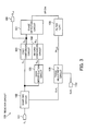
- FIG. 3 is an example of a receiver circuit according to the second embodiment.
- a receiver circuit 100 includes a data input terminal 101 , a sampling circuit 102 , a first comparison circuit 103 , and a data output terminal 104 .
- the receiver circuit 100 includes a data interpolation circuit 105 , a second comparison circuit 106 , a phase detection circuit 107 , a filter 108 , a phase adjustment circuit 109 , and a clock input terminal 110 .
- An input data signal D in is inputted to the data input terminal 101 .
- the input data signal D in is inputted to the sampling circuit 102 .
- the sampling circuit 102 detects an amplitude level D sc of the input data signal D in at a sampling timing indicated by a sampling clock CLK s .
- the amplitude level D sc of the input data signal D in detected by the sampling circuit 102 at a sampling timing TD n may be represented as D sc [n].
- the amplitude level D sc detected by the sampling circuit 102 is inputted to the first comparison circuit 103 and the data interpolation circuit 105 .
- the first comparison circuit 103 compares the amplitude level D sc inputted from the sampling circuit 102 with a determined threshold Th. If the amplitude level D sc is higher than the determined threshold Th, then the first comparison circuit 103 outputs the bit value “1” as a comparison result D dc . If the amplitude level D sc is lower than the determined threshold Th, then the first comparison circuit 103 outputs the bit value “0” as a comparison result D dc .
- the bit value D dc indicative of a comparison result is outputted as received data D out from the data output terminal 104 to the outside of the receiver circuit 100 . In addition, the bit value D dc is inputted to the phase detection circuit 107 .
- the data interpolation circuit 105 holds the amplitude level D sc inputted from the sampling circuit 102 in a holding section (not illustrated).
- the data interpolation circuit 105 performs an interpolation process by the use of two amplitude levels D sc detected at two sampling timings to find an intermediate level D se which approximates to an amplitude level of the input data signal D in at an intermediate point (zero-crossing point) between the two sampling timings. For example, the data interpolation circuit 105 finds an intermediate value between the two amplitude levels D sc and considers the found intermediate value as the intermediate level D se .
- the method of finding the intermediate level D se [n] for the two adjacent sampling timings TD n ⁇ 1 and TD n is indicated.
- the two sampling timings may not be adjacent to each other.
- the data interpolation circuit 105 may consider as the intermediate level D se an intermediate value between amplitude levels D sc [n ⁇ 2] and D sc [n+1] of the input data signal D in detected at two sampling timings TD n ⁇ 2 and TD n+1 .
- a linear interpolation is used as an interpolation method.
- a nonlinear interpolation such as a polynomial interpolation or a spline interpolation, may be used.
- the data interpolation circuit 105 uses amplitude levels D sc detected at three or more sampling timings.
- a flip-flop circuit or the like may be used as the holding section.
- the method of holding an amplitude level D sc by the use of capacitance (method of directly finding an intermediate level D se by devising a capacitance ratio) may be used as with a circuit illustrated in FIG. 13 (described later).
- the intermediate level D se found by the data interpolation circuit 105 is inputted to the second comparison circuit 106 .
- the second comparison circuit 106 compares the intermediate level D se inputted from the data interpolation circuit 105 with the determined threshold Th. If the intermediate level D se is higher than the determined threshold Th, then the second comparison circuit 106 outputs the bit value “1” as a comparison result D de . If the intermediate level D se is lower than the determined threshold Th, then the second comparison circuit 106 outputs the bit value “0” as a comparison result D de .
- the bit value D de indicative of a comparison result is inputted to the phase detection circuit 107 .
- the phase detection circuit 107 detects a phase deviation of the sampling clock on the basis of the bit value D dc inputted from the first comparison circuit 103 and the bit value D de inputted from the second comparison circuit 106 . As indicated in FIG. 2 , the phase detection circuit 107 decides a direction of the phase deviation from a combination of a bit value D de and two bit values D dc corresponding thereto, and outputs an UP/DN signal indicative of a decision result. In addition to a bit value D de and two bit values D dc corresponding thereto, the phase detection circuit 107 may take another bit value D dc or other bit values D dc into consideration to detect a phase deviation. Such a modification will be described later.
- phase detection circuit 107 decides that a phase of the sampling clock is slow, then the phase detection circuit 107 outputs an UP/DN signal (+1) for setting forward the phase of the sampling clock. On the other hand, if the phase detection circuit 107 decides that a phase of the sampling clock is fast, then the phase detection circuit 107 outputs an UP/DN signal ( ⁇ 1) for setting back the phase of the sampling clock. In addition, if the phase detection circuit 107 does not detect a phase deviation of the sampling clock from a combination of a bit value D de and two bit values D dc , then the phase detection circuit 107 outputs an UP/DN signal the value of which is set to “0” so as not to adjust a phase of the sampling clock.
- the UP/DN signal outputted from the phase detection circuit 107 is inputted to the filter 108 .
- the filter 108 outputs a phase code Ph code obtained by removing a high-frequency component of the UP/DN signal inputted from the phase detection circuit 107 .
- the phase code Ph code is inputted to the phase adjustment circuit 109 .
- a clock CLK in before phase adjustment is inputted from the clock input terminal 110 to the phase adjustment circuit 109 .
- the phase adjustment circuit 109 adjusts a phase of the clock CLK in in accordance with the phase code Ph code and outputs a sampling clock CLK s .
- the sampling clock CLK s after phase adjustment is inputted to the sampling circuit 102 .
- a phase of the sampling clock CLK s is adjusted in the above way. By doing so, data is detected from the input data signal D in at a proper timing and data detection accuracy improves. Furthermore, a phase deviation is detected with an intermediate level D se which approximates to an amplitude level at a zero-crossing point that is hardly influenced by variations in the amplitude of the input data signal D in as reference. Accordingly, deterioration in detection accuracy due to variations in the amplitude hardly occurs. Furthermore, with the receiver circuit 100 , there is no need to use a special sampling circuit for detecting an amplitude level at a zero-crossing point. This checks an increase in circuit size.
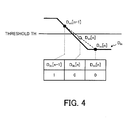
- FIG. 4 is an example of a process performed by each comparison circuit in the second embodiment.
- the first comparison circuit 103 and the second comparison circuit 106 are comparators which perform comparison processes by the use of the same threshold Th.
- the first comparison circuit 103 compares amplitude levels D sc [n ⁇ 1] and D sc [n] inputted in order with the threshold Th and outputs bit values indicative of comparison results.
- the amplitude level D sc [n ⁇ 1] is higher than the threshold Th, so the first comparison circuit 103 outputs the bit value “1” as a comparison result D dc [n ⁇ 1] on the amplitude level D sc [n ⁇ 1].
- the amplitude level D sc [n] is lower than the threshold Th, so the first comparison circuit 103 outputs the bit value “0” as a comparison result D dc [n] on the amplitude level D sc [n].
- the second comparison circuit 106 compares an intermediate level D se [n] with the threshold Th and outputs a bit value indicative of a comparison result.
- the intermediate level D se [n] is lower than the threshold Th, so the second comparison circuit 106 outputs the bit value “0” as a comparison result D de [n] on the intermediate level D se [n].
- the first comparison circuit 103 and the second comparison circuit 106 compare inputted amplitude levels D sc and an intermediate level D se , respectively, with the threshold Th and output bit values indicative of comparison results.
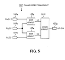
- FIG. 5 is an example of the phase detection circuit in the second embodiment.
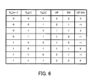
- FIG. 6 indicates the relationships among inputs to and an output from the phase detection circuit in the second embodiment.
- the phase detection circuit 107 includes XOR (exclusive disjunction) circuits 107 d and 107 e and a logic circuit 107 f .
- One input of the XOR circuit 107 d is connected to an input terminal 107 a and the other input of the XOR circuit 107 d is connected to an input terminal 107 b .
- An output of the XOR circuit 107 d is connected to an input of the logic circuit 107 f .
- One input of the XOR circuit 107 e is connected to the input terminal 107 b and the other input of the XOR circuit 107 e is connected to an input terminal 107 c .
- An output of the XOR circuit 107 e is connected to an input of the logic circuit 107 f .
- An output of the logic circuit 107 f is connected to an output terminal 107 g.
- amplitude levels D dc [n ⁇ 1], D de [n], and D dc [n] are inputted to the input terminal 107 a , 107 b , and 107 c respectively.
- an output from the XOR circuit 107 d is indicated by “UP” and an output from the XOR circuit 107 e is indicated by “DN”.
- the relationships among D dc [n ⁇ 1], D de [n], D dc [n], UP, and DN are given by a table indicated in FIG. 6 .
- the logic circuit 107 f outputs an UP/DN signal on the basis of a combination of UP and DN.
- the logic circuit 107 f holds in a look-up table the relationships among UP, DN, and an UP/DN signal indicated in FIG. 6 , refers to the look-up table, and outputs a value of UP/DN according to inputted UP and DN. For example, if D dc [n ⁇ 1] is “0”, D de [n] is “0”, and D dc [n] is “1”, UP is “0” and DN is “1”.
- the logic circuit 107 f outputs an UP/DN signal ( ⁇ 1) corresponding to a case where (UP, DN) is (0, 1).
- the UP/DN signal ( ⁇ 1) indicates that a phase of a sampling clock is fast. Accordingly, an adjustment is made at a subsequent stage for setting back a phase of the sampling clock.
- the logic circuit 107 f outputs an UP/DN signal (+1) corresponding to a case where (UP, DN) is (1, 0).
- the UP/DN signal (+1) indicates that a phase of the sampling clock is slow. Accordingly, an adjustment is made at a subsequent stage for setting forward a phase of the sampling clock.
- an UP/DN signal indicative of a phase deviation of the sampling clock is outputted for the other combinations.
- An UP/DN signal the value of which is is outputted for a combination by which a phase deviation of the sampling clock is not be detected.
- phase detection circuit 107 in the second embodiment has been described.
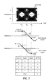
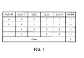
- FIG. 7 is an example of a 4-bit pattern filter in the second embodiment.
- the phase detection circuit 107 can detect a phase deviation of the sampling clock by the use of the three bit values D dc [n ⁇ 1], D de [n], and D dc [n] on the basis of the above method.
- a phase detection circuit 107 in the modification decides whether or not a pattern obtained by combining the four bit values D dc [n ⁇ 2], D dc [n ⁇ 1], D dc [n], and D dc [n+1] matches a determined filter pattern. If a pattern obtained by combining the four bit values D dc [n ⁇ 2], D dc [n ⁇ 1], D dc [n], and D dc [n+1] matches a determined filter pattern, then the phase detection circuit 107 outputs an UP/DN signal corresponding to a detected phase deviation.
- the phase detection circuit 107 outputs an UP/DN signal the value of which is “0”.
- the patterns (0011) and (1100) are set as filter patterns. If a great loss occurs, the influence of inter-symbol interference increases and, therefore, the amplitude of a high-frequency component of the input data signal D in becomes small. With the patterns (0101), (1010), and the like, a slew rate is very low. That is to say, signal-to-noise ratio at a zero-crossing point deteriorates and phase deviation detection accuracy deteriorates. Accordingly, the exclusion of these patterns prevents phase deviation detection accuracy from deteriorating. In addition, the exclusion of the patterns (0010), (0100), and the like in which only one bit is “1” or “0” prevents phase deviation detection accuracy further from deteriorating.
- a mechanism in which a large number of filter patters are applied in the case of a slew rate of the input data signal D in being lower than a determined threshold and in which a small number of filter patters are applied in the other cases may be adopted.
- a mechanism in which a large number of filter patters are applied in the case of an interval between sampling timings corresponding to two threshold levels used for calculating an intermediate level being short and in which a small number of filter patters are applied in the other cases may be adopted.
- a mechanism in which a filter pattern is not applied instead of applying a small number of filter patters may be adopted.
- the modification in the second embodiment has been described.
- the accuracy with which a phase deviation of the sampling clock is detected hardly deteriorates even if, for example, a great loss occurs.
- a method for setting a filter pattern by combining four bit values is indicated.
- a method for setting a filter pattern by combining three bit values may be applied.
- the second embodiment has been described.
- a third embodiment will now be described.
- the method of replacing a comparison circuit which detects a bit value for data detection with a DFE is proposed.
- a mechanism in which signal loss and a slew rate are estimated from an equalization coefficient of the DFE and in which a filter pattern is switched according to an estimation result is proposed.
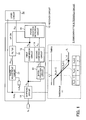
- FIG. 8 is an example of a receiver circuit according to a third embodiment.
- the receiver circuit 200 includes a data input terminal 201 , a sampling circuit 202 , an equalizer 203 , an adaptive logic circuit 204 , and a data output terminal 205 .
- the receiver circuit 200 includes a data interpolation circuit 206 , a comparison circuit 207 , a phase detection circuit 208 , a filter 209 , a phase adjustment circuit 210 , and a clock input terminal 211 .
- the data input terminal 201 , the sampling circuit 202 , and the data output terminal 205 are substantially the same as the data input terminal 101 , the sampling circuit 102 , and the data output terminal 104 , respectively, in the second embodiment. Furthermore, the data interpolation circuit 206 , the comparison circuit 207 , the filter 209 , the phase adjustment circuit 210 , and the clock input terminal 211 are substantially the same as the data interpolation circuit 105 , the second comparison circuit 106 , the filter 108 , the phase adjustment circuit 109 , and the clock input terminal 110 , respectively, in the second embodiment. Accordingly, detailed description of these components will be omitted.
- An input data signal D in is inputted to the data input terminal 201 .
- the input data signal D in is inputted to the sampling circuit 202 .
- the sampling circuit 202 detects an amplitude level D sc of the input data signal D in at a sampling timing indicated by a sampling clock CLK s .
- the amplitude level D sc detected by the sampling circuit 202 is inputted to the equalizer 203 , the adaptive logic circuit 204 , and the data interpolation circuit 206 .
- the equalizer 203 removes inter-symbol interference between a bit decided in the past and a bit which is to be decided by feeding back a decided signal and performing weighting synthesis.
- a decision feedback equalizer DFE
- another adaptive linear equalizer or nonlinear equalizer such as an MLSE (Maximum Likelihood Sequence Estimator)
- the equalizer 203 performs an equalization process on the amplitude level D sc by the use of an equalization coefficient C DFE and outputs a bit value D dc indicative of a result obtained by comparing a signal after equalization and a determined threshold Th.
- a circuit and the operation of the equalizer 203 will be described later in detail.
- the bit value D dc outputted from the equalizer 203 is outputted as received data D out from the data output terminal 205 to the outside of the receiver circuit 200 .
- the bit value D dc is inputted to the adaptive logic circuit 204 and the phase detection circuit 208 .
- the adaptive logic circuit 204 exercises control so that the equalization coefficient C DFE (combination of equalization coefficients w 1 , w 2 , and so on described later) used by the equalizer 203 for performing an equalization process will be an optimum value.
- the equalization coefficient C DFE is calculated by the use of an optimization algorithm such as an LMS (Least Mean Square) algorithm or an RLS (Recursive Least Square) algorithm.
- the adaptive logic circuit 204 estimates loss in the amplitude level D sc or a slew rate from the value of the equalization coefficient C DFE and outputs a data pattern code C DP corresponding to the magnitude of the loss in the amplitude level D sc or the value of the slew rate.
- the data pattern code C DP is inputted to the phase detection circuit 208 .
- the method of detecting the difference between an amplitude level D sc obtained in the case of bit values D dc being (1111111) and an amplitude level D sc corresponding to the bit value D dc “1” in the case of bit values D dc being (0001000) may be used as a loss estimation method.
- This difference is the difference between a low-frequency component and a high-frequency component of the input data signal D in . As loss increases, this difference grows. Accordingly, by detecting this difference, loss can be estimated.
- the method of estimating a slew rate from an amplitude level D sc corresponding to each bit value D dc in the case of bit values D dc being (000111) may be used as a slew rate estimation method.
- the following method may be used.
- the data interpolation circuit 206 performs an interpolation process by the use of two amplitude levels D sc detected at two sampling timings to find an intermediate level D se which approximates to an amplitude level of the input data signal D in at a zero-crossing point.
- the intermediate level D se found by the data interpolation circuit 206 is inputted to the comparison circuit 207 .
- the comparison circuit 207 compares the intermediate level D se inputted from the data interpolation circuit 206 with a determined threshold Th. If the intermediate level D se is higher than the determined threshold Th, then the comparison circuit 207 outputs the bit value “1” as a comparison result D de . If the intermediate level D se is lower than the determined threshold Th, then the comparison circuit 207 outputs the bit value “0” as a comparison result D de .
- the bit value D de indicative of a comparison result is inputted to the phase detection circuit 208 .
- the phase detection circuit 208 detects a phase deviation of a sampling clock on the basis of the bit value D dc inputted from the equalizer 203 and the bit value D de inputted from the comparison circuit 207 , and outputs an UP/DN signal indicative of a detection result. At this time the phase detection circuit 208 outputs an UP/DN signal with a filter pattern taken into consideration. This is the same with the modification in the second embodiment. At this time the phase detection circuit 208 switches the contents of a filter pattern according to the data pattern code C DP inputted from the adaptive logic circuit 204 . A method for switching a filter pattern will be described later in detail.
- the UP/DN signal outputted from the phase detection circuit 208 is inputted to the filter 209 .
- the filter 209 outputs a phase code Ph code obtained by removing a high-frequency component of the UP/DN signal inputted from the phase detection circuit 208 .
- the phase code Ph code is inputted to the phase adjustment circuit 210 .
- a clock CLK in before phase adjustment is inputted from the clock input terminal 211 to the phase adjustment circuit 210 .
- the phase adjustment circuit 210 adjusts a phase of the clock CLK in in accordance with the phase code Ph code and outputs a sampling clock CLK s .
- the sampling clock CLK s after phase adjustment is inputted to the sampling circuit 202 .
- the receiver circuit 200 according to the third embodiment differs from the receiver circuit 100 according to the second embodiment in the equalizer 203 , the adaptive logic circuit 204 , and the phase detection circuit 208 .
- the equalizer 203 , the adaptive logic circuit 204 , and the phase detection circuit 208 will now be described further.
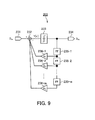
- FIG. 9 is an example of the equalizer (m-tap DFE) in the third embodiment.
- the equalizer 203 includes an adder and subtractor 232 , a comparison circuit 233 , a flip-flop circuit 235 ( 235 - 1 through 235 - m ), and a buffer circuit 236 ( 236 - 1 through 236 - m ). It is assumed that equalization coefficients w 1 , . . . , and w m are given to the buffer circuits 236 - 1 through 236 - m respectively. These equalization coefficients w 1 , . . . , and w m are equalization coefficients C DFE supplied from the adaptive logic circuit 204 . In addition, a threshold Th used by the comparison circuit 233 is the same as the threshold Th used by the comparison circuit 207 .
- An amplitude level D sc outputted from the sampling circuit 202 is inputted to an input terminal 231 .
- the adder and subtractor 232 subtracts values outputted from the buffer circuits 236 - 1 through 236 - m from the amplitude level D sc inputted via the input terminal 231 , and outputs a signal Y.
- the signal Y is inputted to the comparison circuit 233 .
- the comparison circuit 233 compares the signal Y and the threshold Th and outputs a bit value D dc indicative of a comparison result.
- the bit value D dc is outputted via an output terminal 234 and is inputted to the adaptive logic circuit 204 , the data output terminal 205 , and the phase detection circuit 208 .
- bit value D dc is inputted to the flip-flop circuit 235 - 1 .
- the flip-flop circuit 235 - 1 holds the bit value D dc only for one interval until the next bit value is inputted. After that, the flip-flop circuit 235 - 1 outputs the bit value D dc .
- the bit value D dc outputted from the flip-flop circuit 235 - 1 is inputted to the buffer circuit 236 - 1 and the flip-flop circuit 235 - 2 .
- the buffer circuit 236 - 1 multiplies the bit value D dc and the equalization coefficient w 1 together and inputs a value obtained by the multiplication to the adder and subtractor 232 .
- the flip-flop circuits 235 - 2 through 235 - m operate the same as the flip-flop circuit 235 - 1 .
- the buffer circuits 236 - 2 through 236 - m use the corresponding equalization coefficients w 2 through w m , respectively, and operate the same as the buffer circuit 236 - 1 .
- an amplitude level D sc [n] sampled in interval n (n>m) is inputted to the input terminal 231 .
- the buffer circuit 236 - 1 multiplies a bit value D dc [n ⁇ 1] held by the flip-flop circuit 235 - 1 and the equalization coefficient w 1 together and inputs a value w 1 *D dc [n ⁇ 1] to the adder and subtractor 232 .
- w 2 *D dc [n ⁇ 2], . . . , and w m *D dc [n ⁇ m] are inputted to the adder and subtractor 232 . Accordingly, a signal Y[n] outputted from the adder and subtractor 232 is given by
- the comparison circuit 233 compares the signal Y[n] and the threshold Th and outputs a bit value D dc [n] indicative of a comparison result.
- the bit value D dc [n] is outputted from the output terminal 234 and is held by the flip-flop circuit 235 - 1 .
- the flip-flop circuits 235 - 2 through 235 - m hold bit values D dc [n ⁇ 1] through D dc [n ⁇ m ⁇ 1] respectively.
- the bit value D dc [n] outputted from the output terminal 234 is inputted to the adaptive logic circuit 204 and is used for updating the equalization coefficients w 1 through w m . If the LMS algorithm, for example, is applied, the equalization coefficients w 1 through w m are updated in accordance with:
- q is a step size parameter.
- a step size q is set to, for example, about 0.01 to 0.001.
- the adaptive logic circuit 204 uses the bit value D dc [n] inputted from the equalizer 203 for sequentially updating the equalization coefficients w 1 through w m .
- the adaptive logic circuit 204 then supplies the equalization coefficients w 1 through w m after the update to the equalizer 203 as an equalization coefficient C DFE . By repeating such an update, the equalization coefficients w 1 through w m converge at optimum values.
- FIG. 10 is an example of the equalizer (1-tap speculative DFE) in the third embodiment.
- a speculative DFE acquires both the past data “0” and the past data “1” as decided data, and selects, after the settlement of the past data, a correct value on the basis of the past data. Accordingly, a speculative DFE can perform high-speed operation.
- an equalizer 203 includes comparison circuits 253 and 254 , a selector 255 , and a flip-flop circuit 257 .
- An equalization coefficient w 1 is inputted from an input terminal 252 to the comparison circuits 253 and 254 .
- the comparison circuit 253 compares a threshold Th 1 obtained by shifting a threshold Th by +w 1 and an amplitude level D sc inputted from an input terminal 251 .
- the comparison circuit 254 compares a threshold Th 2 obtained by shifting the threshold Th by ⁇ w 1 and the amplitude level D sc inputted from the input terminal 251 .
- a bit value D dc1 indicative of a result of the comparison made by the comparison circuit 253 and a bit value D dc2 indicative of a result of the comparison made by the comparison circuit 254 are inputted to the selector 255 .
- bit value D dc corresponding to an amplitude level D sc obtained at the preceding sampling timing is “1”
- the selector 255 selects the bit value D dc1 .
- the selector 255 selects the bit value D dc2 .
- the selector 255 then outputs a selected bit value as a bit value D dc indicative of a decision result.
- the bit value D dc outputted from the selector 255 is outputted from an output terminal 256 and is held by the flip-flop circuit 257 .
- the bit value D dc held by the flip-flop circuit 257 is used when the selector 255 selects a bit value at the next timing.
- bit value D dc1 [n] is outputted from the comparison circuit 253 and a bit value D dc2 [n] is outputted from the comparison circuit 254 .
- bit values D dc1 [n] and D dc2 [n] are inputted to the selector 255 .
- a bit value D dc [n ⁇ 1] held by the flip-flop circuit 257 is inputted to the selector 255 .
- bit value D dc [n ⁇ 1] is “1”
- the selector 255 outputs the bit value D dc1 [n] as a bit value D dc [n].
- the selector 255 outputs the bit value D dc2 [n] as a bit value D dc [n].
- the bit value D dc [n] outputted from the selector 255 is outputted from the output terminal 256 and is held by the flip-flop circuit 257 .
- the bit value D dc [n] outputted from the output terminal 256 is outputted from the data output terminal 205 to the outside and is inputted to the adaptive logic circuit 204 and the phase detection circuit 208 .
- the adaptive logic circuit 204 updates the equalization coefficient w 1 on the basis of the inputted bit value D dc [n].
- An update method is the same with the m-tap DFE.
- the adaptive logic circuit 204 updates every bit the equalization coefficients w 1 through w m used by the equalizer 203 for performing an equalization process. If there is a great loss in an amplitude level D sc , the values of the equalization coefficients w 1 through w m will be high. Furthermore, if a slew rate indicative of the slope of a rising or falling edge of an input data signal D in is high, the values of the equalization coefficients w 1 through w m will be high.
- the adaptive logic circuit 204 generates the data pattern code C DP indicative of the magnitude of loss in amplitude level D sc or the value of a slew rate on the basis of the values of the equalization coefficients w 1 through w m .
- the adaptive logic circuit 204 considers a value obtained by simply adding together the equalization coefficients w 1 through w m as the data pattern code C DP .
- the adaptive logic circuit 204 may consider the sum of the absolute values of the equalization coefficients w 1 through w m (
- the adaptive logic circuit 204 may consider the sum of the squares of the equalization coefficients w 1 through w m (w 1 2 + . . . +w m 2 ) as the data pattern code C DP .
- the data pattern code C DP generated in this way is inputted to the phase detection circuit 208 and is used for filter pattern switching.
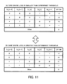
- FIG. 11 indicates a filter pattern switching method in the third embodiment.
- the phase detection circuit 208 uses four amplitude levels and an intermediate level for detecting a phase deviation of a sampling clock. At this time the phase detection circuit 208 decides whether or not a combination of the four amplitude levels matches a filter pattern. If a combination of the four amplitude levels matches a filter pattern, then the phase detection circuit 208 outputs an UP/DN signal the value of which is “0”. That is to say, if a combination of the four amplitude levels matches a filter pattern, the phase detection circuit 208 does not adjust a phase of the sampling clock.
- the phase detection circuit 208 performs filter pattern switching on the basis of the data pattern code C DP inputted from the adaptive logic circuit 204 .
- the phase detection circuit 208 may perform switching on the basis of the data pattern code C DP between filter patterns included in table (A) of FIG. 11 and filter patterns included in table (B) of FIG. 11 .
- the filter patterns included in table (A) are applied if loss indicated by the data pattern code C DP is smaller than a determined threshold.
- “*” in table (A) means “0” and “1”. That is to say, if a filter pattern included in table (A) is applied, filtering is performed by the use of three bit values except a bit value corresponding to “*”.
- a filter pattern included in table (B) is applied if loss indicated by the data pattern code C DP is greater than the determined threshold.
- the filter patterns included in table (B) are the same as those indicated in FIG. 7 .
- filter pattern switching is also performed. For example, the magnitude of loss is determined in the following way.
- the data pattern code C DP and a determined value are compared. If the data pattern code C DP is greater than the determined value, then the determination that a great loss has occurred is made. If the data pattern code C DP is smaller than the determined value, then the determination that a small loss has occurred is made.
- the filter pattern switching method in the third embodiment has been described.
- the following mechanism may be adopted as a modification. If loss is smaller than a determined threshold, switching is performed so that no filter pattern will be applied. Furthermore, the following mechanism may be adopted as a modification. Staged filter pattern switching is performed according to the magnitude of loss in the order of application of a filter pattern included in table (B), a filter pattern included in table (A), and no filter pattern.
- the third embodiment has been described.
- a fourth embodiment will now be described.
- the following mechanism is proposed.
- a part of the receiver circuit according to the second or third embodiment is provided in plurality and parallel connections are made. By doing so, data processing is performed on a plurality of bits in parallel.
- a group of circuits connected in parallel operate intermittently (interleaved operation) in a cycle which is longer than a cycle of a clock CLK in inputted for sampling. This makes it possible to reduce the operating speeds of individual circuits. As a result, it is easy to make a receiver circuit operate at a high data rate.
- FIG. 12 is a first example of a receiver circuit according to the fourth embodiment.
- There are components in a receiver circuit 300 a which have substantially the same functions as the components in the receiver circuit 100 according to the second embodiment have. It may be that only the correspondences between these components in the receiver circuit 300 a and the components in the receiver circuit 100 will be indicated and that detailed description of these components in the receiver circuit 300 a will be omitted.
- the receiver circuit 300 a includes a data input terminal 301 , an amplifier 302 , sampling circuits 303 a through 303 d , first comparison circuits 304 a through 304 d , and data output terminals 305 a through 305 d .
- the receiver circuit 300 a includes data interpolation circuits 306 a through 306 d , second comparison circuits 307 a through 307 d , a phase detection circuit 308 , a filter 309 , a phase adjustment circuit 310 , and a clock input terminal 311 .
- the data input terminal 301 , the sampling circuits 303 a through 303 d , the first comparison circuits 304 a through 304 d , and the data output terminals 305 a through 305 d correspond to the data input terminal 101 , the sampling circuit 102 , the first comparison circuit 103 , and the data output terminal 104 respectively.
- the data interpolation circuits 306 a through 306 d , the second comparison circuits 307 a through 307 d , the phase detection circuit 308 , the filter 309 , the phase adjustment circuit 310 , and the clock input terminal 311 correspond to the data interpolation circuit 105 , the second comparison circuit 106 , the phase detection circuit 107 , the filter 108 , the phase adjustment circuit 109 , and the clock input terminal 110 respectively.
- the receiver circuit 300 a according to the fourth embodiment mainly differs from the receiver circuit 100 according to the second embodiment in timing at which the sampling circuits 303 a through 303 d perform sampling and timing at which each circuit operates according to the timing. Accordingly, description will be given with attention paid to the operation of the sampling circuits 303 a through 303 d and the data interpolation circuits 306 a through 306 d .
- the receiver circuit 300 a according to the fourth embodiment also differs from the receiver circuit 100 according to the second embodiment in that an input data signal D in is amplified by the amplifier 302 .
- the sampling circuit 303 a outputs amplitude levels D sc [n], D sc [n+4], and so on by sampling.
- the sampling circuit 303 b outputs amplitude levels D sc [n+1], D sc [n+5], and so on by sampling.
- the sampling circuit 303 c outputs amplitude levels D sc [n+2], D sc [n+6], and so on by sampling.
- the sampling circuit 303 d outputs amplitude levels D sc [n+3], D sc [n+7], and so on by sampling.
- the sampling circuits 303 a through 303 d operate in a sampling cycle four times the sampling cycle of the sampling circuit 102 in the second embodiment. Furthermore, the data interpolation circuits 306 a through 306 d operate on the basis of data outputted from the sampling circuits 303 a through 303 d respectively, so the data interpolation circuits 306 a through 306 d operate at an operating speed one fourth of an operating speed of the data interpolation circuit 105 in the second embodiment. The same applies to the first comparison circuits 304 a through 304 d and the second comparison circuits 307 a through 307 d . However, the operation of the phase detection circuit 308 and the filter 309 is the same as that of the phase detection circuit 107 and the filter 108 , respectively, in the second embodiment.
- the phase adjustment circuit 310 generates four sampling clocks CLK s1 through CLK s4 which differ in phase from the clock CLK in inputted, and supplies the four sampling clocks CLK s1 through CLK s4 to the sampling circuits 303 a through 303 d respectively. It is assumed that the wavelength of the clock CLK in is ⁇ . Then the wavelengths of the sampling clocks CLK s1 through CLK s4 are 4 ⁇ and their phases differ by ⁇ /2 from one another.
- the phase adjustment circuit 310 adjusts a phase of the clock CLK in on the basis of a phase code Ph code , generates the sampling clocks CLK s1 through CLK s4 from the clock CLK in after the adjustment, and supplies the sampling clocks CLK s1 through CLK s4 to the sampling circuits 303 a through 303 d respectively.
- the receiver circuit 300 a has been described. With the receiver circuit 300 a a group of circuits connected in parallel perform interleaved operation. Accordingly, the operating speeds of individual circuits can be reduced and it is easy to make the receiver circuit 300 a operate at a high data rate. Examples of the sampling circuits 303 a through 303 d and the data interpolation circuits 306 a through 306 d will now be described further.
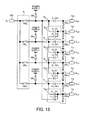
- FIG. 13 illustrates examples of the sampling circuits and the data interpolation circuits in the fourth embodiment.
- a circuit illustrated in FIG. 13 is realized by combining the sampling circuits 303 a through 303 d and the data interpolation circuits 306 a through 306 d . Combining the sampling circuits 303 a through 303 d and the data interpolation circuits 306 a through 306 d in the way illustrated in FIG. 13 makes the area of the circuit small. A portion in FIG. 13 which is marked with the letter “a” and which is enclosed by a dashed line corresponds to the sampling circuits 303 a through 303 d .
- portions which are marked with the numerals b 01 , b 12 , b 23 , and b 30 and which are enclosed by dashed lines correspond to holding sections in the data interpolation circuits 306 a through 306 d for holding an amplitude level D sc and main sections of circuits in the data interpolation circuits 306 a through 306 d for finding an intermediate level D se .
- the circuit illustrated in FIG. 13 includes switches SW s0 , SW s1 , SW s2 , SW s3 , SW h0 , SW h1 , SW h2 , SW h3 , SW r00 , SW r10 , SW r11 , SW r20 , SW r21 , SW r30 , SW r31 , and SW r01 and capacitances C 1 through C 12 .
- the switches SW s0 , SW s1 , SW s2 , and SW s3 are sampling switches.
- the switches SW h0 , SW h1 , SW h2 , and SW h3 are holding switches.
- the switches SW r00 , SW r01 , SW r10 , SW r11 , SW r20 , SW r21 , SW r30 , and SW r31 are resetting switches.
- the switch SW r00 is interlocked with the switch SW r01 .
- the switch SW r10 is interlocked with the switch SW r11 .
- the switch SW r20 is interlocked with the switch SW r21 .
- the switch SW r30 is interlocked with the switch SW r31 .
- switches SW r00 and SW r01 , the switches SW r10 and SW r11 , the switches SW r20 and SW r21 , and the switches SW r30 and SW r31 may be represented in block as switches SW r0 , SW r1 , SW r2 , and SW r3 respectively.
- the values of the capacitances C 1 , C 4 , C 7 , and C 10 are set to 2C (C is a determined value) and the values of the capacitances C 2 , C 3 , C 5 , C 6 , C 8 , C 9 , C 11 , and C 12 are set to C. That is to say, the values of the capacitances C 1 , C 4 , C 7 , and C 10 are twice the values of the capacitances C 2 , C 3 , C 5 , C 6 , C 8 , C 9 , C 11 , and C 12 .
- each of the switches SW s0 , SW s1 , SW s2 , and SW s3 is connected to a data input terminal 301 .
- the other end of the switch SW s0 is connected to a node N 0 .
- the other end of the switch SW s1 is connected to a node N 1 .
- the other end of the switch SW s2 is connected to a node N 2 .
- the other end of the switch SW s3 is connected to a node N 3 .
- one end of each of the switches SW h0 , SW h1 , SW h2 , and SW h3 is connected to power supply which supplies determined voltage.
- the other end of the switch SW h0 is connected to the node N 0 .
- the other end of the switch SW h1 is connected to the node N 1 .
- the other end of the switch SW h2 is connected to the node N 2 .
- the other end of the switch SW h3 is connected to the node N 3 .
- one end of each of the switches SW r00 , SW r10 , SW r11 , SW r20 , SW r21 , SW r30 , SW r31 , and SW r01 is grounded.
- the other end of the switch SW r00 is connected to an output terminal c 00 .
- the other end of the switch SW r10 is connected to an output terminal c 01 .
- the other end of the switch SW r11 is connected to an output terminal c 10 .
- the other end of the switch SW r20 is connected to an output terminal c 11 .
- the other end of the switch SW r21 is connected to an output terminal c 20 .
- the other end of the switch SW r30 is connected to an output terminal c 21 .
- the other end of the switch SW r31 is connected to an output terminal c 30 .
- the other end of the switch SW r01 is connected to an output terminal c 31 .
- One end of the capacitance C 1 is connected to the node N 0 .
- One end of the capacitance C 4 is connected to the node N 1 .
- One end of the capacitance C 7 is connected to the node N 2 .
- One end of the capacitance C 10 is connected to the node N 3 .
- the other end of the capacitance C 1 is connected to the output terminal c 00 .
- the other end of the capacitance C 4 is connected to the output terminal c 10 .
- the other end of the capacitance C 7 is connected to the output terminal c 20 .
- the other end of the capacitance C 10 is connected to the output terminal c 30 .
- one end of the capacitance C 2 is connected to the node N 0 .
- One end of the capacitance C 5 is connected to the node N 1 .
- One end of the capacitance C 8 is connected to the node N 2 .
- One end of the capacitance C 11 is connected to the node N 3 .
- the other end of the capacitance C 2 is connected to the output terminal c 01 .
- the other end of the capacitance C 5 is connected to the output terminal c 11 .
- the other end of the capacitance C 8 is connected to the output terminal c 21 .
- the other end of the capacitance C 11 is connected to the output terminal c 31 .
- one end of the capacitance C 3 is connected to the node N 1 .
- One end of the capacitance C 6 is connected to the node N 2 .
- One end of the capacitance C 9 is connected to the node N 3 .
- One end of the capacitance C 12 is connected to the node N 0 .
- the other end of the capacitance C 3 is connected to the output terminal c 01 .
- the other end of the capacitance C 6 is connected to the output terminal c 11 .
- the other end of the capacitance C 9 is connected to the output terminal c 21 .
- the other end of the capacitance C 12 is connected to the output terminal c 31 .
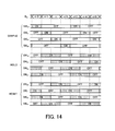
- FIG. 14 indicates operation timing of each switch included in the sampling circuits and the data interpolation circuits in the fourth embodiment.
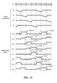
- FIG. 15 indicates a change in node potential and a change in outputted amplitude level in the sampling circuits and the data interpolation circuits in the fourth embodiment.
- each switch in intervals corresponding to (n ⁇ 2)th through (n+5)th bits of an input data signal D in is indicated.
- the sampling switch SW s0 is in an on state in the interval (n ⁇ 2).
- the holding switch SW h0 is in an off state and the resetting switch SW r0 is in an off state.
- the switch SW s0 is turned on, electric charges are drawn out of the capacitances C 1 , C 2 , and C 12 connected to the switch SW s0 by an amount corresponding to an amplitude level of the input data signal D in , and the potential of the node N 0 falls (see node potential (N 0 ) in FIG. 15 ).
- the value of the capacitance C 1 is twice the values of the capacitances C 2 and C 12 , so the amount of electric charges drawn out of the capacitances C 2 and C 12 is half of the amount of electric charges drawn out of the capacitance C 1 .
- the sampling switch SW s0 is in an off state in the interval (n ⁇ 1).
- the holding switch SW h0 is in an on state in the interval (n ⁇ 1).
- the switch SW h0 is turned on, power is supplied from the power supply connected to the switch SW h0 and the potential of the node N 0 rises (see node potential (N 0 ) in FIG. 15 ).
- the potential of the output terminal c 00 rises by the amount of electric charges drawn out of the capacitance C 1 in the interval (n ⁇ 2) (see amplitude level (D sc0 ) in FIG. 15 ).
- the amount of this rise in potential is a sampled amplitude level D sc [n ⁇ 2] of the input data signal D in .
- the potential of the output terminal c 01 also rises by the amount of electric charges drawn out of the capacitance C 2 in the interval (n ⁇ 2).
- the sampling switch SW s1 is in an on state in the interval (n ⁇ 1). At this time the holding switch SW h1 is in an off state and the resetting switch SW r1 is in an off state.
- the switch SW s1 is turned on, electric charges are drawn out of the capacitances C 3 , C 4 , and c 5 connected to the switch SW s1 by an amount corresponding to an amplitude level of the input data signal D in , and the potential of the node N 1 falls (see node potential (N 1 ) in FIG. 15 ).
- the value of the capacitance C 4 is twice the values of the capacitances C 3 and C 5 , so the amount of electric charges drawn out of the capacitances C 3 and C 5 is half of the amount of electric charges drawn out of the capacitance C 4 .
- the sampling switch SW s1 is in an off state in the interval n.
- the holding switch SW h1 is in an on state in the interval n.
- the switch SW h1 When the switch SW h1 is turned on, power is supplied from the power supply connected to the switch SW h1 and the potential of the node N 1 rises (see node potential (N 1 ) in FIG. 15 ).
- the potential of the output terminal c 10 rises by the amount of electric charges drawn out of the capacitance C 4 in the interval (n ⁇ 1) (see amplitude level (D sc1 ) in FIG. 15 ).
- the amount of this rise in potential is a sampled amplitude level D sc [n ⁇ 1] of the input data signal D in .
- the potential of the output terminal c 01 rises further in the interval n by the amount of electric charges drawn out of the capacitance C 3 in the interval (n ⁇ 1).
- the holding switch SW h0 also remains in an on state, so the potential of the output terminal c 01 rises by an amount of electric charges obtained by adding together the amount of electric charges drawn out of the capacitance C 2 in the interval (n ⁇ 2) and the amount of electric charges drawn out of the capacitance C 3 in the interval (n ⁇ 1). That is to say, a rise in potential corresponding to a value intermediate between the two amplitude levels D sc0 and D sc1 takes place at the output terminal c 01 (see amplitude level (D se0 ) in FIG. 15 ). The amount of this rise in potential is an intermediate level D se [n ⁇ 2].
- the resetting switches SW r0 (SW r00 and SW r01 ) are in an on state in the interval n and electric charges drawn out of the capacitance C 1 (and c 12 ) are reset. Furthermore, the resetting switches SW r1 (SW r10 and SW r11 ) are in an on state in the interval (n+1) and electric charges drawn out of the capacitances C 2 , C 3 , and C 4 are reset. Circuit operations for finding the two amplitude levels D sc [n ⁇ 2] and D sc [n ⁇ 1] and the intermediate level D se [n ⁇ 2] have been described. By making each switch operate at a timing indicated in FIG. 14 , an amplitude level D sc in each interval and an intermediate level D se are obtained in order.
- sampling circuits 303 a through 303 d and the data interpolation circuits 306 a through 306 d in the fourth embodiment have been described.
- the circuit illustrated in FIG. 13 and making each switch operate at a timing indicated in FIG. 14 the sampling of the input data signal D in and an interpolation process can be realized by the circuit having a small area.
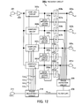
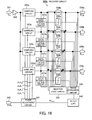
- FIG. 16 is a second example of the receiver circuit according to the fourth embodiment.
- the receiver circuit 300 b includes a data input terminal 331 , an amplifier 332 , sampling circuits 333 a through 333 d , equalizers 334 a through 334 d , an adaptive logic circuit 335 , and data output terminals 336 a through 336 d .
- the receiver circuit 300 b includes data interpolation circuits 337 a through 337 d , comparison circuits 338 a through 338 d , a phase detection circuit 339 , a filter 340 , a phase adjustment circuit 341 , and a clock input terminal 342 .
- the data input terminal 331 , the sampling circuits 333 a through 333 d , and the equalizers 334 a through 334 d are substantially the same as the data input terminal 201 , the sampling circuit 202 , and the equalizer 203 , respectively, in the third embodiment.
- the adaptive logic circuit 335 and the data output terminals 336 a through 336 d are substantially the same as the adaptive logic circuit 204 and the data output terminal 205 , respectively, in the third embodiment.
- the data interpolation circuits 337 a through 337 d , the comparison circuits 338 a through 338 d , and the phase detection circuit 339 are substantially the same as the data interpolation circuit 206 , the comparison circuit 207 , and the phase detection circuit 208 , respectively, in the third embodiment.
- the filter 340 , the phase adjustment circuit 341 , and the clock input terminal 342 are substantially the same as the filter 209 , the phase adjustment circuit 210 , and the clock input terminal 211 , respectively, in the third embodiment.
- sampling clocks CLK s1 through CLK s4 supplied from the phase adjustment circuit 341 are the same as the sampling clocks CLK s1 through CLK s4 , respectively, supplied from the phase adjustment circuit 310 included in the receiver circuit 300 a.
- the components included in the receiver circuit 300 b have substantially the same functions as the components included in the receiver circuit 200 according to the third embodiment have.
- a mechanism by which interleaved operation by the receiver circuit 300 b is realized is substantially the same with the above receiver circuit 300 a . Accordingly, detailed description of each component included in the receiver circuit 300 b will be omitted.
- the receiver circuit 300 b according to the fourth embodiment has been described.
- the sampling circuits 333 a through 333 d and the data interpolation circuits 337 a through 337 d can be realized by the circuit which has already been described with reference to FIGS. 13 through 15 . If this circuit is adopted, a group of circuits connected in parallel perform interleaved operation. Therefore, the operating speeds of individual circuits can be reduced and the receiver circuit 300 b operates easily at a high data rate.
- the fourth embodiment has been described.
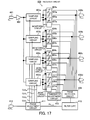
- FIG. 17 is an example of a receiver circuit including a BR phase detector having an amplitude adjustment function.
- a BR phase detector compares one amplitude level per bit obtained by sampling an input data signal with three thresholds to detect a phase deviation of a sampling clock.
- One of the three thresholds is set to a zero level and the other two thresholds are set to levels above and below the zero level.
- the threshold set to a level above the zero level is indicated by “de+”
- the threshold set to the zero level is indicated by “dc”
- the threshold set to a level below the zero level is indicated by “de ⁇ ”.
- a decision result obtained on the basis of the threshold de+ is indicated by D de+
- a decision result obtained on the basis of the threshold dc is indicated by D dc
- a decision result obtained on the basis of the threshold de ⁇ is indicated by D de ⁇ .
- the BR phase detector decides that a phase of the sampling clock is slow.
- the above combination is (000011) or (111001)
- the BR phase detector decides that a phase of the sampling clock is fast.
- the BR phase detector makes a decision in this way on the basis of the thresholds de+ and de ⁇ set above and below the zero level. Accordingly, variations in the amplitude of an input data signal caused by the influence of transmission line loss, noise, or the like tend to have an influence on a decision result.
- the following method for example, may be adopted.
- the amplitude of an input data signal is detected and a threshold is adjusted according to a detection result.
- a receiver circuit 400 including a BR phase detector having an amplitude adjustment function to which this method is applied is illustrated as an example in FIG. 17 .
- sampling circuits and the like are connected in parallel. This is the same with the above receiver circuits 300 a and 300 b according to the fourth embodiment. Accordingly, the receiver circuit 400 can perform interleaved operation.
- the receiver circuit 400 includes a data input terminal 401 , an amplifier 402 , sampling circuits 403 a through 403 d , first comparison circuits 404 a through 404 d , second comparison circuits 405 a through 405 d , and third comparison circuits 406 a through 406 d .
- the receiver circuit 400 includes monitoring circuits 407 a through 407 d , data output terminals 408 a through 408 d , a phase detection circuit 409 , a filter 410 , a phase adjustment circuit 411 , a clock input terminal 412 , and a threshold adjustment circuit 413 .
- An input data signal D in is inputted to the data input terminal 401 .
- the input data signal D in is amplified by the amplifier 402 and is inputted to the sampling circuits 403 a through 403 d .
- the sampling circuits 403 a through 403 d sample the input data signal D in at sampling timings indicated by sampling clocks CLK s1 through CLK s4 , respectively, supplied from the phase adjustment circuit 441 .
- An amplitude level D s of the input data signal D in sampled by the sampling circuit 403 a is inputted to the first comparison circuit 404 a , the second comparison circuit 405 a , the third comparison circuit 406 a , and the monitoring circuit 407 a .
- An amplitude level D s of the input data signal D in sampled by the sampling circuit 403 b is inputted to the first comparison circuit 404 b , the second comparison circuit 405 b , the third comparison circuit 406 b , and the monitoring circuit 407 b.
- An amplitude level D s of the input data signal D in sampled by the sampling circuit 403 c is inputted to the first comparison circuit 404 c , the second comparison circuit 405 c , the third comparison circuit 406 c , and the monitoring circuit 407 c .
- An amplitude level D s of the input data signal D in sampled by the sampling circuit 403 d is inputted to the first comparison circuit 404 d , the second comparison circuit 405 d , the third comparison circuit 406 d , and the monitoring circuit 407 d.
- the first comparison circuit 404 a compares a first threshold de+ and the amplitude level D s and outputs a bit value D de+ indicative of a comparison result.
- the second comparison circuit 405 a compares a second threshold dc and the amplitude level D s and outputs a bit value D dc indicative of a comparison result.
- the third comparison circuit 406 a compares a third threshold de ⁇ and the amplitude level D s and outputs a bit value D de ⁇ indicative of a comparison result.
- the second threshold dc is set to a zero level
- the first threshold de+ is set a value greater than the second threshold dc
- the third threshold de ⁇ is set a value smaller than the second threshold dc.
- the bit value D de+ outputted from the first comparison circuit 404 a is inputted to the phase detection circuit 409 .
- the bit value D dc outputted from the second comparison circuit 405 a is outputted as received data D out0 from the data output terminal 408 a to the outside of the receiver circuit 400 and is inputted to the phase detection circuit 409 .
- the bit value D de ⁇ outputted from the third comparison circuit 406 a is inputted to the phase detection circuit 409 .
- the monitoring circuit 407 a monitors the amplitude level D s and decides whether or not the amplitude level D s is within a determined range.
- a first range centered at the first threshold de+ and a second range centered at the third threshold de ⁇ are set as the determined range.
- the width of the first range and the second range is set to a value (which is found in advance by experiments, for example) by which a phase deviation of a sampling clock can be detected with determined accuracy or higher on the basis of the bit values D de+ , D dc , and D de ⁇ .
- the width of the first range is set to about several percent of the first threshold de+ and the width of the second range is set to about several percent of the third threshold de ⁇ . If the amplitude level D s deviates from the determined range, then the monitoring circuit 407 a inputs to the threshold adjustment circuit 413 a signal indicative of a direction (upward or downward) in which the deviation occurs and an amount of the deviation. If the amplitude level D s is within the determined range, then the monitoring circuit 407 a inputs to the threshold adjustment circuit 413 a signal which indicates that deviation does not occur.
- the sampling circuits 403 b through 403 d , the first comparison circuits 404 b through 404 d , the second comparison circuits 405 b through 405 d , the third comparison circuits 406 b through 406 d , and the monitoring circuits 407 b through 407 d operate in the same way.
- the first comparison circuits 404 a through 404 d use the same first threshold de+.
- the second comparison circuits 405 a through 405 d use the same second threshold dc.
- the third comparison circuits 406 a through 406 d use the same third threshold de ⁇ .
- the threshold adjustment circuit 413 adjusts the first threshold de+ and the third threshold de ⁇ according to signals inputted from the monitoring circuits 407 a through 407 d . For example, if the amplitude level D s deviates upward from the first range, then the threshold adjustment circuit 413 shifts the first threshold de+ upward on the basis of an amount of the deviation so that the amplitude level D s will be within the first range. In addition, the threshold adjustment circuit 413 shifts the third threshold de ⁇ downward by the same amount that the threshold adjustment circuit 413 shifts the first threshold de+ by.
- the threshold adjustment circuit 413 shifts the first threshold de+ downward on the basis of an amount of the deviation so that the amplitude level D s will be within the first range. In addition, the threshold adjustment circuit 413 shifts the third threshold de ⁇ upward by the same amount that the threshold adjustment circuit 413 shifts the first threshold de+ by.
- the phase detection circuit 409 detects a phase deviation of the sampling clock on the basis of the bit values D de+ , D dc , and D de ⁇ inputted in order from the first comparison circuits 404 a through 404 d , the second comparison circuits 405 a through 405 d , and the third comparison circuits 406 a through 406 d .
- an SSMMPD Sim-Sign Mueller Muller Phase Detector
- the phase detection circuit 409 decides that a phase of the sampling clock is slow. In addition, if the above combination is (000011) or (111001), then the phase detection circuit 409 decides that a phase of the sampling clock is fast. If the phase detection circuit 409 decides that a phase of the sampling clock is slow, then the phase detection circuit 409 outputs an UP/DN signal whose value is “+1”.
- phase detection circuit 409 decides that a phase of the sampling clock is fast, then the phase detection circuit 409 outputs an UP/DN signal whose value is “ ⁇ 1”. In the other cases, the phase detection circuit 409 outputs an UP/DN signal whose value is “0”.
- the UP/DN signal outputted from the phase detection circuit 409 is inputted to the filter 410 .
- the filter 410 removes a high-frequency component from the UP/DN signal and generates and outputs a phase code Ph code .
- the phase code Ph code outputted from the filter 410 is inputted to the phase adjustment circuit 411 .
- the phase adjustment circuit 411 adjusts a phase of a clock CLK in on the basis of the phase code Ph code and generates the sampling clocks CLK s1 through CLK s4 from the clock after the phase adjustment.
- the sampling clocks CLK s1 through CLK s4 generated by the phase adjustment circuit 411 are supplied to the sampling circuits 403 a through 403 d respectively.
- the receiver circuit 400 which includes a BR phase detector and which can perform interleaved operation has been described.
- the receiver circuit 400 has the function of adjusting the first threshold de+ and the third threshold de ⁇ by the threshold adjustment circuit 413 , so the receiver circuit 400 is hardly influenced by variations in the amplitude of the input data signal D in .
- the receiver circuit 400 can perform interleaved operation, so the receiver circuit 400 can accommodate operation at a high data rate.
- the receiver circuits according to the second through fourth embodiments differ from the receiver circuit 400 in that they do not include the monitoring circuits 407 a through 407 d or the threshold adjustment circuit 413 . Therefore, with the receiver circuits according to the second through fourth embodiments it is possible to make circuit scale smaller.
- a phase deviation can be detected by a smaller circuit with an amplitude level of a data signal at a zero-crossing point as reference.
Landscapes
- Engineering & Computer Science (AREA)
- Computer Networks & Wireless Communication (AREA)
- Signal Processing (AREA)
- Power Engineering (AREA)
- Synchronisation In Digital Transmission Systems (AREA)
- Dc Digital Transmission (AREA)
- Stabilization Of Oscillater, Synchronisation, Frequency Synthesizers (AREA)
- Quality & Reliability (AREA)
Abstract
Description
- This application is based upon and claims the benefit of priority of the prior Japanese Patent Application No. 2013-060680, filed on Mar. 22, 2013, the entire contents of which are incorporated herein by reference.
- The embodiments discussed herein are related to a receiver circuit and a semiconductor integrated circuit.
- With improvement in the performance of information processing apparatus, in recent years the data rates of data signals transmitted from the inside and received from the outside of the apparatus have been increased. In a receiver circuit which receives a data signal, an amplitude level of the data signal is decided at a timing to a sampling clock and data recovery is performed on the basis of a decision result. When a data rate is high, a slight deviation of phase between a data signal and a sampling clock has an influence on data detection accuracy. Accordingly, a technique called tracking CDR (Clock and Data Recovery) for detecting such a phase deviation and synchronizing a phase of a sampling clock to a phase of a data signal is used.
- A technique called baud rate tracking CDR is known as one of techniques for realizing the tracking CDR. With this technique 1-bit data is sampled once. A technique for calculating an autocorrelation function of a signal sequence obtained by sampling a data signal at a sampling rate which is equal to a transmission baud rate and controlling a sampling phase so as to maximize a calculated value is proposed as an example.
- In addition, a technique called 2× tracking CDR is known. With this technique 1-bit data is sampled twice. For example, a technique for preparing a clock other than a data detection clock to detect an edge portion (zero-crossing point) of a data signal and detecting a deviation of phase between the data detection clock and the data signal on the basis of an amplitude level detected by the clock is proposed. The phase deviation is detected with the amplitude level at the zero-crossing point of the data signal as reference. This curbs the influence of variations in the amplitude of a data signal caused by the influence of transmission line loss, noise, or the like on detection accuracy. Accordingly, a phase deviation can be detected with greater accuracy.
- Japanese Laid-open Paten Publication No. 02-111130
- Japanese Laid-open Paten Publication No. 2002-300142
- With a receiver circuit in which the 2× tracking CDR is adopted, a special sampling circuit which samples a data signal by a clock other than a data detection clock is included. That is to say, a special sampling circuit for detecting an amplitude level at a zero-crossing point of a data signal is included, so circuit size increases.
- According to an aspect, there is provided a receiver circuit including a sampling circuit which detects an amplitude level of an input data signal at a sampling timing indicated by a sampling clock, a first comparison circuit which compares a first amplitude level and a second amplitude level detected by the sampling circuit at a first sampling timing and a second sampling timing, respectively, with a determined threshold, an interpolation circuit which calculates an intermediate level that approximates to an amplitude level of the input data signal corresponding to an intermediate point between the first sampling timing and the second sampling timing by an interpolation process based on the first amplitude level and the second amplitude level, a second comparison circuit which compares the intermediate level with the determined threshold, and a phase deviation detection circuit which detects a deviation of phase between the sampling clock and the input data signal on the basis of results of comparisons made by the first comparison circuit and the second comparison circuit.
- The object and advantages of the invention will be realized and attained by means of the elements and combinations particularly pointed out in the claims.
- It is to be understood that both the foregoing general description and the following detailed description are exemplary and explanatory and are not restrictive of the invention.
-
FIG. 1 is an example of a receiver circuit according to a first embodiment; -
FIG. 2 illustrates a phase deviation detection method according to a second embodiment; -
FIG. 3 is an example of a receiver circuit according to the second embodiment; -
FIG. 4 is an example of a process performed by each comparison circuit in the second embodiment; -
FIG. 5 is an example of a phase detection circuit in the second embodiment; -
FIG. 6 indicates the relationships among inputs to and outputs from the phase detection circuit in the second embodiment; -
FIG. 7 is an example of a 4-bit pattern filter in the second embodiment; -
FIG. 8 is an example of a receiver circuit according to a third embodiment; -
FIG. 9 is an example of an equalizer (m-tap DFE) in the third embodiment; -
FIG. 10 is an example of an equalizer (1-tap Speculative DFE) in the third embodiment; -
FIG. 11 indicates a filter pattern switching method in the third embodiment; -
FIG. 12 is a first example of a receiver circuit according to a fourth embodiment; -
FIG. 13 illustrates examples of sampling circuits and data interpolation circuits in the fourth embodiment; -
FIG. 14 indicates operation timing of each switch included in the sampling circuits and the data interpolation circuits in the fourth embodiment; -
FIG. 15 indicates a change in node potential and a change in outputted amplitude level in the sampling circuits and the data interpolation circuits in the fourth embodiment; -
FIG. 16 is a second example of the receiver circuit according to the fourth embodiment; and -
FIG. 17 is an example of a receiver circuit including a BR phase detector having an amplitude adjustment function. - Embodiments will now be described with reference to the accompanying drawings, wherein like reference numerals refer to like elements throughout.
- A first embodiment will be described.
- A
receiver circuit 10 according to a first embodiment will be described with reference toFIG. 1 . -
FIG. 1 is an example of a receiver circuit according to a first embodiment. - As illustrated in
FIG. 1 , areceiver circuit 10 includes asampling circuit 11, afirst comparison circuit 12, aninterpolation circuit 13, asecond comparison circuit 14, and a phasedeviation detection circuit 15. In addition, thereceiver circuit 10 includes afilter 16 and aphase adjustment circuit 17. - The
sampling circuit 11 detects an amplitude level of an input data signal Din at a sampling timing indicated by a sampling clock. In the example ofFIG. 1 , an amplitude level of the input data signal Din is sampled at a first sampling timing and a second sampling timing. In this example, thesampling circuit 11 detects a first amplitude level Dsc[n−1] at the first sampling timing and detects a second amplitude level Dsc[n] at the second sampling timing. - The first amplitude level Dsc[n−1] and the second amplitude level Dsc[n] detected by the
sampling circuit 11 are inputted to thefirst comparison circuit 12 and theinterpolation circuit 13. Thefirst comparison circuit 12 compares the first amplitude level Dsc[n−1] and the second amplitude level Dsc[n] detected by thesampling circuit 11 at the first sampling timing and the second sampling timing, respectively, with a determined threshold Th. The determined threshold Th is set to an intermediate value of an amplitude level of the input data signal Dm. For example, the determined threshold Th is set to a level which passes through the center of an eye (or a zero-crossing point) on an eye pattern. - In the example of
FIG. 1 , the first amplitude level Dsc[n−1] and the second amplitude level Dsc[n] are compared with the determined threshold Th at a falling edge portion of the input data signal Din. In this example, the first amplitude level Dsc[n−1] is higher than the determined threshold Th, so thefirst comparison circuit 12 outputs “1” as a first bit value Ddc[n−1] which is a comparison result on the first amplitude level Dsc[n−1]. On the other hand, the second amplitude level Dsc[n] is lower than the determined threshold Th, so thefirst comparison circuit 12 outputs “0” as a second bit value Ddc[n] which is a comparison result on the second amplitude level Dsc[n]. - The first bit value Ddc[n−1] and the second bit value Ddc[n], which are the results of the comparisons made by the
first comparison circuit 12, are outputted in order to the outside as data Dout. Furthermore, the first bit value Ddc[n−1] and the second bit value Ddc[n] are inputted in order to the phasedeviation detection circuit 15. - The
interpolation circuit 13 calculates an intermediate level Dsc[n] which approximates to an amplitude level of the input data signal Din corresponding to an intermediate point between the first sampling timing and the second sampling timing by an interpolation process based on the first amplitude level Dsc[n−1] and the second amplitude level Dsc[n]. As stated above, thefirst comparison circuit 12 performs a comparison process on the first amplitude level Dsc[n−1] and the second amplitude level Dsc[n] inputted in order. On the other hand, theinterpolation circuit 13 holds the first amplitude level Dsc[n−1] inputted first, and calculates the intermediate level Dsc[n] at a timing at which the second amplitude level Dsc[n] is inputted after. Therefore, theinterpolation circuit 13 includes a holding section (not illustrated) for holding the first amplitude level Dsc[n−1]. - The intermediate level Dse[n] calculated by the
interpolation circuit 13 is inputted to thesecond comparison circuit 14. Thesecond comparison circuit 14 compares the intermediate level Dse[n] with a determined threshold Th. The determined threshold Th used by thesecond comparison circuit 14 is equal in value to the determined threshold Th used by thefirst comparison circuit 12. - In the example of
FIG. 1 , a phase of the sampling clock is slower than a phase of the input data signal Din. In this case, an amplitude level detected at the falling edge portion (amplitude level at a zero-crossing point) of the input data signal Din at the intermediate point between the first sampling timing and the second sampling timing is lower than the determined threshold Th. In this case, the intermediate level Dse[n] which approximates to the amplitude level at the zero-crossing point is also lower than the determined threshold Th. Accordingly, thesecond comparison circuit 14 outputs “0” as a bit value Dde[n] which is a comparison result on the intermediate level Dse[n]. - The bit value Dde[n], which is the result of the comparison made by the
second comparison circuit 14, is inputted to the phasedeviation detection circuit 15. The phasedeviation detection circuit 15 detects a deviation of phase between the sampling clock and the input data signal Din on the basis of the first bit value Ddc[n−1], the second bit value Ddc[n], and the bit value Dde[n]. - In the example of
FIG. 1 , the first bit value Ddc[n−1] is “1” and the second bit value Ddc[n] is “0”. This indicates a falling edge portion of the input data signal Din. In addition, the bit value Dde[n] is “0”. This indicates that a phase of the sampling clock is slower than a phase of the input data signal Din. In this case, the phasedeviation detection circuit 15 outputs a signal (UP/DN signal=+1) for exercising control so as to set forward a phase of the sampling clock. A phase of the sampling clock used by thesampling circuit 11 is adjusted on the basis of the UP/DN signal outputted from the phasedeviation detection circuit 15. - For convenience of explanation the function and operation of each circuit have been described with attention paid to the first sampling timing and the second sampling timing. However, a phase deviation is detected and adjusted in order according to an amplitude level of the input data signal Din sampled at each sampling timing in the same way that is described above. At this time a high-frequency component of an UP/DN signal outputted from the phase
deviation detection circuit 15 is removed by thefilter 16. Then the UP/DN signal is inputted to thephase adjustment circuit 17 as a phase adjustment signal Phcode. Thephase adjustment circuit 17 adjusts a phase of a clock CLKin supplied from the outside according to the phase adjustment signal Phcode and supplies to the sampling circuit 11 a sampling clock CLKs which is a clock after the adjustment. - By adopting the above mechanism, the
receiver circuit 10 can realize the function of correcting a deviation of phase between the input data signal Din and the sampling clock. As stated above, the receiver circuit makes theinterpolation circuit 13 calculate the intermediate level Dse[n] which approximates to an amplitude level at the zero-crossing point by an interpolation process and makes the phasedeviation detection circuit 15 detect a phase deviation by the use of the intermediate level Dse[n]. Accordingly, a special sampling circuit for detecting an amplitude level at the zero-crossing point is not included. This checks an increase in circuit scale. Furthermore, a phase deviation is detected by the use of the intermediate level Dse[n]. As a result, even if the amplitude of the input data signal Din varies by the influence of transmission line loss, process variations at production time, temperature variations at operation time, noise, or the like, the accuracy of the detection of a phase deviation hardly deteriorates. - The first embodiment has been described. As illustrated in
FIG. 1 , thereceiver circuit 10 may be connected to alogic circuit 20 to form a semiconductor integratedcircuit 5. - A second embodiment will be described.
- (Overview of Phase Deviation Detection Method)
- First an overview of a phase deviation detection method according to a second embodiment will be given with reference to
FIG. 2 .FIG. 2 illustrates a phase deviation detection method according to a second embodiment. -
FIG. 2 schematically illustrates an eye pattern of an input data signal Din. Usually the input data signal Din is sampled at a sampling timing which is near the center of an eye on the eye pattern. In the example ofFIG. 2 , the input data signal Din is sampled at a sampling timing TDn−1 and a sampling timing TDn (cycle of sampling timing is set to a constant value). In this specification a timing TCn which is intermediate between the sampling timing TDn−1 and the sampling timing TDn is referred to as a zero-crossing point. - As illustrated in
FIG. 2 , a threshold Th used for deciding data from an amplitude level of the input data signal Din is set to a level (which may be referred to as a zero level) which passes through the center of the eye on the eye pattern. It is assumed that if an amplitude level is higher than the threshold Th, the decision that a bit value is “1” is made, and that if an amplitude level is lower than the threshold Th, the decision that a bit value is “0” is made. -
FIG. 2 illustrates a signal waveform obtained in case (A) where a phase of a sampling clock is slower than a phase of the input data signal Din and a signal waveform obtained in case (B) where a phase of the sampling clock is faster than a phase of the input data signal Din. As illustrated inFIG. 2 , if a phase of the sampling clock is slow at a falling edge portion of the input data signal Din, that is to say, in the case of (A), an amplitude level at the zero-crossing point of the input data signal Din is higher than the threshold Th. On the other hand, if a phase of the sampling clock is fast, that is to say, in the case of (B), an amplitude level at the zero-crossing point of the input data signal Din is lower than the threshold Th. - That is to say, whether an edge portion of the input data signal Din is a falling edge portion or a rising edge portion is decided and whether or not an amplitude level at the zero-crossing point of the input data signal Din is higher than the threshold Th is decided. By doing so, a phase deviation of the sampling clock can be detected. Even if the amplitude of the input data signal Din varies by the influence of transmission line loss, process variations at production time, temperature variations at operation time, noise, or the like, an amplitude level of the input data signal Din detected at the zero-crossing point does not change much. Accordingly, by detecting a phase deviation by the use of an amplitude level at the zero-crossing point of the input data signal Din, the influence of the variations in the amplitude of the input data signal Din on detection accuracy is reduced.
- In the second embodiment, as illustrated in
FIG. 2 , the method of detecting a phase deviation with an amplitude level at the zero-crossing point of the input data signal Din as reference is adopted. However, the input data signal Din is not sampled at the zero-crossing point. Amplitude levels of the input data signal Din sampled at the sampling timing TDn−1 and the sampling timing TDn are used. To be concrete, amplitude levels Dsc[n−1] and Dsc[n] detected at the sampling timing TDn−1 and the sampling timing TDn, respectively, are used for performing an interpolation process, and an intermediate level Dse[n] which approximates to an amplitude level at the zero-crossing point of the input data signal Din is used. That is to say, the intermediate level Dse[n] is compared with the threshold Th and a phase deviation of the sampling clock is detected. - As illustrated in
FIG. 2 , the amplitude level Dsc[n−1] is higher than the threshold Th at the falling edge portion of the input data signal Din. Furthermore, the amplitude level Dsc[n] is lower than the threshold Th at the falling edge portion of the input data signal Din. In this case, a bit value Ddc[n−1] indicative of a comparison result on the amplitude level Dsc[n−1] is “1” and a bit value Ddc[n] indicative of a comparison result on the amplitude level Dsc[n] is “0”. If a phase of the sampling clock is slow, that is to say, in the case of (A), the intermediate level Dse[n] is higher than the threshold Th and a bit value Dde[n] indicative of a comparison result on the intermediate level Dse[n] is “1”. Conversely, if a phase of the sampling clock is fast, that is to say, in the case of (B), the intermediate level Dse[n] is lower than the threshold Th and a bit value Dde[n] indicative of a comparison result on the intermediate level Dse[n] is “0”. - On the other hand, the amplitude level Dsc[n−1] is lower than the threshold Th at a rising edge portion of the input data signal Din. Furthermore, the amplitude level Dsc[n] is higher than the threshold Th at the rising edge portion of the input data signal Din. In this case, the bit value Ddc[n−1] indicative of a comparison result on the amplitude level Dsc[n−1] is “0” and the bit value Ddc[n] indicative of a comparison result on the amplitude level Dsc[n] is “1”. In addition, if a phase of the sampling clock is slow, the intermediate level Dse[n] is lower than the threshold Th and the bit value Dse[n] indicative of a comparison result on the intermediate level Dse[n] is Conversely, if a phase of the sampling clock is fast, the intermediate level Dse[n] is higher than the threshold Th and the bit value Dde[n] indicative of a comparison result on the intermediate level Dse[n] is “1”.
- A phase deviation of the sampling clock can be detected in this way by a combination of the bit values Ddc[n−1], Dde[n], and Ddc[n]. A table in which such combinations are enumerated is indicated in the lowermost part of
FIG. 2 . An UP/DN column is included in the table indicated inFIG. 2 . A value in the UP/DN column (hereinafter referred to as an UP/DN signal) indicates a direction in which a phase of the sampling clock is adjusted. For example, if an UP/DN signal is “+1”, then an adjustment is made in a direction in which a phase of the sampling clock is set forward. On the other hand, if an UP/DN signal is “−1”, then an adjustment is made in a direction in which a phase of the sampling clock is set back. - A combination of the bit value Ddc[n−1] “0”, the bit value Dde[n] “0”, and the bit value Ddc[n] “1” indicates that a phase of the sampling clock is fast. Accordingly, an UP/DN signal is set to “−1” so as to make an adjustment for setting back a phase of the sampling clock. Conversely, a combination of the bit value Ddc[n−1] “0”, the bit value Dde[n] “1”, and the bit value Ddc[n] “1” indicates that a phase of the sampling clock is slow. Accordingly, an UP/DN signal is set to “+1” so as to make an adjustment for setting forward a phase of the sampling clock.
- Similarly, a combination of the bit value Ddc[n−1] “1”, the bit value Dde[n] “0”, and the bit value Ddc[n]“0” indicates that a phase of the sampling clock is slow. Accordingly, an UP/DN signal is set to “+1” so as to make an adjustment for setting forward a phase of the sampling clock. Conversely, a combination of the bit value Ddc[n−1] “1”, the bit value Dde[n] “1”, and the bit value Ddc[n] “0” indicates that a phase of the sampling clock is fast. Accordingly, an UP/DN signal is set to “−1” so as to make an adjustment for setting back a phase of the sampling clock.
- With a combination (Other) other than the above four combinations, sampling is not performed at an edge portion of the input data signal Din or a normal value is not detected due to some error. Therefore, an UP/DN signal is set to “0”. That is to say, in such a case, a phase of the sampling clock is not adjusted.
- The overview of the phase deviation detection method according to the second embodiment has been given. An example of a receiver circuit by which the phase deviation detection method can be realized, its operation, and the like will now be described. In the example of
FIG. 2 , a phase deviation of the sampling clock is detected by a pattern obtained by combining 2-bit values. For example, a method for adjusting a phase deviation of a sampling clock by the use of a pattern obtained by combining 4-bit values will also be described later. - (Example of Receiver Circuit)
- Next, an example of a
receiver circuit 100 according to the second embodiment will be described with reference toFIG. 3 .FIG. 3 is an example of a receiver circuit according to the second embodiment. - As illustrated in
FIG. 3 , areceiver circuit 100 includes adata input terminal 101, asampling circuit 102, afirst comparison circuit 103, and adata output terminal 104. In addition, thereceiver circuit 100 includes adata interpolation circuit 105, asecond comparison circuit 106, aphase detection circuit 107, afilter 108, aphase adjustment circuit 109, and aclock input terminal 110. - An input data signal Din is inputted to the
data input terminal 101. The input data signal Din is inputted to thesampling circuit 102. Thesampling circuit 102 detects an amplitude level Dsc of the input data signal Din at a sampling timing indicated by a sampling clock CLKs. In the following description the amplitude level Dsc of the input data signal Din detected by thesampling circuit 102 at a sampling timing TDn may be represented as Dsc[n]. The amplitude level Dsc detected by thesampling circuit 102 is inputted to thefirst comparison circuit 103 and thedata interpolation circuit 105. - The
first comparison circuit 103 compares the amplitude level Dsc inputted from thesampling circuit 102 with a determined threshold Th. If the amplitude level Dsc is higher than the determined threshold Th, then thefirst comparison circuit 103 outputs the bit value “1” as a comparison result Ddc. If the amplitude level Dsc is lower than the determined threshold Th, then thefirst comparison circuit 103 outputs the bit value “0” as a comparison result Ddc. The bit value Ddc indicative of a comparison result is outputted as received data Dout from thedata output terminal 104 to the outside of thereceiver circuit 100. In addition, the bit value Ddc is inputted to thephase detection circuit 107. - The
data interpolation circuit 105 holds the amplitude level Dsc inputted from thesampling circuit 102 in a holding section (not illustrated). Thedata interpolation circuit 105 performs an interpolation process by the use of two amplitude levels Dsc detected at two sampling timings to find an intermediate level Dse which approximates to an amplitude level of the input data signal Din at an intermediate point (zero-crossing point) between the two sampling timings. For example, thedata interpolation circuit 105 finds an intermediate value between the two amplitude levels Dsc and considers the found intermediate value as the intermediate level Dse. - In the example of
FIG. 2 , the method of finding the intermediate level Dse[n] for the two adjacent sampling timings TDn−1 and TDn is indicated. However, the two sampling timings may not be adjacent to each other. For example, thedata interpolation circuit 105 may consider as the intermediate level Dse an intermediate value between amplitude levels Dsc[n−2] and Dsc[n+1] of the input data signal Din detected at two sampling timings TDn−2 and TDn+1. - Furthermore, in the following description a linear interpolation is used as an interpolation method. However, a nonlinear interpolation, such as a polynomial interpolation or a spline interpolation, may be used. If a nonlinear interpolation is used, the
data interpolation circuit 105 uses amplitude levels Dsc detected at three or more sampling timings. A flip-flop circuit or the like may be used as the holding section. However, the method of holding an amplitude level Dsc by the use of capacitance (method of directly finding an intermediate level Dse by devising a capacitance ratio) may be used as with a circuit illustrated inFIG. 13 (described later). - The intermediate level Dse found by the
data interpolation circuit 105 is inputted to thesecond comparison circuit 106. Thesecond comparison circuit 106 compares the intermediate level Dse inputted from thedata interpolation circuit 105 with the determined threshold Th. If the intermediate level Dse is higher than the determined threshold Th, then thesecond comparison circuit 106 outputs the bit value “1” as a comparison result Dde. If the intermediate level Dse is lower than the determined threshold Th, then thesecond comparison circuit 106 outputs the bit value “0” as a comparison result Dde. The bit value Dde indicative of a comparison result is inputted to thephase detection circuit 107. - The
phase detection circuit 107 detects a phase deviation of the sampling clock on the basis of the bit value Ddc inputted from thefirst comparison circuit 103 and the bit value Dde inputted from thesecond comparison circuit 106. As indicated inFIG. 2 , thephase detection circuit 107 decides a direction of the phase deviation from a combination of a bit value Dde and two bit values Ddc corresponding thereto, and outputs an UP/DN signal indicative of a decision result. In addition to a bit value Dde and two bit values Ddc corresponding thereto, thephase detection circuit 107 may take another bit value Ddc or other bit values Ddc into consideration to detect a phase deviation. Such a modification will be described later. - If the
phase detection circuit 107 decides that a phase of the sampling clock is slow, then thephase detection circuit 107 outputs an UP/DN signal (+1) for setting forward the phase of the sampling clock. On the other hand, if thephase detection circuit 107 decides that a phase of the sampling clock is fast, then thephase detection circuit 107 outputs an UP/DN signal (−1) for setting back the phase of the sampling clock. In addition, if thephase detection circuit 107 does not detect a phase deviation of the sampling clock from a combination of a bit value Dde and two bit values Ddc, then thephase detection circuit 107 outputs an UP/DN signal the value of which is set to “0” so as not to adjust a phase of the sampling clock. - The UP/DN signal outputted from the
phase detection circuit 107 is inputted to thefilter 108. Thefilter 108 outputs a phase code Phcode obtained by removing a high-frequency component of the UP/DN signal inputted from thephase detection circuit 107. The phase code Phcode is inputted to thephase adjustment circuit 109. A clock CLKin before phase adjustment is inputted from theclock input terminal 110 to thephase adjustment circuit 109. Thephase adjustment circuit 109 adjusts a phase of the clock CLKin in accordance with the phase code Phcode and outputs a sampling clock CLKs. The sampling clock CLKs after phase adjustment is inputted to thesampling circuit 102. - A phase of the sampling clock CLKs is adjusted in the above way. By doing so, data is detected from the input data signal Din at a proper timing and data detection accuracy improves. Furthermore, a phase deviation is detected with an intermediate level Dse which approximates to an amplitude level at a zero-crossing point that is hardly influenced by variations in the amplitude of the input data signal Din as reference. Accordingly, deterioration in detection accuracy due to variations in the amplitude hardly occurs. Furthermore, with the
receiver circuit 100, there is no need to use a special sampling circuit for detecting an amplitude level at a zero-crossing point. This checks an increase in circuit size. - The example of the
receiver circuit 100 according to the second embodiment has been described. Examples and modifications of the comparison circuits and the phase detection circuit included in thereceiver circuit 100 will now be described further. - (Examples of Comparison Circuits)
- The contents of processes performed by the
first comparison circuit 103 and thesecond comparison circuit 106 in the second embodiment will now be described with reference toFIG. 4 .FIG. 4 is an example of a process performed by each comparison circuit in the second embodiment. Thefirst comparison circuit 103 and thesecond comparison circuit 106 are comparators which perform comparison processes by the use of the same threshold Th. - In the example of
FIG. 4 , thefirst comparison circuit 103 compares amplitude levels Dsc[n−1] and Dsc[n] inputted in order with the threshold Th and outputs bit values indicative of comparison results. In the example, the amplitude level Dsc[n−1] is higher than the threshold Th, so thefirst comparison circuit 103 outputs the bit value “1” as a comparison result Ddc[n−1] on the amplitude level Dsc[n−1]. On the other hand, the amplitude level Dsc[n] is lower than the threshold Th, so thefirst comparison circuit 103 outputs the bit value “0” as a comparison result Ddc[n] on the amplitude level Dsc[n]. - The
second comparison circuit 106 compares an intermediate level Dse[n] with the threshold Th and outputs a bit value indicative of a comparison result. In the example ofFIG. 4 , the intermediate level Dse[n] is lower than the threshold Th, so thesecond comparison circuit 106 outputs the bit value “0” as a comparison result Dde[n] on the intermediate level Dse[n]. As has been described, thefirst comparison circuit 103 and thesecond comparison circuit 106 compare inputted amplitude levels Dsc and an intermediate level Dse, respectively, with the threshold Th and output bit values indicative of comparison results. - The contents of the processes performed by the
first comparison circuit 103 and thesecond comparison circuit 106 in the second embodiment have been described. - (Example of Phase Detection Circuit)
- The
phase detection circuit 107 in the second embodiment will now be described with reference toFIGS. 5 and 6 .FIG. 5 is an example of the phase detection circuit in the second embodiment.FIG. 6 indicates the relationships among inputs to and an output from the phase detection circuit in the second embodiment. - As illustrated in
FIG. 5 , thephase detection circuit 107 includes XOR (exclusive disjunction)circuits logic circuit 107 f. One input of theXOR circuit 107 d is connected to aninput terminal 107 a and the other input of theXOR circuit 107 d is connected to aninput terminal 107 b. An output of theXOR circuit 107 d is connected to an input of thelogic circuit 107 f. One input of theXOR circuit 107 e is connected to theinput terminal 107 b and the other input of theXOR circuit 107 e is connected to aninput terminal 107 c. An output of theXOR circuit 107 e is connected to an input of thelogic circuit 107 f. An output of thelogic circuit 107 f is connected to anoutput terminal 107 g. - It is assumed that amplitude levels Ddc[n−1], Dde[n], and Ddc[n] are inputted to the
input terminal XOR circuit 107 d is indicated by “UP” and an output from theXOR circuit 107 e is indicated by “DN”. In this case, the relationships among Ddc[n−1], Dde[n], Ddc[n], UP, and DN are given by a table indicated inFIG. 6 . - As indicated in the table in
FIG. 6 , thelogic circuit 107 f outputs an UP/DN signal on the basis of a combination of UP and DN. For example, thelogic circuit 107 f holds in a look-up table the relationships among UP, DN, and an UP/DN signal indicated inFIG. 6 , refers to the look-up table, and outputs a value of UP/DN according to inputted UP and DN. For example, if Ddc[n−1] is “0”, Dde[n] is “0”, and Ddc[n] is “1”, UP is “0” and DN is “1”. As a result, thelogic circuit 107 f outputs an UP/DN signal (−1) corresponding to a case where (UP, DN) is (0, 1). The UP/DN signal (−1) indicates that a phase of a sampling clock is fast. Accordingly, an adjustment is made at a subsequent stage for setting back a phase of the sampling clock. - If Ddc[n−1] is “0”, Dde[n] is “1”, and Ddc[n] is “1”, UP is “1” and DN is “0”. As a result, the
logic circuit 107 f outputs an UP/DN signal (+1) corresponding to a case where (UP, DN) is (1, 0). The UP/DN signal (+1) indicates that a phase of the sampling clock is slow. Accordingly, an adjustment is made at a subsequent stage for setting forward a phase of the sampling clock. Similarly, on the basis of logic indicated in the table inFIG. 6 , an UP/DN signal indicative of a phase deviation of the sampling clock is outputted for the other combinations. An UP/DN signal the value of which is is outputted for a combination by which a phase deviation of the sampling clock is not be detected. - The
phase detection circuit 107 in the second embodiment has been described. - ((Modification) 4-Bit Pattern Filter)
- A modification in the second embodiment will now be described with reference to
FIG. 7 . The method of detecting a phase deviation of the sampling clock by the use of two amplitude levels obtained by sampling the input data signal Din at two sampling timings and an intermediate level between the two amplitude levels has been described in the foregoing. In this modification the method of sampling an input data signal Din at four sampling timings and detecting a phase deviation of a sampling clock by the use of four amplitude levels and an intermediate level will be described.FIG. 7 is an example of a 4-bit pattern filter in the second embodiment. - For example, it is assumed that four bit values Ddc[n−2], Ddc[n−1], Ddc[n], and Ddc[n+1] corresponding to four amplitude levels Dsc[n−2], Dsc[n−1], Dsc[n], and Dsc[n+1] are obtained. In addition, it is assumed that a bit value Dde[n] corresponding to an intermediate level Dse[n] is obtained. In this case, the
phase detection circuit 107 can detect a phase deviation of the sampling clock by the use of the three bit values Ddc[n−1], Dde[n], and Ddc[n] on the basis of the above method. - A
phase detection circuit 107 in the modification decides whether or not a pattern obtained by combining the four bit values Ddc[n−2], Ddc[n−1], Ddc[n], and Ddc[n+1] matches a determined filter pattern. If a pattern obtained by combining the four bit values Ddc[n−2], Ddc[n−1], Ddc[n], and Ddc[n+1] matches a determined filter pattern, then thephase detection circuit 107 outputs an UP/DN signal corresponding to a detected phase deviation. On the other hand, if a pattern obtained by combining the four bit values Ddc[n−2], Ddc[n−1], Ddc[n], and Ddc[n+1] does not match a determined filter pattern, then thephase detection circuit 107 outputs an UP/DN signal the value of which is “0”. - In the example of
FIG. 7 , the patterns (0011) and (1100) are set as filter patterns. If a great loss occurs, the influence of inter-symbol interference increases and, therefore, the amplitude of a high-frequency component of the input data signal Din becomes small. With the patterns (0101), (1010), and the like, a slew rate is very low. That is to say, signal-to-noise ratio at a zero-crossing point deteriorates and phase deviation detection accuracy deteriorates. Accordingly, the exclusion of these patterns prevents phase deviation detection accuracy from deteriorating. In addition, the exclusion of the patterns (0010), (0100), and the like in which only one bit is “1” or “0” prevents phase deviation detection accuracy further from deteriorating. For example, the case of the pattern (0010) will be described. If a great loss occurs, an amplitude level corresponding to the third bit does not rise sufficiently and an intermediate level generated by interpolation may become low. By excluding this pattern, the probability that an erroneous phase is detected is decreased. - If the influence of transmission line loss, noise, and the like is slight and the input data signal Din in which loss is small is obtained, practical detection accuracy may be obtained even by the use of a smaller number of filter patterns. A decrease in the number of filter patterns increases a detection rate (detection opportunity) for a phase of the sampling clock. On the other hand, if a great loss occurs, many filter patterns for which a detection error tends to occur are set. By doing so, the probability that an erroneous phase is detected is decreased. Accordingly, a mechanism in which the
phase detection circuit 107 switches a combination of filter patterns to be applied according to conditions may be adopted. In addition, a mechanism in which thephase detection circuit 107 performs switching between application and nonapplication of filter patterns according to conditions may be adopted. - For example, a mechanism in which a large number of filter patters are applied in the case of a slew rate of the input data signal Din being lower than a determined threshold and in which a small number of filter patters are applied in the other cases may be adopted. Furthermore, a mechanism in which a large number of filter patters are applied in the case of an interval between sampling timings corresponding to two threshold levels used for calculating an intermediate level being short and in which a small number of filter patters are applied in the other cases may be adopted. A mechanism in which a filter pattern is not applied instead of applying a small number of filter patters may be adopted.
- The modification in the second embodiment has been described. By applying the above modification, the accuracy with which a phase deviation of the sampling clock is detected hardly deteriorates even if, for example, a great loss occurs. In the above description a method for setting a filter pattern by combining four bit values is indicated. However, if loss is small, a method for setting a filter pattern by combining three bit values may be applied.
- The second embodiment has been described.
- A third embodiment will now be described. In a third embodiment the method of replacing a comparison circuit which detects a bit value for data detection with a DFE (Decision Feedback Equalizer) is proposed. In addition, in a third embodiment a mechanism in which signal loss and a slew rate are estimated from an equalization coefficient of the DFE and in which a filter pattern is switched according to an estimation result is proposed.
- (Example of Receiver Circuit)
- First an example of a
receiver circuit 200 according to a third embodiment will be described with reference toFIG. 8 .FIG. 8 is an example of a receiver circuit according to a third embodiment. There are components in areceiver circuit 200 which are substantially the same as those in thereceiver circuit 100 according to the second embodiment. It may be that only the correspondences between these components in thereceiver circuit 200 and the components in thereceiver circuit 100 will be indicated and that detailed description of these components in thereceiver circuit 200 will be omitted. - As illustrated in
FIG. 8 , thereceiver circuit 200 includes adata input terminal 201, asampling circuit 202, anequalizer 203, anadaptive logic circuit 204, and adata output terminal 205. In addition, thereceiver circuit 200 includes adata interpolation circuit 206, acomparison circuit 207, aphase detection circuit 208, afilter 209, aphase adjustment circuit 210, and aclock input terminal 211. - The
data input terminal 201, thesampling circuit 202, and thedata output terminal 205 are substantially the same as thedata input terminal 101, thesampling circuit 102, and thedata output terminal 104, respectively, in the second embodiment. Furthermore, thedata interpolation circuit 206, thecomparison circuit 207, thefilter 209, thephase adjustment circuit 210, and theclock input terminal 211 are substantially the same as thedata interpolation circuit 105, thesecond comparison circuit 106, thefilter 108, thephase adjustment circuit 109, and theclock input terminal 110, respectively, in the second embodiment. Accordingly, detailed description of these components will be omitted. - An input data signal Din is inputted to the
data input terminal 201. The input data signal Din is inputted to thesampling circuit 202. Thesampling circuit 202 detects an amplitude level Dsc of the input data signal Din at a sampling timing indicated by a sampling clock CLKs. The amplitude level Dsc detected by thesampling circuit 202 is inputted to theequalizer 203, theadaptive logic circuit 204, and thedata interpolation circuit 206. - The
equalizer 203 removes inter-symbol interference between a bit decided in the past and a bit which is to be decided by feeding back a decided signal and performing weighting synthesis. In the example ofFIG. 8 , a decision feedback equalizer (DFE) is used as theequalizer 203. However, another adaptive linear equalizer or nonlinear equalizer (such as an MLSE (Maximum Likelihood Sequence Estimator)) may be used. Theequalizer 203 performs an equalization process on the amplitude level Dsc by the use of an equalization coefficient CDFE and outputs a bit value Ddc indicative of a result obtained by comparing a signal after equalization and a determined threshold Th. A circuit and the operation of theequalizer 203 will be described later in detail. - The bit value Ddc outputted from the
equalizer 203 is outputted as received data Dout from thedata output terminal 205 to the outside of thereceiver circuit 200. In addition, the bit value Ddc is inputted to theadaptive logic circuit 204 and thephase detection circuit 208. - The
adaptive logic circuit 204 exercises control so that the equalization coefficient CDFE (combination of equalization coefficients w1, w2, and so on described later) used by theequalizer 203 for performing an equalization process will be an optimum value. The equalization coefficient CDFE is calculated by the use of an optimization algorithm such as an LMS (Least Mean Square) algorithm or an RLS (Recursive Least Square) algorithm. Furthermore, theadaptive logic circuit 204 estimates loss in the amplitude level Dsc or a slew rate from the value of the equalization coefficient CDFE and outputs a data pattern code CDP corresponding to the magnitude of the loss in the amplitude level Dsc or the value of the slew rate. The data pattern code CDP is inputted to thephase detection circuit 208. - For example, the method of detecting the difference between an amplitude level Dsc obtained in the case of bit values Ddc being (1111111) and an amplitude level Dsc corresponding to the bit value Ddc “1” in the case of bit values Ddc being (0001000) may be used as a loss estimation method. This difference is the difference between a low-frequency component and a high-frequency component of the input data signal Din. As loss increases, this difference grows. Accordingly, by detecting this difference, loss can be estimated.
- For example, the method of estimating a slew rate from an amplitude level Dsc corresponding to each bit value Ddc in the case of bit values Ddc being (000111) may be used as a slew rate estimation method. For example, the following method may be used.
- First the difference between amplitude levels Dsc at bits one bit before and after a point at which a bit value Ddc changes from “0” to “1”, the difference between amplitude levels Dsc at bits two bits before and after the point at which a bit value Ddc changes from “0” to “1”, and the difference between amplitude levels Dsc at bits three bits before and after the point at which a bit value Ddc changes from “0” to “1” are obtained. These amplitude level differentials increase for the two, four, and six bits and are divided by two, four, and six. Values obtained correspond to slew rates. When loss is small, amplitude is saturated. Accordingly, the same value is obtained as a result of these calculations. However, as loss increases, the following change takes place. First only the result obtained from the bits one bit before and after the point at which a bit value Ddc changes from “0” to “1” differs from the other results and then the results obtained from the bits one bit before and after the point at which a bit value Ddc changes from “0” to “1” and the bits two bits before and after the point at which a bit value Ddc changes from “0” to “1” differ from the other result. The threshold of an increase in amplitude level for calculating a value corresponding to a slew rate is determined from the linearity of a circuit and the like and a final slew rate is calculated.
- The
data interpolation circuit 206 performs an interpolation process by the use of two amplitude levels Dsc detected at two sampling timings to find an intermediate level Dse which approximates to an amplitude level of the input data signal Din at a zero-crossing point. The intermediate level Dse found by thedata interpolation circuit 206 is inputted to thecomparison circuit 207. Thecomparison circuit 207 compares the intermediate level Dse inputted from thedata interpolation circuit 206 with a determined threshold Th. If the intermediate level Dse is higher than the determined threshold Th, then thecomparison circuit 207 outputs the bit value “1” as a comparison result Dde. If the intermediate level Dse is lower than the determined threshold Th, then thecomparison circuit 207 outputs the bit value “0” as a comparison result Dde. The bit value Dde indicative of a comparison result is inputted to thephase detection circuit 208. - The
phase detection circuit 208 detects a phase deviation of a sampling clock on the basis of the bit value Ddc inputted from theequalizer 203 and the bit value Dde inputted from thecomparison circuit 207, and outputs an UP/DN signal indicative of a detection result. At this time thephase detection circuit 208 outputs an UP/DN signal with a filter pattern taken into consideration. This is the same with the modification in the second embodiment. At this time thephase detection circuit 208 switches the contents of a filter pattern according to the data pattern code CDP inputted from theadaptive logic circuit 204. A method for switching a filter pattern will be described later in detail. - The UP/DN signal outputted from the
phase detection circuit 208 is inputted to thefilter 209. Thefilter 209 outputs a phase code Phcode obtained by removing a high-frequency component of the UP/DN signal inputted from thephase detection circuit 208. The phase code Phcode is inputted to thephase adjustment circuit 210. A clock CLKin before phase adjustment is inputted from theclock input terminal 211 to thephase adjustment circuit 210. Thephase adjustment circuit 210 adjusts a phase of the clock CLKin in accordance with the phase code Phcode and outputs a sampling clock CLKs. The sampling clock CLKs after phase adjustment is inputted to thesampling circuit 202. - The example of the
receiver circuit 200 according to the third embodiment has been described. As stated above, thereceiver circuit 200 according to the third embodiment differs from thereceiver circuit 100 according to the second embodiment in theequalizer 203, theadaptive logic circuit 204, and thephase detection circuit 208. Theequalizer 203, theadaptive logic circuit 204, and thephase detection circuit 208 will now be described further. - (Example of Equalizer (m-Tap DFE) and Equalization Factor Calculation Method)
- First an example of the
equalizer 203 in which an m-tap DFE is used and an equalization coefficient calculation method will be described with reference toFIG. 9 .FIG. 9 is an example of the equalizer (m-tap DFE) in the third embodiment. - In the example of
FIG. 9 , theequalizer 203 includes an adder andsubtractor 232, acomparison circuit 233, a flip-flop circuit 235 (235-1 through 235-m), and a buffer circuit 236 (236-1 through 236-m). It is assumed that equalization coefficients w1, . . . , and wm are given to the buffer circuits 236-1 through 236-m respectively. These equalization coefficients w1, . . . , and wm are equalization coefficients CDFE supplied from theadaptive logic circuit 204. In addition, a threshold Th used by thecomparison circuit 233 is the same as the threshold Th used by thecomparison circuit 207. - An amplitude level Dsc outputted from the
sampling circuit 202 is inputted to aninput terminal 231. The adder andsubtractor 232 subtracts values outputted from the buffer circuits 236-1 through 236-m from the amplitude level Dsc inputted via theinput terminal 231, and outputs a signal Y. The signal Y is inputted to thecomparison circuit 233. Thecomparison circuit 233 compares the signal Y and the threshold Th and outputs a bit value Ddc indicative of a comparison result. The bit value Ddc is outputted via anoutput terminal 234 and is inputted to theadaptive logic circuit 204, thedata output terminal 205, and thephase detection circuit 208. - In addition, the bit value Ddc is inputted to the flip-flop circuit 235-1. The flip-flop circuit 235-1 holds the bit value Ddc only for one interval until the next bit value is inputted. After that, the flip-flop circuit 235-1 outputs the bit value Ddc. The bit value Ddc outputted from the flip-flop circuit 235-1 is inputted to the buffer circuit 236-1 and the flip-flop circuit 235-2. The buffer circuit 236-1 multiplies the bit value Ddc and the equalization coefficient w1 together and inputs a value obtained by the multiplication to the adder and
subtractor 232. The flip-flop circuits 235-2 through 235-m operate the same as the flip-flop circuit 235-1. The buffer circuits 236-2 through 236-m use the corresponding equalization coefficients w2 through wm, respectively, and operate the same as the buffer circuit 236-1. - For example, it is assumed that an amplitude level Dsc[n] sampled in interval n (n>m) is inputted to the
input terminal 231. In this case, the buffer circuit 236-1 multiplies a bit value Ddc[n−1] held by the flip-flop circuit 235-1 and the equalization coefficient w1 together and inputs a value w1*Ddc[n−1] to the adder andsubtractor 232. Similarly, w2*Ddc[n−2], . . . , and wm*Ddc[n−m] are inputted to the adder andsubtractor 232. Accordingly, a signal Y[n] outputted from the adder andsubtractor 232 is given by -
Y[n]=D sc [n]−w 1 D dc [n−1]−w 2 D dc [n−2]− . . . −w m D dc [n−m] (1) - The
comparison circuit 233 compares the signal Y[n] and the threshold Th and outputs a bit value Ddc[n] indicative of a comparison result. The bit value Ddc[n] is outputted from theoutput terminal 234 and is held by the flip-flop circuit 235-1. Furthermore, the flip-flop circuits 235-2 through 235-m hold bit values Ddc[n−1] through Ddc[n−m−1] respectively. The bit value Ddc[n] outputted from theoutput terminal 234 is inputted to theadaptive logic circuit 204 and is used for updating the equalization coefficients w1 through wm. If the LMS algorithm, for example, is applied, the equalization coefficients w1 through wm are updated in accordance with: -
- where q is a step size parameter. A step size q is set to, for example, about 0.01 to 0.001. In accordance with expression (2), the
adaptive logic circuit 204 uses the bit value Ddc[n] inputted from theequalizer 203 for sequentially updating the equalization coefficients w1 through wm. Theadaptive logic circuit 204 then supplies the equalization coefficients w1 through wm after the update to theequalizer 203 as an equalization coefficient CDFE. By repeating such an update, the equalization coefficients w1 through wm converge at optimum values. - The example of the
equalizer 203 in which an m-tap DFE is used and the equalization coefficient calculation method have been described. - (Example of Equalizer (1-Tap Speculative DFE))
- An example of the
equalizer 203 in which a 1-tap speculative DFE is used will now be described with reference toFIG. 10 .FIG. 10 is an example of the equalizer (1-tap speculative DFE) in the third embodiment. A speculative DFE acquires both the past data “0” and the past data “1” as decided data, and selects, after the settlement of the past data, a correct value on the basis of the past data. Accordingly, a speculative DFE can perform high-speed operation. - In the example of
FIG. 10 , anequalizer 203 includescomparison circuits selector 255, and a flip-flop circuit 257. An equalization coefficient w1 is inputted from aninput terminal 252 to thecomparison circuits comparison circuit 253 compares a threshold Th1 obtained by shifting a threshold Th by +w1 and an amplitude level Dsc inputted from aninput terminal 251. On the other hand, thecomparison circuit 254 compares a threshold Th2 obtained by shifting the threshold Th by −w1 and the amplitude level Dsc inputted from theinput terminal 251. A bit value Ddc1 indicative of a result of the comparison made by thecomparison circuit 253 and a bit value Ddc2 indicative of a result of the comparison made by thecomparison circuit 254 are inputted to theselector 255. - If a bit value Ddc corresponding to an amplitude level Dsc obtained at the preceding sampling timing is “1”, then the
selector 255 selects the bit value Ddc1. On the other hand, if a bit value Ddc corresponding to an amplitude level Dsc obtained at the preceding sampling timing is “0”, then theselector 255 selects the bit value Ddc2. Theselector 255 then outputs a selected bit value as a bit value Ddc indicative of a decision result. The bit value Ddc outputted from theselector 255 is outputted from anoutput terminal 256 and is held by the flip-flop circuit 257. The bit value Ddc held by the flip-flop circuit 257 is used when theselector 255 selects a bit value at the next timing. - For example, if an amplitude level Dsc[n] is inputted via the
input terminal 251, a bit value Ddc1[n] is outputted from thecomparison circuit 253 and a bit value Ddc2[n] is outputted from thecomparison circuit 254. These bit values Ddc1[n] and Ddc2[n] are inputted to theselector 255. In addition, a bit value Ddc[n−1] held by the flip-flop circuit 257 is inputted to theselector 255. - If the bit value Ddc[n−1] is “1”, then the
selector 255 outputs the bit value Ddc1[n] as a bit value Ddc[n]. On the other hand, if the bit value Ddc[n−1] is “0”, then theselector 255 outputs the bit value Ddc2[n] as a bit value Ddc[n]. The bit value Ddc[n] outputted from theselector 255 is outputted from theoutput terminal 256 and is held by the flip-flop circuit 257. The bit value Ddc[n] outputted from theoutput terminal 256 is outputted from thedata output terminal 205 to the outside and is inputted to theadaptive logic circuit 204 and thephase detection circuit 208. Theadaptive logic circuit 204 updates the equalization coefficient w1 on the basis of the inputted bit value Ddc[n]. An update method is the same with the m-tap DFE. - The example of the
equalizer 203 in which a 1-tap speculative DFE is used has been described. - (Data Pattern Code CDP)
- A supplementary explanation of the data pattern code CDP will now be given.
- As stated above, the
adaptive logic circuit 204 updates every bit the equalization coefficients w1 through wm used by theequalizer 203 for performing an equalization process. If there is a great loss in an amplitude level Dsc, the values of the equalization coefficients w1 through wm will be high. Furthermore, if a slew rate indicative of the slope of a rising or falling edge of an input data signal Din is high, the values of the equalization coefficients w1 through wm will be high. Accordingly, theadaptive logic circuit 204 generates the data pattern code CDP indicative of the magnitude of loss in amplitude level Dsc or the value of a slew rate on the basis of the values of the equalization coefficients w1 through wm. - For example, the
adaptive logic circuit 204 considers a value obtained by simply adding together the equalization coefficients w1 through wm as the data pattern code CDP. Theadaptive logic circuit 204 may consider the sum of the absolute values of the equalization coefficients w1 through wm (|w1|+ . . . +|wm|) as the data pattern code CDP. Furthermore, theadaptive logic circuit 204 may consider the sum of the squares of the equalization coefficients w1 through wm (w1 2+ . . . +wm 2) as the data pattern code CDP. The data pattern code CDP generated in this way is inputted to thephase detection circuit 208 and is used for filter pattern switching. - The supplementary explanation of the data pattern code CDP, has been given.
- (Filter Pattern Switching)
- A filter pattern switching method in the third embodiment will now be described with reference to
FIG. 11 .FIG. 11 indicates a filter pattern switching method in the third embodiment. - As stated above, the
phase detection circuit 208 uses four amplitude levels and an intermediate level for detecting a phase deviation of a sampling clock. At this time thephase detection circuit 208 decides whether or not a combination of the four amplitude levels matches a filter pattern. If a combination of the four amplitude levels matches a filter pattern, then thephase detection circuit 208 outputs an UP/DN signal the value of which is “0”. That is to say, if a combination of the four amplitude levels matches a filter pattern, thephase detection circuit 208 does not adjust a phase of the sampling clock. By excluding in this way a pattern by which phase detection accuracy deteriorates, the probability that an erroneous phase is detected is decreased and the risk of changing a phase of the sampling clock in an erroneous direction is reduced. As a result, received data detection accuracy improves. - However, sufficient phase detection accuracy may be obtained even if no filter pattern is applied or even if the number of filter patterns to be applied is reduced. This applies to, for example, a case where loss in amplitude level Dsc is smaller than a determined threshold. In such a case, the number of opportunities to apply a filter pattern is reduced. As a result, the number of opportunities to detect a phase deviation of the sampling clock increases, and it is expected that great phase tracking ability is obtained. Accordingly, the
phase detection circuit 208 performs filter pattern switching on the basis of the data pattern code CDP inputted from theadaptive logic circuit 204. For example, thephase detection circuit 208 may perform switching on the basis of the data pattern code CDP between filter patterns included in table (A) ofFIG. 11 and filter patterns included in table (B) ofFIG. 11 . - The filter patterns included in table (A) are applied if loss indicated by the data pattern code CDP is smaller than a determined threshold. “*” in table (A) means “0” and “1”. That is to say, if a filter pattern included in table (A) is applied, filtering is performed by the use of three bit values except a bit value corresponding to “*”. On the other hand, a filter pattern included in table (B) is applied if loss indicated by the data pattern code CDP is greater than the determined threshold. The filter patterns included in table (B) are the same as those indicated in
FIG. 7 . - If there is a great loss in amplitude level Dsc, not only the patterns (0101) and (1010), by which erroneous phase detection tends to occur, but also the patterns (0010), (0100), (1101), and (1011) are applied for performing filtering. This reduces the probability of erroneous detection. On the other hand, if loss in amplitude level Dsc is smaller than the determined threshold, the pattern (0010), (0100), (1101), or (1011) is not applied at filtering time. As a result, the number of opportunities to detect a phase deviation increases and phase tracking ability increases. Filter pattern switching is performed on the basis of the data pattern code CDP. Accordingly, even if a slew rate is higher than a determined threshold, filter pattern switching is also performed. For example, the magnitude of loss is determined in the following way. The data pattern code CDP and a determined value are compared. If the data pattern code CDP is greater than the determined value, then the determination that a great loss has occurred is made. If the data pattern code CDP is smaller than the determined value, then the determination that a small loss has occurred is made.
- The filter pattern switching method in the third embodiment has been described. The following mechanism may be adopted as a modification. If loss is smaller than a determined threshold, switching is performed so that no filter pattern will be applied. Furthermore, the following mechanism may be adopted as a modification. Staged filter pattern switching is performed according to the magnitude of loss in the order of application of a filter pattern included in table (B), a filter pattern included in table (A), and no filter pattern. These modifications also fall within the technical scope of the third embodiment.
- The third embodiment has been described.
- A fourth embodiment will now be described. In a fourth embodiment the following mechanism is proposed. A part of the receiver circuit according to the second or third embodiment is provided in plurality and parallel connections are made. By doing so, data processing is performed on a plurality of bits in parallel. In this mechanism a group of circuits connected in parallel operate intermittently (interleaved operation) in a cycle which is longer than a cycle of a clock CLKin inputted for sampling. This makes it possible to reduce the operating speeds of individual circuits. As a result, it is easy to make a receiver circuit operate at a high data rate.
- (Example 1 of Receiver Circuit)
- First a
receiver circuit 300 a according to the fourth embodiment will be described with reference toFIG. 12 .FIG. 12 is a first example of a receiver circuit according to the fourth embodiment. There are components in areceiver circuit 300 a which have substantially the same functions as the components in thereceiver circuit 100 according to the second embodiment have. It may be that only the correspondences between these components in thereceiver circuit 300 a and the components in thereceiver circuit 100 will be indicated and that detailed description of these components in thereceiver circuit 300 a will be omitted. - As illustrated in
FIG. 12 , thereceiver circuit 300 a includes adata input terminal 301, anamplifier 302,sampling circuits 303 a through 303 d,first comparison circuits 304 a through 304 d, anddata output terminals 305 a through 305 d. In addition, thereceiver circuit 300 a includesdata interpolation circuits 306 a through 306 d,second comparison circuits 307 a through 307 d, aphase detection circuit 308, afilter 309, aphase adjustment circuit 310, and aclock input terminal 311. - The
data input terminal 301, thesampling circuits 303 a through 303 d, thefirst comparison circuits 304 a through 304 d, and thedata output terminals 305 a through 305 d correspond to thedata input terminal 101, thesampling circuit 102, thefirst comparison circuit 103, and thedata output terminal 104 respectively. In addition, thedata interpolation circuits 306 a through 306 d, thesecond comparison circuits 307 a through 307 d, thephase detection circuit 308, thefilter 309, thephase adjustment circuit 310, and theclock input terminal 311 correspond to thedata interpolation circuit 105, thesecond comparison circuit 106, thephase detection circuit 107, thefilter 108, thephase adjustment circuit 109, and theclock input terminal 110 respectively. - The
receiver circuit 300 a according to the fourth embodiment mainly differs from thereceiver circuit 100 according to the second embodiment in timing at which thesampling circuits 303 a through 303 d perform sampling and timing at which each circuit operates according to the timing. Accordingly, description will be given with attention paid to the operation of thesampling circuits 303 a through 303 d and thedata interpolation circuits 306 a through 306 d. In the example ofFIG. 12 , thereceiver circuit 300 a according to the fourth embodiment also differs from thereceiver circuit 100 according to the second embodiment in that an input data signal Din is amplified by theamplifier 302. - For example, the
sampling circuit 303 a outputs amplitude levels Dsc[n], Dsc[n+4], and so on by sampling. Thesampling circuit 303 b outputs amplitude levels Dsc[n+1], Dsc[n+5], and so on by sampling. Thesampling circuit 303 c outputs amplitude levels Dsc[n+2], Dsc[n+6], and so on by sampling. Thesampling circuit 303 d outputs amplitude levels Dsc[n+3], Dsc[n+7], and so on by sampling. - Accordingly, the
sampling circuits 303 a through 303 d operate in a sampling cycle four times the sampling cycle of thesampling circuit 102 in the second embodiment. Furthermore, thedata interpolation circuits 306 a through 306 d operate on the basis of data outputted from thesampling circuits 303 a through 303 d respectively, so thedata interpolation circuits 306 a through 306 d operate at an operating speed one fourth of an operating speed of thedata interpolation circuit 105 in the second embodiment. The same applies to thefirst comparison circuits 304 a through 304 d and thesecond comparison circuits 307 a through 307 d. However, the operation of thephase detection circuit 308 and thefilter 309 is the same as that of thephase detection circuit 107 and thefilter 108, respectively, in the second embodiment. - In order to realize the above operation, the
phase adjustment circuit 310 generates four sampling clocks CLKs1 through CLKs4 which differ in phase from the clock CLKin inputted, and supplies the four sampling clocks CLKs1 through CLKs4 to thesampling circuits 303 a through 303 d respectively. It is assumed that the wavelength of the clock CLKin is λ. Then the wavelengths of the sampling clocks CLKs1 through CLKs4 are 4λ and their phases differ by λ/2 from one another. For example, thephase adjustment circuit 310 adjusts a phase of the clock CLKin on the basis of a phase code Phcode, generates the sampling clocks CLKs1 through CLKs4 from the clock CLKin after the adjustment, and supplies the sampling clocks CLKs1 through CLKs4 to thesampling circuits 303 a through 303 d respectively. - The
receiver circuit 300 a according to the fourth embodiment has been described. With thereceiver circuit 300 a a group of circuits connected in parallel perform interleaved operation. Accordingly, the operating speeds of individual circuits can be reduced and it is easy to make thereceiver circuit 300 a operate at a high data rate. Examples of thesampling circuits 303 a through 303 d and thedata interpolation circuits 306 a through 306 d will now be described further. - (Sampling Circuits and Data Interpolation Circuits)
- Examples of the
sampling circuits 303 a through 303 d and thedata interpolation circuits 306 a through 306 d in the fourth embodiment will now be described with reference toFIGS. 13 through 15 .FIG. 13 illustrates examples of the sampling circuits and the data interpolation circuits in the fourth embodiment. - A circuit illustrated in
FIG. 13 is realized by combining thesampling circuits 303 a through 303 d and thedata interpolation circuits 306 a through 306 d. Combining thesampling circuits 303 a through 303 d and thedata interpolation circuits 306 a through 306 d in the way illustrated inFIG. 13 makes the area of the circuit small. A portion inFIG. 13 which is marked with the letter “a” and which is enclosed by a dashed line corresponds to thesampling circuits 303 a through 303 d. In addition, portions which are marked with the numerals b01, b12, b23, and b30 and which are enclosed by dashed lines correspond to holding sections in thedata interpolation circuits 306 a through 306 d for holding an amplitude level Dsc and main sections of circuits in thedata interpolation circuits 306 a through 306 d for finding an intermediate level Dse. - The circuit illustrated in
FIG. 13 includes switches SWs0, SWs1, SWs2, SWs3, SWh0, SWh1, SWh2, SWh3, SWr00, SWr10, SWr11, SWr20, SWr21, SWr30, SWr31, and SWr01 and capacitances C1 through C12. The switches SWs0, SWs1, SWs2, and SWs3 are sampling switches. The switches SWh0, SWh1, SWh2, and SWh3 are holding switches. The switches SWr00, SWr01, SWr10, SWr11, SWr20, SWr21, SWr30, and SWr31 are resetting switches. The switch SWr00 is interlocked with the switch SWr01. The switch SWr10 is interlocked with the switch SWr11. The switch SWr20 is interlocked with the switch SWr21. The switch SWr30 is interlocked with the switch SWr31. In the following description the switches SWr00 and SWr01, the switches SWr10 and SWr11, the switches SWr20 and SWr21, and the switches SWr30 and SWr31 may be represented in block as switches SWr0, SWr1, SWr2, and SWr3 respectively. - The values of the capacitances C1, C4, C7, and C10 are set to 2C (C is a determined value) and the values of the capacitances C2, C3, C5, C6, C8, C9, C11, and C12 are set to C. That is to say, the values of the capacitances C1, C4, C7, and C10 are twice the values of the capacitances C2, C3, C5, C6, C8, C9, C11, and C12.
- One end of each of the switches SWs0, SWs1, SWs2, and SWs3 is connected to a
data input terminal 301. The other end of the switch SWs0 is connected to a node N0. The other end of the switch SWs1 is connected to a node N1. The other end of the switch SWs2 is connected to a node N2. The other end of the switch SWs3 is connected to a node N3. Furthermore, one end of each of the switches SWh0, SWh1, SWh2, and SWh3 is connected to power supply which supplies determined voltage. The other end of the switch SWh0 is connected to the node N0. The other end of the switch SWh1 is connected to the node N1. The other end of the switch SWh2 is connected to the node N2. The other end of the switch SWh3 is connected to the node N3. In addition, one end of each of the switches SWr00, SWr10, SWr11, SWr20, SWr21, SWr30, SWr31, and SWr01 is grounded. The other end of the switch SWr00 is connected to an output terminal c00. The other end of the switch SWr10 is connected to an output terminal c01. The other end of the switch SWr11 is connected to an output terminal c10. The other end of the switch SWr20 is connected to an output terminal c11. The other end of the switch SWr21 is connected to an output terminal c20. The other end of the switch SWr30 is connected to an output terminal c21. The other end of the switch SWr31 is connected to an output terminal c30. The other end of the switch SWr01 is connected to an output terminal c31. - One end of the capacitance C1 is connected to the node N0. One end of the capacitance C4 is connected to the node N1. One end of the capacitance C7 is connected to the node N2. One end of the capacitance C10 is connected to the node N3. The other end of the capacitance C1 is connected to the output terminal c00. The other end of the capacitance C4 is connected to the output terminal c10. The other end of the capacitance C7 is connected to the output terminal c20. The other end of the capacitance C10 is connected to the output terminal c30. Furthermore, one end of the capacitance C2 is connected to the node N0. One end of the capacitance C5 is connected to the node N1. One end of the capacitance C8 is connected to the node N2. One end of the capacitance C11 is connected to the node N3. The other end of the capacitance C2 is connected to the output terminal c01. The other end of the capacitance C5 is connected to the output terminal c11. The other end of the capacitance C8 is connected to the output terminal c21. The other end of the capacitance C11 is connected to the output terminal c31. In addition, one end of the capacitance C3 is connected to the node N1. One end of the capacitance C6 is connected to the node N2. One end of the capacitance C9 is connected to the node N3. One end of the capacitance C12 is connected to the node N0. The other end of the capacitance C3 is connected to the output terminal c01. The other end of the capacitance C6 is connected to the output terminal c11. The other end of the capacitance C9 is connected to the output terminal c21. The other end of the capacitance C12 is connected to the output terminal c31.
- The operation of each switch, a change in potential at the nodes N0 through N3, and the waveform (amplitude level) of a signal outputted from each output terminal will now be described with reference to not only
FIG. 13 but alsoFIGS. 14 and 15 .FIG. 14 indicates operation timing of each switch included in the sampling circuits and the data interpolation circuits in the fourth embodiment.FIG. 15 indicates a change in node potential and a change in outputted amplitude level in the sampling circuits and the data interpolation circuits in the fourth embodiment. - In the example of
FIG. 14 , the operation of each switch in intervals corresponding to (n−2)th through (n+5)th bits of an input data signal Din is indicated. The sampling switch SWs0 is in an on state in the interval (n−2). At this time the holding switch SWh0 is in an off state and the resetting switch SWr0 is in an off state. When the switch SWs0 is turned on, electric charges are drawn out of the capacitances C1, C2, and C12 connected to the switch SWs0 by an amount corresponding to an amplitude level of the input data signal Din, and the potential of the node N0 falls (see node potential (N0) inFIG. 15 ). However, the value of the capacitance C1 is twice the values of the capacitances C2 and C12, so the amount of electric charges drawn out of the capacitances C2 and C12 is half of the amount of electric charges drawn out of the capacitance C1. - The sampling switch SWs0 is in an off state in the interval (n−1). On the other hand, the holding switch SWh0 is in an on state in the interval (n−1). When the switch SWh0 is turned on, power is supplied from the power supply connected to the switch SWh0 and the potential of the node N0 rises (see node potential (N0) in
FIG. 15 ). At this time the potential of the output terminal c00 rises by the amount of electric charges drawn out of the capacitance C1 in the interval (n−2) (see amplitude level (Dsc0) inFIG. 15 ). The amount of this rise in potential is a sampled amplitude level Dsc[n−2] of the input data signal Din. Furthermore, the potential of the output terminal c01 also rises by the amount of electric charges drawn out of the capacitance C2 in the interval (n−2). - The sampling switch SWs1 is in an on state in the interval (n−1). At this time the holding switch SWh1 is in an off state and the resetting switch SWr1 is in an off state. When the switch SWs1 is turned on, electric charges are drawn out of the capacitances C3, C4, and c5 connected to the switch SWs1 by an amount corresponding to an amplitude level of the input data signal Din, and the potential of the node N1 falls (see node potential (N1) in
FIG. 15 ). However, the value of the capacitance C4 is twice the values of the capacitances C3 and C5, so the amount of electric charges drawn out of the capacitances C3 and C5 is half of the amount of electric charges drawn out of the capacitance C4. - The sampling switch SWs1 is in an off state in the interval n. On the other hand, the holding switch SWh1 is in an on state in the interval n. When the switch SWh1 is turned on, power is supplied from the power supply connected to the switch SWh1 and the potential of the node N1 rises (see node potential (N1) in
FIG. 15 ). At this time the potential of the output terminal c10 rises by the amount of electric charges drawn out of the capacitance C4 in the interval (n−1) (see amplitude level (Dsc1) inFIG. 15 ). The amount of this rise in potential is a sampled amplitude level Dsc[n−1] of the input data signal Din. - The potential of the output terminal c01 rises further in the interval n by the amount of electric charges drawn out of the capacitance C3 in the interval (n−1). At this time the holding switch SWh0 also remains in an on state, so the potential of the output terminal c01 rises by an amount of electric charges obtained by adding together the amount of electric charges drawn out of the capacitance C2 in the interval (n−2) and the amount of electric charges drawn out of the capacitance C3 in the interval (n−1). That is to say, a rise in potential corresponding to a value intermediate between the two amplitude levels Dsc0 and Dsc1 takes place at the output terminal c01 (see amplitude level (Dse0) in
FIG. 15 ). The amount of this rise in potential is an intermediate level Dse[n−2]. - The resetting switches SWr0 (SWr00 and SWr01) are in an on state in the interval n and electric charges drawn out of the capacitance C1 (and c12) are reset. Furthermore, the resetting switches SWr1 (SWr10 and SWr11) are in an on state in the interval (n+1) and electric charges drawn out of the capacitances C2, C3, and C4 are reset. Circuit operations for finding the two amplitude levels Dsc[n−2] and Dsc[n−1] and the intermediate level Dse[n−2] have been described. By making each switch operate at a timing indicated in
FIG. 14 , an amplitude level Dsc in each interval and an intermediate level Dse are obtained in order. - The examples of the
sampling circuits 303 a through 303 d and thedata interpolation circuits 306 a through 306 d in the fourth embodiment have been described. By applying the circuit illustrated inFIG. 13 and making each switch operate at a timing indicated inFIG. 14 , the sampling of the input data signal Din and an interpolation process can be realized by the circuit having a small area. - (Example 2 of Receiver Circuit)
- Next, a
receiver circuit 300 b according to the fourth embodiment will be described with reference toFIG. 16 .FIG. 16 is a second example of the receiver circuit according to the fourth embodiment. There are components in areceiver circuit 300 b which have substantially the same functions as the components in thereceiver circuit 200 according to the third embodiment have. Only the correspondences between these components in thereceiver circuit 300 b and the components in thereceiver circuit 200 will be indicated and detailed description of these components in thereceiver circuit 300 b will be omitted. - As illustrated in
FIG. 16 , thereceiver circuit 300 b includes adata input terminal 331, anamplifier 332,sampling circuits 333 a through 333 d,equalizers 334 a through 334 d, anadaptive logic circuit 335, anddata output terminals 336 a through 336 d. In addition, thereceiver circuit 300 b includesdata interpolation circuits 337 a through 337 d,comparison circuits 338 a through 338 d, aphase detection circuit 339, afilter 340, aphase adjustment circuit 341, and aclock input terminal 342. - The
data input terminal 331, thesampling circuits 333 a through 333 d, and theequalizers 334 a through 334 d are substantially the same as thedata input terminal 201, thesampling circuit 202, and theequalizer 203, respectively, in the third embodiment. Theadaptive logic circuit 335 and thedata output terminals 336 a through 336 d are substantially the same as theadaptive logic circuit 204 and thedata output terminal 205, respectively, in the third embodiment. - The
data interpolation circuits 337 a through 337 d, thecomparison circuits 338 a through 338 d, and thephase detection circuit 339 are substantially the same as thedata interpolation circuit 206, thecomparison circuit 207, and thephase detection circuit 208, respectively, in the third embodiment. Thefilter 340, thephase adjustment circuit 341, and theclock input terminal 342 are substantially the same as thefilter 209, thephase adjustment circuit 210, and theclock input terminal 211, respectively, in the third embodiment. Furthermore, sampling clocks CLKs1 through CLKs4 supplied from thephase adjustment circuit 341 are the same as the sampling clocks CLKs1 through CLKs4, respectively, supplied from thephase adjustment circuit 310 included in thereceiver circuit 300 a. - As stated above, the components included in the
receiver circuit 300 b have substantially the same functions as the components included in thereceiver circuit 200 according to the third embodiment have. In addition, a mechanism by which interleaved operation by thereceiver circuit 300 b is realized is substantially the same with theabove receiver circuit 300 a. Accordingly, detailed description of each component included in thereceiver circuit 300 b will be omitted. - The
receiver circuit 300 b according to the fourth embodiment has been described. Thesampling circuits 333 a through 333 d and thedata interpolation circuits 337 a through 337 d can be realized by the circuit which has already been described with reference toFIGS. 13 through 15 . If this circuit is adopted, a group of circuits connected in parallel perform interleaved operation. Therefore, the operating speeds of individual circuits can be reduced and thereceiver circuit 300 b operates easily at a high data rate. - The fourth embodiment has been described.
- (Reference Example (Receiver Circuit Including BR Phase Detector Having Amplitude Adjustment Function))
- For reference, a
receiver circuit 400 which includes a BR phase detector and which can perform interleaved operation will now be described with reference toFIG. 17 .FIG. 17 is an example of a receiver circuit including a BR phase detector having an amplitude adjustment function. - Unlike the above receiver circuits according to the first through fourth embodiments, a BR phase detector compares one amplitude level per bit obtained by sampling an input data signal with three thresholds to detect a phase deviation of a sampling clock. One of the three thresholds is set to a zero level and the other two thresholds are set to levels above and below the zero level. For example, the threshold set to a level above the zero level is indicated by “de+”, the threshold set to the zero level is indicated by “dc”, and the threshold set to a level below the zero level is indicated by “de−”. Furthermore, a decision result obtained on the basis of the threshold de+ is indicated by Dde+, a decision result obtained on the basis of the threshold dc is indicated by Ddc, and a decision result obtained on the basis of the threshold de− is indicated by Dde−.
- For example, if a combination of Dde+[n−1], Ddc[n−1], Dde−[n−1], Dde+[n], Ddc[n], and Dde−[n] is (001111) or (011000), then the BR phase detector decides that a phase of the sampling clock is slow. On the other hand, if the above combination is (000011) or (111001), then the BR phase detector decides that a phase of the sampling clock is fast. The BR phase detector makes a decision in this way on the basis of the thresholds de+ and de− set above and below the zero level. Accordingly, variations in the amplitude of an input data signal caused by the influence of transmission line loss, noise, or the like tend to have an influence on a decision result.
- In order to reduce such an influence, the following method, for example, may be adopted. The amplitude of an input data signal is detected and a threshold is adjusted according to a detection result. A
receiver circuit 400 including a BR phase detector having an amplitude adjustment function to which this method is applied is illustrated as an example inFIG. 17 . In the example ofFIG. 17 , however, sampling circuits and the like are connected in parallel. This is the same with theabove receiver circuits receiver circuit 400 can perform interleaved operation. - In the example of
FIG. 17 , thereceiver circuit 400 includes adata input terminal 401, anamplifier 402,sampling circuits 403 a through 403 d,first comparison circuits 404 a through 404 d,second comparison circuits 405 a through 405 d, andthird comparison circuits 406 a through 406 d. In addition, thereceiver circuit 400 includesmonitoring circuits 407 a through 407 d,data output terminals 408 a through 408 d, aphase detection circuit 409, afilter 410, aphase adjustment circuit 411, aclock input terminal 412, and athreshold adjustment circuit 413. - An input data signal Din is inputted to the
data input terminal 401. The input data signal Din is amplified by theamplifier 402 and is inputted to thesampling circuits 403 a through 403 d. Thesampling circuits 403 a through 403 d sample the input data signal Din at sampling timings indicated by sampling clocks CLKs1 through CLKs4, respectively, supplied from the phase adjustment circuit 441. - An amplitude level Ds of the input data signal Din sampled by the
sampling circuit 403 a is inputted to thefirst comparison circuit 404 a, thesecond comparison circuit 405 a, thethird comparison circuit 406 a, and themonitoring circuit 407 a. An amplitude level Ds of the input data signal Din sampled by thesampling circuit 403 b is inputted to thefirst comparison circuit 404 b, thesecond comparison circuit 405 b, thethird comparison circuit 406 b, and themonitoring circuit 407 b. - An amplitude level Ds of the input data signal Din sampled by the
sampling circuit 403 c is inputted to thefirst comparison circuit 404 c, thesecond comparison circuit 405 c, thethird comparison circuit 406 c, and themonitoring circuit 407 c. An amplitude level Ds of the input data signal Din sampled by thesampling circuit 403 d is inputted to thefirst comparison circuit 404 d, thesecond comparison circuit 405 d, thethird comparison circuit 406 d, and themonitoring circuit 407 d. - The
first comparison circuit 404 a compares a first threshold de+ and the amplitude level Ds and outputs a bit value Dde+ indicative of a comparison result. Thesecond comparison circuit 405 a compares a second threshold dc and the amplitude level Ds and outputs a bit value Ddc indicative of a comparison result. Thethird comparison circuit 406 a compares a third threshold de− and the amplitude level Ds and outputs a bit value Dde− indicative of a comparison result. The second threshold dc is set to a zero level, the first threshold de+ is set a value greater than the second threshold dc, and the third threshold de− is set a value smaller than the second threshold dc. - The bit value Dde+ outputted from the
first comparison circuit 404 a is inputted to thephase detection circuit 409. The bit value Ddc outputted from thesecond comparison circuit 405 a is outputted as received data Dout0 from thedata output terminal 408 a to the outside of thereceiver circuit 400 and is inputted to thephase detection circuit 409. The bit value Dde− outputted from thethird comparison circuit 406 a is inputted to thephase detection circuit 409. - The
monitoring circuit 407 a monitors the amplitude level Ds and decides whether or not the amplitude level Ds is within a determined range. A first range centered at the first threshold de+ and a second range centered at the third threshold de− are set as the determined range. The width of the first range and the second range is set to a value (which is found in advance by experiments, for example) by which a phase deviation of a sampling clock can be detected with determined accuracy or higher on the basis of the bit values Dde+, Ddc, and Dde−. - For example, the width of the first range is set to about several percent of the first threshold de+ and the width of the second range is set to about several percent of the third threshold de−. If the amplitude level Ds deviates from the determined range, then the
monitoring circuit 407 a inputs to the threshold adjustment circuit 413 a signal indicative of a direction (upward or downward) in which the deviation occurs and an amount of the deviation. If the amplitude level Ds is within the determined range, then themonitoring circuit 407 a inputs to the threshold adjustment circuit 413 a signal which indicates that deviation does not occur. - The
sampling circuits 403 b through 403 d, thefirst comparison circuits 404 b through 404 d, thesecond comparison circuits 405 b through 405 d, thethird comparison circuits 406 b through 406 d, and themonitoring circuits 407 b through 407 d operate in the same way. However, thefirst comparison circuits 404 a through 404 d use the same first threshold de+. Thesecond comparison circuits 405 a through 405 d use the same second threshold dc. Thethird comparison circuits 406 a through 406 d use the same third threshold de−. - The
threshold adjustment circuit 413 adjusts the first threshold de+ and the third threshold de− according to signals inputted from themonitoring circuits 407 a through 407 d. For example, if the amplitude level Ds deviates upward from the first range, then thethreshold adjustment circuit 413 shifts the first threshold de+ upward on the basis of an amount of the deviation so that the amplitude level Ds will be within the first range. In addition, thethreshold adjustment circuit 413 shifts the third threshold de− downward by the same amount that thethreshold adjustment circuit 413 shifts the first threshold de+ by. On the other hand, if the amplitude level Ds deviates downward from the first range, then thethreshold adjustment circuit 413 shifts the first threshold de+ downward on the basis of an amount of the deviation so that the amplitude level Ds will be within the first range. In addition, thethreshold adjustment circuit 413 shifts the third threshold de− upward by the same amount that thethreshold adjustment circuit 413 shifts the first threshold de+ by. - By adjusting the first threshold de+ and the third threshold de− in the above way, decision accuracy hardly deteriorates even if an amplitude level varies by the influence of transmission line loss, noise, or the like. As a result, the probability that a phase of the sampling clock is erroneously detected is decreased.
- The
phase detection circuit 409 detects a phase deviation of the sampling clock on the basis of the bit values Dde+, Ddc, and Dde− inputted in order from thefirst comparison circuits 404 a through 404 d, thesecond comparison circuits 405 a through 405 d, and thethird comparison circuits 406 a through 406 d. For example, an SSMMPD (Sign-Sign Mueller Muller Phase Detector) may be used as thephase detection circuit 409. - If a combination of Dde+[n−1], Ddc[n−1], Dde−[n−1], Dde+[n], Ddc[n], and Dde−[n] is (001111) or (011000), then the
phase detection circuit 409 decides that a phase of the sampling clock is slow. In addition, if the above combination is (000011) or (111001), then thephase detection circuit 409 decides that a phase of the sampling clock is fast. If thephase detection circuit 409 decides that a phase of the sampling clock is slow, then thephase detection circuit 409 outputs an UP/DN signal whose value is “+1”. If thephase detection circuit 409 decides that a phase of the sampling clock is fast, then thephase detection circuit 409 outputs an UP/DN signal whose value is “−1”. In the other cases, thephase detection circuit 409 outputs an UP/DN signal whose value is “0”. - The UP/DN signal outputted from the
phase detection circuit 409 is inputted to thefilter 410. Thefilter 410 removes a high-frequency component from the UP/DN signal and generates and outputs a phase code Phcode. The phase code Phcode outputted from thefilter 410 is inputted to thephase adjustment circuit 411. Thephase adjustment circuit 411 adjusts a phase of a clock CLKin on the basis of the phase code Phcode and generates the sampling clocks CLKs1 through CLKs4 from the clock after the phase adjustment. The sampling clocks CLKs1 through CLKs4 generated by thephase adjustment circuit 411 are supplied to thesampling circuits 403 a through 403 d respectively. - The
receiver circuit 400 which includes a BR phase detector and which can perform interleaved operation has been described. As stated above, thereceiver circuit 400 has the function of adjusting the first threshold de+ and the third threshold de− by thethreshold adjustment circuit 413, so thereceiver circuit 400 is hardly influenced by variations in the amplitude of the input data signal Din. This is the same with the receiver circuits according to the second through fourth embodiments. Furthermore, thereceiver circuit 400 can perform interleaved operation, so thereceiver circuit 400 can accommodate operation at a high data rate. However, the receiver circuits according to the second through fourth embodiments differ from thereceiver circuit 400 in that they do not include themonitoring circuits 407 a through 407 d or thethreshold adjustment circuit 413. Therefore, with the receiver circuits according to the second through fourth embodiments it is possible to make circuit scale smaller. - According to an aspect, a phase deviation can be detected by a smaller circuit with an amplitude level of a data signal at a zero-crossing point as reference.
- All examples and conditional language provided herein are intended for the pedagogical purposes of aiding the reader in understanding the invention and the concepts contributed by the inventor to further the art, and are not to be construed as limitations to such specifically recited examples and conditions, nor does the organization of such examples in the specification relate to a showing of the superiority and inferiority of the invention. Although one or more embodiments of the present invention have been described in detail, it should be understood that various changes, substitutions, and alterations could be made hereto without departing from the spirit and scope of the invention.
Claims (8)
Applications Claiming Priority (2)
| Application Number | Priority Date | Filing Date | Title |
|---|---|---|---|
| JP2013-060680 | 2013-03-22 | ||
| JP2013060680A JP6032081B2 (en) | 2013-03-22 | 2013-03-22 | Reception circuit and semiconductor integrated circuit |
Publications (2)
| Publication Number | Publication Date |
|---|---|
| US20140286381A1 true US20140286381A1 (en) | 2014-09-25 |
| US8983014B2 US8983014B2 (en) | 2015-03-17 |
Family
ID=51569123
Family Applications (1)
| Application Number | Title | Priority Date | Filing Date |
|---|---|---|---|
| US14/170,901 Active US8983014B2 (en) | 2013-03-22 | 2014-02-03 | Receiver circuit and semiconductor integrated circuit |
Country Status (2)
| Country | Link |
|---|---|
| US (1) | US8983014B2 (en) |
| JP (1) | JP6032081B2 (en) |
Cited By (49)
| Publication number | Priority date | Publication date | Assignee | Title |
|---|---|---|---|---|
| US9374250B1 (en) * | 2014-12-17 | 2016-06-21 | Intel Corporation | Wireline receiver circuitry having collaborative timing recovery |
| US9378843B1 (en) * | 2015-01-26 | 2016-06-28 | 9011579 Canada Incorporee | Collaborative analog-to-digital and time-to-delay conversion based on signal prediction |
| US20180089126A1 (en) * | 2016-09-28 | 2018-03-29 | International Business Machines Corporation | Mitigation of side effects of simultaneous switching of input/output (i/o data signals |
| US20180183633A1 (en) * | 2016-12-27 | 2018-06-28 | Intel Corporation | Clock phase adjustment using clock and data recovery scheme |
| US10020966B2 (en) | 2014-02-28 | 2018-07-10 | Kandou Labs, S.A. | Vector signaling codes with high pin-efficiency for chip-to-chip communication and storage |
| US10044452B2 (en) | 2010-05-20 | 2018-08-07 | Kandou Labs, S.A. | Methods and systems for skew tolerance in and advanced detectors for vector signaling codes for chip-to-chip communication |
| US10055372B2 (en) | 2015-11-25 | 2018-08-21 | Kandou Labs, S.A. | Orthogonal differential vector signaling codes with embedded clock |
| US10103870B2 (en) * | 2017-02-20 | 2018-10-16 | Fujitsu Limited | CDR circuit and reception circuit |
| US10122561B2 (en) | 2014-08-01 | 2018-11-06 | Kandou Labs, S.A. | Orthogonal differential vector signaling codes with embedded clock |
| US10153591B2 (en) | 2016-04-28 | 2018-12-11 | Kandou Labs, S.A. | Skew-resistant multi-wire channel |
| US10164809B2 (en) | 2010-12-30 | 2018-12-25 | Kandou Labs, S.A. | Circuits for efficient detection of vector signaling codes for chip-to-chip communication |
| US10177812B2 (en) | 2014-01-31 | 2019-01-08 | Kandou Labs, S.A. | Methods and systems for reduction of nearest-neighbor crosstalk |
| US10193716B2 (en) | 2016-04-28 | 2019-01-29 | Kandou Labs, S.A. | Clock data recovery with decision feedback equalization |
| US10200188B2 (en) | 2016-10-21 | 2019-02-05 | Kandou Labs, S.A. | Quadrature and duty cycle error correction in matrix phase lock loop |
| US10203226B1 (en) | 2017-08-11 | 2019-02-12 | Kandou Labs, S.A. | Phase interpolation circuit |
| US10225069B2 (en) * | 2017-02-03 | 2019-03-05 | Fujitsu Limited | CDR circuit and receiving circuit |
| US10243765B2 (en) | 2014-10-22 | 2019-03-26 | Kandou Labs, S.A. | Method and apparatus for high speed chip-to-chip communications |
| US10242749B2 (en) | 2016-04-22 | 2019-03-26 | Kandou Labs, S.A. | Calibration apparatus and method for sampler with adjustable high frequency gain |
| US10277431B2 (en) | 2016-09-16 | 2019-04-30 | Kandou Labs, S.A. | Phase rotation circuit for eye scope measurements |
| US10320588B2 (en) | 2014-07-10 | 2019-06-11 | Kandou Labs, S.A. | Vector signaling codes with increased signal to noise characteristics |
| US10326623B1 (en) | 2017-12-08 | 2019-06-18 | Kandou Labs, S.A. | Methods and systems for providing multi-stage distributed decision feedback equalization |
| US10326620B2 (en) | 2017-05-31 | 2019-06-18 | Kandou Labs, S.A. | Methods and systems for background calibration of multi-phase parallel receivers |
| US10333741B2 (en) | 2016-04-28 | 2019-06-25 | Kandou Labs, S.A. | Vector signaling codes for densely-routed wire groups |
| US10348436B2 (en) | 2014-02-02 | 2019-07-09 | Kandou Labs, S.A. | Method and apparatus for low power chip-to-chip communications with constrained ISI ratio |
| US10347283B2 (en) | 2017-11-02 | 2019-07-09 | Kandou Labs, S.A. | Clock data recovery in multilane data receiver |
| US10355889B1 (en) * | 2016-12-12 | 2019-07-16 | Cadence Design Systems, Inc. | Adaptive pattern filtering for clock and data recovery to minimize interaction with decision feedback equalization |
| US10355852B2 (en) | 2016-08-31 | 2019-07-16 | Kandou Labs, S.A. | Lock detector for phase lock loop |
| US10372665B2 (en) | 2016-10-24 | 2019-08-06 | Kandou Labs, S.A. | Multiphase data receiver with distributed DFE |
| US10374787B2 (en) | 2016-04-22 | 2019-08-06 | Kandou Labs, S.A. | High performance phase locked loop |
| US10469172B2 (en) * | 2017-04-03 | 2019-11-05 | Futurewei Technologies, Inc. | Channel recovery in burst-mode, time-division multiplexing (TDM) passive optical networks (PONs) |
| US10468078B2 (en) | 2010-05-20 | 2019-11-05 | Kandou Labs, S.A. | Methods and systems for pin-efficient memory controller interface using vector signaling codes for chip-to-chip communication |
| WO2019241424A1 (en) * | 2018-06-12 | 2019-12-19 | Kandou Labs, S.A. | Low latency combined clock data recovery logic network and charge pump circuit |
| US10554380B2 (en) | 2018-01-26 | 2020-02-04 | Kandou Labs, S.A. | Dynamically weighted exclusive or gate having weighted output segments for phase detection and phase interpolation |
| US10574487B1 (en) | 2019-04-08 | 2020-02-25 | Kandou Labs, S.A. | Sampler offset calibration during operation |
| US20200092078A1 (en) * | 2018-09-19 | 2020-03-19 | Toshiba Memory Corporation | Reception apparatus, communication system, and clock recovery method |
| US10630272B1 (en) | 2019-04-08 | 2020-04-21 | Kandou Labs, S.A. | Measurement and correction of multiphase clock duty cycle and skew |
| US10673548B2 (en) | 2017-12-07 | 2020-06-02 | Kandou Labs, S.A. | Decision feedback equalization correction of eye scope measurements |
| US10673443B1 (en) | 2019-04-08 | 2020-06-02 | Kandou Labs, S.A. | Multi-ring cross-coupled voltage-controlled oscillator |
| US10693473B2 (en) | 2017-05-22 | 2020-06-23 | Kandou Labs, S.A. | Multi-modal data-driven clock recovery circuit |
| US10721106B1 (en) | 2019-04-08 | 2020-07-21 | Kandou Labs, S.A. | Adaptive continuous time linear equalization and channel bandwidth control |
| US10778364B2 (en) | 2017-04-15 | 2020-09-15 | Futurewei Technologies, Inc. | Reduced power consumption for digital signal processing (DSP)-based reception in time-division multiplexing (TDM) passive optical networks (PONs) |
| US10785015B1 (en) * | 2019-04-30 | 2020-09-22 | Keyssa Systems, Inc. | Multiple phase symbol synchronization for amplifier sampler accepting modulated signal |
| US10958251B2 (en) | 2019-04-08 | 2021-03-23 | Kandou Labs, S.A. | Multiple adjacent slicewise layout of voltage-controlled oscillator |
| US11374801B2 (en) | 2013-04-16 | 2022-06-28 | Kandou Labs, S.A. | Methods and systems for high bandwidth communications interface |
| EP4030319A1 (en) * | 2021-01-13 | 2022-07-20 | Rohde & Schwarz GmbH & Co. KG | Signal interpolation method and measurement instrument |
| US11463092B1 (en) | 2021-04-01 | 2022-10-04 | Kanou Labs Sa | Clock and data recovery lock detection circuit for verifying lock condition in presence of imbalanced early to late vote ratios |
| US11496282B1 (en) | 2021-06-04 | 2022-11-08 | Kandou Labs, S.A. | Horizontal centering of sampling point using vertical vernier |
| US11563605B2 (en) | 2021-04-07 | 2023-01-24 | Kandou Labs SA | Horizontal centering of sampling point using multiple vertical voltage measurements |
| CN117743231A (en) * | 2024-02-18 | 2024-03-22 | 成都电科星拓科技有限公司 | Initial sampling position adjusting method for clock data recovery circuit |
Families Citing this family (4)
| Publication number | Priority date | Publication date | Assignee | Title |
|---|---|---|---|---|
| JP6892592B2 (en) * | 2017-03-13 | 2021-06-23 | 富士通株式会社 | Receiving circuit and eye monitor system |
| KR102403623B1 (en) | 2017-08-18 | 2022-05-30 | 삼성전자주식회사 | Electronic circuit configured to adjust skew between clock signals |
| US11429091B2 (en) | 2020-10-29 | 2022-08-30 | Kla Corporation | Method of manufacturing a semiconductor device and process control system for a semiconductor manufacturing assembly |
| US11811566B2 (en) | 2022-03-22 | 2023-11-07 | Samsung Electronics Co., Ltd. | Methods and systems for performing adaptive equalization of data |
Family Cites Families (10)
| Publication number | Priority date | Publication date | Assignee | Title |
|---|---|---|---|---|
| JPH0693676B2 (en) * | 1987-11-16 | 1994-11-16 | 日本電気株式会社 | Receiver circuit |
| JPH06119720A (en) * | 1992-10-05 | 1994-04-28 | Yamaha Corp | Method and circuit for phase synchronization and method and circuit for data detection thereof |
| JPH11196142A (en) | 1997-12-26 | 1999-07-21 | Hitachi Denshi Ltd | Baud timing synchronization system |
| JP4229599B2 (en) * | 2001-03-29 | 2009-02-25 | 富士通株式会社 | Clock recovery circuit and receiving circuit |
| JP4956840B2 (en) * | 2008-03-14 | 2012-06-20 | 日本電気株式会社 | Judgment feedback equalization apparatus and method |
| JP5223627B2 (en) * | 2008-11-27 | 2013-06-26 | 富士通株式会社 | Data restoration circuit, data restoration method, and data receiving apparatus |
| JP5520128B2 (en) * | 2010-04-26 | 2014-06-11 | ルネサスエレクトロニクス株式会社 | Clock and data recovery circuit |
| JP5510297B2 (en) * | 2010-12-06 | 2014-06-04 | 富士通株式会社 | Receiver circuit |
| JP5831225B2 (en) * | 2011-12-28 | 2015-12-09 | 富士通株式会社 | CDR circuit, receiving circuit, and electronic device |
| JP5954160B2 (en) * | 2012-12-19 | 2016-07-20 | 富士通株式会社 | Clock and data recovery method and circuit |
-
2013
- 2013-03-22 JP JP2013060680A patent/JP6032081B2/en not_active Expired - Fee Related
-
2014
- 2014-02-03 US US14/170,901 patent/US8983014B2/en active Active
Cited By (97)
| Publication number | Priority date | Publication date | Assignee | Title |
|---|---|---|---|---|
| US10044452B2 (en) | 2010-05-20 | 2018-08-07 | Kandou Labs, S.A. | Methods and systems for skew tolerance in and advanced detectors for vector signaling codes for chip-to-chip communication |
| US10468078B2 (en) | 2010-05-20 | 2019-11-05 | Kandou Labs, S.A. | Methods and systems for pin-efficient memory controller interface using vector signaling codes for chip-to-chip communication |
| US10164809B2 (en) | 2010-12-30 | 2018-12-25 | Kandou Labs, S.A. | Circuits for efficient detection of vector signaling codes for chip-to-chip communication |
| US11374801B2 (en) | 2013-04-16 | 2022-06-28 | Kandou Labs, S.A. | Methods and systems for high bandwidth communications interface |
| US10177812B2 (en) | 2014-01-31 | 2019-01-08 | Kandou Labs, S.A. | Methods and systems for reduction of nearest-neighbor crosstalk |
| US10348436B2 (en) | 2014-02-02 | 2019-07-09 | Kandou Labs, S.A. | Method and apparatus for low power chip-to-chip communications with constrained ISI ratio |
| US10020966B2 (en) | 2014-02-28 | 2018-07-10 | Kandou Labs, S.A. | Vector signaling codes with high pin-efficiency for chip-to-chip communication and storage |
| US10320588B2 (en) | 2014-07-10 | 2019-06-11 | Kandou Labs, S.A. | Vector signaling codes with increased signal to noise characteristics |
| US10122561B2 (en) | 2014-08-01 | 2018-11-06 | Kandou Labs, S.A. | Orthogonal differential vector signaling codes with embedded clock |
| US10243765B2 (en) | 2014-10-22 | 2019-03-26 | Kandou Labs, S.A. | Method and apparatus for high speed chip-to-chip communications |
| CN107005396A (en) * | 2014-12-17 | 2017-08-01 | 英特尔公司 | Wireline receiver circuit with cooperation timing recovery |
| US9794089B2 (en) * | 2014-12-17 | 2017-10-17 | Intel Corporation | Wireline receiver circuitry having collaborative timing recovery |
| US20160301548A1 (en) * | 2014-12-17 | 2016-10-13 | Intel Corporation | Wireline receiver circuitry having collaborative timing recovery |
| US9374250B1 (en) * | 2014-12-17 | 2016-06-21 | Intel Corporation | Wireline receiver circuitry having collaborative timing recovery |
| US9378843B1 (en) * | 2015-01-26 | 2016-06-28 | 9011579 Canada Incorporee | Collaborative analog-to-digital and time-to-delay conversion based on signal prediction |
| US10055372B2 (en) | 2015-11-25 | 2018-08-21 | Kandou Labs, S.A. | Orthogonal differential vector signaling codes with embedded clock |
| US10324876B2 (en) | 2015-11-25 | 2019-06-18 | Kandou Labs, S.A. | Orthogonal differential vector signaling codes with embedded clock |
| US11606186B2 (en) | 2016-04-22 | 2023-03-14 | Kandou Labs, S.A. | High performance phase locked loop |
| US10374787B2 (en) | 2016-04-22 | 2019-08-06 | Kandou Labs, S.A. | High performance phase locked loop |
| US10587394B2 (en) | 2016-04-22 | 2020-03-10 | Kandou Labs, S.A. | High performance phase locked loop |
| US10242749B2 (en) | 2016-04-22 | 2019-03-26 | Kandou Labs, S.A. | Calibration apparatus and method for sampler with adjustable high frequency gain |
| US11265140B2 (en) | 2016-04-22 | 2022-03-01 | Kandou Labs, S.A. | High performance phase locked loop |
| US10333741B2 (en) | 2016-04-28 | 2019-06-25 | Kandou Labs, S.A. | Vector signaling codes for densely-routed wire groups |
| US10153591B2 (en) | 2016-04-28 | 2018-12-11 | Kandou Labs, S.A. | Skew-resistant multi-wire channel |
| US11671288B2 (en) | 2016-04-28 | 2023-06-06 | Kandou Labs, S.A. | Clock data recovery with decision feedback equalization |
| US10785072B2 (en) | 2016-04-28 | 2020-09-22 | Kandou Labs, S.A. | Clock data recovery with decision feedback equalization |
| US10193716B2 (en) | 2016-04-28 | 2019-01-29 | Kandou Labs, S.A. | Clock data recovery with decision feedback equalization |
| US11165611B2 (en) | 2016-04-28 | 2021-11-02 | Kandou Labs, S.A. | Clock data recovery with decision feedback equalization |
| US12003354B2 (en) | 2016-04-28 | 2024-06-04 | Kandou Labs, S.A. | Clock data recovery with decision feedback equalization |
| US10355852B2 (en) | 2016-08-31 | 2019-07-16 | Kandou Labs, S.A. | Lock detector for phase lock loop |
| US10965290B2 (en) | 2016-09-16 | 2021-03-30 | Kandou Labs, S.A. | Phase rotation circuit for eye scope measurements |
| US11245402B2 (en) | 2016-09-16 | 2022-02-08 | Kandou Labs, S.A. | Matrix phase interpolator for phase locked loop |
| US11018675B2 (en) | 2016-09-16 | 2021-05-25 | Kandou Labs, S.A. | Matrix phase interpolator for phase locked loop |
| US11632114B2 (en) | 2016-09-16 | 2023-04-18 | Kandou Labs, S.A. | Data-driven phase detector element for phase locked loops |
| US10277431B2 (en) | 2016-09-16 | 2019-04-30 | Kandou Labs, S.A. | Phase rotation circuit for eye scope measurements |
| US10411922B2 (en) | 2016-09-16 | 2019-09-10 | Kandou Labs, S.A. | Data-driven phase detector element for phase locked loops |
| US20180089126A1 (en) * | 2016-09-28 | 2018-03-29 | International Business Machines Corporation | Mitigation of side effects of simultaneous switching of input/output (i/o data signals |
| US10324879B2 (en) * | 2016-09-28 | 2019-06-18 | International Business Machines Corporation | Mitigation of side effects of simultaneous switching of input/output (I/O data signals |
| US10200188B2 (en) | 2016-10-21 | 2019-02-05 | Kandou Labs, S.A. | Quadrature and duty cycle error correction in matrix phase lock loop |
| US10686584B2 (en) | 2016-10-21 | 2020-06-16 | Kandou Labs, S.A. | Quadrature and duty cycle error correction in matrix phase lock loop |
| US11675732B2 (en) | 2016-10-24 | 2023-06-13 | Kandou Labs, S.A. | Multiphase data receiver with distributed DFE |
| US10372665B2 (en) | 2016-10-24 | 2019-08-06 | Kandou Labs, S.A. | Multiphase data receiver with distributed DFE |
| US11036672B2 (en) | 2016-10-24 | 2021-06-15 | Kandou Labs, S.A. | Multiphase data receiver with distributed DFE |
| US10355889B1 (en) * | 2016-12-12 | 2019-07-16 | Cadence Design Systems, Inc. | Adaptive pattern filtering for clock and data recovery to minimize interaction with decision feedback equalization |
| US20180183633A1 (en) * | 2016-12-27 | 2018-06-28 | Intel Corporation | Clock phase adjustment using clock and data recovery scheme |
| US10374785B2 (en) * | 2016-12-27 | 2019-08-06 | Intel Corporation | Clock phase adjustment using clock and data recovery scheme |
| US10225069B2 (en) * | 2017-02-03 | 2019-03-05 | Fujitsu Limited | CDR circuit and receiving circuit |
| US10103870B2 (en) * | 2017-02-20 | 2018-10-16 | Fujitsu Limited | CDR circuit and reception circuit |
| US10469172B2 (en) * | 2017-04-03 | 2019-11-05 | Futurewei Technologies, Inc. | Channel recovery in burst-mode, time-division multiplexing (TDM) passive optical networks (PONs) |
| US10778364B2 (en) | 2017-04-15 | 2020-09-15 | Futurewei Technologies, Inc. | Reduced power consumption for digital signal processing (DSP)-based reception in time-division multiplexing (TDM) passive optical networks (PONs) |
| US11804845B2 (en) | 2017-05-22 | 2023-10-31 | Kandou Labs, S.A. | Multi-modal data-driven clock recovery circuit |
| US11271571B2 (en) | 2017-05-22 | 2022-03-08 | Kandou Labs, S.A. | Multi-modal data-driven clock recovery circuit |
| US10693473B2 (en) | 2017-05-22 | 2020-06-23 | Kandou Labs, S.A. | Multi-modal data-driven clock recovery circuit |
| US10326620B2 (en) | 2017-05-31 | 2019-06-18 | Kandou Labs, S.A. | Methods and systems for background calibration of multi-phase parallel receivers |
| US10488227B2 (en) | 2017-08-11 | 2019-11-26 | Kandou Labs, S.A. | Linear phase interpolation circuit |
| US10203226B1 (en) | 2017-08-11 | 2019-02-12 | Kandou Labs, S.A. | Phase interpolation circuit |
| US10347283B2 (en) | 2017-11-02 | 2019-07-09 | Kandou Labs, S.A. | Clock data recovery in multilane data receiver |
| US10887030B2 (en) | 2017-12-07 | 2021-01-05 | Kandou Labs, S.A. | Decision feedback equalization correction of eye scope measurements |
| US10673548B2 (en) | 2017-12-07 | 2020-06-02 | Kandou Labs, S.A. | Decision feedback equalization correction of eye scope measurements |
| US11177894B2 (en) | 2017-12-07 | 2021-11-16 | Kandou Labs, S.A. | Decision feedback equalization correction of eye scope measurements |
| US10812298B2 (en) | 2017-12-08 | 2020-10-20 | Kandou Labs, S.A. | Methods and systems for providing multi-stage distributed decision feedback equalization |
| US10326623B1 (en) | 2017-12-08 | 2019-06-18 | Kandou Labs, S.A. | Methods and systems for providing multi-stage distributed decision feedback equalization |
| US11233677B2 (en) | 2017-12-08 | 2022-01-25 | Kandou Labs, S.A. | Methods and systems for providing multi-stage distributed decision feedback equalization |
| US11677539B2 (en) | 2018-01-26 | 2023-06-13 | Kandou Labs, S.A. | Dynamically weighted exclusive or gate having weighted output segments for phase detection and phase interpolation |
| US11362800B2 (en) | 2018-01-26 | 2022-06-14 | Kandou Labs, S.A. | Dynamically weighted exclusive or gate having weighted output segments for phase detection and phase interpolation |
| US10554380B2 (en) | 2018-01-26 | 2020-02-04 | Kandou Labs, S.A. | Dynamically weighted exclusive or gate having weighted output segments for phase detection and phase interpolation |
| KR102445856B1 (en) | 2018-06-12 | 2022-09-21 | 칸도우 랩스 에스에이 | Low Latency Combination Clock Data Recovery Logic Circuitry and Charge Pump Circuitry |
| KR102561967B1 (en) | 2018-06-12 | 2023-07-31 | 칸도우 랩스 에스에이 | Low latency combined clock data recovery logic network and charge pump circuit |
| US12034447B2 (en) | 2018-06-12 | 2024-07-09 | Kandou Labs, S.A. | Low latency combined clock data recovery logic network and charge pump circuit |
| KR20210018911A (en) * | 2018-06-12 | 2021-02-18 | 칸도우 랩스 에스에이 | Low Latency Combination Clock Data Recovery Logic Network and Charge Pump Circuit |
| US11290115B2 (en) | 2018-06-12 | 2022-03-29 | Kandou Labs, S.A. | Low latency combined clock data recovery logic network and charge pump circuit |
| WO2019241424A1 (en) * | 2018-06-12 | 2019-12-19 | Kandou Labs, S.A. | Low latency combined clock data recovery logic network and charge pump circuit |
| EP4145705A1 (en) * | 2018-06-12 | 2023-03-08 | Kandou Labs SA | Low latency combined clock data recovery logic network and charge pump circuit |
| KR20220131360A (en) * | 2018-06-12 | 2022-09-27 | 칸도우 랩스 에스에이 | Low latency combined clock data recovery logic network and charge pump circuit |
| US11050547B2 (en) * | 2018-09-19 | 2021-06-29 | Toshiba Memory Corporation | Reception apparatus, communication system, and clock recovery method |
| US20200092078A1 (en) * | 2018-09-19 | 2020-03-19 | Toshiba Memory Corporation | Reception apparatus, communication system, and clock recovery method |
| US11374558B2 (en) | 2019-04-08 | 2022-06-28 | Kandou Labs, S.A. | Measurement and correction of multiphase clock duty cycle and skew |
| US11115246B2 (en) | 2019-04-08 | 2021-09-07 | Kandou Labs, S.A. | Sampler offset calibration during operation |
| US10958251B2 (en) | 2019-04-08 | 2021-03-23 | Kandou Labs, S.A. | Multiple adjacent slicewise layout of voltage-controlled oscillator |
| US11005466B2 (en) | 2019-04-08 | 2021-05-11 | Kandou Labs, S.A. | Measurement and correction of multiphase clock duty cycle and skew |
| US11777475B2 (en) | 2019-04-08 | 2023-10-03 | Kandou Labs, S.A. | Multiple adjacent slicewise layout of voltage-controlled oscillator |
| US10848351B2 (en) | 2019-04-08 | 2020-11-24 | Kandou Labs, S.A. | Sampler offset calibration during operation |
| US10574487B1 (en) | 2019-04-08 | 2020-02-25 | Kandou Labs, S.A. | Sampler offset calibration during operation |
| US11349459B2 (en) | 2019-04-08 | 2022-05-31 | Kandou Labs, S.A. | Multiple adjacent slicewise layout of voltage-controlled oscillator |
| US10721106B1 (en) | 2019-04-08 | 2020-07-21 | Kandou Labs, S.A. | Adaptive continuous time linear equalization and channel bandwidth control |
| US10630272B1 (en) | 2019-04-08 | 2020-04-21 | Kandou Labs, S.A. | Measurement and correction of multiphase clock duty cycle and skew |
| US10673443B1 (en) | 2019-04-08 | 2020-06-02 | Kandou Labs, S.A. | Multi-ring cross-coupled voltage-controlled oscillator |
| US10785015B1 (en) * | 2019-04-30 | 2020-09-22 | Keyssa Systems, Inc. | Multiple phase symbol synchronization for amplifier sampler accepting modulated signal |
| EP4030319A1 (en) * | 2021-01-13 | 2022-07-20 | Rohde & Schwarz GmbH & Co. KG | Signal interpolation method and measurement instrument |
| US11632227B2 (en) | 2021-01-13 | 2023-04-18 | Rohde & Schwarz Gmbh & Co. Kg | Signal interpolation method and measurement instrument |
| US11742861B2 (en) | 2021-04-01 | 2023-08-29 | Kandou Labs SA | Clock and data recovery lock detection circuit for verifying lock condition in presence of imbalanced early to late vote ratios |
| US11463092B1 (en) | 2021-04-01 | 2022-10-04 | Kanou Labs Sa | Clock and data recovery lock detection circuit for verifying lock condition in presence of imbalanced early to late vote ratios |
| US11563605B2 (en) | 2021-04-07 | 2023-01-24 | Kandou Labs SA | Horizontal centering of sampling point using multiple vertical voltage measurements |
| US12074735B2 (en) | 2021-04-07 | 2024-08-27 | Kandou Labs SA | Horizontal centering of sampling point using multiple vertical voltage |
| US11736265B2 (en) | 2021-06-04 | 2023-08-22 | Kandou Labs SA | Horizontal centering of sampling point using vertical vernier |
| US11496282B1 (en) | 2021-06-04 | 2022-11-08 | Kandou Labs, S.A. | Horizontal centering of sampling point using vertical vernier |
| CN117743231A (en) * | 2024-02-18 | 2024-03-22 | 成都电科星拓科技有限公司 | Initial sampling position adjusting method for clock data recovery circuit |
Also Published As
| Publication number | Publication date |
|---|---|
| US8983014B2 (en) | 2015-03-17 |
| JP6032081B2 (en) | 2016-11-24 |
| JP2014187529A (en) | 2014-10-02 |
Similar Documents
| Publication | Publication Date | Title |
|---|---|---|
| US8983014B2 (en) | Receiver circuit and semiconductor integrated circuit | |
| US8791735B1 (en) | Receiving circuit and control method of receiving circuit | |
| US10367636B2 (en) | Phase calibration of clock signals | |
| US9166771B2 (en) | Reception circuit | |
| CN112868181B (en) | Low-delay combined clock data recovery logic network and charge pump circuit | |
| JP6912702B2 (en) | CDR circuit and receiving circuit | |
| US9191244B2 (en) | Equalizer and semiconductor device | |
| EP2241050B1 (en) | Receiver with enhanced clock and data recovery | |
| JP5510297B2 (en) | Receiver circuit | |
| JP2009225018A (en) | Decision feedback equalization apparatus and method | |
| US9722769B2 (en) | Equalizer | |
| US8923462B2 (en) | Device and method for correcting duty cycle, and receiver including the same | |
| US10880129B2 (en) | Semiconductor integrated circuit and reception device | |
| US9300498B2 (en) | Decision-feedback analyzer and methods for operating the same | |
| KR102367086B1 (en) | 10Gbps PAM-4 Receiver With Binary Searching Method Adaptive Threshold Voltage and Equalization Control Block | |
| JP2013153313A (en) | Equalization device and equalization method | |
| JP5521891B2 (en) | Receiver circuit | |
| JP6447142B2 (en) | Receiving circuit, receiving apparatus and receiving method | |
| JP6273697B2 (en) | Reception circuit and reception method | |
| US11811566B2 (en) | Methods and systems for performing adaptive equalization of data | |
| JP6488863B2 (en) | Receiving circuit and control method of receiving circuit | |
| JP5609523B2 (en) | Receiver circuit | |
| JP2011217343A (en) | Receiving circuit | |
| KR20230133729A (en) | Electronic device converting input signal to digital value and operating method of electronic device | |
| CN116938650A (en) | Data correction and phase optimization in high speed receiver |
Legal Events
| Date | Code | Title | Description |
|---|---|---|---|
| AS | Assignment |
Owner name: FUJITSU LIMITED, JAPAN Free format text: ASSIGNMENT OF ASSIGNORS INTEREST;ASSIGNOR:SHIBASAKI, TAKAYUKI;REEL/FRAME:032563/0391 Effective date: 20131216 |
|
| STCF | Information on status: patent grant |
Free format text: PATENTED CASE |
|
| MAFP | Maintenance fee payment |
Free format text: PAYMENT OF MAINTENANCE FEE, 4TH YEAR, LARGE ENTITY (ORIGINAL EVENT CODE: M1551); ENTITY STATUS OF PATENT OWNER: LARGE ENTITY Year of fee payment: 4 |
|
| MAFP | Maintenance fee payment |
Free format text: PAYMENT OF MAINTENANCE FEE, 8TH YEAR, LARGE ENTITY (ORIGINAL EVENT CODE: M1552); ENTITY STATUS OF PATENT OWNER: LARGE ENTITY Year of fee payment: 8 |