US20140176216A1 - Integrated circuit comprising a clock tree cell - Google Patents
Integrated circuit comprising a clock tree cell Download PDFInfo
- Publication number
- US20140176216A1 US20140176216A1 US14/134,167 US201314134167A US2014176216A1 US 20140176216 A1 US20140176216 A1 US 20140176216A1 US 201314134167 A US201314134167 A US 201314134167A US 2014176216 A1 US2014176216 A1 US 2014176216A1
- Authority
- US
- United States
- Prior art keywords
- well
- clock tree
- cell
- integrated circuit
- plane
- Prior art date
- Legal status (The legal status is an assumption and is not a legal conclusion. Google has not performed a legal analysis and makes no representation as to the accuracy of the status listed.)
- Granted
Links
Images


Classifications
-
- H—ELECTRICITY
- H03—ELECTRONIC CIRCUITRY
- H03K—PULSE TECHNIQUE
- H03K3/00—Circuits for generating electric pulses; Monostable, bistable or multistable circuits
- H03K3/01—Details
- H03K3/012—Modifications of generator to improve response time or to decrease power consumption
-
- G—PHYSICS
- G05—CONTROLLING; REGULATING
- G05F—SYSTEMS FOR REGULATING ELECTRIC OR MAGNETIC VARIABLES
- G05F3/00—Non-retroactive systems for regulating electric variables by using an uncontrolled element, or an uncontrolled combination of elements, such element or such combination having self-regulating properties
- G05F3/02—Regulating voltage or current
-
- G—PHYSICS
- G06—COMPUTING OR CALCULATING; COUNTING
- G06F—ELECTRIC DIGITAL DATA PROCESSING
- G06F1/00—Details not covered by groups G06F3/00 - G06F13/00 and G06F21/00
- G06F1/04—Generating or distributing clock signals or signals derived directly therefrom
- G06F1/10—Distribution of clock signals, e.g. skew
-
- H01L27/1203—
-
- H—ELECTRICITY
- H10—SEMICONDUCTOR DEVICES; ELECTRIC SOLID-STATE DEVICES NOT OTHERWISE PROVIDED FOR
- H10D—INORGANIC ELECTRIC SEMICONDUCTOR DEVICES
- H10D84/00—Integrated devices formed in or on semiconductor substrates that comprise only semiconducting layers, e.g. on Si wafers or on GaAs-on-Si wafers
- H10D84/90—Masterslice integrated circuits
- H10D84/903—Masterslice integrated circuits comprising field effect technology
- H10D84/907—CMOS gate arrays
-
- H—ELECTRICITY
- H10—SEMICONDUCTOR DEVICES; ELECTRIC SOLID-STATE DEVICES NOT OTHERWISE PROVIDED FOR
- H10D—INORGANIC ELECTRIC SEMICONDUCTOR DEVICES
- H10D86/00—Integrated devices formed in or on insulating or conducting substrates, e.g. formed in silicon-on-insulator [SOI] substrates or on stainless steel or glass substrates
- H10D86/01—Manufacture or treatment
-
- H—ELECTRICITY
- H10—SEMICONDUCTOR DEVICES; ELECTRIC SOLID-STATE DEVICES NOT OTHERWISE PROVIDED FOR
- H10D—INORGANIC ELECTRIC SEMICONDUCTOR DEVICES
- H10D86/00—Integrated devices formed in or on insulating or conducting substrates, e.g. formed in silicon-on-insulator [SOI] substrates or on stainless steel or glass substrates
- H10D86/201—Integrated devices formed in or on insulating or conducting substrates, e.g. formed in silicon-on-insulator [SOI] substrates or on stainless steel or glass substrates the substrates comprising an insulating layer on a semiconductor body, e.g. SOI
-
- H—ELECTRICITY
- H10—SEMICONDUCTOR DEVICES; ELECTRIC SOLID-STATE DEVICES NOT OTHERWISE PROVIDED FOR
- H10D—INORGANIC ELECTRIC SEMICONDUCTOR DEVICES
- H10D89/00—Aspects of integrated devices not covered by groups H10D84/00 - H10D88/00
- H10D89/10—Integrated device layouts
-
- H—ELECTRICITY
- H10—SEMICONDUCTOR DEVICES; ELECTRIC SOLID-STATE DEVICES NOT OTHERWISE PROVIDED FOR
- H10D—INORGANIC ELECTRIC SEMICONDUCTOR DEVICES
- H10D30/00—Field-effect transistors [FET]
- H10D30/60—Insulated-gate field-effect transistors [IGFET]
- H10D30/67—Thin-film transistors [TFT]
- H10D30/6729—Thin-film transistors [TFT] characterised by the electrodes
- H10D30/673—Thin-film transistors [TFT] characterised by the electrodes characterised by the shapes, relative sizes or dispositions of the gate electrodes
- H10D30/6733—Multi-gate TFTs
- H10D30/6734—Multi-gate TFTs having gate electrodes arranged on both top and bottom sides of the channel, e.g. dual-gate TFTs
Definitions
- the invention relates to an integrated circuit.
- the invention also relates to a method of using this integrated circuit.
- the invention is in particular applicable to integrated circuits produced on a silicon-on-insulator (SOI) substrate.
- SOI technology consists in separating a thin silicon layer (a few nanometres in thickness) from a silicon substrate, using a relatively thick insulating layer (a few tens of nanometres in thickness as a general rule).
- Integrated circuits produced by SOI technology exhibit a certain number of advantages. Such circuits generally have a lower power consumption for an equivalent performance, or a better performance for a given consumption. Such circuits also induce lower parasitic capacitances, which make it possible to improve switching speed. In addition, latch up, which is encountered in bulk technology metal-oxide-semiconductor (MOS) transistors, may be prevented. Such circuits therefore prove to be particularly suitable for system on chip (SoC) or microelectromechanical system (MEMS) applications. It is also noted that SOI integrated circuits are less sensitive to the effects of ionizing radiations and thus turn out to be more reliable in applications where such radiations may induce operational problems, in particular in space applications. SOI integrated circuits may notably comprise active static random access memory (SRAM) or logic gates.
- SRAM active static random access memory
- V T threshold voltage
- FDSOI fully depleted silicon-on-insulator
- LVT low V T
- HVT high V T
- RVT regular V T
- the threshold voltage of LVT transistors is 350 mV or less, that of HVT transistors 500 mV or more, and that of RVT transistors comprised between 350 mV and 500 mV.
- Such transistors are for example described in the technical application note by P. Flatresse et al., “Planar fully depleted silicon technology to design competitive SOC at 28 nm and beyond”, STMicroelectronics, 2012, available on the website “www.soiconsortium.org”.
- synchronous logic integrated circuits require a clock signal to synchronize operation of the logic elements of the circuit.
- this clock signal is distributed from a clock signal generator to elements of the circuit, such as registers or switches, by way of a clock tree.
- This clock tree is a network of electrical interconnects that typically has a tree-like structure, comprising a common trunk, connected to the clock signal generator, dividing into a multitude of branches. Each of these branches may itself divide into a plurality of additional branches.
- the clock tree typically comprises clock tree cells that implement functions optimizing the distribution of the clock signal, such as buffer functions.
- each clock tree cell is connected to a branch of the clock tree, and receives an input clock signal from this clock tree.
- This clock tree cell is also adapted to deliver an output clock signal, able to be distributed to the logic elements of the circuit.
- the output clock signal is identical to the input clock signal except that it is delayed by a preset amount of time.
- the circuit also comprises standard cells, containing transistors connected to form the logic elements of the circuit.
- standard cell is understood to mean an integrated-circuit portion corresponding to the physical implementation of a cell of a library of an integrated-circuit design program. Therefore, the standard cells are not necessarily all identical to one another. In contrast, these standard cells do not belong to the clock tree.
- each block comprises its own deep buried well, above which each of the standard cells of this block are produced in order to isolate them electrically from the substrate. If such a deep buried well does not exist, all the standard cells produced on the substrate are considered to belong to the same block.
- Each block has a regular shape and contains a number of contiguous standard cells. Here, cells are said to be “contiguous” if they are separated from one another only by a trench isolation, typically a deep trench isolation.
- each block has a substantially rectangular shape.
- Two separate blocks, and in particular their respective deep buried wells, are spaced apart from each other by a strip-shaped separating zone.
- This strip is, for example, larger than or equal to a few microns in width.
- no transistors are implanted in this separating zone.
- Clock tree cells located at the ends of the branches are electrically connected to the standard cells in order to transmit the output clock signal to them. These clock tree cells located at the ends of the branches are called leaves of the clock tree.
- Commonly used clock tree cells are structurally similar to the standard cells of the circuit.
- Leaf cells of the clock tree are preferably integrated into each block as near as possible to the standard cells, especially in order to reduce the length of the electrical connections connecting these leaf cells to the neighbouring standard cells.
- this circuit comprising a clock tree cell that is able to be electrically controlled independently from the standard cells of the circuit, while minimizing the footprint required to integrate this clock tree cell into a block of standard cells, i.e. cells comprising transistors with a given threshold voltage.
- the clock tree cell in each block of the circuit, the clock tree cell must be sufficiently isolated from adjacent standard cells to prevent its operation from being affected by the electrical biases applied to the ground plane of the standard cells.
- the clock tree cell With current 28 nm FDSOI technology design rules, such a clock tree cell is separated from standard cells by a spacing of several microns, thereby wasting as much as 10% of the footprint of the block. Such wasted space limits the number of logic elements that can be produced in the circuit, which is not economically acceptable.
- the invention relates to an integrated circuit according to Claim 1 .
- the clock tree cell may be integrated into a block of standard cells, while keeping a small footprint as it comprises only a single semiconductor well.
- This well of the clock tree cell is electrically isolated from those wells of adjacent standard cells which have the same doping type, by surrounding it with an oppositely doped semiconductor strip.
- This strip makes contact with this well of the clock tree cell so as to form a reverse biased p-n junction, thereby ensuring electrical isolation of these cells from one another.
- This specific configuration makes it possible to circumvent design rules that required a large spacing between these cells, and thus allows the footprint occupied by the clock tree cell to be decreased.
- Embodiments of the invention may comprise one or more of the features of Claims 2 to 12 .
- the deep buried well allows the substrate to be electrically isolated from the first and third wells, thereby limiting the risk of a leakage current appearing between these wells and the substrate;
- That portion of the clock tree cell which is located above the semiconductor strip may be used to locate antenna diodes or decoupling capacitors that, otherwise, would have to be located in other positions in the circuit, thereby allowing the footprint occupied by the block of standard cells to be decreased.
- the invention also relates to a method for using an integrated circuit according to Claim 13 .
- FIG. 1 is a schematic illustration of a portion of an integrated circuit comprising a clock tree
- FIG. 2 is a schematic illustration of a longitudinal cross section through a block of the integrated circuit in FIG. 1 ;
- FIG. 3 is a schematic cross-sectional view of a row of the block in FIG. 2 ;
- FIG. 4 is a schematic cross-sectional view of a clock tree cell of the block in FIG. 2 ;
- FIG. 5 is a schematic cross-sectional view of the cells in FIGS. 3 and 4 , placed side-by-side;
- FIG. 6 is a schematic illustration of another embodiment of the block in FIG. 2 ;
- FIG. 7 is a flowchart of a method for using the integrated circuit in FIG. 1 .
- FIG. 1 shows, in a simplified way, a portion of an integrated circuit 2 containing a clock tree 4 .
- the circuit 2 comprises blocks 6 and 8 that contain a plurality of logic elements (such as logic gates) and synchronous elements (such as switches) formed from transistors contained in standard cells placed in these blocks 6 and 8 .
- the transistors of these standard cells have the same threshold-voltage range, for example low (LVT), standard (RVT) or high (HVT).
- the transistors of the block 6 have a separate threshold-voltage range from that of the transistors of the block 8 .
- the respective transistors of these blocks 6 and 8 are able, in operation, to be electrically biased by different voltages.
- the elements 10 , 12 and 14 are connected together in order to form an assembly 20 configured to perform a preset logic function.
- This assembly 20 is configured to receive an input signal IN transmitted from the block 6 , and to deliver an output signal OUT in response to the signal IN, generated in the block 8 .
- the clock tree 4 is able to transmit a clock signal CLK to the elements 16 and 18 of the circuit 2 , such that this signal CLK is received simultaneously by these elements 16 and 18 , in order to synchronize the operation of the assembly 20 with that of the rest of the circuit 2 .
- the signal CLK transmitted by the element 16 is a periodic square wave signal.
- This clock tree 4 is a network of electrical interconnects here taking a tree-like form comprising a plurality of branches. For the sake of simplicity, only two branches 22 and 24 of this tree 4 are shown. In this example, the branch 22 is connected to a clock input of the element 16 , and the branch 24 is connected to a clock input of the element 18 . In order to limit differences in the propagation time of the signal CLK in the branches 22 and 24 , the tree 4 comprises a plurality of clock tree cells. Each of these clock cells is here configured to delay the propagation of the signal CLK by a preset delay time. Thus, selectively adding clock tree cells in the branches of the tree 4 allows these differences in propagation time to be decreased. In this example, only two clock tree cells 30 , 32 are shown.
- these cells 30 and 32 are leaves of the tree 4 . These cells 30 and 32 are here inserted into each of the blocks 6 and 8 , respectively. Here, these cells 30 and 32 are similar, with the exception that the cell 30 is located inside the block 6 and the cell 32 is located inside the block 8 .
- two similar cells may have geometric differences, for example made necessary by the circuit design steps, in order to adapt these cells for electrical connection with other cells of the circuit, contiguous with these cells.
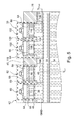
- FIG. 2 shows the block 6 of the integrated circuit 2 in greater detail.
- This circuit 2 comprises:
- the substrate 34 lies essentially in a plane called the “substrate plane”.
- the substrate plane is parallel to orthogonal horizontal directions X and Y and perpendicular to a vertical direction Z.
- This substrate plane forms a lower portion of the circuit 2 .
- this substrate 34 is p-doped with a doping concentration lower than or equal to 1 ⁇ 10 16 cm ⁇ 3 or 3 ⁇ 10 15 cm ⁇ 3 .
- the substrate 34 is represented by a dotted line.
- this substrate 34 is electrically connected to an electrical ground potential GND of the circuit 2 .
- the circuit 2 furthermore comprises a deep buried well 35 .
- This well 35 extends continuously and parallel to the substrate plane 34 .
- This well 35 is located immediately on the substrate 34 .
- This well 35 allows the appearance of leakage currents towards the substrate 34 to be limited.
- the doping type of the well 35 is especially chosen to form a reverse biased p-n junction with the substrate 34 .
- the well 35 is n-doped.
- the well 35 is represented by a dotted line.
- the rows have a substantially rectilinear shape and all extend, within the block 6 , in the X-direction. These rows have the same width, measured in the Y-direction. These rows are placed parallel to one another and are contiguous, pairwise, along one of their edges parallel to the X-direction.
- the rows 36 and 37 are described.
- the rows 36 and 37 are arranged, in block 6 , parallel to each other and contiguous to each other.
- the row 36 comprises:
- first 38 and second 40 semiconductor wells having opposite doping types
- At least one cell for biasing the wells 38 and 40 .
- the well 38 is p-doped.
- the well 40 is n-doped.
- the wells 38 and 40 have a doping concentration comprised between 10 16 and 10 18 cm ⁇ 3 .
- the wells 38 and 40 are placed next to one another in a given plane, called the “well plane”, parallel to the substrate plane. These wells 38 and 40 each lie in this well plane, parallel to the X-direction. Here, these wells 38 and 40 are located above the deep well 35 . Thus, the risk of leakage currents appearing between the well 38 and the substrate 34 is reduced.
- Standard cells are placed next to one another in the row 36 , so that the wells 38 and 40 are common to all the cells of the row 36 .
- these standard cells have a substantially rectangular shape, with the same height as the rows.
- These standard cells are separated from one another by trench isolations 45 .
- trench isolations 45 For the sake of simplicity, only two identical standard cells 42 and 43 , immediately adjacent to each other, are shown in FIG. 2 . On the edge where the cells 42 and 43 touch each other, the trench isolation 45 is common to these cells 42 , 43 .
- the row 36 comprises a plurality of cells for biasing the wells 38 and 40 . These cells are regularly spaced in each row. For the sake of simplicity, only a bias cell 44 is described in detail.
- the cell 44 comprises two connectors 46 , 48 , electrically connected to the wells 38 and 40 , respectively. These connectors 46 and 48 are each able to electrically bias the wells 38 and 40 when an electrical bias is applied to said connector by a voltage source. For this purpose, these connectors 46 and 48 make direct electrical contact with the wells 38 and 40 , respectively.
- These connectors 46 and 48 each comprise, for example, a trench extending as far as the wells 38 and 40 , respectively, and filled with an electrically conductive material such as a metal. Thus, the respective wells of each row may be biased with a given electrical potential.
- the rows of block 6 are placed in a flipped row configuration: the positions of the wells are permutated from one row to the other in the Y-direction, such that two contiguous wells, and respectively belonging to two contiguous rows, have the same doping.
- the row 37 is identical to the row 36 , except that the positions of the wells are permutated.
- the wells of this row 37 corresponding to the wells 38 and 40 bear the numerical references 39 and 41 , respectively.
- the circuit 2 comprises:
- the network 50 is able to apply separate electrical biases to the wells 38 and 40 . To do this, here this network is electrically connected to the connectors 46 and 48 . In this example, the network is configured so that all the wells 38 and 39 , 40 and 41 of the rows of the block 6 having a given doping type are biased with the same electrical potential.
- the source 52 is able to deliver electrical voltages to the network 50 .
- FIG. 3 shows, in greater detail, a cell 42 of the row 36 .
- each cell here comprises two transistors, the drain of one of these transistors being electrically connected directly to the source of the other transistor of the same cell. In the rest of the description, to simplify the figures, this electrical connection between the two transistors of a given cell has not been shown.
- the cell 42 comprises metal-oxide-semiconductor (MOS) field-effect transistors 60 , 62 . These transistors 60 and 62 are produced in FDSOI technology. The transistors 60 and 62 are placed plumb with the wells 38 and 40 , respectively.
- MOS metal-oxide-semiconductor
- the transistor 60 comprises:
- a semiconductor layer 64 called the active layer
- a buried layer 66 of electrically insulating material located under the layer 64 ;
- a gate multilayer 68 located on the layer 64 and especially comprising a gate 70 ;
- a semiconductor ground plane 72 located under the layer 66 .
- the layer 64 forms a channel between a source 74 and a drain 76 .
- this layer 64 is fully depleted and has a very low doping level, typically lower than or equal to 10 15 cm ⁇ 3 .
- This layer 64 is smaller than or equal to 50 nm in thickness.
- thickness and depth are defined relative to the Z-direction. Depth is defined relative to a horizontal reference plane passing, for example, through the layer 66 .
- the layer 66 electrically isolates the layer 64 from the ground plane 72 .
- This layer 66 extends substantially parallel to the substrate plane.
- the layer 66 is here an ultra-thin buried oxide layer (UTBOX) and is smaller than 40 nm in thickness, and preferably smaller than or equal to 25 nm in thickness.
- UTBOX ultra-thin buried oxide layer
- electrically insulating material is here understood to mean a material the electrical resistivity of which, at a temperature of 20° C., is higher than or equal to 10 5 ⁇ m or to 10 6 ⁇ m.
- this layer 66 is made of silicon oxide (SiO 2 ).
- the ground plane 72 allows the electrostatic properties of the transistor 60 to be controlled by applying an electrical potential to this ground plane 72 .
- the ground plane 72 is located directly and only on the well 38 , so that its electrical bias can be applied by way of the well 38 .
- the ground plane 72 extends horizontally and is arranged immediately above the well 38 , so as to be located plumb with the layer 64 .
- a ground plane of a transistor has the same doping type as the well above which this ground plane is placed.
- the ground plane 72 thus has the same doping type as the doping of the well 38 .
- the doping concentration of the ground plane 72 is here comprised between 10 18 cm ⁇ 3 and 10 20 cm ⁇ 3 .
- this ground plane 72 has a thickness comprised between 50 nm and 300 nm, and preferably between 70 nm and 200 nm.
- the ground plane 72 and the well 38 are here fabricated from one and the same semiconductor material, by separate ion implantation steps. Each of the ground plane 72 and the well 38 have a separate doping profile.
- the transistor 60 is an nMOS transistor.
- the source 74 and the drain 76 are formed above the layer 64 .
- this transistor has an intermediate threshold voltage, i.e. it is an RVT (regular V T ) transistor.
- the transistor 62 is similar to the transistor 60 , except that here:
- the transistor 62 is a pMOS transistor
- the ground plane 72 is replaced by a semiconductor ground plane 80 located only above, and plumb with, the well 40 , and having the same doping type as the doping of the well 40 .
- the cell 42 comprises, in addition to the trench isolation 45 , a trench isolation 82 , in order to electrically isolate the transistors 60 , 62 from each other.
- isolation of the transistors 60 and 62 is especially understood to mean that the ground planes 72 and 80 are electrically isolated from each other.
- the trench isolation 45 allows the transistors 60 , 62 to be electrically isolated from standard cells adjacent to the cell 42 .
- the trench isolation 45 encircles, in a horizontal plane, the cell 42 over its entire external perimeter.
- the trench isolation 82 allows the transistors 60 and 62 of a given cell 42 to be electrically isolated from each other. In this example, the trench isolation 82 is located between the transistors 60 and 62 .
- trench isolations 45 and 82 each extend, in the Z-direction, from an upper side of the layer 64 as far as a lower end located in the well plane and here having one and the same depth. This end is here located in the wells 38 and 40 , at a depth greater than the depth of the ground planes 72 and 80 .
- These trench isolations 45 and 82 are made of an electrically insulating material.
- these trench isolations 45 and 82 are made of silicon oxide.
- the cell 30 ( FIG. 2 ) is able to receive an input clock signal, and to transmit an output clock signal to a cell 42 of the block 6 .
- the input clock signal is the clock signal CLK.
- This cell 30 is surrounded by rows, so as to be contiguous with standard cells. Here, this cell 30 is located in the extension of two rows of the block 6 . This cell 30 is here contiguous with the cells 42 and 43 of the row 36 .
- FIG. 4 shows the cell 30 in greater detail.
- This cell 30 comprises:
- transistors 100 , 102 are transistors 100 , 102 ;
- a semiconductor strip 106 encircling, in a horizontal plane, the well 104 .
- the transistors 100 and 102 are placed plumb with the well 104 . These transistors 100 and 102 are able to be connected to form a device optimizing the distribution of the signal CLK by the tree 4 .
- this device is a buffer.
- These transistors 100 and 102 are, for example, identical to the transistors 60 and 62 , except that the ground planes 72 and 80 are replaced by ground planes 108 and 110 , respectively.
- these ground planes 108 and 110 have the same doping type, of the identical type to the doping of the well 104 .
- the well 104 extends horizontally. This well 104 is located immediately below the ground planes 108 and 110 and, here, immediately above the well 35 . This well 104 has the same doping type as the doping of the well 38 . Here, this doping is therefore p-type.
- the doping concentration of the well 104 is, for example, substantially equal to the doping concentration of the well 38 .
- This well 104 extends to the same depth as the wells 38 and 40 , to within 10% or 5%. Thus, this well 104 lies in the plane of the wells 38 to 41 .
- the strip 106 is interposed between the well 104 and the wells 38 and 40 of the cells 42 contiguous with the cell 30 .
- This strip 106 especially allows the well 104 to be separated and electrically isolated from the wells 38 and 39 of the immediately adjacent rows.
- this strip 106 has the opposite doping type to the doping of the well 104 , so as to form a reverse bias p-n junction with the wells 104 , 38 and 39 .
- This strip 106 has a width such that the smallest distance separating the wells 104 and 38 is larger than or equal to a threshold value L 1 , as illustrated in FIG. 2 by the arrows 112 and 114 .
- this distance is measured in a horizontal direction.
- the threshold value especially depends on constraints imposed by design rules specific to the technology node of the fabrication process of the circuit 2 . These rules especially require a threshold value be respected for the distance between two p-doped wells. In this example, for a 28 nm technology, the threshold value is greater than or equal to 1 ⁇ m or 500 nm or 100 nm.
- the strip 106 is an n-doped semiconductor layer with a doping concentration substantially equal to that of the well 104 .
- This strip 106 extends parallel to the plane of the substrate 34 and uninterruptedly encircles the well 104 .
- This strip 106 has the same depth as the well 104 .
- This strip 106 is here contiguous, especially, with the well 40 and is able to be brought to the same electrical potential as the well 40 .
- the strip 106 makes it possible to electrically isolate the well 104 , while ensuring the value L 1 required by the design rules is respected, without consuming too much of the surface space of the circuit 2 .
- the clock tree cell 30 which occupies a smaller footprint, may therefore be placed much closer to the cells 42 while remaining protected from electrical interference due to these cells 42 .
- the network 50 is furthermore configured to make it possible to apply, to the well 104 , an electrical bias that is different from the electrical bias applied to the wells 38 and/or 40 .
- the cell 30 comprises a connector 116 ( FIG. 2 ) allowing the well 104 to be electrically biased.
- This connector 116 is, for example, identical to the connectors 46 and 48 , and therefore is electrically connected directly to the well 104 .
- the ground planes 108 and 110 may thus be electrically biased by way of the well 104 , and independently of the bias applied to the wells 38 and 40 .
- This biasing of the ground planes 108 and 110 allows the electrostatic properties of the transistors 100 and 102 to be controlled. This control especially allows asymmetry between the electrical properties of the transistors 100 and 102 to be dynamically compensated.
- the transistors 100 and 102 of the cell 30 here form a CMOS (complementary metal-oxide-semiconductor) logic element.
- the transistors 100 and 102 here have a beta ratio chosen so that the rise time and fall time of the output clock signal transmitted by this cell 30 are substantially equal.
- Modification of this beta ratio may adversely affect the behaviour of the tree 4 .
- This asymmetry may depend on uncontrollable and/or unpredictable parameters, such as the operating environment of the circuit 2 (temperature for example), or random variations in the fabrication process of the circuit 2 .
- the cell 30 also comprises trench isolations 118 and 120 .
- the trench isolations 118 and 120 have similar functions to those of the trench isolations 45 and 82 , respectively, of the cell 42 .
- the trench isolation 120 is, for example, identical to the trench isolation 82 .
- the trench isolation 118 is produced in the same way as the trench isolation 45 , but may have a larger width in the Y-direction. In this example, the trench isolation 118 forms only a single block of material with the trench isolation 45 of the cells 42 , 43 that are immediately contiguous with this cell 30 , on the sites where the cell 30 is contiguous with these cells 42 , 43 .
- the cell 30 comprises passive electrical components such as an antenna diode 124 or a decoupling capacitor 126 ( FIG. 2 ), which components are located above the layer 66 and plumb with the strip 106 . These components may be electrically connected to other elements of the circuit 2 or of the cell 30 .
- passive electrical components such as an antenna diode 124 or a decoupling capacitor 126 ( FIG. 2 ), which components are located above the layer 66 and plumb with the strip 106 . These components may be electrically connected to other elements of the circuit 2 or of the cell 30 .
- Integrated circuits comprise such passive electrical components 124 , 126 .
- that portion of the cell 30 which is located plumb with the well 106 has a large footprint on which it is undesirable to place a transistor.
- this surface space is used for the elements 124 , 126 .
- the diode 124 protects the cell 30 from antenna effects possibly occurring during fabrication steps of the circuit 2 .
- the diode 124 is electrically connected between a portion of the interconnect network forming the tree 4 , and a reference electrical potential, in order to limit the risk of electrical charge accumulated in this portion of the interconnect network during manufacture of this network degrading the electrical properties of the cell 30 .
- This reference potential is, for example, the ground potential GND. In order to simplify FIG. 2 , this connection is not shown.
- This diode 124 is, for example, a p-n diode formed above the layer 66 .
- the capacitor 126 is electrically connected between either one of the transistors 100 and 102 and the reference electrical potential, in order to protect this transistor 100 or 102 from electrical disruption that could occur during operation of the circuit 2 .
- the capacitor 126 comprises a metal-insulator-metal (MIM) capacitor formed in the “metallization” levels of the circuit 2 during steps of producing the electrical interconnects (interconnect layers) of the circuit 2 .
- MIM metal-insulator-metal
- FIG. 5 illustrates a block 140 able to be used instead of the block 6 .
- This block is identical to the block 6 , except that the rows are arranged in what is called a regular configuration (i.e. not a flipped row configuration).
- the row 37 is replaced by a row 142 .
- This row 142 is, for example, identical to the row 37 , except that the positions of the wells 39 and 41 are permutated.
- the well 104 and the strip 106 are dimensioned such as to respect the distance constraint imposed by the design rules, as illustrated by the arrow 144 .
- the distance constraint is the same as that of the block 6 .
- the circuit 2 is, for example, started up and supplied with power by an electrical voltage source.
- biases V PW and V NW are applied to the wells 38 and 40 , respectively.
- biases V PW and V NW are applied by the network 50 .
- these biases V PW and V NW are equal to the ground potential GND and a supply voltage VDD of the circuit, respectively.
- a bias V PCLK is applied to the well 104 .
- This bias V PCLK is less than or equal to the smallest bias value V NW applied at the same time to the well 40 , so as to limit the risk of forward biasing the p-n junction formed by contact between the well 104 and the strip 106 (the strip 106 being at the same electrical potential as the well 40 ).
- the voltage V PCLK equals ground potential GND.
- the deep well 35 is omitted.
- the wells 38 , 39 , 40 , 41 and 104 and the strip 106 make direct contact with the substrate 34 .
- the biases V PW and V NW are adapted to prevent these wells 40 , 41 and this strip 106 from forming, with the substrate 34 , forward biased p-n junctions.
- the network 50 is configured so that the bias V PW equals ground potential GND.
- the cell 30 may provide functions other than a buffer function.
- the cell 30 is, for example, adapted to control the propagation of the input clock signal using another control signal (gated clock).
- the transistors 60 , 62 of the block 6 could have another threshold voltage.
- these transistors could be HVT or LVT transistors.
- the biases V PW and V NW may have different values from those described.
- the source 74 and the drain 76 are not formed on the layer 64 but are formed inside this layer 64 .
- the circuit 2 illustrated in FIG. 1 may be different from the example illustrated and may especially comprise more logic and/or synchronous elements.
- the assembly 20 may have more than one input IN and/or more than one output OUT.
- the cell 42 may comprise more than two transistors 60 and 62 .
- the connector 46 of the well 38 is omitted in the case where the wells 38 and 39 have the same doping type and are contiguous, and the well 39 already comprises a connector that is identical to the connector 46 .
- the connector 48 and the well 40 are also true.
- the capacitor 126 may be formed in the semiconductor layer located above the layer 66 , for example by means of a reverse biased p-n junction or a MOS transistor.
- the source 52 may be omitted.
- the network 50 is electrically connected to an electrical power source located outside of the circuit 2 .
- biases V NW and V PW may vary over time. These biases V NW and V PW may be modulated by a variable value ⁇ V, for example in order to apply a reverse back bias (RBB) or a forward back bias (FBB). The same is true for the bias V PCLK . These biases V NW , V PW and V PCLK may be applied in a different order from that described.
- the substrate 34 may be n-doped.
- the well 35 is n-doped.
- the elements 124 and 126 may be omitted.
- each pMOS transistor is located on an n-doped well and ground plane.
- each nMOS transistor is located on a p-doped well and ground plane.
- the transistors placed on the p-doped well 104 are both nMOS transistors.
- the one or more pMOS transistors of the clock tree cell are then placed in the n-doped strip 106 .
- the strip 106 is modified to extend not only around the well 104 but also around the ground plane of the nMOS transistors.
Landscapes
- Engineering & Computer Science (AREA)
- Physics & Mathematics (AREA)
- General Physics & Mathematics (AREA)
- Theoretical Computer Science (AREA)
- Electromagnetism (AREA)
- Radar, Positioning & Navigation (AREA)
- Automation & Control Theory (AREA)
- General Engineering & Computer Science (AREA)
- Semiconductor Integrated Circuits (AREA)
- Metal-Oxide And Bipolar Metal-Oxide Semiconductor Integrated Circuits (AREA)
- Design And Manufacture Of Integrated Circuits (AREA)
Abstract
-
- a block comprising:
- first (38) and second (40) oppositely doped semiconductor wells;
- standard cells (42, 43) placed next to one another, each standard cell (42) comprising first transistors (60, 62), and a clock tree cell (30) encircled by standard cells, the clock tree cell (30) comprising:
- a third semiconductor well (104) having the same doping type as the doping of the first well (38);
- second transistors (100, 102);
- a semiconductor strip (106) extending continuously around the third well (104), and having the opposite doping type to the doping of the third well, so as to electrically isolate the third well (104) from the first well (38).
- a block comprising:
Description
- Under 35 USC 119, this application claims the benefit of the priority date of French Patent Application 1262812, filed Dec. 26, 2012, the content of which is herein incorporated by reference.
- The invention relates to an integrated circuit. The invention also relates to a method of using this integrated circuit.
- The invention is in particular applicable to integrated circuits produced on a silicon-on-insulator (SOI) substrate. SOI technology consists in separating a thin silicon layer (a few nanometres in thickness) from a silicon substrate, using a relatively thick insulating layer (a few tens of nanometres in thickness as a general rule).
- Integrated circuits produced by SOI technology exhibit a certain number of advantages. Such circuits generally have a lower power consumption for an equivalent performance, or a better performance for a given consumption. Such circuits also induce lower parasitic capacitances, which make it possible to improve switching speed. In addition, latch up, which is encountered in bulk technology metal-oxide-semiconductor (MOS) transistors, may be prevented. Such circuits therefore prove to be particularly suitable for system on chip (SoC) or microelectromechanical system (MEMS) applications. It is also noted that SOI integrated circuits are less sensitive to the effects of ionizing radiations and thus turn out to be more reliable in applications where such radiations may induce operational problems, in particular in space applications. SOI integrated circuits may notably comprise active static random access memory (SRAM) or logic gates.
- The reduction in the static consumption of logic gates while increasing their toggling speed forms the subject of much research. Certain integrated circuits currently being developed integrate at one and the same time logic gates with low consumption and logic gates with high toggling speed. To generate these two types of logic gates in a given integrated circuit, the threshold voltage (abbreviated VT) of certain transistors is decreased to form fast-access logic gates, and the threshold voltage of other transistors is increased to form low-consumption logic gates. In bulk technology, modulation of the threshold voltage level of transistors of the same type is mainly achieved by modifying their channel doping level. However, in FDSOI (fully depleted silicon-on-insulator) technology channel doping is almost inexistent
- (1015 cm−3). Thus, the doping level of the channel of the transistors therefore cannot exhibit any significant variations, thus preventing the threshold voltages from being differentiated in this way. One solution proposed in certain studies, in order to produce transistors of the same type with different threshold voltages, is to use different gate materials in these transistors. However, the practical production of an integrated circuit such as this turns out to be technically tricky and economically prohibitive.
- In order for different transistors produced in FDSOI technology to have different threshold voltages it is also known to use an electrically biased ground plane (or back plane) placed between a thin insulating oxide layer and the silicon substrate. By adjusting the doping type of the ground planes and their electrical bias, it is possible to improve electrostatic control of these transistors, thereby allowing different threshold-voltage ranges to be defined for these transistors. It is thus possible to produce transistors with a low threshold voltage, termed LVT (for low VT) transistors, transistors with a high threshold voltage, termed HVT (for high VT) transistors, and transistors with an intermediate threshold voltage, termed SVT (for standard VT) or RVT (for regular VT) transistors. Typically, the threshold voltage of LVT transistors is 350 mV or less, that of HVT transistors 500 mV or more, and that of RVT transistors comprised between 350 mV and 500 mV.
- Such transistors are for example described in the technical application note by P. Flatresse et al., “Planar fully depleted silicon technology to design competitive SOC at 28 nm and beyond”, STMicroelectronics, 2012, available on the website “www.soiconsortium.org”.
- The state-of-the-art is also described in the following documents:
- WO 2012/160071 A1 (CEA);
- Jean-Philippe Noel et al. “Multi-VT UTBB FDSOI device architectures for low-power CMOS circuit”; IEEE Transactions on Electron Devices, vol. 58, p. 2473-2482, August 2011; and
- US 2006/027877 A1 (INABA).
- As is known, synchronous logic integrated circuits require a clock signal to synchronize operation of the logic elements of the circuit. Typically, this clock signal is distributed from a clock signal generator to elements of the circuit, such as registers or switches, by way of a clock tree. This clock tree is a network of electrical interconnects that typically has a tree-like structure, comprising a common trunk, connected to the clock signal generator, dividing into a multitude of branches. Each of these branches may itself divide into a plurality of additional branches.
- To ensure correct operation of the circuit, and especially to prevent setup and hold time violations, this clock tree must be carefully configured to limit the appearance of differences in the propagation time of the clock signal (clock skew). For this purpose, the clock tree typically comprises clock tree cells that implement functions optimizing the distribution of the clock signal, such as buffer functions. Thus, each clock tree cell is connected to a branch of the clock tree, and receives an input clock signal from this clock tree. This clock tree cell is also adapted to deliver an output clock signal, able to be distributed to the logic elements of the circuit. In the case where the clock tree cell acts as a buffer, the output clock signal is identical to the input clock signal except that it is delayed by a preset amount of time. These buffers may be adapted, during design of the integrated circuit, to balance the branches of the clock tree and control the appearance of clock skew.
- However, integrating such clock tree cells into a circuit comprising standard cells in FDSOI technology with different threshold voltages causes a number of problems.
- Typically, the circuit also comprises standard cells, containing transistors connected to form the logic elements of the circuit. In this description, the term “standard cell” is understood to mean an integrated-circuit portion corresponding to the physical implementation of a cell of a library of an integrated-circuit design program. Therefore, the standard cells are not necessarily all identical to one another. In contrast, these standard cells do not belong to the clock tree.
- In 28 nm FDSOI technology, these standard cells are typically arranged in the circuit in the form of blocks. Standard cells belonging to a given block all have the same threshold-voltage range. When a number of blocks are implanted on a given substrate, each block comprises its own deep buried well, above which each of the standard cells of this block are produced in order to isolate them electrically from the substrate. If such a deep buried well does not exist, all the standard cells produced on the substrate are considered to belong to the same block. Each block has a regular shape and contains a number of contiguous standard cells. Here, cells are said to be “contiguous” if they are separated from one another only by a trench isolation, typically a deep trench isolation. Here, each block has a substantially rectangular shape. Two separate blocks, and in particular their respective deep buried wells, are spaced apart from each other by a strip-shaped separating zone. This strip is, for example, larger than or equal to a few microns in width. Preferably, no transistors are implanted in this separating zone.
- Clock tree cells located at the ends of the branches are electrically connected to the standard cells in order to transmit the output clock signal to them. These clock tree cells located at the ends of the branches are called leaves of the clock tree.
- Commonly used clock tree cells are structurally similar to the standard cells of the circuit. Leaf cells of the clock tree are preferably integrated into each block as near as possible to the standard cells, especially in order to reduce the length of the electrical connections connecting these leaf cells to the neighbouring standard cells.
- It would therefore be desirable to provide an integrated circuit comprising transistors in 28 nm FDSOI technology, this circuit comprising a clock tree cell that is able to be electrically controlled independently from the standard cells of the circuit, while minimizing the footprint required to integrate this clock tree cell into a block of standard cells, i.e. cells comprising transistors with a given threshold voltage.
- However, in each block of the circuit, the clock tree cell must be sufficiently isolated from adjacent standard cells to prevent its operation from being affected by the electrical biases applied to the ground plane of the standard cells. With current 28 nm FDSOI technology design rules, such a clock tree cell is separated from standard cells by a spacing of several microns, thereby wasting as much as 10% of the footprint of the block. Such wasted space limits the number of logic elements that can be produced in the circuit, which is not economically acceptable.
- Thus, the invention relates to an integrated circuit according to Claim 1.
- Thus, the clock tree cell may be integrated into a block of standard cells, while keeping a small footprint as it comprises only a single semiconductor well. This well of the clock tree cell is electrically isolated from those wells of adjacent standard cells which have the same doping type, by surrounding it with an oppositely doped semiconductor strip. This strip makes contact with this well of the clock tree cell so as to form a reverse biased p-n junction, thereby ensuring electrical isolation of these cells from one another. This specific configuration makes it possible to circumvent design rules that required a large spacing between these cells, and thus allows the footprint occupied by the clock tree cell to be decreased.
- Embodiments of the invention may comprise one or more of the features of
Claims 2 to 12. - These embodiments furthermore have the following advantages:
- the deep buried well allows the substrate to be electrically isolated from the first and third wells, thereby limiting the risk of a leakage current appearing between these wells and the substrate; and
- that portion of the clock tree cell which is located above the semiconductor strip may be used to locate antenna diodes or decoupling capacitors that, otherwise, would have to be located in other positions in the circuit, thereby allowing the footprint occupied by the block of standard cells to be decreased.
- The invention also relates to a method for using an integrated circuit according to Claim 13.
- The invention will be better understood on reading the following description, given merely by way of non-limiting example and with reference to the drawings in which:
-
FIG. 1 is a schematic illustration of a portion of an integrated circuit comprising a clock tree; -
FIG. 2 is a schematic illustration of a longitudinal cross section through a block of the integrated circuit inFIG. 1 ; -
FIG. 3 is a schematic cross-sectional view of a row of the block inFIG. 2 ; -
FIG. 4 is a schematic cross-sectional view of a clock tree cell of the block inFIG. 2 ; -
FIG. 5 is a schematic cross-sectional view of the cells inFIGS. 3 and 4 , placed side-by-side; -
FIG. 6 is a schematic illustration of another embodiment of the block inFIG. 2 ; and -
FIG. 7 is a flowchart of a method for using the integrated circuit inFIG. 1 . - In these figures, the same references are used to denote the same elements.
- In the rest of the description, features and functions that are well known in the art will not be described in detail.
-
FIG. 1 shows, in a simplified way, a portion of anintegrated circuit 2 containing aclock tree 4. In this example, thecircuit 2 comprisesblocks blocks block block 6 have a separate threshold-voltage range from that of the transistors of theblock 8. In this case, the respective transistors of theseblocks logic elements synchronous elements elements assembly 20 configured to perform a preset logic function. Thisassembly 20 is configured to receive an input signal IN transmitted from theblock 6, and to deliver an output signal OUT in response to the signal IN, generated in theblock 8. Theclock tree 4 is able to transmit a clock signal CLK to theelements circuit 2, such that this signal CLK is received simultaneously by theseelements assembly 20 with that of the rest of thecircuit 2. In this example, the signal CLK transmitted by theelement 16 is a periodic square wave signal. - This
clock tree 4 is a network of electrical interconnects here taking a tree-like form comprising a plurality of branches. For the sake of simplicity, only twobranches tree 4 are shown. In this example, thebranch 22 is connected to a clock input of theelement 16, and thebranch 24 is connected to a clock input of theelement 18. In order to limit differences in the propagation time of the signal CLK in thebranches tree 4 comprises a plurality of clock tree cells. Each of these clock cells is here configured to delay the propagation of the signal CLK by a preset delay time. Thus, selectively adding clock tree cells in the branches of thetree 4 allows these differences in propagation time to be decreased. In this example, only twoclock tree cells cells tree 4. Thesecells blocks cells cell 30 is located inside theblock 6 and thecell 32 is located inside theblock 8. - In this description, two similar cells may have geometric differences, for example made necessary by the circuit design steps, in order to adapt these cells for electrical connection with other cells of the circuit, contiguous with these cells.
-
FIG. 2 shows theblock 6 of theintegrated circuit 2 in greater detail. Thiscircuit 2 comprises: - a
semiconductor substrate 34; - a plurality of rows of standard cells; and
- the
clock tree cell 30. - The
substrate 34 lies essentially in a plane called the “substrate plane”. Here, the substrate plane is parallel to orthogonal horizontal directions X and Y and perpendicular to a vertical direction Z. This substrate plane forms a lower portion of thecircuit 2. Here thissubstrate 34 is p-doped with a doping concentration lower than or equal to 1×1016 cm−3 or 3×1015 cm−3. To simplifyFIG. 2 thesubstrate 34 is represented by a dotted line. Here, thissubstrate 34 is electrically connected to an electrical ground potential GND of thecircuit 2. - Advantageously, the
circuit 2 furthermore comprises a deep buried well 35. This well 35 extends continuously and parallel to thesubstrate plane 34. This well 35 is located immediately on thesubstrate 34. This well 35 allows the appearance of leakage currents towards thesubstrate 34 to be limited. For this purpose, the doping type of the well 35 is especially chosen to form a reverse biased p-n junction with thesubstrate 34. Here, the well 35 is n-doped. In order to simplifyFIG. 2 , the well 35 is represented by a dotted line. - Here the rows have a substantially rectilinear shape and all extend, within the
block 6, in the X-direction. These rows have the same width, measured in the Y-direction. These rows are placed parallel to one another and are contiguous, pairwise, along one of their edges parallel to the X-direction. - For the sake of simplicity only the
rows rows block 6, parallel to each other and contiguous to each other. - The
row 36 comprises: - first 38 and second 40 semiconductor wells, having opposite doping types;
- a plurality of standard cells; and
- at least one cell for biasing the
wells - In this example, the well 38 is p-doped. The well 40 is n-doped. The
wells - The
wells wells wells deep well 35. Thus, the risk of leakage currents appearing between the well 38 and thesubstrate 34 is reduced. - Standard cells are placed next to one another in the
row 36, so that thewells row 36. Here, these standard cells have a substantially rectangular shape, with the same height as the rows. These standard cells are separated from one another bytrench isolations 45. For the sake of simplicity, only twoidentical standard cells FIG. 2 . On the edge where thecells trench isolation 45 is common to thesecells - Here, the
row 36 comprises a plurality of cells for biasing thewells bias cell 44 is described in detail. Thecell 44 comprises twoconnectors wells connectors wells connectors wells connectors wells - In this description, two elements are said to make direct contact if they are in immediate physical contact with each other and if no other element of different nature is interposed between these two elements.
- In this example, the rows of
block 6 are placed in a flipped row configuration: the positions of the wells are permutated from one row to the other in the Y-direction, such that two contiguous wells, and respectively belonging to two contiguous rows, have the same doping. Here, therow 37 is identical to therow 36, except that the positions of the wells are permutated. InFIG. 2 , the wells of thisrow 37 corresponding to thewells numerical references - Advantageously, the
circuit 2 comprises: - an electrical
power supply network 50; and - an
electrical power source 52. - The
network 50 is able to apply separate electrical biases to thewells connectors wells block 6 having a given doping type are biased with the same electrical potential. - The
source 52 is able to deliver electrical voltages to thenetwork 50. -
FIG. 3 shows, in greater detail, acell 42 of therow 36. Typically, each cell here comprises two transistors, the drain of one of these transistors being electrically connected directly to the source of the other transistor of the same cell. In the rest of the description, to simplify the figures, this electrical connection between the two transistors of a given cell has not been shown. Thecell 42 comprises metal-oxide-semiconductor (MOS) field-effect transistors transistors transistors wells - Thus, the
transistor 60 comprises: - a
semiconductor layer 64, called the active layer; - a buried
layer 66 of electrically insulating material, located under thelayer 64; - a
gate multilayer 68, located on thelayer 64 and especially comprising agate 70; and - a
semiconductor ground plane 72, located under thelayer 66. - The
layer 64 forms a channel between asource 74 and adrain 76. As is known, in FDSOI technology thislayer 64 is fully depleted and has a very low doping level, typically lower than or equal to 1015 cm−3. Thislayer 64 is smaller than or equal to 50 nm in thickness. - In this description, thickness and depth are defined relative to the Z-direction. Depth is defined relative to a horizontal reference plane passing, for example, through the
layer 66. - The
layer 66 electrically isolates thelayer 64 from theground plane 72. Thislayer 66 extends substantially parallel to the substrate plane. Thelayer 66 is here an ultra-thin buried oxide layer (UTBOX) and is smaller than 40 nm in thickness, and preferably smaller than or equal to 25 nm in thickness. The expression “electrically insulating material” is here understood to mean a material the electrical resistivity of which, at a temperature of 20° C., is higher than or equal to 105 Ω·m or to 106 Ω·m. For example, here thislayer 66 is made of silicon oxide (SiO2). - The
ground plane 72 allows the electrostatic properties of thetransistor 60 to be controlled by applying an electrical potential to thisground plane 72. Theground plane 72 is located directly and only on the well 38, so that its electrical bias can be applied by way of the well 38. For this purpose, theground plane 72 extends horizontally and is arranged immediately above the well 38, so as to be located plumb with thelayer 64. - In this example, a ground plane of a transistor has the same doping type as the well above which this ground plane is placed. Here, the
ground plane 72 thus has the same doping type as the doping of the well 38. The doping concentration of theground plane 72 is here comprised between 1018 cm−3 and 1020 cm−3. Here, thisground plane 72 has a thickness comprised between 50 nm and 300 nm, and preferably between 70 nm and 200 nm. Theground plane 72 and the well 38 are here fabricated from one and the same semiconductor material, by separate ion implantation steps. Each of theground plane 72 and the well 38 have a separate doping profile. - In this example, the
transistor 60 is an nMOS transistor. Here, thesource 74 and thedrain 76 are formed above thelayer 64. Here, this transistor has an intermediate threshold voltage, i.e. it is an RVT (regular VT) transistor. - The
transistor 62 is similar to thetransistor 60, except that here: - the
transistor 62 is a pMOS transistor; and - the
ground plane 72 is replaced by asemiconductor ground plane 80 located only above, and plumb with, the well 40, and having the same doping type as the doping of the well 40. - For example, apart from the above differences, everything that was described with reference to the
transistor 60 applies to thetransistor 62. - The
cell 42 comprises, in addition to thetrench isolation 45, atrench isolation 82, in order to electrically isolate thetransistors transistors trench isolation 45 allows thetransistors cell 42. For this purpose, thetrench isolation 45 encircles, in a horizontal plane, thecell 42 over its entire external perimeter. Thetrench isolation 82 allows thetransistors cell 42 to be electrically isolated from each other. In this example, thetrench isolation 82 is located between thetransistors trench isolations layer 64 as far as a lower end located in the well plane and here having one and the same depth. This end is here located in thewells trench isolations trench isolations - The cell 30 (
FIG. 2 ) is able to receive an input clock signal, and to transmit an output clock signal to acell 42 of theblock 6. Here, the input clock signal is the clock signal CLK. Thiscell 30 is surrounded by rows, so as to be contiguous with standard cells. Here, thiscell 30 is located in the extension of two rows of theblock 6. Thiscell 30 is here contiguous with thecells row 36. -
FIG. 4 shows thecell 30 in greater detail. Thiscell 30 comprises: -
transistors - a single semiconductor well 104 common to all the transistors of the
cell 30; and - a
semiconductor strip 106 encircling, in a horizontal plane, thewell 104. - The
transistors well 104. Thesetransistors tree 4. Here, this device is a buffer. Thesetransistors transistors ground planes ground planes well 104. - The well 104 extends horizontally. This well 104 is located immediately below the ground planes 108 and 110 and, here, immediately above the
well 35. This well 104 has the same doping type as the doping of the well 38. Here, this doping is therefore p-type. The doping concentration of the well 104 is, for example, substantially equal to the doping concentration of the well 38. This well 104 extends to the same depth as thewells wells 38 to 41. - The
strip 106 is interposed between the well 104 and thewells cells 42 contiguous with thecell 30. Thisstrip 106 especially allows the well 104 to be separated and electrically isolated from thewells strip 106 has the opposite doping type to the doping of the well 104, so as to form a reverse bias p-n junction with thewells - This
strip 106 has a width such that the smallest distance separating thewells FIG. 2 by thearrows 112 and 114. Here, this distance is measured in a horizontal direction. The threshold value especially depends on constraints imposed by design rules specific to the technology node of the fabrication process of thecircuit 2. These rules especially require a threshold value be respected for the distance between two p-doped wells. In this example, for a 28 nm technology, the threshold value is greater than or equal to 1 μm or 500 nm or 100 nm. - Here, the
strip 106 is an n-doped semiconductor layer with a doping concentration substantially equal to that of thewell 104. Thisstrip 106 extends parallel to the plane of thesubstrate 34 and uninterruptedly encircles thewell 104. Thisstrip 106 has the same depth as thewell 104. Thisstrip 106 is here contiguous, especially, with the well 40 and is able to be brought to the same electrical potential as thewell 40. - Thus, the
strip 106 makes it possible to electrically isolate the well 104, while ensuring the value L1 required by the design rules is respected, without consuming too much of the surface space of thecircuit 2. Theclock tree cell 30, which occupies a smaller footprint, may therefore be placed much closer to thecells 42 while remaining protected from electrical interference due to thesecells 42. - In this example, the
network 50 is furthermore configured to make it possible to apply, to the well 104, an electrical bias that is different from the electrical bias applied to thewells 38 and/or 40. - Advantageously, the
cell 30 comprises a connector 116 (FIG. 2 ) allowing the well 104 to be electrically biased. Thisconnector 116 is, for example, identical to theconnectors well 104. - The ground planes 108 and 110 may thus be electrically biased by way of the well 104, and independently of the bias applied to the
wells transistors transistors - Specifically, the
transistors cell 30 here form a CMOS (complementary metal-oxide-semiconductor) logic element. Thetransistors cell 30 are substantially equal. - Modification of this beta ratio, creating what is called an asymmetry between the transistors of a given clock tree cell, may adversely affect the behaviour of the
tree 4. This asymmetry may depend on uncontrollable and/or unpredictable parameters, such as the operating environment of the circuit 2 (temperature for example), or random variations in the fabrication process of thecircuit 2. - Here, the
cell 30 also comprisestrench isolations trench isolations cell 42. Thetrench isolation 120 is, for example, identical to thetrench isolation 82. Thetrench isolation 118 is produced in the same way as thetrench isolation 45, but may have a larger width in the Y-direction. In this example, thetrench isolation 118 forms only a single block of material with thetrench isolation 45 of thecells cell 30, on the sites where thecell 30 is contiguous with thesecells - Advantageously, the
cell 30 comprises passive electrical components such as anantenna diode 124 or a decoupling capacitor 126 (FIG. 2 ), which components are located above thelayer 66 and plumb with thestrip 106. These components may be electrically connected to other elements of thecircuit 2 or of thecell 30. - Integrated circuits comprise such passive
electrical components cell 30 which is located plumb with the well 106 has a large footprint on which it is undesirable to place a transistor. Thus, this surface space is used for theelements elements circuit 2. - In this example, the
diode 124 protects thecell 30 from antenna effects possibly occurring during fabrication steps of thecircuit 2. For this purpose, thediode 124 is electrically connected between a portion of the interconnect network forming thetree 4, and a reference electrical potential, in order to limit the risk of electrical charge accumulated in this portion of the interconnect network during manufacture of this network degrading the electrical properties of thecell 30. This reference potential is, for example, the ground potential GND. In order to simplifyFIG. 2 , this connection is not shown. Thisdiode 124 is, for example, a p-n diode formed above thelayer 66. - Here, the
capacitor 126 is electrically connected between either one of thetransistors transistor circuit 2. - For example, the
capacitor 126 comprises a metal-insulator-metal (MIM) capacitor formed in the “metallization” levels of thecircuit 2 during steps of producing the electrical interconnects (interconnect layers) of thecircuit 2. -
FIG. 5 illustrates ablock 140 able to be used instead of theblock 6. This block is identical to theblock 6, except that the rows are arranged in what is called a regular configuration (i.e. not a flipped row configuration). For this purpose, therow 37 is replaced by arow 142. Thisrow 142 is, for example, identical to therow 37, except that the positions of thewells - With this arrangement of the wells, the well 104 and the
strip 106 are dimensioned such as to respect the distance constraint imposed by the design rules, as illustrated by the arrow 144. For example, the distance constraint is the same as that of theblock 6. - An example of the operation of the
integrated circuit 2 will now be described with reference to the method inFIG. 7 and with the aid ofFIGS. 2 and 3 . - In a
step 200, thecircuit 2 is, for example, started up and supplied with power by an electrical voltage source. - In a
step 202, biases VPW and VNW are applied to thewells - Here, these biases VPW and VNW are applied by the
network 50. Here, these biases VPW and VNW are equal to the ground potential GND and a supply voltage VDD of the circuit, respectively. - In a
step 204, a bias VPCLK is applied to thewell 104. This bias VPCLK is less than or equal to the smallest bias value VNW applied at the same time to the well 40, so as to limit the risk of forward biasing the p-n junction formed by contact between the well 104 and the strip 106 (thestrip 106 being at the same electrical potential as the well 40). Here, the voltage VPCLK equals ground potential GND. - Many other embodiments are possible.
- As a variant, the
deep well 35 is omitted. In this case, thewells strip 106 make direct contact with thesubstrate 34. In order to limit the appearance of leakage currents between thewells strip 106, on the other hand, via thesubstrate 34, the biases VPW and VNW are adapted to prevent thesewells strip 106 from forming, with thesubstrate 34, forward biased p-n junctions. To do this, thenetwork 50 is configured so that the bias VPW equals ground potential GND. - The
cell 30 may provide functions other than a buffer function. Thecell 30 is, for example, adapted to control the propagation of the input clock signal using another control signal (gated clock). - The
transistors block 6 could have another threshold voltage. For example these transistors could be HVT or LVT transistors. In this case, the biases VPW and VNW may have different values from those described. - As a variant, the
source 74 and thedrain 76 are not formed on thelayer 64 but are formed inside thislayer 64. - The
circuit 2 illustrated inFIG. 1 may be different from the example illustrated and may especially comprise more logic and/or synchronous elements. Theassembly 20 may have more than one input IN and/or more than one output OUT. - The
cell 42 may comprise more than twotransistors - As a variant, the
connector 46 of the well 38 is omitted in the case where thewells connector 46. The same is also true for theconnector 48 and the well 40. - The
capacitor 126 may be formed in the semiconductor layer located above thelayer 66, for example by means of a reverse biased p-n junction or a MOS transistor. - The
source 52 may be omitted. In this case, thenetwork 50 is electrically connected to an electrical power source located outside of thecircuit 2. - The biases VNW and VPW may vary over time. These biases VNW and VPW may be modulated by a variable value ΔV, for example in order to apply a reverse back bias (RBB) or a forward back bias (FBB). The same is true for the bias VPCLK. These biases VNW, VPW and VPCLK may be applied in a different order from that described.
- The
substrate 34 may be n-doped. In this case the well 35 is n-doped. - The
elements - The above description also applies to the case where the cells comprise non-FDSOI transistors and, in particular, transistors without the buried
layer 66. Such transistors without a buried insulating layer between thelayer 64 and the ground plane are said to be produced in “bulk” technology. In this case, each pMOS transistor is located on an n-doped well and ground plane. In contrast, each nMOS transistor is located on a p-doped well and ground plane. Thus, in the case of bulk technology, the transistors placed on the p-doped well 104 are both nMOS transistors. If necessary, the one or more pMOS transistors of the clock tree cell are then placed in the n-dopedstrip 106. To do this, for example, thestrip 106 is modified to extend not only around the well 104 but also around the ground plane of the nMOS transistors.
Claims (13)
Applications Claiming Priority (2)
| Application Number | Priority Date | Filing Date | Title |
|---|---|---|---|
| FR1262812 | 2012-12-26 | ||
| FR1262812A FR3000296B1 (en) | 2012-12-26 | 2012-12-26 | INTEGRATED CIRCUIT COMPRISING A CLOCK TREE CELL |
Publications (2)
| Publication Number | Publication Date |
|---|---|
| US20140176216A1 true US20140176216A1 (en) | 2014-06-26 |
| US9000840B2 US9000840B2 (en) | 2015-04-07 |
Family
ID=48901011
Family Applications (1)
| Application Number | Title | Priority Date | Filing Date |
|---|---|---|---|
| US14/134,167 Active US9000840B2 (en) | 2012-12-26 | 2013-12-19 | Integrated circuit comprising a clock tree cell |
Country Status (3)
| Country | Link |
|---|---|
| US (1) | US9000840B2 (en) |
| EP (1) | EP2750180B1 (en) |
| FR (1) | FR3000296B1 (en) |
Cited By (9)
| Publication number | Priority date | Publication date | Assignee | Title |
|---|---|---|---|---|
| US20170125403A1 (en) * | 2015-10-28 | 2017-05-04 | Globalfoundries Inc. | Antenna diode circuit for manufacturing of semiconductor devices |
| CN107026176A (en) * | 2015-09-21 | 2017-08-08 | 格罗方德半导体公司 | Contact SOI substrate |
| US20170250197A1 (en) * | 2014-11-14 | 2017-08-31 | Socionext Inc. | Layout structure for semiconductor integrated circuit |
| DE102016215276B4 (en) | 2015-09-21 | 2019-12-19 | Globalfoundries Inc. | CONTACT SOI SUBSTRATES |
| CN112951844A (en) * | 2021-01-20 | 2021-06-11 | 广东省大湾区集成电路与系统应用研究院 | Standard unit library of FDSOI device |
| US20210234848A1 (en) * | 2018-01-11 | 2021-07-29 | Visa International Service Association | Offline authorization of interactions and controlled tasks |
| CN114141768A (en) * | 2020-09-04 | 2022-03-04 | 长鑫存储技术有限公司 | Semiconductor structure and manufacturing method thereof |
| CN115831875A (en) * | 2021-09-17 | 2023-03-21 | 意法半导体(鲁塞)公司 | Integrated circuit comprising standard cells and at least one capacitive fill structure |
| US20230195987A1 (en) * | 2020-08-04 | 2023-06-22 | Shenzhen Microbt Electronics Technology Co., Ltd. | Standard unit for system on chip design, and data processing unit, operation chip and computing apparatus using same |
Families Citing this family (2)
| Publication number | Priority date | Publication date | Assignee | Title |
|---|---|---|---|---|
| US9455250B1 (en) | 2015-06-30 | 2016-09-27 | International Business Machines Corporation | Distributed decoupling capacitor |
| US10002800B2 (en) | 2016-05-13 | 2018-06-19 | International Business Machines Corporation | Prevention of charging damage in full-depletion devices |
Citations (1)
| Publication number | Priority date | Publication date | Assignee | Title |
|---|---|---|---|---|
| US8631377B2 (en) * | 2009-05-14 | 2014-01-14 | Taiwan Semiconductor Manufacturing Company, Ltd. | System and method for designing cell rows with differing cell heights |
Family Cites Families (2)
| Publication number | Priority date | Publication date | Assignee | Title |
|---|---|---|---|---|
| JP4664631B2 (en) * | 2004-08-05 | 2011-04-06 | 株式会社東芝 | Semiconductor device and manufacturing method thereof |
| FR2975803B1 (en) * | 2011-05-24 | 2014-01-10 | Commissariat Energie Atomique | INTEGRATED CIRCUIT IN SELF COMPRISING ADJACENT CELLS OF DIFFERENT TYPES |
-
2012
- 2012-12-26 FR FR1262812A patent/FR3000296B1/en not_active Expired - Fee Related
-
2013
- 2013-12-18 EP EP13198071.6A patent/EP2750180B1/en active Active
- 2013-12-19 US US14/134,167 patent/US9000840B2/en active Active
Patent Citations (1)
| Publication number | Priority date | Publication date | Assignee | Title |
|---|---|---|---|---|
| US8631377B2 (en) * | 2009-05-14 | 2014-01-14 | Taiwan Semiconductor Manufacturing Company, Ltd. | System and method for designing cell rows with differing cell heights |
Cited By (16)
| Publication number | Priority date | Publication date | Assignee | Title |
|---|---|---|---|---|
| US20170250197A1 (en) * | 2014-11-14 | 2017-08-31 | Socionext Inc. | Layout structure for semiconductor integrated circuit |
| CN107026176A (en) * | 2015-09-21 | 2017-08-08 | 格罗方德半导体公司 | Contact SOI substrate |
| DE102016215276B4 (en) | 2015-09-21 | 2019-12-19 | Globalfoundries Inc. | CONTACT SOI SUBSTRATES |
| US20170125403A1 (en) * | 2015-10-28 | 2017-05-04 | Globalfoundries Inc. | Antenna diode circuit for manufacturing of semiconductor devices |
| CN107039416A (en) * | 2015-10-28 | 2017-08-11 | 格罗方德半导体公司 | Manufacture the antenna diodes circuit of semiconductor device |
| US10096595B2 (en) * | 2015-10-28 | 2018-10-09 | Globalfoundries Inc. | Antenna diode circuit for manufacturing of semiconductor devices |
| TWI645536B (en) * | 2015-10-28 | 2018-12-21 | Globalfoundries Us Inc. | Antenna diode circuit for manufacturing a semiconductor device |
| US20210234848A1 (en) * | 2018-01-11 | 2021-07-29 | Visa International Service Association | Offline authorization of interactions and controlled tasks |
| US11855971B2 (en) * | 2018-01-11 | 2023-12-26 | Visa International Service Association | Offline authorization of interactions and controlled tasks |
| US20230195987A1 (en) * | 2020-08-04 | 2023-06-22 | Shenzhen Microbt Electronics Technology Co., Ltd. | Standard unit for system on chip design, and data processing unit, operation chip and computing apparatus using same |
| US11768988B2 (en) * | 2020-08-04 | 2023-09-26 | Shenzhen Microbt Electronics Technology Co., Ltd. | Standard unit for system on chip design, and data processing unit, operation chip and computing apparatus using same |
| CN114141768A (en) * | 2020-09-04 | 2022-03-04 | 长鑫存储技术有限公司 | Semiconductor structure and manufacturing method thereof |
| WO2022048216A1 (en) * | 2020-09-04 | 2022-03-10 | 长鑫存储技术有限公司 | Semiconductor structure and manufacturing method therefor |
| US12211852B2 (en) * | 2020-09-04 | 2025-01-28 | Changxin Memory Technologies, Inc. | Semiconductor structure with a second isolation dam and manufacturing method thereof |
| CN112951844A (en) * | 2021-01-20 | 2021-06-11 | 广东省大湾区集成电路与系统应用研究院 | Standard unit library of FDSOI device |
| CN115831875A (en) * | 2021-09-17 | 2023-03-21 | 意法半导体(鲁塞)公司 | Integrated circuit comprising standard cells and at least one capacitive fill structure |
Also Published As
| Publication number | Publication date |
|---|---|
| FR3000296A1 (en) | 2014-06-27 |
| US9000840B2 (en) | 2015-04-07 |
| EP2750180A3 (en) | 2017-11-29 |
| EP2750180A2 (en) | 2014-07-02 |
| EP2750180B1 (en) | 2019-02-20 |
| FR3000296B1 (en) | 2015-02-27 |
Similar Documents
| Publication | Publication Date | Title |
|---|---|---|
| US9000840B2 (en) | Integrated circuit comprising a clock tree cell | |
| US8552500B2 (en) | Structure for CMOS ETSOI with multiple threshold voltages and active well bias capability | |
| JP5775065B2 (en) | Integrated circuit fabricated from SOI with transistors having distinctly different threshold voltages | |
| US20020195623A1 (en) | Semiconductor integrated circuit and method for manufacturing the same | |
| CN103503140B (en) | The silicon area of the independent voltage control in silicon-on-insulator chip | |
| US8482070B1 (en) | Silicon-on-insulator CMOS integrated circuit with multiple threshold voltages and a method for designing the same | |
| JPH03145761A (en) | Semiconductor device | |
| KR0181348B1 (en) | Semiconductor device and manufacturing method thereof | |
| KR101547390B1 (en) | Semiconductor device comprising cascade mos transistors | |
| US9165908B2 (en) | On-SOI integrated circuit comprising a triac for protection against electrostatic discharges | |
| KR101178149B1 (en) | Data path cell on an SeOI substrate with a buried back control gate beneath the insulating layer | |
| US9479168B2 (en) | Method for controlling an integrated circuit | |
| US8937505B2 (en) | Integrated circuit comprising a clock tree cell | |
| US8368186B2 (en) | Device and methods for electrostatic discharge protection | |
| US9660034B1 (en) | Electronic chip comprising transistors with front and back gates | |
| KR101697720B1 (en) | Systems and methods for a continuous-well decoupling capacitor | |
| KR100539243B1 (en) | SRAM device on partial SOI substrate | |
| CN104517963B (en) | State keeps power supply gating unit | |
| US9911737B2 (en) | Integrated circuit comprising transistors with different threshold voltages | |
| US8471336B2 (en) | Semiconductor integrated circuit including transistor having diffusion layer formed at outside of element isolation region for preventing soft error | |
| US9455273B2 (en) | Semiconductor device | |
| US10727224B1 (en) | Decoupling capacitors using regularity finFET structures and methods for making same | |
| TWI305916B (en) | Semiconductor memory device | |
| KR102832645B1 (en) | Integrated Circuit including integrated standard cell structure | |
| US20250056781A1 (en) | Layout pattern of static random-access memory |
Legal Events
| Date | Code | Title | Description |
|---|---|---|---|
| AS | Assignment |
Owner name: STMICROELECTRONICS SA, FRANCE Free format text: ASSIGNMENT OF ASSIGNORS INTEREST;ASSIGNORS:THONNART, YVAIN;GIRAUD, BASTIEN;NOEL, JEAN-PHILIPPE;AND OTHERS;SIGNING DATES FROM 20140109 TO 20140602;REEL/FRAME:033237/0503 Owner name: STMICROELECTRONICS (CROLLES 2) SAS, FRANCE Free format text: ASSIGNMENT OF ASSIGNORS INTEREST;ASSIGNORS:THONNART, YVAIN;GIRAUD, BASTIEN;NOEL, JEAN-PHILIPPE;AND OTHERS;SIGNING DATES FROM 20140109 TO 20140602;REEL/FRAME:033237/0503 Owner name: COMMISSARIAT A L'ENERGIE ATOMIQUE ET AUX ENERGIES Free format text: ASSIGNMENT OF ASSIGNORS INTEREST;ASSIGNORS:THONNART, YVAIN;GIRAUD, BASTIEN;NOEL, JEAN-PHILIPPE;AND OTHERS;SIGNING DATES FROM 20140109 TO 20140602;REEL/FRAME:033237/0503 |
|
| STCF | Information on status: patent grant |
Free format text: PATENTED CASE |
|
| MAFP | Maintenance fee payment |
Free format text: PAYMENT OF MAINTENANCE FEE, 4TH YEAR, LARGE ENTITY (ORIGINAL EVENT CODE: M1551); ENTITY STATUS OF PATENT OWNER: LARGE ENTITY Year of fee payment: 4 |
|
| MAFP | Maintenance fee payment |
Free format text: PAYMENT OF MAINTENANCE FEE, 8TH YEAR, LARGE ENTITY (ORIGINAL EVENT CODE: M1552); ENTITY STATUS OF PATENT OWNER: LARGE ENTITY Year of fee payment: 8 |
|
| AS | Assignment |
Owner name: STMICROELECTRONICS FRANCE, FRANCE Free format text: CHANGE OF NAME;ASSIGNOR:STMICROELECTRONICS SA;REEL/FRAME:066368/0671 Effective date: 20230126 |