US20140117543A1 - Semiconductor package and method of fabricating the same - Google Patents
Semiconductor package and method of fabricating the same Download PDFInfo
- Publication number
- US20140117543A1 US20140117543A1 US13/950,669 US201313950669A US2014117543A1 US 20140117543 A1 US20140117543 A1 US 20140117543A1 US 201313950669 A US201313950669 A US 201313950669A US 2014117543 A1 US2014117543 A1 US 2014117543A1
- Authority
- US
- United States
- Prior art keywords
- substrate
- encapsulant
- solder ball
- semiconductor chip
- semiconductor package
- Prior art date
- Legal status (The legal status is an assumption and is not a legal conclusion. Google has not performed a legal analysis and makes no representation as to the accuracy of the status listed.)
- Granted
Links
Images


Classifications
-
- H—ELECTRICITY
- H10—SEMICONDUCTOR DEVICES; ELECTRIC SOLID-STATE DEVICES NOT OTHERWISE PROVIDED FOR
- H10W—GENERIC PACKAGES, INTERCONNECTIONS, CONNECTORS OR OTHER CONSTRUCTIONAL DETAILS OF DEVICES COVERED BY CLASS H10
- H10W90/00—Package configurations
- H10W90/701—Package configurations characterised by the relative positions of pads or connectors relative to package parts
-
- H—ELECTRICITY
- H10—SEMICONDUCTOR DEVICES; ELECTRIC SOLID-STATE DEVICES NOT OTHERWISE PROVIDED FOR
- H10W—GENERIC PACKAGES, INTERCONNECTIONS, CONNECTORS OR OTHER CONSTRUCTIONAL DETAILS OF DEVICES COVERED BY CLASS H10
- H10W72/00—Interconnections or connectors in packages
- H10W72/20—Bump connectors, e.g. solder bumps or copper pillars; Dummy bumps; Thermal bumps
-
- H01L23/49816—
-
- H01L24/11—
-
- H—ELECTRICITY
- H10—SEMICONDUCTOR DEVICES; ELECTRIC SOLID-STATE DEVICES NOT OTHERWISE PROVIDED FOR
- H10W—GENERIC PACKAGES, INTERCONNECTIONS, CONNECTORS OR OTHER CONSTRUCTIONAL DETAILS OF DEVICES COVERED BY CLASS H10
- H10W70/00—Package substrates; Interposers; Redistribution layers [RDL]
- H10W70/60—Insulating or insulated package substrates; Interposers; Redistribution layers
- H10W70/67—Insulating or insulated package substrates; Interposers; Redistribution layers characterised by their insulating layers or insulating parts
- H10W70/68—Shapes or dispositions thereof
-
- H—ELECTRICITY
- H10—SEMICONDUCTOR DEVICES; ELECTRIC SOLID-STATE DEVICES NOT OTHERWISE PROVIDED FOR
- H10W—GENERIC PACKAGES, INTERCONNECTIONS, CONNECTORS OR OTHER CONSTRUCTIONAL DETAILS OF DEVICES COVERED BY CLASS H10
- H10W74/00—Encapsulations, e.g. protective coatings
-
- H—ELECTRICITY
- H10—SEMICONDUCTOR DEVICES; ELECTRIC SOLID-STATE DEVICES NOT OTHERWISE PROVIDED FOR
- H10W—GENERIC PACKAGES, INTERCONNECTIONS, CONNECTORS OR OTHER CONSTRUCTIONAL DETAILS OF DEVICES COVERED BY CLASS H10
- H10W70/00—Package substrates; Interposers; Redistribution layers [RDL]
- H10W70/60—Insulating or insulated package substrates; Interposers; Redistribution layers
- H10W70/62—Insulating or insulated package substrates; Interposers; Redistribution layers characterised by their interconnections
- H10W70/63—Vias, e.g. via plugs
- H10W70/635—Through-vias
-
- H—ELECTRICITY
- H10—SEMICONDUCTOR DEVICES; ELECTRIC SOLID-STATE DEVICES NOT OTHERWISE PROVIDED FOR
- H10W—GENERIC PACKAGES, INTERCONNECTIONS, CONNECTORS OR OTHER CONSTRUCTIONAL DETAILS OF DEVICES COVERED BY CLASS H10
- H10W70/00—Package substrates; Interposers; Redistribution layers [RDL]
- H10W70/60—Insulating or insulated package substrates; Interposers; Redistribution layers
- H10W70/67—Insulating or insulated package substrates; Interposers; Redistribution layers characterised by their insulating layers or insulating parts
- H10W70/68—Shapes or dispositions thereof
- H10W70/681—Shapes or dispositions thereof comprising holes not having chips therein, e.g. for outgassing, underfilling or bond wire passage
-
- H—ELECTRICITY
- H10—SEMICONDUCTOR DEVICES; ELECTRIC SOLID-STATE DEVICES NOT OTHERWISE PROVIDED FOR
- H10W—GENERIC PACKAGES, INTERCONNECTIONS, CONNECTORS OR OTHER CONSTRUCTIONAL DETAILS OF DEVICES COVERED BY CLASS H10
- H10W72/00—Interconnections or connectors in packages
- H10W72/01—Manufacture or treatment
- H10W72/0198—Manufacture or treatment batch processes
-
- H—ELECTRICITY
- H10—SEMICONDUCTOR DEVICES; ELECTRIC SOLID-STATE DEVICES NOT OTHERWISE PROVIDED FOR
- H10W—GENERIC PACKAGES, INTERCONNECTIONS, CONNECTORS OR OTHER CONSTRUCTIONAL DETAILS OF DEVICES COVERED BY CLASS H10
- H10W72/00—Interconnections or connectors in packages
- H10W72/071—Connecting or disconnecting
- H10W72/072—Connecting or disconnecting of bump connectors
-
- H—ELECTRICITY
- H10—SEMICONDUCTOR DEVICES; ELECTRIC SOLID-STATE DEVICES NOT OTHERWISE PROVIDED FOR
- H10W—GENERIC PACKAGES, INTERCONNECTIONS, CONNECTORS OR OTHER CONSTRUCTIONAL DETAILS OF DEVICES COVERED BY CLASS H10
- H10W72/00—Interconnections or connectors in packages
- H10W72/20—Bump connectors, e.g. solder bumps or copper pillars; Dummy bumps; Thermal bumps
- H10W72/241—Dispositions, e.g. layouts
-
- H—ELECTRICITY
- H10—SEMICONDUCTOR DEVICES; ELECTRIC SOLID-STATE DEVICES NOT OTHERWISE PROVIDED FOR
- H10W—GENERIC PACKAGES, INTERCONNECTIONS, CONNECTORS OR OTHER CONSTRUCTIONAL DETAILS OF DEVICES COVERED BY CLASS H10
- H10W72/00—Interconnections or connectors in packages
- H10W72/20—Bump connectors, e.g. solder bumps or copper pillars; Dummy bumps; Thermal bumps
- H10W72/251—Materials
- H10W72/252—Materials comprising solid metals or solid metalloids, e.g. PbSn, Ag or Cu
-
- H—ELECTRICITY
- H10—SEMICONDUCTOR DEVICES; ELECTRIC SOLID-STATE DEVICES NOT OTHERWISE PROVIDED FOR
- H10W—GENERIC PACKAGES, INTERCONNECTIONS, CONNECTORS OR OTHER CONSTRUCTIONAL DETAILS OF DEVICES COVERED BY CLASS H10
- H10W74/00—Encapsulations, e.g. protective coatings
- H10W74/01—Manufacture or treatment
- H10W74/019—Manufacture or treatment using temporary auxiliary substrates
-
- H—ELECTRICITY
- H10—SEMICONDUCTOR DEVICES; ELECTRIC SOLID-STATE DEVICES NOT OTHERWISE PROVIDED FOR
- H10W—GENERIC PACKAGES, INTERCONNECTIONS, CONNECTORS OR OTHER CONSTRUCTIONAL DETAILS OF DEVICES COVERED BY CLASS H10
- H10W74/00—Encapsulations, e.g. protective coatings
- H10W74/10—Encapsulations, e.g. protective coatings characterised by their shape or disposition
- H10W74/111—Encapsulations, e.g. protective coatings characterised by their shape or disposition the semiconductor body being completely enclosed
- H10W74/114—Encapsulations, e.g. protective coatings characterised by their shape or disposition the semiconductor body being completely enclosed by a substrate and the encapsulations
- H10W74/117—Encapsulations, e.g. protective coatings characterised by their shape or disposition the semiconductor body being completely enclosed by a substrate and the encapsulations the substrate having spherical bumps for external connection
-
- H—ELECTRICITY
- H10—SEMICONDUCTOR DEVICES; ELECTRIC SOLID-STATE DEVICES NOT OTHERWISE PROVIDED FOR
- H10W—GENERIC PACKAGES, INTERCONNECTIONS, CONNECTORS OR OTHER CONSTRUCTIONAL DETAILS OF DEVICES COVERED BY CLASS H10
- H10W90/00—Package configurations
- H10W90/701—Package configurations characterised by the relative positions of pads or connectors relative to package parts
- H10W90/721—Package configurations characterised by the relative positions of pads or connectors relative to package parts of bump connectors
- H10W90/724—Package configurations characterised by the relative positions of pads or connectors relative to package parts of bump connectors between a chip and a stacked insulating package substrate, interposer or RDL
Definitions
- Exemplary embodiments of the present inventive concept relate to a semiconductor package and a method of fabricating the same.
- electrical connections between a semiconductor chip and a substrate may be implemented using wire bonding.
- wire bonding when wire bonding is utilized, wires may be disconnected in the subsequent molding process. Further, due to the length and configuration of the wires, there may be a limit to the degree that the thickness of the package may be reduced.
- flip chip bonding technology may be used instead of wire bonding to electrically connect the semiconductor chip and the substrate. Utilization of flip chip bonding may reduce electrical signal transfer paths and improve reliability of the semiconductor package.
- a semiconductor package has a structure that allows for the removal of a void(s) near a lower portion of a semiconductor chip in the semiconductor package.
- a method of fabricating a semiconductor package allows for the fabrication of a semiconductor package having a structure that allows for the removal of a void(s) near a lower portion of a semiconductor chip in the semiconductor package.
- a semiconductor package includes a substrate including a vent hole extending through the substrate, a semiconductor chip mounted on an upper surface of the substrate, a plurality of solder ball pads formed on a lower surface of the substrate, and an encapsulant covering the upper surface of the substrate, the semiconductor chip, and an entirety of the lower surface of the substrate except for regions in which the solder ball pads are formed.
- a method of fabricating a semiconductor package includes mounting a semiconductor chip on an upper surface of a substrate, wherein the substrate includes a vent hole extending through the substrate, forming a plurality of solder ball pads on a lower surface of the substrate, and forming an encapsulant, wherein the encapsulant covers the upper surface of the substrate, the semiconductor chip, and an entirety of the lower surface of the substrate except for regions in which the solder ball pads are formed.
- a semiconductor package includes a substrate including a vent hole fully extending through the substrate, a semiconductor chip mounted on an upper surface of the substrate, wherein the upper surface includes a first connection region and a first non-connection region forming an entirety of the upper surface, a plurality of connection pads formed on the upper surface of the substrate, a plurality of bumps formed on a lower surface of the semiconductor chip, wherein the plurality of bumps and the plurality of connection pads are electrically connected to each other at the first connection region, a plurality of solder ball pads formed in a second connection region of a lower surface of the substrate, wherein the lower surface opposes the upper surface, and the lower surface comprises the second connection region and a second non-connection region forming an entirety of the lower surface, and an encapsulant covering an entirety of the first and second non-connection regions and the semiconductor chip.
- FIG. 1 is a cross-sectional view of a semiconductor package, according to an exemplary embodiment of the present inventive concept
- FIG. 2 is a bottom view of a semiconductor package, according to an exemplary embodiment of the present inventive concept
- FIG. 3 is a cross-sectional view taken along line A-A′ in FIG. 2 , according to an exemplary embodiment of the present inventive concept;
- FIG. 4 is a bottom view of a semiconductor package, according to an exemplary embodiment of the present inventive concept
- FIG. 5 is a cross-sectional view of a semiconductor package, according to an exemplary embodiment of the present inventive concept
- FIG. 6 is a perspective view of a semiconductor package, according to an exemplary embodiment of the present inventive concept.
- FIGS. 7 to 11 are views illustrating a method of fabricating a semiconductor package, according to an exemplary embodiment of the present inventive concept
- FIG. 12 is a block diagram of an electronic system including a semiconductor device according to exemplary embodiments of the present inventive concept.
- FIGS. 13 and 14 are exemplary views of a semiconductor system in which the semiconductor device according to exemplary embodiments of the present inventive concept can be applied.
- a semiconductor package and a method of fabricating the same as described hereinafter relate to a semiconductor package having a structure in which a void near a lower portion of a semiconductor chip may be removed.
- a vent hole may exist on a substrate.
- an encapsulant may flow to a lower surface of the substrate through the vent hole on the substrate after covering an upper surface of the substrate and the semiconductor chip.
- Solder ball pads may be formed in regions of the lower surface of the substrate other than those in which the encapsulant flows.
- the thickness of molding may be reduced.
- the solder ball pads may be formed on the entire lower surface of the substrate other than areas in which the encapsulant is formed, and the encapsulant may be formed on the entire lower surface of the substrate other than areas in which the solder ball pads are formed.
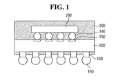
- FIG. 1 is a cross-sectional view of a semiconductor package, according to an exemplary embodiment of the present inventive concept.
- FIG. 2 is a bottom view of a semiconductor package, according to an exemplary embodiment of the present inventive concept.
- FIG. 3 is a cross-sectional view taken along line A-A′ in FIG. 2 .
- a semiconductor package may include a substrate 100 , a vent hole 400 , a semiconductor chip 200 , solder ball pads 150 , and an encapsulant 300 .
- the substrate 100 may be any type of substrate used for semiconductor packaging including, for example, a printed circuit board (PCB) or a ceramic substrate.
- the substrate 100 has an upper surface and a lower surface, which are located on opposing sides of the substrate 100 .
- Connection pads 130 may be formed on the upper surface of the substrate 100 .
- the semiconductor chip 200 may be formed on the upper surface of the substrate 100 , and the solder ball pads 150 may be formed on the lower surface of the substrate 100 .
- the vent hole 400 may be formed on the substrate 100 .
- the vent hole 400 may serve as a path through which the encapsulant 300 passes, as described in further detail below.
- the vent hole 400 may full extend through the substrate 100 .
- the vent hole 400 is formed on the substrate 100 and extends through a portion of the substrate 100 , as shown in FIG. 3 .
- the vent hole 400 is formed such that a liquid material (e.g., encapsulant 300 ) can flow from an area near the upper surface of the substrate 100 to an area near the lower surface of the substrate 100 .
- the vent hole 400 may be formed below the semiconductor chip 200 that is mounted on the upper surface of the substrate 100 , however, the location at which the vent hole 400 is formed is not limited thereto.
- the vent hole may be formed in an area adjacent to the semiconductor chip 200 .
- a void e.g., a bubble
- the vent hole 400 may serve as a path through which the encapsulant 300 passes to remove the void that may be trapped near the lower portion of the semiconductor chip 200 . Removing the void that is trapped near the lower portion of the semiconductor chip 200 may improve the reliability of the semiconductor package.
- the semiconductor chip 200 is mounted on the upper surface of the substrate 100 .
- the semiconductor chip 200 may be mounted at or near the center region of the upper surface of the substrate 100 using an adhesive means such as, for example, liquid epoxy, adhesive tape, or a conductive medium, however the mounting location and the mounting means of the semiconductor chip 200 are not limited thereto.
- Bumps 140 may be formed on the upper surface of the semiconductor chip 200 .
- the bumps 140 of the semiconductor chip 200 may be formed in areas corresponding to the connection pads 130 of the substrate 100 . That is, the semiconductor chip 200 on which the bumps 140 are formed may be mounted on the upper surface of the substrate 100 , and may be electrically connected to the substrate 100 through the bumps 140 .
- the bumps 140 may be formed of, for example, gold, silver, nickel, copper, tin, or an alloy thereof, however the bumps 140 are not limited thereto.
- the bumps 140 may be formed of copper-nickel-lead (Cu—Ni—Pb), copper-nickel-gold (Cu—Ni—Au), copper-nickel (Cu—Ni), Nickel-gold (Ni—Au), or nickel-silver (Ni—Ag).
- FIGS. 1 to 3 show one semiconductor chip 200 included in the semiconductor package, exemplary embodiments of the present inventive concept are not limited thereto.
- the semiconductor package may include one or more additional semiconductor chips, which may be, for example, vertically laminated to the semiconductor chip 200 .
- the solder ball pads 150 may be formed on the lower surface of the substrate 100 .
- the solder ball pads 150 may project further from the lower surface of the substrate 100 than the encapsulant 300 that covers the lower surface of the substrate 100 , as shown in FIGS. 1 and 3 . That is, the height of the formed solder ball pads 150 may be greater than the height of the formed encapsulant 300 that covers the lower surface of the substrate 100 .
- the solder ball pads 150 may not be covered by the encapsulant 300 .
- the entirety of the lower surface of the substrate 100 except for the regions in which the solder ball pads 150 are formed on the lower surface of the substrate 100 , may be covered by the encapsulant 300 .
- the upper surface of the substrate 100 may be described as having a connection region and a non-connection region.
- the connection region refers to all areas of the upper surface of the substrate 100 that contact the bumps 140
- the non-connection region refers to all other areas of the upper surface of the substrate 100 (e.g., all areas that do not contact the bumps 140 ). Together, the connection region and the non-connection region form the entirety of the upper surface of the substrate 100 .
- the lower surface of the substrate 100 may be described as having a connection region that refers to all areas of the lower surface of the substrate 100 that contact the solder ball pads 150 , and a non-connection region that refers to all other areas of the lower surface of the substrate 100 (e.g., all areas that do not contact the solder ball pads 150 ). Together, the connection region and the non-connection region form the entirety of the lower surface of the substrate 100 .
- the solder ball pads 150 may be formed along a large portion of the lower surface of the substrate 100 (e.g., the solder ball pads 150 may be formed in every region of the lower surface of the substrate 100 that is not covered by the encapsulant 300 ).
- the solder ball pads 150 may be formed along the lower surface of the substrate 100 at intervals (e.g., regular intervals) such that large spaces between certain solder ball pads 150 on the lower surface of the substrate 100 may not be present.
- solder ball pads 150 may be utilized for the formation of the solder ball pads 150 , and limitations relating to the solder ball layout (e.g., a reduced number of total solder ball pads 150 ) may be avoided.
- connection terminals 160 may be formed on the solder ball pads 150 .
- the connection terminals 160 may electrically connect the semiconductor package to a module board, a main circuit board, etc.
- the connection terminals 160 may be, for example, solder balls or conductive bumps, however, the connection terminals 160 are not limited thereto.
- the encapsulant 300 is formed such that it covers the entire non-connection region of the upper surface of the substrate 100 , the semiconductor chip 200 , and the entire non-connection region of the lower surface of the substrate 100 .
- the encapsulant 300 is formed such that it fills a space between the semiconductor chip 200 and the substrate 100 therewith and protects the bumps 400 , and may increase an adhesive force between the semiconductor chip 200 and the substrate 100 . Further, the encapsulant 300 may maintain the external appearance of the semiconductor package and may protect the semiconductor chip 200 from external physical impact or moisture.
- the encapsulant 300 Since the encapsulant 300 is formed such that it covers the entire non-connection region of the lower surface of the substrate 100 (e.g., all areas other than those in which the solder ball pads 150 are formed), the encapsulant 300 may be molded on both surfaces of the substrate 100 (e.g., the encapsulate 300 may eliminate empty spaces on both surfaces of the substrate 100 ). As a result, the degree of warping of the substrate 100 may be reduced. As the thickness of the semiconductor package is reduced, the molding thickness may be decreased.
- the encapsulant 300 is molded on both surfaces of the substrate 100 , as opposed to being molded only on the upper surface of the substrate 100 (which may result in warping of the substrate 100 due to the difference in coefficient of thermal expansion between the substrate 100 and the encapsulant 300 ), the degree of warping of the substrate 100 may be reduced.
- the encapsulant 300 may be formed such that a surface height of the encapsulant 300 is greater than or equal to the upper surface of the semiconductor chip 200 , however the surface height of the encapsulant 300 is not limited thereto.
- FIGS. 1 and 3 illustrate the encapsulant 300 formed with a surface height that is greater than the upper surface of the semiconductor chip 200 , exemplary embodiments are not limited thereto.
- the encapsulant 300 may be formed during a molding process using, for example, Epoxy Molding Compound (EMC), silicon resin, polyimide, etc.
- EMC Epoxy Molding Compound
- FIG. 4 is a bottom view of a semiconductor package, according to an exemplary embodiment of the present inventive concept. A description of elements previously described may be omitted.
- the substrate 100 may include a plurality of vent holes 400 to 404 .
- the number of vent holes 400 to 404 is not limited to the five vent holes shown in FIG. 4 .
- exemplary embodiments having a plurality of vent holes may include two to four vent holes or more than five vent holes.
- the plurality of vent holes 400 to 404 may be formed on the substrate 100 such that a liquid material (e.g., encapsulant 300 ) may flow from an area near the upper surface of the substrate 100 to an area near the lower surface of the substrate 100 .
- the plurality of vent holes 400 to 404 may be formed below the semiconductor chip 200 that is mounted on the upper surface of the substrate 100 , however the locations at which the vent holes 400 to 404 are formed are not limited thereto. For example, some or all of the vent holes 400 to 404 may be formed in areas adjacent to the semiconductor chip 200 .
- a void e.g., a bubble
- the vent holes 400 to 404 may serve as a path through which the encapsulant 300 passes to remove the void that may be trapped near the lower portion of the semiconductor chip 200 . Formation of the plurality of vent holes 400 may increase the flow speed of the encapsulant 300 , and may improve the removal efficiency of the void.
- FIG. 5 is a cross-sectional view of a semiconductor package, according to an exemplary embodiment of the present inventive concept. A description of elements previously described may be omitted.
- the solder ball pads 150 may be formed such that they are exposed from the encapsulant 300 that covers the lower surface of the substrate 100 . That is, the height of the formed solder ball pads 150 may be equal to, or about equal to the height of the formed encapsulant 300 that covers the lower surface of the substrate 100 , and the encapsulant does not cover the lower surface of the solder ball pads 150 .
- Forming the solder ball pads 150 such that their height is equal to, or about equal to the height of the formed encapsulant 300 that covers the lower surface of the substrate (as opposed to forming the solder ball pads 150 such that their height is greater than the height of the formed encapsulant 300 ) may reduce the thickness of the semiconductor package.
- the encapsulant 300 flows to the lower surface of the substrate 100 , the entire lower surface of the substrate, except for the regions where the solder ball pads 150 are formed on the lower surface of the substrate 100 , may be covered by the encapsulant 300 .
- the upper surface of the substrate 100 may be described as having a connection region and a non-connection region.
- the connection region refers to all areas of the upper surface of the substrate 100 that contact the bumps 140
- the non-connection region refers to all other areas of the upper surface of the substrate 100 (e.g., all areas that do not contact the bumps 140 ). Together, the connection region and the non-connection region form the entirety of the upper surface of the substrate 100 .
- the lower surface of the substrate 100 may be described as having a connection region that refers to all areas of the lower surface of the substrate 100 that contact the solder ball pads 150 , and a non-connection region that refers to all other areas of the lower surface of the substrate 100 (e.g., all areas that do not contact the solder ball pads 150 ). Together, the connection region and the non-connection region form the entirety of the lower surface of the substrate 100 .
- the solder ball pads 150 When the solder ball pads 150 are formed such that they are exposed from the encapsulant 300 that covers the lower surface of the substrate 100 , the solder ball pads 150 may be formed on a large portion of the lower surface of the substrate 100 (e.g., the solder ball pads 150 may be formed in every region of the lower surface of the substrate 100 that is not covered by the encapsulant 300 ). For example, the solder ball pads 150 may be formed along the lower surface of the substrate 100 at intervals (e.g., regular intervals) such that large spaces between certain solder ball pads 150 on the lower surface of the substrate 100 may not be present.
- intervals e.g., regular intervals
- solder ball pads 150 may be utilized for the formation of the solder ball pads 150 , and limitations relating to the solder ball layout (e.g., a reduced number of total solder ball pads 150 ) can be avoided.
- An organic solder paste (OSP) may be formed on the solder ball pads 150 to prevent oxidation.
- FIG. 6 is a perspective view of a semiconductor package, according to an exemplary embodiment of the present inventive concept. A description of elements previously described may be omitted.
- a plurality of semiconductor chips 200 may be mounted on the upper surface of the substrate 100 .
- the plurality of semiconductor chips 200 may be mounted on the upper surface of the substrate 100 using a predetermined adhesive means such as, for example, liquid epoxy, adhesive tape, or a conductive medium, however the mounting location and the mounting means are not limited thereto.
- Bumps 140 may be formed on the lower surfaces of the plurality of semiconductor chips 200 .
- the bumps 140 on the plurality of semiconductor chips 200 may be formed in areas corresponding to the connection pads 130 of the substrate 100 .
- the plurality of semiconductor chips 200 on which the bumps 140 are formed may be mounted on the upper surface of the substrate 100 , and may be electrically connected to the substrate 100 through the bumps 140 .
- the bumps may be formed of, for example, gold, silver, nickel, copper, tin, or an alloy thereof, however the bumps 140 are not limited thereto.
- the bumps 140 may be formed of copper-nickel-lead (Cu—Ni—Pb), copper-nickel-gold (Cu—Ni—Au), copper-nickel (Cu—Ni), Nickel-gold (Ni—Au), or nickel-silver (Ni—Ag).
- a semiconductor chip 200 is mounted on an upper surface of a substrate 100 on which a vent hole 400 is formed.
- Connection pads 130 may be formed on the upper surface of the substrate 100
- bumps 140 may be formed on the lower surface of the semiconductor chip 200 .
- the semiconductor chip 200 may be mounted such that the bumps 140 and the connection pads 130 are electrically connected to each other.
- solder ball pads 150 are formed on the lower surface of the substrate 100 .
- the solder ball pads 150 may be formed such that they project further from the lower surface of the substrate 100 than an encapsulant 300 that covers the lower surface of the substrate 100 , as described below.
- a release film 500 is formed on the solder ball pads 150 .
- the release film 500 may be formed to have a structure such that the solder ball pads 150 project further from the lower surface of the substrate 100 than the encapsulant 300 that covers the lower surface of the substrate 100 .
- the encapsulant 300 may not cover the solder ball pads 150 when the encapsulant 300 is injected, as described below.
- the encapsulant 300 is injected such that it covers the entire non-connection region of the upper surface of the substrate 100 (e.g., all areas other than those that contact the bumps 140 ), the semiconductor chip 200 , and the entire non-connection region of the lower surface of the substrate 100 (e.g., all areas other than those in which the solder ball pads 150 are formed).
- the encapsulant 300 covers the upper surface of the substrate 100 and the semiconductor chip 200 , and flows to the lower surface of the substrate 100 through the vent hole 400 . After the encapsulant 300 is injected, the encapsulant 300 is hardened.
- the release film 500 is removed. After removing the release film 500 , the solder ball pads 150 have a structure in which the solder ball pads 150 project further from the lower surface of the substrate 100 than the encapsulant 300 that covers the lower surface of the substrate 100 .
- FIG. 12 is a block diagram of an electronic system including the semiconductor device according to exemplary embodiments of the present inventive concept.
- an electronic system 1100 may include a controller 1110 , an input/output (I/O) device 1120 , a memory device 1130 , an interface 1140 , and a bus 1150 .
- the controller 1110 , the I/O device 1120 , the memory device 1130 , and/or the interface 1140 may be coupled to one another through the bus 1150 .
- the bus 1150 corresponds to paths through which data is transferred.
- the controller 1110 may include at least one of, for example, a microprocessor, a digital signal processor, a microcontroller, or logic elements that can perform similar functions.
- the I/O device 1120 may include, for example, a keypad, a keyboard, or a display device.
- the memory device 1130 may store data and/or commands.
- the interface 1140 may transfer the data to a communication network, or receive the data from the communication network.
- the interface 1140 may be wired or wireless.
- the interface 1140 may include an antenna or a wired/wireless transceiver.
- the electronic system 1100 may further include a high-speed DRAM and/or SRAM as an operating memory, which may improve the operation of the controller 1110 .
- Thin film transistors according to some exemplary embodiments of the present inventive concept may be provided inside the memory device 1130 , or may be provided as a part of the controller 1110 and the I/O device 1120 .
- the electronic system 1100 may be, for example, a PDA (Personal Digital Assistant), a portable computer, a web tablet, a wireless phone, a mobile phone, a digital music player, a memory card, or any other type of electronic device that can transmit and/or receive information.
- PDA Personal Digital Assistant
- portable computer a web tablet
- wireless phone a mobile phone
- digital music player a digital music player
- memory card any other type of electronic device that can transmit and/or receive information.
- FIGS. 13 and 14 are exemplary views of a semiconductor system in which the semiconductor device according to exemplary embodiments of the present inventive concept can be applied.
- FIG. 13 illustrates a tablet PC
- FIG. 14 illustrates a notebook PC.
- At least one of the semiconductor devices according to exemplary embodiments of the present inventive concept can be applied to the tablet PC or the notebook PC.
- semiconductor devices according to exemplary embodiments of the present inventive concept may be applied to other integrated circuit devices.
Landscapes
- Structures Or Materials For Encapsulating Or Coating Semiconductor Devices Or Solid State Devices (AREA)
- Engineering & Computer Science (AREA)
- Manufacturing & Machinery (AREA)
Abstract
Description
- This application claims priority under 35 U.S.C. §119 to Korean Patent Application No. 10-2012-0120537, filed on Oct. 29, 2012, the disclosure of which is incorporated by reference herein in its entirety.
- Exemplary embodiments of the present inventive concept relate to a semiconductor package and a method of fabricating the same.
- In a semiconductor package structure, electrical connections between a semiconductor chip and a substrate may be implemented using wire bonding. However, when wire bonding is utilized, wires may be disconnected in the subsequent molding process. Further, due to the length and configuration of the wires, there may be a limit to the degree that the thickness of the package may be reduced.
- As a result, flip chip bonding technology may be used instead of wire bonding to electrically connect the semiconductor chip and the substrate. Utilization of flip chip bonding may reduce electrical signal transfer paths and improve reliability of the semiconductor package.
- According to exemplary embodiments of the present inventive concept, a semiconductor package has a structure that allows for the removal of a void(s) near a lower portion of a semiconductor chip in the semiconductor package.
- According to exemplary embodiments of the present inventive concept, a method of fabricating a semiconductor package allows for the fabrication of a semiconductor package having a structure that allows for the removal of a void(s) near a lower portion of a semiconductor chip in the semiconductor package.
- According to an exemplary embodiment of the present inventive concept, a semiconductor package includes a substrate including a vent hole extending through the substrate, a semiconductor chip mounted on an upper surface of the substrate, a plurality of solder ball pads formed on a lower surface of the substrate, and an encapsulant covering the upper surface of the substrate, the semiconductor chip, and an entirety of the lower surface of the substrate except for regions in which the solder ball pads are formed.
- According to an exemplary embodiment of the present inventive concept, a method of fabricating a semiconductor package includes mounting a semiconductor chip on an upper surface of a substrate, wherein the substrate includes a vent hole extending through the substrate, forming a plurality of solder ball pads on a lower surface of the substrate, and forming an encapsulant, wherein the encapsulant covers the upper surface of the substrate, the semiconductor chip, and an entirety of the lower surface of the substrate except for regions in which the solder ball pads are formed.
- According to an exemplary embodiment of the present inventive concept, a semiconductor package includes a substrate including a vent hole fully extending through the substrate, a semiconductor chip mounted on an upper surface of the substrate, wherein the upper surface includes a first connection region and a first non-connection region forming an entirety of the upper surface, a plurality of connection pads formed on the upper surface of the substrate, a plurality of bumps formed on a lower surface of the semiconductor chip, wherein the plurality of bumps and the plurality of connection pads are electrically connected to each other at the first connection region, a plurality of solder ball pads formed in a second connection region of a lower surface of the substrate, wherein the lower surface opposes the upper surface, and the lower surface comprises the second connection region and a second non-connection region forming an entirety of the lower surface, and an encapsulant covering an entirety of the first and second non-connection regions and the semiconductor chip.
- The above and other features of the present inventive concept will become more apparent by describing in detail exemplary embodiments thereof with reference to the accompanying drawings, in which:
-
FIG. 1 is a cross-sectional view of a semiconductor package, according to an exemplary embodiment of the present inventive concept; -
FIG. 2 is a bottom view of a semiconductor package, according to an exemplary embodiment of the present inventive concept; -
FIG. 3 is a cross-sectional view taken along line A-A′ inFIG. 2 , according to an exemplary embodiment of the present inventive concept; -
FIG. 4 is a bottom view of a semiconductor package, according to an exemplary embodiment of the present inventive concept; -
FIG. 5 is a cross-sectional view of a semiconductor package, according to an exemplary embodiment of the present inventive concept; -
FIG. 6 is a perspective view of a semiconductor package, according to an exemplary embodiment of the present inventive concept; -
FIGS. 7 to 11 are views illustrating a method of fabricating a semiconductor package, according to an exemplary embodiment of the present inventive concept; -
FIG. 12 is a block diagram of an electronic system including a semiconductor device according to exemplary embodiments of the present inventive concept; and -
FIGS. 13 and 14 are exemplary views of a semiconductor system in which the semiconductor device according to exemplary embodiments of the present inventive concept can be applied. - Exemplary embodiments of the present inventive concept will be described more fully hereinafter with reference to the accompanying drawings. Like reference numerals may refer to like elements throughout the accompanying drawings.
- It is understood that when a layer is referred to as being “on” another layer or substrate, it can be directly on the other layer or substrate, or intervening layers may also be present.
- Spatially relative terms, such as “beneath,” “below,” “lower,” “above,” “upper” and the like, may be used herein for ease of description to describe one element or feature's relationship to another element(s) or feature(s) as illustrated in the figures. It is understood that the spatially relative terms are intended to encompass different orientations of the device in use or operation in addition to the orientation depicted in the figures.
- According to exemplary embodiments of the present inventive concept, a semiconductor package and a method of fabricating the same as described hereinafter relate to a semiconductor package having a structure in which a void near a lower portion of a semiconductor chip may be removed. In order to remove the void near the lower portion of the semiconductor chip, a vent hole may exist on a substrate. In a molded underfill (MUF) process, an encapsulant may flow to a lower surface of the substrate through the vent hole on the substrate after covering an upper surface of the substrate and the semiconductor chip. Solder ball pads may be formed in regions of the lower surface of the substrate other than those in which the encapsulant flows.
- Further, in order to reduce the thickness of the semiconductor package, the thickness of molding may be reduced. In an exemplary embodiment, the solder ball pads may be formed on the entire lower surface of the substrate other than areas in which the encapsulant is formed, and the encapsulant may be formed on the entire lower surface of the substrate other than areas in which the solder ball pads are formed.
-
FIG. 1 is a cross-sectional view of a semiconductor package, according to an exemplary embodiment of the present inventive concept.FIG. 2 is a bottom view of a semiconductor package, according to an exemplary embodiment of the present inventive concept.FIG. 3 is a cross-sectional view taken along line A-A′ inFIG. 2 . - Referring to
FIGS. 1 to 3 , a semiconductor package may include asubstrate 100, avent hole 400, asemiconductor chip 200,solder ball pads 150, and an encapsulant 300. - The
substrate 100 may be any type of substrate used for semiconductor packaging including, for example, a printed circuit board (PCB) or a ceramic substrate. Thesubstrate 100 has an upper surface and a lower surface, which are located on opposing sides of thesubstrate 100.Connection pads 130 may be formed on the upper surface of thesubstrate 100. Thesemiconductor chip 200 may be formed on the upper surface of thesubstrate 100, and thesolder ball pads 150 may be formed on the lower surface of thesubstrate 100. Thevent hole 400 may be formed on thesubstrate 100. Thevent hole 400 may serve as a path through which the encapsulant 300 passes, as described in further detail below. Thevent hole 400 may full extend through thesubstrate 100. - The
vent hole 400 is formed on thesubstrate 100 and extends through a portion of thesubstrate 100, as shown inFIG. 3 . Thevent hole 400 is formed such that a liquid material (e.g., encapsulant 300) can flow from an area near the upper surface of thesubstrate 100 to an area near the lower surface of thesubstrate 100. Thevent hole 400 may be formed below thesemiconductor chip 200 that is mounted on the upper surface of thesubstrate 100, however, the location at which thevent hole 400 is formed is not limited thereto. For example, the vent hole may be formed in an area adjacent to thesemiconductor chip 200. When theencapsulant 300 is injected during a molding process, a void (e.g., a bubble) may occur. When a void occurs, thevent hole 400 may serve as a path through which the encapsulant 300 passes to remove the void that may be trapped near the lower portion of thesemiconductor chip 200. Removing the void that is trapped near the lower portion of thesemiconductor chip 200 may improve the reliability of the semiconductor package. - The
semiconductor chip 200 is mounted on the upper surface of thesubstrate 100. Thesemiconductor chip 200 may be mounted at or near the center region of the upper surface of thesubstrate 100 using an adhesive means such as, for example, liquid epoxy, adhesive tape, or a conductive medium, however the mounting location and the mounting means of thesemiconductor chip 200 are not limited thereto.Bumps 140 may be formed on the upper surface of thesemiconductor chip 200. For example, thebumps 140 of thesemiconductor chip 200 may be formed in areas corresponding to theconnection pads 130 of thesubstrate 100. That is, thesemiconductor chip 200 on which thebumps 140 are formed may be mounted on the upper surface of thesubstrate 100, and may be electrically connected to thesubstrate 100 through thebumps 140. Thebumps 140 may be formed of, for example, gold, silver, nickel, copper, tin, or an alloy thereof, however thebumps 140 are not limited thereto. For example, thebumps 140 may be formed of copper-nickel-lead (Cu—Ni—Pb), copper-nickel-gold (Cu—Ni—Au), copper-nickel (Cu—Ni), Nickel-gold (Ni—Au), or nickel-silver (Ni—Ag). - Although
FIGS. 1 to 3 show onesemiconductor chip 200 included in the semiconductor package, exemplary embodiments of the present inventive concept are not limited thereto. For example, the semiconductor package may include one or more additional semiconductor chips, which may be, for example, vertically laminated to thesemiconductor chip 200. - The
solder ball pads 150 may be formed on the lower surface of thesubstrate 100. Thesolder ball pads 150 may project further from the lower surface of thesubstrate 100 than theencapsulant 300 that covers the lower surface of thesubstrate 100, as shown inFIGS. 1 and 3 . That is, the height of the formedsolder ball pads 150 may be greater than the height of the formedencapsulant 300 that covers the lower surface of thesubstrate 100. When theencapsulant 300 flows to the lower surface of thesubstrate 100, thesolder ball pads 150 may not be covered by theencapsulant 300. As a result, the entirety of the lower surface of thesubstrate 100, except for the regions in which thesolder ball pads 150 are formed on the lower surface of thesubstrate 100, may be covered by theencapsulant 300. - The upper surface of the
substrate 100 may be described as having a connection region and a non-connection region. The connection region refers to all areas of the upper surface of thesubstrate 100 that contact thebumps 140, and the non-connection region refers to all other areas of the upper surface of the substrate 100 (e.g., all areas that do not contact the bumps 140). Together, the connection region and the non-connection region form the entirety of the upper surface of thesubstrate 100. Similarly, the lower surface of thesubstrate 100 may be described as having a connection region that refers to all areas of the lower surface of thesubstrate 100 that contact thesolder ball pads 150, and a non-connection region that refers to all other areas of the lower surface of the substrate 100 (e.g., all areas that do not contact the solder ball pads 150). Together, the connection region and the non-connection region form the entirety of the lower surface of thesubstrate 100. - When the
solder ball pads 150 project further than theencapsulant 300 that covers the lower surface of thesubstrate 100, thesolder ball pads 150 may be formed along a large portion of the lower surface of the substrate 100 (e.g., thesolder ball pads 150 may be formed in every region of the lower surface of thesubstrate 100 that is not covered by the encapsulant 300). For example, thesolder ball pads 150 may be formed along the lower surface of thesubstrate 100 at intervals (e.g., regular intervals) such that large spaces between certainsolder ball pads 150 on the lower surface of thesubstrate 100 may not be present. As a result, a large portion of the lower surface of thesubstrate 100 may be utilized for the formation of thesolder ball pads 150, and limitations relating to the solder ball layout (e.g., a reduced number of total solder ball pads 150) may be avoided. - To prevent oxidation, an organic solder paste (OSP) may be formed on the
solder ball pads 150. Further,connection terminals 160 may be formed on thesolder ball pads 150. Theconnection terminals 160 may electrically connect the semiconductor package to a module board, a main circuit board, etc. Theconnection terminals 160 may be, for example, solder balls or conductive bumps, however, theconnection terminals 160 are not limited thereto. - The
encapsulant 300 is formed such that it covers the entire non-connection region of the upper surface of thesubstrate 100, thesemiconductor chip 200, and the entire non-connection region of the lower surface of thesubstrate 100. Theencapsulant 300 is formed such that it fills a space between thesemiconductor chip 200 and thesubstrate 100 therewith and protects thebumps 400, and may increase an adhesive force between thesemiconductor chip 200 and thesubstrate 100. Further, theencapsulant 300 may maintain the external appearance of the semiconductor package and may protect thesemiconductor chip 200 from external physical impact or moisture. Since theencapsulant 300 is formed such that it covers the entire non-connection region of the lower surface of the substrate 100 (e.g., all areas other than those in which thesolder ball pads 150 are formed), theencapsulant 300 may be molded on both surfaces of the substrate 100 (e.g., theencapsulate 300 may eliminate empty spaces on both surfaces of the substrate 100). As a result, the degree of warping of thesubstrate 100 may be reduced. As the thickness of the semiconductor package is reduced, the molding thickness may be decreased. According to exemplary embodiments, since theencapsulant 300 is molded on both surfaces of thesubstrate 100, as opposed to being molded only on the upper surface of the substrate 100 (which may result in warping of thesubstrate 100 due to the difference in coefficient of thermal expansion between thesubstrate 100 and the encapsulant 300), the degree of warping of thesubstrate 100 may be reduced. - According to exemplary embodiments, the
encapsulant 300 may be formed such that a surface height of theencapsulant 300 is greater than or equal to the upper surface of thesemiconductor chip 200, however the surface height of theencapsulant 300 is not limited thereto. For example, althoughFIGS. 1 and 3 illustrate theencapsulant 300 formed with a surface height that is greater than the upper surface of thesemiconductor chip 200, exemplary embodiments are not limited thereto. Theencapsulant 300 may be formed during a molding process using, for example, Epoxy Molding Compound (EMC), silicon resin, polyimide, etc. -
FIG. 4 is a bottom view of a semiconductor package, according to an exemplary embodiment of the present inventive concept. A description of elements previously described may be omitted. - Referring to
FIG. 4 , in a semiconductor package according to an exemplary embodiment of the present inventive concept, thesubstrate 100 may include a plurality of vent holes 400 to 404. The number of vent holes 400 to 404 is not limited to the five vent holes shown inFIG. 4 . For example, exemplary embodiments having a plurality of vent holes may include two to four vent holes or more than five vent holes. The plurality of vent holes 400 to 404 may be formed on thesubstrate 100 such that a liquid material (e.g., encapsulant 300) may flow from an area near the upper surface of thesubstrate 100 to an area near the lower surface of thesubstrate 100. The plurality of vent holes 400 to 404 may be formed below thesemiconductor chip 200 that is mounted on the upper surface of thesubstrate 100, however the locations at which the vent holes 400 to 404 are formed are not limited thereto. For example, some or all of the vent holes 400 to 404 may be formed in areas adjacent to thesemiconductor chip 200. When theencapsulant 300 is injected during the molding process, a void (e.g., a bubble) may occur. When a void occurs, the vent holes 400 to 404 may serve as a path through which theencapsulant 300 passes to remove the void that may be trapped near the lower portion of thesemiconductor chip 200. Formation of the plurality of vent holes 400 may increase the flow speed of theencapsulant 300, and may improve the removal efficiency of the void. -
FIG. 5 is a cross-sectional view of a semiconductor package, according to an exemplary embodiment of the present inventive concept. A description of elements previously described may be omitted. - Referring to
FIG. 5 , in a semiconductor package according to an exemplary embodiment of the present inventive concept, thesolder ball pads 150 may be formed such that they are exposed from theencapsulant 300 that covers the lower surface of thesubstrate 100. That is, the height of the formedsolder ball pads 150 may be equal to, or about equal to the height of the formedencapsulant 300 that covers the lower surface of thesubstrate 100, and the encapsulant does not cover the lower surface of thesolder ball pads 150. Forming thesolder ball pads 150 such that their height is equal to, or about equal to the height of the formedencapsulant 300 that covers the lower surface of the substrate (as opposed to forming thesolder ball pads 150 such that their height is greater than the height of the formed encapsulant 300) may reduce the thickness of the semiconductor package. When theencapsulant 300 flows to the lower surface of thesubstrate 100, the entire lower surface of the substrate, except for the regions where thesolder ball pads 150 are formed on the lower surface of thesubstrate 100, may be covered by theencapsulant 300. - The upper surface of the
substrate 100 may be described as having a connection region and a non-connection region. The connection region refers to all areas of the upper surface of thesubstrate 100 that contact thebumps 140, and the non-connection region refers to all other areas of the upper surface of the substrate 100 (e.g., all areas that do not contact the bumps 140). Together, the connection region and the non-connection region form the entirety of the upper surface of thesubstrate 100. Similarly, the lower surface of thesubstrate 100 may be described as having a connection region that refers to all areas of the lower surface of thesubstrate 100 that contact thesolder ball pads 150, and a non-connection region that refers to all other areas of the lower surface of the substrate 100 (e.g., all areas that do not contact the solder ball pads 150). Together, the connection region and the non-connection region form the entirety of the lower surface of thesubstrate 100. - When the
solder ball pads 150 are formed such that they are exposed from theencapsulant 300 that covers the lower surface of thesubstrate 100, thesolder ball pads 150 may be formed on a large portion of the lower surface of the substrate 100 (e.g., thesolder ball pads 150 may be formed in every region of the lower surface of thesubstrate 100 that is not covered by the encapsulant 300). For example, thesolder ball pads 150 may be formed along the lower surface of thesubstrate 100 at intervals (e.g., regular intervals) such that large spaces between certainsolder ball pads 150 on the lower surface of thesubstrate 100 may not be present. As a result, a large portion of the lower surface of thesubstrate 100 may be utilized for the formation of thesolder ball pads 150, and limitations relating to the solder ball layout (e.g., a reduced number of total solder ball pads 150) can be avoided. An organic solder paste (OSP) may be formed on thesolder ball pads 150 to prevent oxidation. -
FIG. 6 is a perspective view of a semiconductor package, according to an exemplary embodiment of the present inventive concept. A description of elements previously described may be omitted. - Referring to
FIG. 6 , in a semiconductor package according to an exemplary embodiment of the present inventive concept, a plurality ofsemiconductor chips 200 may be mounted on the upper surface of thesubstrate 100. The plurality ofsemiconductor chips 200 may be mounted on the upper surface of thesubstrate 100 using a predetermined adhesive means such as, for example, liquid epoxy, adhesive tape, or a conductive medium, however the mounting location and the mounting means are not limited thereto.Bumps 140 may be formed on the lower surfaces of the plurality ofsemiconductor chips 200. For example, thebumps 140 on the plurality ofsemiconductor chips 200 may be formed in areas corresponding to theconnection pads 130 of thesubstrate 100. That is, the plurality ofsemiconductor chips 200 on which thebumps 140 are formed may be mounted on the upper surface of thesubstrate 100, and may be electrically connected to thesubstrate 100 through thebumps 140. The bumps may be formed of, for example, gold, silver, nickel, copper, tin, or an alloy thereof, however thebumps 140 are not limited thereto. For example, thebumps 140 may be formed of copper-nickel-lead (Cu—Ni—Pb), copper-nickel-gold (Cu—Ni—Au), copper-nickel (Cu—Ni), Nickel-gold (Ni—Au), or nickel-silver (Ni—Ag). - Hereinafter, a method of fabricating a semiconductor package according to an exemplary embodiment of the present inventive concept will be described with reference to
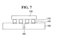
FIGS. 7 to 11 . - Referring to
FIG. 7 , asemiconductor chip 200 is mounted on an upper surface of asubstrate 100 on which avent hole 400 is formed.Connection pads 130 may be formed on the upper surface of thesubstrate 100, and bumps 140 may be formed on the lower surface of thesemiconductor chip 200. Thesemiconductor chip 200 may be mounted such that thebumps 140 and theconnection pads 130 are electrically connected to each other. - Referring to
FIG. 8 ,solder ball pads 150 are formed on the lower surface of thesubstrate 100. Thesolder ball pads 150 may be formed such that they project further from the lower surface of thesubstrate 100 than anencapsulant 300 that covers the lower surface of thesubstrate 100, as described below. - Referring to
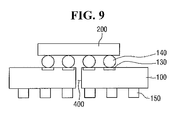
FIG. 9 , arelease film 500 is formed on thesolder ball pads 150. Therelease film 500 may be formed to have a structure such that thesolder ball pads 150 project further from the lower surface of thesubstrate 100 than theencapsulant 300 that covers the lower surface of thesubstrate 100. As a result of the presence of therelease film 500, theencapsulant 300 may not cover thesolder ball pads 150 when theencapsulant 300 is injected, as described below. - Referring to
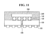
FIG. 10 , theencapsulant 300 is injected such that it covers the entire non-connection region of the upper surface of the substrate 100 (e.g., all areas other than those that contact the bumps 140), thesemiconductor chip 200, and the entire non-connection region of the lower surface of the substrate 100 (e.g., all areas other than those in which thesolder ball pads 150 are formed). Theencapsulant 300 covers the upper surface of thesubstrate 100 and thesemiconductor chip 200, and flows to the lower surface of thesubstrate 100 through thevent hole 400. After theencapsulant 300 is injected, theencapsulant 300 is hardened. - Referring to
FIG. 11 , therelease film 500 is removed. After removing therelease film 500, thesolder ball pads 150 have a structure in which thesolder ball pads 150 project further from the lower surface of thesubstrate 100 than theencapsulant 300 that covers the lower surface of thesubstrate 100. -
FIG. 12 is a block diagram of an electronic system including the semiconductor device according to exemplary embodiments of the present inventive concept. - Referring to
FIG. 12 , anelectronic system 1100 according to an exemplary embodiment of the present inventive concept may include acontroller 1110, an input/output (I/O)device 1120, amemory device 1130, aninterface 1140, and abus 1150. Thecontroller 1110, the I/O device 1120, thememory device 1130, and/or theinterface 1140 may be coupled to one another through thebus 1150. Thebus 1150 corresponds to paths through which data is transferred. - The
controller 1110 may include at least one of, for example, a microprocessor, a digital signal processor, a microcontroller, or logic elements that can perform similar functions. The I/O device 1120 may include, for example, a keypad, a keyboard, or a display device. Thememory device 1130 may store data and/or commands. Theinterface 1140 may transfer the data to a communication network, or receive the data from the communication network. Theinterface 1140 may be wired or wireless. For example, theinterface 1140 may include an antenna or a wired/wireless transceiver. Theelectronic system 1100 may further include a high-speed DRAM and/or SRAM as an operating memory, which may improve the operation of thecontroller 1110. Thin film transistors according to some exemplary embodiments of the present inventive concept may be provided inside thememory device 1130, or may be provided as a part of thecontroller 1110 and the I/O device 1120. - The
electronic system 1100 may be, for example, a PDA (Personal Digital Assistant), a portable computer, a web tablet, a wireless phone, a mobile phone, a digital music player, a memory card, or any other type of electronic device that can transmit and/or receive information. -
FIGS. 13 and 14 are exemplary views of a semiconductor system in which the semiconductor device according to exemplary embodiments of the present inventive concept can be applied.FIG. 13 illustrates a tablet PC, andFIG. 14 illustrates a notebook PC. At least one of the semiconductor devices according to exemplary embodiments of the present inventive concept can be applied to the tablet PC or the notebook PC. In addition, semiconductor devices according to exemplary embodiments of the present inventive concept may be applied to other integrated circuit devices. - While the present inventive concept has been particularly shown and described with reference to the exemplary embodiments thereof, it will be understood by those skilled in the art that various changes in form and detail may be made therein without departing from the spirit and scope of the present inventive concept as defined by the following claims.
Claims (20)
Applications Claiming Priority (2)
| Application Number | Priority Date | Filing Date | Title |
|---|---|---|---|
| KR1020120120537A KR101965127B1 (en) | 2012-10-29 | 2012-10-29 | Semiconductor package and method for fabricating the same |
| KR10-2012-0120537 | 2012-10-29 |
Publications (2)
| Publication Number | Publication Date |
|---|---|
| US20140117543A1 true US20140117543A1 (en) | 2014-05-01 |
| US9236337B2 US9236337B2 (en) | 2016-01-12 |
Family
ID=50546287
Family Applications (1)
| Application Number | Title | Priority Date | Filing Date |
|---|---|---|---|
| US13/950,669 Active 2033-08-02 US9236337B2 (en) | 2012-10-29 | 2013-07-25 | Semiconductor package including a substrate having a vent hole |
Country Status (2)
| Country | Link |
|---|---|
| US (1) | US9236337B2 (en) |
| KR (1) | KR101965127B1 (en) |
Cited By (2)
| Publication number | Priority date | Publication date | Assignee | Title |
|---|---|---|---|---|
| US20150262956A1 (en) * | 2014-03-14 | 2015-09-17 | Taiwan Semiconductor Manufacturing Company, Ltd. | Package Substrates, Packaged Semiconductor Devices, and Methods of Packaging Semiconductor Devices |
| US20220351984A1 (en) * | 2020-02-19 | 2022-11-03 | Changxin Memory Technologies, Inc. | Package substrate and method of forming the same, package structure and method of forming the same |
Citations (2)
| Publication number | Priority date | Publication date | Assignee | Title |
|---|---|---|---|---|
| US7307347B2 (en) * | 2000-03-13 | 2007-12-11 | Dai Nippon Printing Co., Ltd. | Resin-encapsulated package, lead member for the same and method of fabricating the lead member |
| US7568922B2 (en) * | 2004-12-17 | 2009-08-04 | Ibiden Co., Ltd. | Printed wiring board having a solder pad and a method for manufacturing the same |
Family Cites Families (30)
| Publication number | Priority date | Publication date | Assignee | Title |
|---|---|---|---|---|
| US6038136A (en) | 1997-10-29 | 2000-03-14 | Hestia Technologies, Inc. | Chip package with molded underfill |
| KR100299384B1 (en) | 1998-12-16 | 2001-10-29 | 박종섭 | Ball grid array package |
| KR100575859B1 (en) | 1999-06-18 | 2006-05-03 | 주식회사 하이닉스반도체 | Ball grid array package |
| KR100333386B1 (en) | 1999-06-29 | 2002-04-18 | 박종섭 | chip scale package |
| KR100679816B1 (en) | 2001-01-03 | 2007-02-07 | 앰코 테크놀로지 코리아 주식회사 | Semiconductor package |
| KR100691942B1 (en) | 2001-01-15 | 2007-03-08 | 앰코 테크놀로지 코리아 주식회사 | Semiconductor package and manufacturing method thereof |
| JP2006165324A (en) | 2004-12-08 | 2006-06-22 | Toyota Motor Corp | Substrate structure with BGA package mounted |
| KR20080029706A (en) * | 2006-09-29 | 2008-04-03 | 주식회사 하이닉스반도체 | Semiconductor package |
| US8063474B2 (en) | 2008-02-06 | 2011-11-22 | Fairchild Semiconductor Corporation | Embedded die package on package (POP) with pre-molded leadframe |
| US8310051B2 (en) | 2008-05-27 | 2012-11-13 | Mediatek Inc. | Package-on-package with fan-out WLCSP |
| US8076180B2 (en) | 2008-07-07 | 2011-12-13 | Infineon Technologies Ag | Repairable semiconductor device and method |
| US8039938B2 (en) | 2009-05-22 | 2011-10-18 | Palo Alto Research Center Incorporated | Airgap micro-spring interconnect with bonded underfill seal |
| US8034660B2 (en) | 2009-07-24 | 2011-10-11 | Texas Instruments Incorporated | PoP precursor with interposer for top package bond pad pitch compensation |
| KR20110092045A (en) * | 2010-02-08 | 2011-08-17 | 삼성전자주식회사 | Molded underfill flip chip package suppresses warpage and voids |
| WO2011140469A1 (en) | 2010-05-06 | 2011-11-10 | Zakaryae Fathi | Adhesive bonding composition and method of use |
| US20110309481A1 (en) | 2010-06-18 | 2011-12-22 | Rui Huang | Integrated circuit packaging system with flip chip mounting and method of manufacture thereof |
| US8273607B2 (en) | 2010-06-18 | 2012-09-25 | Stats Chippac Ltd. | Integrated circuit packaging system with encapsulation and underfill and method of manufacture thereof |
| US8264849B2 (en) | 2010-06-23 | 2012-09-11 | Intel Corporation | Mold compounds in improved embedded-die coreless substrates, and processes of forming same |
| US8502377B2 (en) | 2010-08-06 | 2013-08-06 | Mediatek Inc. | Package substrate for bump on trace interconnection |
| US8435835B2 (en) | 2010-09-02 | 2013-05-07 | Stats Chippac, Ltd. | Semiconductor device and method of forming base leads from base substrate as standoff for stacking semiconductor die |
| US8409918B2 (en) | 2010-09-03 | 2013-04-02 | Stats Chippac, Ltd. | Semiconductor device and method of forming pre-molded substrate to reduce warpage during die mounting |
| US8435834B2 (en) | 2010-09-13 | 2013-05-07 | Stats Chippac, Ltd. | Semiconductor device and method of forming bond-on-lead interconnection for mounting semiconductor die in FO-WLCSP |
| US8193036B2 (en) | 2010-09-14 | 2012-06-05 | Stats Chippac, Ltd. | Semiconductor device and method of forming mold underfill using dispensing needle having same width as semiconductor die |
| US8399305B2 (en) | 2010-09-20 | 2013-03-19 | Stats Chippac, Ltd. | Semiconductor device and method of forming dam material with openings around semiconductor die for mold underfill using dispenser and vacuum assist |
| US8313982B2 (en) | 2010-09-20 | 2012-11-20 | Texas Instruments Incorporated | Stacked die assemblies including TSV die |
| US8993377B2 (en) | 2010-09-29 | 2015-03-31 | Stats Chippac, Ltd. | Semiconductor device and method of bonding different size semiconductor die at the wafer level |
| US8338945B2 (en) | 2010-10-26 | 2012-12-25 | Taiwan Semiconductor Manufacturing Company, Ltd. | Molded chip interposer structure and methods |
| JP2012109437A (en) | 2010-11-18 | 2012-06-07 | Elpida Memory Inc | Semiconductor device and method of manufacturing the same |
| US8456021B2 (en) | 2010-11-24 | 2013-06-04 | Texas Instruments Incorporated | Integrated circuit device having die bonded to the polymer side of a polymer substrate |
| KR20120062457A (en) * | 2010-12-06 | 2012-06-14 | 삼성전자주식회사 | Print circuit board for semiconductor package improving a solder joint reliablity and semiconductor package having the same |
-
2012
- 2012-10-29 KR KR1020120120537A patent/KR101965127B1/en active Active
-
2013
- 2013-07-25 US US13/950,669 patent/US9236337B2/en active Active
Patent Citations (2)
| Publication number | Priority date | Publication date | Assignee | Title |
|---|---|---|---|---|
| US7307347B2 (en) * | 2000-03-13 | 2007-12-11 | Dai Nippon Printing Co., Ltd. | Resin-encapsulated package, lead member for the same and method of fabricating the lead member |
| US7568922B2 (en) * | 2004-12-17 | 2009-08-04 | Ibiden Co., Ltd. | Printed wiring board having a solder pad and a method for manufacturing the same |
Cited By (5)
| Publication number | Priority date | Publication date | Assignee | Title |
|---|---|---|---|---|
| US20150262956A1 (en) * | 2014-03-14 | 2015-09-17 | Taiwan Semiconductor Manufacturing Company, Ltd. | Package Substrates, Packaged Semiconductor Devices, and Methods of Packaging Semiconductor Devices |
| US9917068B2 (en) * | 2014-03-14 | 2018-03-13 | Taiwan Semiconductor Manufacturing Company | Package substrates, packaged semiconductor devices, and methods of packaging semiconductor devices |
| US10128208B2 (en) | 2014-03-14 | 2018-11-13 | Taiwan Semiconductor Manufacturing Company | Package substrates, packaged semiconductor devices, and methods of packaging semiconductor devices |
| US20220351984A1 (en) * | 2020-02-19 | 2022-11-03 | Changxin Memory Technologies, Inc. | Package substrate and method of forming the same, package structure and method of forming the same |
| US12027379B2 (en) * | 2020-02-19 | 2024-07-02 | Changxin Memory Technologies, Inc. | Package substrate and method of forming the same, package structure and method of forming the same |
Also Published As
| Publication number | Publication date |
|---|---|
| KR101965127B1 (en) | 2019-04-04 |
| US9236337B2 (en) | 2016-01-12 |
| KR20140054716A (en) | 2014-05-09 |
Similar Documents
| Publication | Publication Date | Title |
|---|---|---|
| US9583430B2 (en) | Package-on-package device | |
| KR102157551B1 (en) | A semiconductor package and method of fabricating the same | |
| US9425156B2 (en) | Semiconductor packages having semiconductor chips disposed in opening in shielding core plate | |
| KR101695846B1 (en) | Stacked semiconductor packages | |
| KR101801945B1 (en) | Semiconductor chip and semiconductor package having the same | |
| KR102214512B1 (en) | Printed circuit board and semiconductor package using the same | |
| US8981543B2 (en) | Semiconductor package and method of forming the same | |
| KR20110083969A (en) | Semiconductor package and manufacturing method thereof | |
| CN102456663B (en) | Semiconductor device and manufacture method thereof | |
| US9373574B2 (en) | Semiconductor packages and methods of forming the same | |
| KR20110055299A (en) | Semiconductor Package with Multi Pitch Ball Lands | |
| US7180166B2 (en) | Stacked multi-chip package | |
| KR20110128748A (en) | Integrated circuit packaging system with double side connections and manufacturing method thereof | |
| KR20160056378A (en) | Semiconductor packages and methods for fabricating the same | |
| KR102216195B1 (en) | Semiconductor package on which a plurality of chips are stacked | |
| KR20150021786A (en) | Semiconductor package | |
| KR20150050798A (en) | semiconductor package and manufacturing method of the same | |
| US20100029046A1 (en) | Integrated circuit package system with concave terminal | |
| US12148729B2 (en) | Semiconductor package structure having interposer substrate, and stacked semiconductor package structure including the same | |
| KR20160022457A (en) | Semiconductor packages | |
| US20140374901A1 (en) | Semiconductor package and method of fabricating the same | |
| KR102190390B1 (en) | Semiconductor package and method of fabricating the same | |
| US9236337B2 (en) | Semiconductor package including a substrate having a vent hole | |
| KR20140130921A (en) | Semiconductor package and method of manufacturing the same | |
| US8828795B2 (en) | Method of fabricating semiconductor package having substrate with solder ball connections |
Legal Events
| Date | Code | Title | Description |
|---|---|---|---|
| AS | Assignment |
Owner name: SAMSUNG ELECTRONICS CO., LTD., KOREA, REPUBLIC OF Free format text: ASSIGNMENT OF ASSIGNORS INTEREST;ASSIGNOR:PARK, CHAN;REEL/FRAME:030876/0753 Effective date: 20130723 |
|
| STCF | Information on status: patent grant |
Free format text: PATENTED CASE |
|
| MAFP | Maintenance fee payment |
Free format text: PAYMENT OF MAINTENANCE FEE, 4TH YEAR, LARGE ENTITY (ORIGINAL EVENT CODE: M1551); ENTITY STATUS OF PATENT OWNER: LARGE ENTITY Year of fee payment: 4 |
|
| MAFP | Maintenance fee payment |
Free format text: PAYMENT OF MAINTENANCE FEE, 8TH YEAR, LARGE ENTITY (ORIGINAL EVENT CODE: M1552); ENTITY STATUS OF PATENT OWNER: LARGE ENTITY Year of fee payment: 8 |