US20120249782A1 - Image capturing device and image capturing method - Google Patents
Image capturing device and image capturing method Download PDFInfo
- Publication number
- US20120249782A1 US20120249782A1 US13/431,543 US201213431543A US2012249782A1 US 20120249782 A1 US20120249782 A1 US 20120249782A1 US 201213431543 A US201213431543 A US 201213431543A US 2012249782 A1 US2012249782 A1 US 2012249782A1
- Authority
- US
- United States
- Prior art keywords
- frame images
- period
- light source
- images captured
- camera
- Prior art date
- Legal status (The legal status is an assumption and is not a legal conclusion. Google has not performed a legal analysis and makes no representation as to the accuracy of the status listed.)
- Granted
Links
Images


Classifications
-
- G—PHYSICS
- G01—MEASURING; TESTING
- G01N—INVESTIGATING OR ANALYSING MATERIALS BY DETERMINING THEIR CHEMICAL OR PHYSICAL PROPERTIES
- G01N21/00—Investigating or analysing materials by the use of optical means, i.e. using sub-millimetre waves, infrared, visible or ultraviolet light
- G01N21/17—Systems in which incident light is modified in accordance with the properties of the material investigated
- G01N21/25—Colour; Spectral properties, i.e. comparison of effect of material on the light at two or more different wavelengths or wavelength bands
- G01N21/31—Investigating relative effect of material at wavelengths characteristic of specific elements or molecules, e.g. atomic absorption spectrometry
- G01N21/35—Investigating relative effect of material at wavelengths characteristic of specific elements or molecules, e.g. atomic absorption spectrometry using infrared light
- G01N21/3581—Investigating relative effect of material at wavelengths characteristic of specific elements or molecules, e.g. atomic absorption spectrometry using infrared light using far infrared light; using Terahertz radiation
- G01N21/3586—Investigating relative effect of material at wavelengths characteristic of specific elements or molecules, e.g. atomic absorption spectrometry using infrared light using far infrared light; using Terahertz radiation by Terahertz time domain spectroscopy [THz-TDS]
-
- G—PHYSICS
- G03—PHOTOGRAPHY; CINEMATOGRAPHY; ANALOGOUS TECHNIQUES USING WAVES OTHER THAN OPTICAL WAVES; ELECTROGRAPHY; HOLOGRAPHY
- G03B—APPARATUS OR ARRANGEMENTS FOR TAKING PHOTOGRAPHS OR FOR PROJECTING OR VIEWING THEM; APPARATUS OR ARRANGEMENTS EMPLOYING ANALOGOUS TECHNIQUES USING WAVES OTHER THAN OPTICAL WAVES; ACCESSORIES THEREFOR
- G03B15/00—Special procedures for taking photographs; Apparatus therefor
- G03B15/02—Illuminating scene
- G03B15/03—Combinations of cameras with lighting apparatus; Flash units
- G03B15/05—Combinations of cameras with electronic flash apparatus; Electronic flash units
-
- G—PHYSICS
- G03—PHOTOGRAPHY; CINEMATOGRAPHY; ANALOGOUS TECHNIQUES USING WAVES OTHER THAN OPTICAL WAVES; ELECTROGRAPHY; HOLOGRAPHY
- G03B—APPARATUS OR ARRANGEMENTS FOR TAKING PHOTOGRAPHS OR FOR PROJECTING OR VIEWING THEM; APPARATUS OR ARRANGEMENTS EMPLOYING ANALOGOUS TECHNIQUES USING WAVES OTHER THAN OPTICAL WAVES; ACCESSORIES THEREFOR
- G03B42/00—Obtaining records using waves other than optical waves; Visualisation of such records by using optical means
-
- G—PHYSICS
- G03—PHOTOGRAPHY; CINEMATOGRAPHY; ANALOGOUS TECHNIQUES USING WAVES OTHER THAN OPTICAL WAVES; ELECTROGRAPHY; HOLOGRAPHY
- G03B—APPARATUS OR ARRANGEMENTS FOR TAKING PHOTOGRAPHS OR FOR PROJECTING OR VIEWING THEM; APPARATUS OR ARRANGEMENTS EMPLOYING ANALOGOUS TECHNIQUES USING WAVES OTHER THAN OPTICAL WAVES; ACCESSORIES THEREFOR
- G03B2215/00—Special procedures for taking photographs; Apparatus therefor
- G03B2215/05—Combinations of cameras with electronic flash units
Definitions
- the present invention relates to an image capturing device that is provided with a light source and a camera and in which a measurement subject is placed in an optical path that lies therebetween, in particular, to an image capturing device that captures an image of a measurement subject in synchronization with ON/OFF states of the light source.
- Image capturing devices that are provided with a light source and a camera and in which a measurement subject is placed in an optical path that lies therebetween are known.
- image capturing devices when an image of a measurement subject is captured in synchronization with the ON/OFF states of the light source (so-called lock-in image capturing), not only images caused by radiations other than the light source can be eliminated, but also low-frequency noises such as 1/f noises can be set to the off setting.
- Non-patent Literature 1 A. W. M. Lee et al., IEEE PHOTONICS TECHNOLOGY LETTERS, VOL 18, NO. 13, Jul. 1, 2006, p. 1415-1417
- a THz wave emitted by a THz light source that is periodically turned ON and OFF is transmitted to a camera whose sensitivity is within a range from the infrared region to the THz (terahertz) region
- the camera detects an electromagnetic wave in which infrared and a periodic THz wave have been mixed and captures an image based on the detected electromagnetic wave.
- infrared images can be set off and thereby only THz images can be obtained.
- a filter that suppresses infrared waves and passes through only THz waves can be omitted.
- FIG. 1 A specific arrangement of the foregoing image capturing device is shown in FIG. 1 .
- light of a THz wave at a frequency of 4.3 THz is emitted by QCL (Quantum Cascade Laser) 102 that is mounted on cooler 101 .
- QCL Quantum Cascade Laser
- the light travels to off-axis parabolic mirror 103 .
- Off-axis parabolic minor 103 collimates the light and reflects the collimated light to off-axis parabolic mirror 104 .
- Off-axis parabolic mirror 104 radiates the collimated light to envelop (measurement subject) 105 .
- microbolometer array sensor 108 that has 320 ⁇ 240 pixels and that is mounted on microbolometer camera 107 (at a frame rate of 60 Hz).
- Microbolometer array sensor 108 captures an image based on the collected light of the THz wave.
- FIG. 2 shows a lock-in image capturing method for the image capturing device shown in FIG. 1 .
- QCL 102 is turned ON at frame 1 and QCL 102 is turned OFF at frame 2 and frame 3.
- an infrared wave and THz wave emitted by QCL 102 are collected to microbolometer array sensor 108 and thereby an image is captured based on both the infrared and THz wave, whereas at frame 2 and frame 3, only infrared waves are collected to microbolometer array sensor 108 and thereby an image is captured based on only the infrared.
- a THz image can be obtained as an image captured based on only the THz wave emitted by QCL 102 .
- Frame 2 is not used in order to increase the difference between image data of frame 1 and image data of frame 3 since a sufficiently long time elapses after the image data of frame 1 has been captured compared to a thermal time constant of around 13 msec of microbolometer array sensor 108 .
- FIG. 3 shows THz image 110 that is captured from envelop 105 that contains paper 109 with letters “MIT” written with a pencil at a frame rate of 20 Hz based on the method shown in FIG. 2 .
- letters “MIT” can be checked out without necessity of opening envelop 105 .
- an object of the present invention is to provide an image capturing device and an image capturing method that can solve the foregoing problem.
- a first image capturing device is an image capturing device having a light source and a camera that captures an image of a measurement subject placed in an optical path that lies between said camera itself and said light source, comprising:
- control unit that subtracts a plurality of frame images captured by said camera during an OFF period of said light source from a plurality of frame images captured by said camera during an ON period of said light source, the number of frame images captured by said camera during the OFF period being the same as that number of frame images obtained by said camera during the ON period and integrates the differences between their images.
- a second image capturing device is an image capturing device having a light source and a camera that captures an image of a measurement subject placed in an optical path that lies between said camera itself and said light source, comprising:
- a control unit that integrates a plurality of frame images captured by said camera during an ON period of said light source, integrates a plurality of frame images captured by said camera during an OFF period of said light source, the number of frame images captured by said camera during the ON period being the same as the number of frame images captured by said camera during the OFF period, subtracts an integrated image of the frame images captured by said camera during the OFF period of said light source from an integrated image of the frame images captured by said camera during the ON period of said light source, and obtains the difference between their images.
- a first image capturing method is an image capturing method for an image capturing device having a light source and a camera that captures an image of a measurement subject placed in an optical path that lies between said camera itself and said light source, comprising:
- a second image capturing method is an image capturing method for an image capturing device having a light source and a camera that captures an image of a measurement subject placed in an optical path that lies between said camera itself and said light source, comprising:
- a plurality of frame images captured during an OFF period of a light source are subtracted from a plurality of frame images captured during an ON period thereof, the number of frame images captured during the ON period being the same as the number of frame images captured during the OFF period, and then the differences between their images are integrated.
- an integrated image of a plurality of frame images captured during an OFF period of a light source is subtracted from an integrated image of a plurality of frame images captured during an ON period thereof, the number of frame images captured during the OFF period being the same as the number of frame images captured during the ON period, and the difference between the images is obtained.
- the signal-to-noise ratio can be improved compared to the related art in which the difference between one image captured during an ON period of a light source and one image captured during an OFF period thereof is calculated and the difference between the images is obtained.
- FIG. 1 is a schematic diagram showing a structure of an image capturing device according to a related art
- FIG. 2 is a schematic diagram describing a method to obtain the difference between their images for the image capturing device according to the related art
- FIG. 3 is a schematic diagram showing a THz transmission image captured by the image capturing device according to the related art
- FIG. 4 is a schematic diagram showing a structure of an image capturing device according to an exemplary embodiment of the present invention.
- FIG. 5 is a schematic diagram describing a pulse sequence used in the image capturing device according to the exemplary embodiment of the present invention.
- FIG. 6A is a schematic diagram describing a function that compensates phases of image data for the image capturing device according to the exemplary embodiment of the present invention
- FIG. 6B is a schematic diagram describing the relationship among an image capturing timing signal, an external IF output timing signal, and an image obtaining timing signal for the image capturing device according to the exemplary embodiments of the present invention
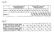
- FIG. 7A is a schematic diagram describing a first method for an image capturing device according to an exemplary embodiment of the present invention in which images captured during an ON period of a THz light source, images captured during an OFF period thereof, and the differences between their images are stored;
- FIG. 7B is a schematic diagram describing a second method for an image capturing device according to an exemplary embodiment of the present invention in which images captured during an ON period of a THz light source, images captured during an OFF period thereof, and the differences between their images are stored;
- FIG. 7C is a schematic diagram describing a third method for an image capturing device according to an exemplary embodiment of the present invention in which images captured during an ON period of a THz light source, images captured during an OFF period thereof, and the differences between their images are stored;
- FIG. 7D is a schematic diagram describing a fourth method for an image capturing device according to an exemplary embodiment of the present invention in which images captured during an ON period of a THz light source, images captured during an OFF period thereof, and the differences between their images are stored;
- FIG. 7E is a schematic diagram describing a fifth method for an image capturing device according to an exemplary embodiment of the present invention in which images captured during an ON period of a THz light source, images captured during an OFF period thereof, and the differences between their images are stored;
- FIG. 7F is a schematic diagram describing a method for an image capturing device according to an exemplary embodiment of the present invention in which images captured during an ON period of a THz light source and images captured during an OFF period thereof are stored;
- FIG. 8 is a schematic diagram describing a sample used for an image capturing device according to an exemplary embodiment of the present invention.
- FIG. 9 is a schematic diagram showing a difference in an image in which an integrated image of a plurality of images of the sample shown in FIG. 8 captured during an OFF period of a THz light source is subtracted from an integrated image of a plurality of images of the sample shown in FIG. 8 captured during an ON period thereof for an image capturing device according to an exemplary embodiment of the present invention.
- FIG. 10 is a schematic diagram showing a difference between images in which one image captured from the sample shown in FIG. 8 during an OFF period of a THz light source is subtracted from one image captured from the sample shown in FIG. 8 during an ON period thereof for the image capturing device according to the related art.
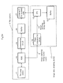
- FIG. 4 shows a structure of an image capturing device according to an exemplary embodiment of the present invention.
- the image capturing device has THz light source 1 , THz camera 4 , 1/n frequency multiplying circuit 6 , high voltage pulse power supply 8 , AND circuit 10 , drive circuit 12 , and image data obtaining device 13 .
- Image data obtaining device 13 has CPU 14 , buffer 15 , and phase compensation circuit 16 .
- CPU 14 is an example of a control unit; high voltage pulse power supply 8 is an example of a first pulse circuit; and 1/n frequency multiplying circuit 6 is an example of a second pulse circuit.
- THz wave 2 emitted by THz light source 1 is radiated to sample (measurement subject) 3 and then detected as a reflected wave or transmitted wave and captured as an image by THz camera 4 .
- sample (measurement subject) 3 it is assumed that THz wave 2 is detected as a reflected wave.
- Sync signal (image capturing timing signal) 5 that represents an image capturing timing of THz camera 4 is input from THz camera 4 to 1/n frequency multiplying circuit 6 .
- 1/n frequency multiplying circuit 6 multiplies the frequency of sync signal 5 by 1/n and thereby generates pulse sequence 7 (second pulse sequence).
- Pulse sequence 7 is input to AND circuit 10 along with pulse sequence 9 (first pulse sequence) supplied from high voltage pulse power supply 8 .
- AND circuit 10 generates new pulse sequence 11 (third pulse sequence) based on pulse sequence 7 and pulse sequence 9 .
- Pulse sequence 11 is input to drive circuit 12 and then drive circuit 12 causes THz light source 1 to oscillate (drive) based on pulse sequence 11 .
- THz camera 4 causes the ON/OFF periods of THz light source 1 to synchronize with image capturing timings of THz camera 4 so as to perform lock-in image capturing for sample 3 .
- Image data of frame images captured by THz camera 4 (hereinafter frame images are simply referred to as images) are recorded to image data obtaining device 13 .
- THz light source 1 is a QCL (Quantum Cascade Laser) that radiates an emission line at a frequency of 3.1 THz.
- QCL Quadratum Cascade Laser
- Pulse sequence 9 that is supplied from high voltage pulse power supply 8 has a pulse width of 300 nsec and a repetition frequency of 1 kHz.
- Sync signal 5 that is output from THz camera 4 is a square wave at a frequency of 60 Hz.
- 1/n frequency multiplying circuit 6 multiplies the frequency of sync signal 5 by 1/n (where n is any value that can be set) and thereby generates square pulse sequence 7 at a frequency of, for example, 15 Hz, 7.5 Hz, or 3.75 Hz.
- the frequency of pulse sequence 7 is referred to as the lock-in frequency.
- Pulse sequence 7 is input to AND circuit 10 along with pulse sequence 9 . Thereafter, AND circuit 10 performs an AND operation for pulse sequence 7 and pulse sequence 9 and thereby generates pulse sequence 11 .
- Drive circuit 12 causes THz light source (QCL) 1 to oscillate based on pulse sequence 11 .
- FIG. 5 shows an example that the lock-in frequency is 3.75 Hz.
- the frequency of pulse sequence 7 is 3.75 Hz
- eight images are captured by THz camera 4 at a frame rate of 60 Hz during an ON period of 133.3 msec of THz light source (QCL) 1 and the captured image data are recorded to image data obtaining device 13 so as to perform an image process, for example, an integration process.
- the lock-in frequency is 3.75 Hz.
- phase compensation circuit 16 disposed in image data obtaining device 13
- THz camera 4 has THz array sensor 17 , read out integrated circuit (ROIC) 18 , compensation circuit 19 , buffer 20 , and external IF (interface) 21 such as a USB (Universal Serial Bus).
- ROIC read out integrated circuit
- ROIC 18 that is a member of THz array sensor 17 obtains image data captured by THz array sensor 17 in synchronization with sync signal 5 .
- image data are updated (hereinafter the image data are referred to as internal image data).
- compensation circuit 19 performs a compensation process for image data so as to alleviate influence of various disturbances such as sensitivity fluctuations of individual sensor elements of THz array sensor 17 and those caused by fluctuations of environmental temperatures.
- Compensation circuit 19 outputs compensated image data to the outside of THz camera 4 (hereinafter, this image data are referred to as external output image data).
- this image data are referred to as external output image data.
- the update timing of the external output image data differs from that of the internal image data. Since the external output image data are output to external IF 21 through buffer 20 disposed in THz camera 4 so as to prevent data from being lost, the update timing of the external output image data further deviates. For example, when the compensation process is performed using two buffers of a data update writing buffer and an external IF output read buffer, the update timing deviates for one frame along with the delay caused by the compensation process of compensation circuit 19 .
- FIG. 6B shows an example of a delay between sync signal 5 and external IF output timing signal 22 .
- external IF output timing signal 22 shown in FIG. 6B is a signal that represents the update timing of external output image data. Due to this delay, when the external output image data that are output from THz camera 4 are supplied to CPU 14 in synchronization with sync signal 5 , an image that lies between frames or image data with a delay of a frame are obtained and thereby image data obtaining device 13 cannot accurately perform the image process as a problem that arises.
- phase compensation circuit 16 compensates the difference between the phase of sync signal 5 and the phase of the external output image data. Specifically, phase compensation circuit 16 generates image obtaining timing signal 23 such that sync signal 5 delays for a predetermined time ⁇ (compensation process time of compensation circuit 19 )+(update time of buffer 20 ) ⁇ .
- CPU 14 obtains external output image data from THz camera 4 based on image obtaining timing signal 23 .
- CPU 14 disposed in image data obtaining device 13 stores image data captured during an ON period of THz light source (QCL) 1 , image data captured during an OFF period thereof, and image data representing the differences between their images to buffer 15 , will be described.
- QCL THz light source
- FIG. 7A In a first method shown in FIG. 7A , three types of buffers X, Y, and Z are prepared. Eight pieces of image data captured during an ON period of THz light source 1 are stored in eight buffer memories X 1 ⁇ X 8 that compose buffer X; eight pieces of image data captured during an OFF period thereof are stored in eight buffer memories Y 1 ⁇ Y 8 that compose buffer Y; and then image data representing the differences between their images are stored in eight buffer memories Z 1 ⁇ Z 8 that compose buffer Z.
- two types of buffers X and Y are prepared. Eight pieces of image data captured during an ON period of THz light source 1 are stored in eight buffer memories X 1 ⁇ X 8 that compose buffer X; eight pieces of image data captured during an OFF period are stored in eight buffer memories Y 1 ⁇ Y 8 that compose buffer Y; and then image data representing the differences between their images are stored in the eight buffer memories X 1 ⁇ X 8 that compose buffer X again.
- a third method shown in FIG. 7C two types of buffers are prepared. Eight pieces of image data captured during an ON period of THz light source 1 are stored in eight buffer memories X 1 ⁇ X 8 that compose buffer X; eight pieces of image data captured during an OFF period are stored in eight buffer memories Y 1 ⁇ Y 8 that compose buffer Y; and then image data representing the differences between their images are stored in eight buffer memories Y 1 ⁇ Y 8 that compose buffer Y again.
- a fourth method shown in FIG. 7D two types of buffers X and Y are prepared.
- the number of buffer memories that compose one buffer X is eight, as in the foregoing second and third methods, the number of buffer memories that compose the other buffer Y is two, unlike the foregoing second and third methods.
- a first piece of image data captured during an OFF period is stored in first buffer memory Y 1 that composes buffer Y, the difference between the first piece of image data captured during the OFF period and the first piece of image data captured during the ON period is calculated and then image data representing the difference between images is stored in first buffer memory X 1 that composes buffer X.
- a second piece of image data captured during the OFF period is stored in second buffer memory Y 2 that composes buffer Y, the difference between the second piece of image data captured during the ON period and the second piece of image data captured during the OFF period is calculated, and then image data representing the difference between images are stored in second buffer memory X 2 that composes buffer X.
- CPU 14 integrates image data representing the difference between images obtained as described above and displays integrated image data representing the difference between images.
- CPU 14 may perform a method in which image data are integrated before differences between images are obtained instead of a method in which image data are integrated after image data representing differences between images are obtained.
- CPU 14 integrates a plurality of pieces of image data captured during an ON period of THz light source (QCL) 1 , integrates a plurality of pieces of image data captured during an OFF period thereof, calculates the differences between the integrated image data of the plurality of pieces of image data captured during the ON period and the integrated image data of the plurality of pieces of image data captured during the OFF period, and then displays the difference between images of the integrated image data.
- QCL THz light source
- CPU 14 cannot simultaneously perfoim a method in which image data are integrated after image data representing the differences between images are obtained and a method in which image data are integrated before image data representing the differences between images are obtained. Thus, one of these methods needs to have been set for CPU 14 .
- two types of buffers X and Y are prepared. Eight pieces of image data captured during an ON period of THz light source 1 are stored in eight buffer memories X 1 ⁇ X 8 that compose buffer X and then eight pieces of image data captured during an OFF period thereof are stored in eight buffer memories Y 1 ⁇ Y 8 that compose buffer Y.
- sample 3 in which black cloth tape 25 is adhered on an Al tape coated on reflection plate 24 is prepared.
- An emission line at a frequency of 3.1 THz that is emitted by THz light source (QCL) 1 that is cooled by liquid nitrogen is radiated to partial region 26 of reflection plate 24 .
- a reflection image whose emission line has been reflected by reflection plate 24 is captured by THz camera 4 that is provided with THz array sensor 17 that have 320 * 240 pixels arranged at a pitch of 23.5 ⁇ m.
- FIG. 9 is a reflection image of an emission line emitted by THz light source (QCL) 1 and reflected by reflection plate 24 (the reflection image is depicted as an elongated portion nearly at the center of the figure).
- the reflection image is formed in an elongated shape because an off-axis parabolic mirror (not shown) disposed in THz light source (QCL) 1 has an aberration. Since the reflectance of black cloth tape 25 is low, low luminance portion 27 appears nearly at the center of the elongated portion. Low luminance portion 27 corresponds to position 28 of cloth tape 25 .
- FIG. 9 shows a difference in an image in which the difference between an integrated image of seven pieces of the second to the eighth piece of image data captured during an ON period of THz light source 1 and an integrated image of seven pieces of the second to the eighth piece of image data captured during an OFF period thereof is calculated at a lock-in frequency of 3.75 Hz.
- the first piece of image data is not used taking account of the fact that the time constant of THz array sensor 17 is 16 msec and thereby a signal of the first frame might have been not fully raised or lowered during the ON period or OFF period of THz light source (QCL) 1 .
- image data are stored in buffer 15 based on the method shown in FIG. 7F .
- image data of 24 * 24 pixels are integrated so as to further improve the signal-to-noise ratio.
- the signal-to-noise ratio of high luminance portion 29 on the right of a QCL image shown in FIG. 9 is around 400.
- FIG. 10 shows a difference in an image between one piece of image data captured during an ON period of THz light source (QCL) 1 and one piece of image data captured during an OFF period thereof so as to check out how the present invention improves the signal-to-noise ratio compared to the related art.
- This difference in the image corresponds to an image obtained based on a function of the image capturing device according to the related art.
- Sample 3 is the same as the sample from which the image shown in FIG. 9 is captured.
- the shape of the image shown in FIG. 10 is the same as that shown in FIG. 9 .
- the lock-in frequency at which the differences between image shown in FIG. 10 is obtained is also 3.75 Hz.
- the signal-to-noise ratio of high luminance portion 29 on the right of a QCL image shown in FIG. 10 is around 135.
- the present invention (shown in FIG. 9 ) can improve the signal-to-noise ratio two to three times compared to the related art (shown in FIG. 10 ).
- successive seven pieces from among all eight pieces of image data captured during ON/OFF periods of THz light source 1 were used.
- all eight pieces of image data may be used.
- seven pieces from the first to the seventh piece of image data may be used.
- a plurality of successive pieces from among all pieces of image data captured during the ON/OFF periods of THz light source 1 may be selected and used.
- a reflection image reflected by sample 3 was obtained.
- a transmission image that transmits through sample 3 may be obtained.
- the foregoing exemplary embodiments deal with electromagnetic waves of a THz frequency band.
- the present invention can be applied to electromagnetic waves of other frequency bands as well as such a frequency band.
- An image capturing device having a light source and a camera that captures an image of a measurement subject placed in an optical path that lies between said camera itself and said light source, comprising:
- control unit that subtracts a plurality of frame images captured by said camera during an OFF period of said light source from a plurality of frame images captured by said camera during an ON period of said light source, the number of frame images captured by said camera during the OFF period being the same as that number of frame images obtained by said camera during the ON period and integrates the differences between their images.
- control unit stores a plurality of frame images captured by said camera during the ON period of said light source in a first buffer
- control unit stores a plurality of frame images captured by said camera during the OFF period of said light source in a second buffer
- control unit subtracts the plurality of frame images stored in said second buffer from the plurality of frame images stored in said first buffer and stores the differences between their images in a third buffer, the number of frame images stored in said second buffer being the same as the number of frame images stored in said first buffer, and
- control unit integrates the differences between images stored in said third buffer.
- control unit selects any successive frame images from among all the frame images captured by said camera during the ON period of said light source
- control unit selects successive frame images from among all frame images captured by said camera during the OFF period of said light source, the successful number of frame images selected from among all frame images captured during the ON period being the same as the successive number of frame images selected from among all frame images captured during the OFF period.
- the image capturing device as set forth in supplementary note 2 or 3,
- control unit uses said first buffer or said second buffer as said third buffer.
- control unit stores a plurality of frame images captured by said camera during the ON period of said light source and a plurality of frame images captured by said camera during the OFF period of said light source in a first buffer, the number of frame images captured by said camera during the ON period of said light source being the same as the number of frame images captured by said camera during the OFF period of said light source,
- control unit subtracts the plurality of frame images captured by said camera during the OFF period of said light source and stored in said first buffer from the plurality of frame images captured by said camera during the ON period of said light source and stored in said first buffer and stores the differences between their images in said second buffer, the number of frame images captured by said camera during the OFF period of said light source and stored in said second buffer being the same as the number of frame images captured by said camera during the ON period of said light source and stored in said first buffer, and
- control unit integrates the differences between images stored in said second buffer.
- An image capturing device having a light source and a camera that captures an image of a measurement subject placed in an optical path that lies between said camera itself and said light source, comprising:
- a control unit that integrates a plurality of frame images captured by said camera during an ON period of said light source, integrates a plurality of frame images captured by said camera during an OFF period of said light source, the number of frame images captured by said camera during the ON period being the same as the number of frame images captured by said camera during the OFF period, subtracts an integrated image of the frame images captured by said camera during the OFF period of said light source from an integrated image of the frame images captured by said camera during the ON period of said light source, and obtains the difference between their images.
- control unit selects any successive frame images from among all the frame images captured by said camera during the ON period of said light source and integrates the selected frame images
- control unit selects successive frame images from among all the frame images captured by said camera during the OFF period of said light source, the number of frame images captured by said camera during the OFF period being the same as the number of frame images captured by said camera during the ON period, and integrates the selected frame images.
- the image capturing device as set forth in any one of supplementary notes 1 to 7, further comprising:
- a second pulse circuit that generates a second pulse sequence based on an image capturing timing signal that represents an image capturing timing of said camera, said second pulse sequence having a lower frequency than does the image capturing timing signal;
- a drive circuit that drives said light source based on a third pulse sequence that is a calculation result of the AND operation of said AND circuit.
- said second pulse circuit is capable of setting any frequency that is lower than the frequency of said image capturing timing signal and generates said second pulse sequence at the frequency that has been set.
- the image capturing device as set forth in supplementary note 8 or 9, further comprising:
- phase compensation circuit that generates an image obtaining signal of which said image capturing timing signal is delayed for a predeteimined time
- control unit obtains frame images captured by said camera based on said image obtaining signal.
- An image capturing method for an image capturing device having a light source and a camera that captures an image of a measurement subject placed in an optical path that lies between said camera itself and said light source comprising:
- An image capturing method for an image capturing device having a light source and a camera that captures an image of a measurement subject placed in an optical path that lies between said camera itself and said light source comprising:
Landscapes
- Physics & Mathematics (AREA)
- General Physics & Mathematics (AREA)
- Spectroscopy & Molecular Physics (AREA)
- Health & Medical Sciences (AREA)
- Toxicology (AREA)
- Life Sciences & Earth Sciences (AREA)
- Chemical & Material Sciences (AREA)
- Analytical Chemistry (AREA)
- Biochemistry (AREA)
- General Health & Medical Sciences (AREA)
- Immunology (AREA)
- Pathology (AREA)
- Studio Devices (AREA)
- Stroboscope Apparatuses (AREA)
- Investigating Or Analysing Materials By Optical Means (AREA)
- Length Measuring Devices By Optical Means (AREA)
Abstract
Description
- This application is based upon and claims the benefit of priority from Japanese patent application No. 2011-070058, filed on Mar. 28, 2011, the disclosure of which is incorporated herein in its entirety by reference.
- 1. Field of the Invention
- The present invention relates to an image capturing device that is provided with a light source and a camera and in which a measurement subject is placed in an optical path that lies therebetween, in particular, to an image capturing device that captures an image of a measurement subject in synchronization with ON/OFF states of the light source.
- 2. Description of the Related Art
- Image capturing devices that are provided with a light source and a camera and in which a measurement subject is placed in an optical path that lies therebetween are known. In these image capturing devices, when an image of a measurement subject is captured in synchronization with the ON/OFF states of the light source (so-called lock-in image capturing), not only images caused by radiations other than the light source can be eliminated, but also low-frequency noises such as 1/f noises can be set to the off setting.
- For example, as presented in Non-patent Literature 1 (A. W. M. Lee et al., IEEE PHOTONICS TECHNOLOGY LETTERS,
VOL 18, NO. 13, Jul. 1, 2006, p. 1415-1417), when a THz wave emitted by a THz light source that is periodically turned ON and OFF is transmitted to a camera whose sensitivity is within a range from the infrared region to the THz (terahertz) region, the camera detects an electromagnetic wave in which infrared and a periodic THz wave have been mixed and captures an image based on the detected electromagnetic wave. By calculating the difference between image data captured by the camera during the ON period of the THz light source and image data captured by the camera during the OFF period thereof, infrared images can be set off and thereby only THz images can be obtained. As a result, a filter that suppresses infrared waves and passes through only THz waves can be omitted. - A specific arrangement of the foregoing image capturing device is shown in
FIG. 1 . - As shown in
FIG. 1 , light of a THz wave at a frequency of 4.3 THz (with a wavelength of 70 μm) is emitted by QCL (Quantum Cascade Laser) 102 that is mounted on cooler 101. The light travels to off-axisparabolic mirror 103. Off-axis parabolic minor 103 collimates the light and reflects the collimated light to off-axisparabolic mirror 104. Off-axisparabolic mirror 104 radiates the collimated light to envelop (measurement subject) 105. The light that has passed throughenvelop 105 is collected bySi lens 106 tomicrobolometer array sensor 108 that has 320×240 pixels and that is mounted on microbolometer camera 107 (at a frame rate of 60 Hz).Microbolometer array sensor 108 captures an image based on the collected light of the THz wave. -
FIG. 2 shows a lock-in image capturing method for the image capturing device shown inFIG. 1 . - As shown in
FIG. 2 ,QCL 102 is turned ON atframe 1 andQCL 102 is turned OFF atframe 2 andframe 3. - At
frame 1, an infrared wave and THz wave emitted byQCL 102 are collected tomicrobolometer array sensor 108 and thereby an image is captured based on both the infrared and THz wave, whereas atframe 2 andframe 3, only infrared waves are collected tomicrobolometer array sensor 108 and thereby an image is captured based on only the infrared. - Thus, by calculating the difference between the image data of
frame 1 and the image data offrame 3, a THz image can be obtained as an image captured based on only the THz wave emitted byQCL 102. -
Frame 2 is not used in order to increase the difference between image data offrame 1 and image data offrame 3 since a sufficiently long time elapses after the image data offrame 1 has been captured compared to a thermal time constant of around 13 msec ofmicrobolometer array sensor 108. -
FIG. 3 showsTHz image 110 that is captured fromenvelop 105 that containspaper 109 with letters “MIT” written with a pencil at a frame rate of 20 Hz based on the method shown inFIG. 2 . Thus, letters “MIT” can be checked out without necessity ofopening envelop 105. - However, in the foregoing image capturing device, since only the difference between one piece of image data captured during the ON period of the light source and one piece of image data captured during the OFF period thereof, as a problem that would arise, the signal-to-noise ratio could not be improved as expected.
- Therefore, an object of the present invention is to provide an image capturing device and an image capturing method that can solve the foregoing problem.
- A first image capturing device according to the present invention is an image capturing device having a light source and a camera that captures an image of a measurement subject placed in an optical path that lies between said camera itself and said light source, comprising:
- a control unit that subtracts a plurality of frame images captured by said camera during an OFF period of said light source from a plurality of frame images captured by said camera during an ON period of said light source, the number of frame images captured by said camera during the OFF period being the same as that number of frame images obtained by said camera during the ON period and integrates the differences between their images.
- A second image capturing device according to the present invention is an image capturing device having a light source and a camera that captures an image of a measurement subject placed in an optical path that lies between said camera itself and said light source, comprising:
- a control unit that integrates a plurality of frame images captured by said camera during an ON period of said light source, integrates a plurality of frame images captured by said camera during an OFF period of said light source, the number of frame images captured by said camera during the ON period being the same as the number of frame images captured by said camera during the OFF period, subtracts an integrated image of the frame images captured by said camera during the OFF period of said light source from an integrated image of the frame images captured by said camera during the ON period of said light source, and obtains the difference between their images.
- A first image capturing method according to the present invention is an image capturing method for an image capturing device having a light source and a camera that captures an image of a measurement subject placed in an optical path that lies between said camera itself and said light source, comprising:
- subtracting a plurality of frame images captured by said camera during an OFF period of said light source from a plurality of frame images captured by said camera during an ON period of said light source, the number of frame images captured by said camera during the OFF period being the same as the number of frame images captured by said camera during the ON period, and integrating the differences between their images.
- A second image capturing method according to the present invention is an image capturing method for an image capturing device having a light source and a camera that captures an image of a measurement subject placed in an optical path that lies between said camera itself and said light source, comprising:
- integrating a plurality of frame images captured by said camera during an ON period of said light source;
- integrating a plurality of frame images captured by said camera during an OFF period of said light source, the number of frame images captured by said camera during the OFF period being the same as the number of frame images captured by said camera during the ON period; and
- subtracting an integrated image of the frame images captured by said camera during the OFF period of said light source from an integrated image of the frame images captured by said camera during the ON period of said light source and obtaining the difference between their images.
- According to the first image capturing device and the first image capturing method of the present invention, a plurality of frame images captured during an OFF period of a light source are subtracted from a plurality of frame images captured during an ON period thereof, the number of frame images captured during the ON period being the same as the number of frame images captured during the OFF period, and then the differences between their images are integrated.
- According to a second image capturing device and a second image capturing method of the present invention, an integrated image of a plurality of frame images captured during an OFF period of a light source is subtracted from an integrated image of a plurality of frame images captured during an ON period thereof, the number of frame images captured during the OFF period being the same as the number of frame images captured during the ON period, and the difference between the images is obtained.
- Thus, as an effect of the present invention, the signal-to-noise ratio can be improved compared to the related art in which the difference between one image captured during an ON period of a light source and one image captured during an OFF period thereof is calculated and the difference between the images is obtained.
- The above and other objects, features, and advantages of the present invention will become apparent from the following description with reference to the accompanying drawings which illustrate examples of the present invention.
-
FIG. 1 is a schematic diagram showing a structure of an image capturing device according to a related art; -
FIG. 2 is a schematic diagram describing a method to obtain the difference between their images for the image capturing device according to the related art; -
FIG. 3 is a schematic diagram showing a THz transmission image captured by the image capturing device according to the related art; -
FIG. 4 is a schematic diagram showing a structure of an image capturing device according to an exemplary embodiment of the present invention; -
FIG. 5 is a schematic diagram describing a pulse sequence used in the image capturing device according to the exemplary embodiment of the present invention; -
FIG. 6A is a schematic diagram describing a function that compensates phases of image data for the image capturing device according to the exemplary embodiment of the present invention; -
FIG. 6B is a schematic diagram describing the relationship among an image capturing timing signal, an external IF output timing signal, and an image obtaining timing signal for the image capturing device according to the exemplary embodiments of the present invention; -
FIG. 7A is a schematic diagram describing a first method for an image capturing device according to an exemplary embodiment of the present invention in which images captured during an ON period of a THz light source, images captured during an OFF period thereof, and the differences between their images are stored; -
FIG. 7B is a schematic diagram describing a second method for an image capturing device according to an exemplary embodiment of the present invention in which images captured during an ON period of a THz light source, images captured during an OFF period thereof, and the differences between their images are stored; -
FIG. 7C is a schematic diagram describing a third method for an image capturing device according to an exemplary embodiment of the present invention in which images captured during an ON period of a THz light source, images captured during an OFF period thereof, and the differences between their images are stored; -
FIG. 7D is a schematic diagram describing a fourth method for an image capturing device according to an exemplary embodiment of the present invention in which images captured during an ON period of a THz light source, images captured during an OFF period thereof, and the differences between their images are stored; -
FIG. 7E is a schematic diagram describing a fifth method for an image capturing device according to an exemplary embodiment of the present invention in which images captured during an ON period of a THz light source, images captured during an OFF period thereof, and the differences between their images are stored; -
FIG. 7F is a schematic diagram describing a method for an image capturing device according to an exemplary embodiment of the present invention in which images captured during an ON period of a THz light source and images captured during an OFF period thereof are stored; -
FIG. 8 is a schematic diagram describing a sample used for an image capturing device according to an exemplary embodiment of the present invention; -
FIG. 9 is a schematic diagram showing a difference in an image in which an integrated image of a plurality of images of the sample shown inFIG. 8 captured during an OFF period of a THz light source is subtracted from an integrated image of a plurality of images of the sample shown inFIG. 8 captured during an ON period thereof for an image capturing device according to an exemplary embodiment of the present invention; and -
FIG. 10 is a schematic diagram showing a difference between images in which one image captured from the sample shown inFIG. 8 during an OFF period of a THz light source is subtracted from one image captured from the sample shown inFIG. 8 during an ON period thereof for the image capturing device according to the related art. - Next, with reference to the accompanying drawings, exemplary embodiments of the present invention will be described.
-
FIG. 4 shows a structure of an image capturing device according to an exemplary embodiment of the present invention. - As shown in
FIG. 4 , the image capturing device according to this exemplary embodiment has THzlight source 1,THz camera frequency multiplying circuit 6, high voltagepulse power supply 8, ANDcircuit 10,drive circuit 12, and imagedata obtaining device 13. Imagedata obtaining device 13 hasCPU 14,buffer 15, andphase compensation circuit 16. - In
FIG. 4 ,CPU 14 is an example of a control unit; high voltagepulse power supply 8 is an example of a first pulse circuit; and 1/nfrequency multiplying circuit 6 is an example of a second pulse circuit. -
THz wave 2 emitted by THzlight source 1 is radiated to sample (measurement subject) 3 and then detected as a reflected wave or transmitted wave and captured as an image byTHz camera 4. According to this exemplary embodiment, it is assumed thatTHz wave 2 is detected as a reflected wave. - Sync signal (image capturing timing signal) 5 that represents an image capturing timing of
THz camera 4 is input fromTHz camera 4 to 1/nfrequency multiplying circuit 6. 1/nfrequency multiplying circuit 6 multiplies the frequency ofsync signal 5 by 1/n and thereby generates pulse sequence 7 (second pulse sequence). -
Pulse sequence 7 is input to ANDcircuit 10 along with pulse sequence 9 (first pulse sequence) supplied from high voltagepulse power supply 8. ANDcircuit 10 generates new pulse sequence 11 (third pulse sequence) based onpulse sequence 7 andpulse sequence 9. -
Pulse sequence 11 is input to drivecircuit 12 and then drivecircuit 12 causes THzlight source 1 to oscillate (drive) based onpulse sequence 11. -
THz camera 4 causes the ON/OFF periods of THzlight source 1 to synchronize with image capturing timings ofTHz camera 4 so as to perform lock-in image capturing forsample 3. Image data of frame images captured by THz camera 4 (hereinafter frame images are simply referred to as images) are recorded to imagedata obtaining device 13. - Here, a specific working example of the image capturing device according to this exemplary embodiment will be described.
- THz
light source 1 is a QCL (Quantum Cascade Laser) that radiates an emission line at a frequency of 3.1 THz. -
Pulse sequence 9 that is supplied from high voltagepulse power supply 8 has a pulse width of 300 nsec and a repetition frequency of 1 kHz. -
Sync signal 5 that is output fromTHz camera 4 is a square wave at a frequency of 60 Hz. - 1/n
frequency multiplying circuit 6 multiplies the frequency ofsync signal 5 by 1/n (where n is any value that can be set) and thereby generatessquare pulse sequence 7 at a frequency of, for example, 15 Hz, 7.5 Hz, or 3.75 Hz. The frequency ofpulse sequence 7 is referred to as the lock-in frequency. -
Pulse sequence 7 is input to ANDcircuit 10 along withpulse sequence 9. Thereafter, ANDcircuit 10 performs an AND operation forpulse sequence 7 andpulse sequence 9 and thereby generatespulse sequence 11. Drivecircuit 12 causes THz light source (QCL) 1 to oscillate based onpulse sequence 11.FIG. 5 shows an example that the lock-in frequency is 3.75 Hz. - As shown in
FIG. 5 , when the frequency ofpulse sequence 7 is 3.75 Hz, eight images are captured byTHz camera 4 at a frame rate of 60 Hz during an ON period of 133.3 msec of THz light source (QCL) 1 and the captured image data are recorded to imagedata obtaining device 13 so as to perform an image process, for example, an integration process. In the following, it is assumed that the lock-in frequency is 3.75 Hz. - Here, with reference to
FIG. 6A andFIG. 6B , functions ofphase compensation circuit 16 disposed in imagedata obtaining device 13 will be described. - As shown in
FIG. 6A ,THz camera 4 hasTHz array sensor 17, read out integrated circuit (ROIC) 18,compensation circuit 19,buffer 20, and external IF (interface) 21 such as a USB (Universal Serial Bus). - In
THz camera 4,ROIC 18 that is a member ofTHz array sensor 17 obtains image data captured byTHz array sensor 17 in synchronization withsync signal 5. As a result, image data are updated (hereinafter the image data are referred to as internal image data). - Moreover, in
THz camera 4,compensation circuit 19 performs a compensation process for image data so as to alleviate influence of various disturbances such as sensitivity fluctuations of individual sensor elements ofTHz array sensor 17 and those caused by fluctuations of environmental temperatures. -
Compensation circuit 19 outputs compensated image data to the outside of THz camera 4 (hereinafter, this image data are referred to as external output image data). Thus, the update timing of the external output image data differs from that of the internal image data. Since the external output image data are output to external IF 21 throughbuffer 20 disposed inTHz camera 4 so as to prevent data from being lost, the update timing of the external output image data further deviates. For example, when the compensation process is performed using two buffers of a data update writing buffer and an external IF output read buffer, the update timing deviates for one frame along with the delay caused by the compensation process ofcompensation circuit 19. -
FIG. 6B shows an example of a delay betweensync signal 5 and external IFoutput timing signal 22. Here, external IFoutput timing signal 22 shown inFIG. 6B is a signal that represents the update timing of external output image data. Due to this delay, when the external output image data that are output fromTHz camera 4 are supplied toCPU 14 in synchronization withsync signal 5, an image that lies between frames or image data with a delay of a frame are obtained and thereby imagedata obtaining device 13 cannot accurately perform the image process as a problem that arises. - To solve this problem, according to this exemplary embodiment,
phase compensation circuit 16 compensates the difference between the phase ofsync signal 5 and the phase of the external output image data. Specifically,phase compensation circuit 16 generates image obtainingtiming signal 23 such thatsync signal 5 delays for a predetermined time {(compensation process time of compensation circuit 19)+(update time of buffer 20)}.CPU 14 obtains external output image data fromTHz camera 4 based on image obtainingtiming signal 23. - Next, with reference to
FIG. 7A toFIG. 7E , examples of methods in whichCPU 14 disposed in imagedata obtaining device 13 stores image data captured during an ON period of THz light source (QCL) 1, image data captured during an OFF period thereof, and image data representing the differences between their images to buffer 15, will be described. - In a first method shown in
FIG. 7A , three types of buffers X, Y, and Z are prepared. Eight pieces of image data captured during an ON period of THzlight source 1 are stored in eight buffer memories X1˜X8 that compose buffer X; eight pieces of image data captured during an OFF period thereof are stored in eight buffer memories Y1˜Y8 that compose buffer Y; and then image data representing the differences between their images are stored in eight buffer memories Z1˜Z8 that compose buffer Z. - In a second method shown in
FIG. 7B , two types of buffers X and Y are prepared. Eight pieces of image data captured during an ON period of THzlight source 1 are stored in eight buffer memories X1˜X8 that compose buffer X; eight pieces of image data captured during an OFF period are stored in eight buffer memories Y1˜Y8 that compose buffer Y; and then image data representing the differences between their images are stored in the eight buffer memories X1˜X8 that compose buffer X again. - In a third method shown in
FIG. 7C , two types of buffers are prepared. Eight pieces of image data captured during an ON period of THzlight source 1 are stored in eight buffer memories X1˜X8 that compose buffer X; eight pieces of image data captured during an OFF period are stored in eight buffer memories Y1˜Y8 that compose buffer Y; and then image data representing the differences between their images are stored in eight buffer memories Y1˜Y8 that compose buffer Y again. - In a fourth method shown in
FIG. 7D , two types of buffers X and Y are prepared. However, although the number of buffer memories that compose one buffer X is eight, as in the foregoing second and third methods, the number of buffer memories that compose the other buffer Y is two, unlike the foregoing second and third methods. In other words, eight pieces of image data captured during an ON period of THzlight source 1 are stored in eight buffer memories Xi (where i=1, 2, . . . , 8) that compose buffer X. Thereafter, a first piece of image data captured during an OFF period is stored in first buffer memory Y1 that composes buffer Y, the difference between the first piece of image data captured during the OFF period and the first piece of image data captured during the ON period is calculated and then image data representing the difference between images is stored in first buffer memory X1 that composes buffer X. While the calculation and storing procedures are being performed, a second piece of image data captured during the OFF period is stored in second buffer memory Y2 that composes buffer Y, the difference between the second piece of image data captured during the ON period and the second piece of image data captured during the OFF period is calculated, and then image data representing the difference between images are stored in second buffer memory X2 that composes buffer X. This calculation and storing procedures are performed alternately using two buffer memories Y1 and Y2 that compose buffer Y. As a result, calculation results of X2n+1−Y1 (where n=0, 1, 2, 3) are stored in X2n+1, whereas the calculation results of X2n−Y2 (where n=1, 2, 3, 4) are stored in X2n. - In a fifth method shown in
FIG. 7E , eight pieces of image data captured during an ON period of THzlight source 1 and eight pieces of image data captured during an OFF period thereof are stored inbuffer 1 and image data representing the differences between their images are stored inbuffer 2. -
CPU 14 integrates image data representing the difference between images obtained as described above and displays integrated image data representing the difference between images. - Alternatively,
CPU 14 may perform a method in which image data are integrated before differences between images are obtained instead of a method in which image data are integrated after image data representing differences between images are obtained. - In other words,
CPU 14 integrates a plurality of pieces of image data captured during an ON period of THz light source (QCL) 1, integrates a plurality of pieces of image data captured during an OFF period thereof, calculates the differences between the integrated image data of the plurality of pieces of image data captured during the ON period and the integrated image data of the plurality of pieces of image data captured during the OFF period, and then displays the difference between images of the integrated image data. - With reference to
FIG. 7F , such an example in which image data captured during an ON period of THz light source (QCL) 1 and image data captured during an OFF period thereof are stored inbuffer 15 disposed in imagedata obtaining device 13 will be described. - However,
CPU 14 cannot simultaneously perfoim a method in which image data are integrated after image data representing the differences between images are obtained and a method in which image data are integrated before image data representing the differences between images are obtained. Thus, one of these methods needs to have been set forCPU 14. - In the method shown in
FIG. 7F , two types of buffers X and Y are prepared. Eight pieces of image data captured during an ON period of THzlight source 1 are stored in eight buffer memories X1˜X8 that compose buffer X and then eight pieces of image data captured during an OFF period thereof are stored in eight buffer memories Y1˜Y8 that compose buffer Y. - Next, with reference to
FIG. 8 ,FIG. 9 , andFIG. 10 , an example in which integrated image data representing the differences between images are calculated in the foregoing manner and thereby the signal-to-noise is improved two to three times compared to the related art will be described. In the following, it is assumed that image data are integrated before image data representing the differences between images are obtained. - As shown in
FIG. 8 ,sample 3 in whichblack cloth tape 25 is adhered on an Al tape coated onreflection plate 24 is prepared. An emission line at a frequency of 3.1 THz that is emitted by THz light source (QCL) 1 that is cooled by liquid nitrogen is radiated topartial region 26 ofreflection plate 24. A reflection image whose emission line has been reflected byreflection plate 24 is captured byTHz camera 4 that is provided withTHz array sensor 17 that have 320 * 240 pixels arranged at a pitch of 23.5 μm. -
FIG. 9 is a reflection image of an emission line emitted by THz light source (QCL) 1 and reflected by reflection plate 24 (the reflection image is depicted as an elongated portion nearly at the center of the figure). The reflection image is formed in an elongated shape because an off-axis parabolic mirror (not shown) disposed in THz light source (QCL) 1 has an aberration. Since the reflectance ofblack cloth tape 25 is low,low luminance portion 27 appears nearly at the center of the elongated portion.Low luminance portion 27 corresponds to position 28 ofcloth tape 25. -
FIG. 9 shows a difference in an image in which the difference between an integrated image of seven pieces of the second to the eighth piece of image data captured during an ON period of THzlight source 1 and an integrated image of seven pieces of the second to the eighth piece of image data captured during an OFF period thereof is calculated at a lock-in frequency of 3.75 Hz. The first piece of image data is not used taking account of the fact that the time constant ofTHz array sensor 17 is 16 msec and thereby a signal of the first frame might have been not fully raised or lowered during the ON period or OFF period of THz light source (QCL) 1. In this case, image data are stored inbuffer 15 based on the method shown inFIG. 7F . In addition, image data of 24 * 24 pixels are integrated so as to further improve the signal-to-noise ratio. The signal-to-noise ratio ofhigh luminance portion 29 on the right of a QCL image shown inFIG. 9 is around 400. -
FIG. 10 shows a difference in an image between one piece of image data captured during an ON period of THz light source (QCL) 1 and one piece of image data captured during an OFF period thereof so as to check out how the present invention improves the signal-to-noise ratio compared to the related art. This difference in the image corresponds to an image obtained based on a function of the image capturing device according to the related art.Sample 3 is the same as the sample from which the image shown inFIG. 9 is captured. The shape of the image shown inFIG. 10 is the same as that shown inFIG. 9 . The lock-in frequency at which the differences between image shown inFIG. 10 is obtained is also 3.75 Hz. The signal-to-noise ratio ofhigh luminance portion 29 on the right of a QCL image shown inFIG. 10 is around 135. - Thus, it is clear that the present invention (shown in
FIG. 9 ) can improve the signal-to-noise ratio two to three times compared to the related art (shown inFIG. 10 ). - With reference to the exemplary embodiments, the present invention has been described. However, it should be understood by those skilled in the art that the structure and details of the present invention may be changed in various manners without departing from the scope of the present invention.
- According to foregoing exemplary embodiments, successive seven pieces from among all eight pieces of image data captured during ON/OFF periods of THz
light source 1 were used. Alternatively, as long as the time constant ofTHz array sensor 17 is low, all eight pieces of image data may be used. Alternatively, seven pieces from the first to the seventh piece of image data may be used. In other words, according to the present invention, a plurality of successive pieces from among all pieces of image data captured during the ON/OFF periods of THzlight source 1 may be selected and used. - In addition, according to a foregoing exemplary embodiment, a reflection image reflected by
sample 3 was obtained. Alternatively, a transmission image that transmits throughsample 3 may be obtained. - In addition, the foregoing exemplary embodiments deal with electromagnetic waves of a THz frequency band. Alternatively, the present invention can be applied to electromagnetic waves of other frequency bands as well as such a frequency band.
- The whole or part of the exemplary embodiments disclosed above can be described as but not limited to, the following supplementary notes.
- An image capturing device having a light source and a camera that captures an image of a measurement subject placed in an optical path that lies between said camera itself and said light source, comprising:
- a control unit that subtracts a plurality of frame images captured by said camera during an OFF period of said light source from a plurality of frame images captured by said camera during an ON period of said light source, the number of frame images captured by said camera during the OFF period being the same as that number of frame images obtained by said camera during the ON period and integrates the differences between their images.
- The image capturing device as set forth in
supplementary note 1, - wherein said control unit stores a plurality of frame images captured by said camera during the ON period of said light source in a first buffer,
- wherein said control unit stores a plurality of frame images captured by said camera during the OFF period of said light source in a second buffer,
- wherein said control unit subtracts the plurality of frame images stored in said second buffer from the plurality of frame images stored in said first buffer and stores the differences between their images in a third buffer, the number of frame images stored in said second buffer being the same as the number of frame images stored in said first buffer, and
- wherein said control unit integrates the differences between images stored in said third buffer.
- The image capturing device as set forth in
supplementary note 2, - wherein said control unit selects any successive frame images from among all the frame images captured by said camera during the ON period of said light source, and
- wherein said control unit selects successive frame images from among all frame images captured by said camera during the OFF period of said light source, the successful number of frame images selected from among all frame images captured during the ON period being the same as the successive number of frame images selected from among all frame images captured during the OFF period.
- The image capturing device as set forth in
supplementary note - wherein said control unit uses said first buffer or said second buffer as said third buffer.
- The image capturing device as set forth in
supplementary note 1, - wherein said control unit stores a plurality of frame images captured by said camera during the ON period of said light source and a plurality of frame images captured by said camera during the OFF period of said light source in a first buffer, the number of frame images captured by said camera during the ON period of said light source being the same as the number of frame images captured by said camera during the OFF period of said light source,
- wherein said control unit subtracts the plurality of frame images captured by said camera during the OFF period of said light source and stored in said first buffer from the plurality of frame images captured by said camera during the ON period of said light source and stored in said first buffer and stores the differences between their images in said second buffer, the number of frame images captured by said camera during the OFF period of said light source and stored in said second buffer being the same as the number of frame images captured by said camera during the ON period of said light source and stored in said first buffer, and
- wherein said control unit integrates the differences between images stored in said second buffer.
- An image capturing device having a light source and a camera that captures an image of a measurement subject placed in an optical path that lies between said camera itself and said light source, comprising:
- a control unit that integrates a plurality of frame images captured by said camera during an ON period of said light source, integrates a plurality of frame images captured by said camera during an OFF period of said light source, the number of frame images captured by said camera during the ON period being the same as the number of frame images captured by said camera during the OFF period, subtracts an integrated image of the frame images captured by said camera during the OFF period of said light source from an integrated image of the frame images captured by said camera during the ON period of said light source, and obtains the difference between their images.
- The image capturing device as set forth in
supplementary note 6, - wherein said control unit selects any successive frame images from among all the frame images captured by said camera during the ON period of said light source and integrates the selected frame images, and
- wherein said control unit selects successive frame images from among all the frame images captured by said camera during the OFF period of said light source, the number of frame images captured by said camera during the OFF period being the same as the number of frame images captured by said camera during the ON period, and integrates the selected frame images.
- The image capturing device as set forth in any one of
supplementary notes 1 to 7, further comprising: - a first pulse circuit that generates a first pulse sequence;
- a second pulse circuit that generates a second pulse sequence based on an image capturing timing signal that represents an image capturing timing of said camera, said second pulse sequence having a lower frequency than does the image capturing timing signal;
- an AND circuit that perfonns an AND operation for said first pulse sequence and said second pulse sequence; and
- a drive circuit that drives said light source based on a third pulse sequence that is a calculation result of the AND operation of said AND circuit.
- The image capturing device as set forth in
supplementary note 8, - wherein said second pulse circuit is capable of setting any frequency that is lower than the frequency of said image capturing timing signal and generates said second pulse sequence at the frequency that has been set.
- The image capturing device as set forth in
supplementary note - a phase compensation circuit that generates an image obtaining signal of which said image capturing timing signal is delayed for a predeteimined time,
- wherein said control unit obtains frame images captured by said camera based on said image obtaining signal.
- An image capturing method for an image capturing device having a light source and a camera that captures an image of a measurement subject placed in an optical path that lies between said camera itself and said light source, comprising:
- subtracting a plurality of frame images captured by said camera during an OFF period of said light source from a plurality of frame images captured by said camera during an ON period of said light source, the number of frame images captured by said camera during the OFF period being the same as the number of frame images captured by said camera during the ON period, and integrating the differences between their images.
- An image capturing method for an image capturing device having a light source and a camera that captures an image of a measurement subject placed in an optical path that lies between said camera itself and said light source, comprising:
- integrating a plurality of frame images captured by said camera during an ON period of said light source;
- integrating a plurality of frame images captured by said camera during an OFF period of said light source, the number of frame images captured by said camera during the OFF period being the same as the number of frame images captured by said camera during the ON period; and
- subtracting an integrated image of the frame images captured by said camera during the OFF period of said light source from an integrated image of the frame images captured by said camera during the ON period of said light source and obtaining the differences between their images.
Claims (11)
Applications Claiming Priority (2)
| Application Number | Priority Date | Filing Date | Title |
|---|---|---|---|
| JP2011070058A JP5305482B2 (en) | 2011-03-28 | 2011-03-28 | Imaging apparatus and imaging method |
| JP2011-070058 | 2011-03-28 |
Publications (2)
| Publication Number | Publication Date |
|---|---|
| US20120249782A1 true US20120249782A1 (en) | 2012-10-04 |
| US9164030B2 US9164030B2 (en) | 2015-10-20 |
Family
ID=46087193
Family Applications (1)
| Application Number | Title | Priority Date | Filing Date |
|---|---|---|---|
| US13/431,543 Active 2034-03-28 US9164030B2 (en) | 2011-03-28 | 2012-03-27 | Image capturing device and image capturing method |
Country Status (3)
| Country | Link |
|---|---|
| US (1) | US9164030B2 (en) |
| JP (1) | JP5305482B2 (en) |
| GB (1) | GB2489582B (en) |
Cited By (9)
| Publication number | Priority date | Publication date | Assignee | Title |
|---|---|---|---|---|
| US20140232931A1 (en) * | 2013-02-19 | 2014-08-21 | Nec Corporation | Imaging system and imaging method |
| CN104248443A (en) * | 2014-09-28 | 2014-12-31 | 天津欧泰激光科技有限公司 | Terahertz remote lie detector |
| EP2626690A3 (en) * | 2012-02-10 | 2017-01-11 | Nec Corporation | Image pickup system producing image data with identifying number |
| EP2760192A3 (en) * | 2013-01-25 | 2017-10-25 | Fujitsu Limited | Image capturing method and image capturing apparatus |
| EP3165901B1 (en) * | 2015-08-04 | 2020-02-12 | China Communication Technology Co., Ltd. | Mail detection device and method |
| US11231325B2 (en) * | 2019-11-21 | 2022-01-25 | United States Of America, As Represented By The Secretary Of The Army | Apparatus and method to perform per-pixel microbolometer camera time constant measurements |
| US11579330B2 (en) | 2018-03-08 | 2023-02-14 | Deutsche Post Ag | Method and apparatus for examining shipments |
| US12298463B2 (en) | 2021-10-08 | 2025-05-13 | Canon Kabushiki Kaisha | Inspection system and storage medium |
| US20250240513A1 (en) * | 2024-01-24 | 2025-07-24 | Canon Kabushiki Kaisha | Camera system method of controlling camera system, and program recording medium |
Families Citing this family (4)
| Publication number | Priority date | Publication date | Assignee | Title |
|---|---|---|---|---|
| US5697423A (en) * | 1994-03-30 | 1997-12-16 | Lauener Engineering, Ltd. | Apparatus for continuously casting |
| DE102013223061A1 (en) * | 2013-11-13 | 2014-09-04 | Carl Zeiss Smt Gmbh | Method for determining respective intrinsic parameters of pixels of sensor of microbolometer, involves calculating intrinsic parameters based on respective sequential readout pixel data and respective sequential readout time |
| CN107431080B (en) | 2015-03-30 | 2020-07-07 | 株式会社尼康 | Imaging element and imaging device |
| EP3581921A1 (en) | 2018-06-11 | 2019-12-18 | Roche Diabetes Care GmbH | Method for evaluating a suitability of lighting conditions for detecting an analyte in a sample using a camera of a mobile device |
Citations (3)
| Publication number | Priority date | Publication date | Assignee | Title |
|---|---|---|---|---|
| US20080106636A1 (en) * | 2006-11-08 | 2008-05-08 | Sony Ericsson Mobile Communications Ab | Camera and method in a camera |
| US20080156991A1 (en) * | 2005-03-21 | 2008-07-03 | Qing Hu | Real-time, continuous-wave terahertz imaging using a microbolometer focal-plane array |
| US20090045343A1 (en) * | 2007-08-15 | 2009-02-19 | General Electric Company | Terahertz detectors for use in terahertz inspection or imaging systems |
Family Cites Families (6)
| Publication number | Priority date | Publication date | Assignee | Title |
|---|---|---|---|---|
| JPS5716338A (en) | 1980-07-02 | 1982-01-27 | Seiko Epson Corp | Light absorption measuring equipment with locked-in amplifier |
| JP2000509143A (en) | 1996-04-15 | 2000-07-18 | カルディオバスキュラ ダイアグノスティクス,インク. | Method and apparatus for detecting the presence of a liquid on a reflective surface using modulated light |
| JP5495218B2 (en) * | 2001-09-06 | 2014-05-21 | 独立行政法人情報通信研究機構 | Terahertz light detection method, terahertz light device, and imaging device |
| JP4747065B2 (en) * | 2006-09-29 | 2011-08-10 | 富士通株式会社 | Image generation apparatus, image generation method, and image generation program |
| JP2009055479A (en) * | 2007-08-28 | 2009-03-12 | Panasonic Corp | Image sensor and electromagnetic wave imaging apparatus |
| JP5404217B2 (en) * | 2009-07-03 | 2014-01-29 | キヤノン株式会社 | Imaging apparatus and control method thereof |
-
2011
- 2011-03-28 JP JP2011070058A patent/JP5305482B2/en active Active
-
2012
- 2012-03-27 US US13/431,543 patent/US9164030B2/en active Active
- 2012-03-27 GB GB1205366.6A patent/GB2489582B/en active Active
Patent Citations (3)
| Publication number | Priority date | Publication date | Assignee | Title |
|---|---|---|---|---|
| US20080156991A1 (en) * | 2005-03-21 | 2008-07-03 | Qing Hu | Real-time, continuous-wave terahertz imaging using a microbolometer focal-plane array |
| US20080106636A1 (en) * | 2006-11-08 | 2008-05-08 | Sony Ericsson Mobile Communications Ab | Camera and method in a camera |
| US20090045343A1 (en) * | 2007-08-15 | 2009-02-19 | General Electric Company | Terahertz detectors for use in terahertz inspection or imaging systems |
Cited By (11)
| Publication number | Priority date | Publication date | Assignee | Title |
|---|---|---|---|---|
| EP2626690A3 (en) * | 2012-02-10 | 2017-01-11 | Nec Corporation | Image pickup system producing image data with identifying number |
| EP2760192A3 (en) * | 2013-01-25 | 2017-10-25 | Fujitsu Limited | Image capturing method and image capturing apparatus |
| US20140232931A1 (en) * | 2013-02-19 | 2014-08-21 | Nec Corporation | Imaging system and imaging method |
| US9029777B2 (en) * | 2013-02-19 | 2015-05-12 | Nec Corporation | Imaging system and imaging method |
| CN104248443A (en) * | 2014-09-28 | 2014-12-31 | 天津欧泰激光科技有限公司 | Terahertz remote lie detector |
| EP3165901B1 (en) * | 2015-08-04 | 2020-02-12 | China Communication Technology Co., Ltd. | Mail detection device and method |
| US11579330B2 (en) | 2018-03-08 | 2023-02-14 | Deutsche Post Ag | Method and apparatus for examining shipments |
| US11231325B2 (en) * | 2019-11-21 | 2022-01-25 | United States Of America, As Represented By The Secretary Of The Army | Apparatus and method to perform per-pixel microbolometer camera time constant measurements |
| US12298463B2 (en) | 2021-10-08 | 2025-05-13 | Canon Kabushiki Kaisha | Inspection system and storage medium |
| US20250240513A1 (en) * | 2024-01-24 | 2025-07-24 | Canon Kabushiki Kaisha | Camera system method of controlling camera system, and program recording medium |
| EP4592670A1 (en) * | 2024-01-24 | 2025-07-30 | Canon Kabushiki Kaisha | Thz-camera system, method of controlling the thz-camera system and program recording medium |
Also Published As
| Publication number | Publication date |
|---|---|
| GB2489582B (en) | 2015-11-11 |
| GB2489582A8 (en) | 2015-10-14 |
| GB2489582A (en) | 2012-10-03 |
| JP2012205217A (en) | 2012-10-22 |
| JP5305482B2 (en) | 2013-10-02 |
| US9164030B2 (en) | 2015-10-20 |
| GB201205366D0 (en) | 2012-05-09 |
Similar Documents
| Publication | Publication Date | Title |
|---|---|---|
| US9164030B2 (en) | Image capturing device and image capturing method | |
| US10762651B2 (en) | Real time calibration for time-of-flight depth measurement | |
| JP5125544B2 (en) | Gas measuring device and gas measuring method | |
| US9635351B2 (en) | Integrated reference pixel | |
| US11202041B2 (en) | Event camera | |
| CN103645561B (en) | Multi-wavelength cascade firing sodium laser guide star and adaptive optics bearing calibration | |
| JP2011229660A (en) | Biological testing apparatus | |
| US10627899B2 (en) | Eye tracking system for use in a visible light display device | |
| US20110205600A1 (en) | Optical scanning apparatus, drive control circuit, and writing control method | |
| JP2014062892A (en) | Terahertz wave spectrometry device and method, and inspection device and method of nonlinear optical crystal | |
| US20220043129A1 (en) | Time flight depth camera and multi-frequency modulation and demodulation distance measuring method | |
| US20200228704A1 (en) | Information processing apparatus having two modules that have independent clock supply sources, control method therefor, and storage medium storing control program therefor | |
| CN105991933A (en) | Image sensor | |
| TW201429089A (en) | Method and device for operating a laser light source | |
| JP2006242570A (en) | Surface shape measuring apparatus | |
| US20140232931A1 (en) | Imaging system and imaging method | |
| US9094596B2 (en) | Image pickup system having image quality improving function of image pickup signal | |
| CN212694043U (en) | Active illumination correlation imaging system | |
| Smith et al. | Read noise for a 2.5 µm cutoff Teledyne H2RG at 1-1000Hz frame rates | |
| US20220326359A1 (en) | Measurement and compensation for phase errors in time-of-flight-cameras | |
| JPWO2016142976A1 (en) | Imaging system | |
| CN213750337U (en) | Active illumination correlation imaging system | |
| Mizrahi et al. | New developments in SCD's 17-µm VOx µ-bolometer product line | |
| CN119544954B (en) | Dynamic performance calibration system and method for slow scanning gear of stripe camera | |
| US20250130169A1 (en) | Scanning microscope, method for processing data, and storage medium |
Legal Events
| Date | Code | Title | Description |
|---|---|---|---|
| AS | Assignment |
Owner name: NEC CORPORATION, JAPAN Free format text: ASSIGNMENT OF ASSIGNORS INTEREST;ASSIGNORS:ODA, NAOKI;OHKUBO, SHUICHI;SUDO, TAKAYUKI;REEL/FRAME:028354/0633 Effective date: 20120511 Owner name: NEC AVIO INFRARED TECHNOLOGIES CO., LTD., JAPAN Free format text: ASSIGNMENT OF ASSIGNORS INTEREST;ASSIGNORS:ODA, NAOKI;OHKUBO, SHUICHI;SUDO, TAKAYUKI;REEL/FRAME:028354/0633 Effective date: 20120511 |
|
| AS | Assignment |
Owner name: NIPPON AVIONICS CO., LTD., JAPAN Free format text: MERGER;ASSIGNOR:NEC AVIO INFRARED TECHNOLOGIES CO., LTD.;REEL/FRAME:029507/0883 Effective date: 20121001 |
|
| STCF | Information on status: patent grant |
Free format text: PATENTED CASE |
|
| MAFP | Maintenance fee payment |
Free format text: PAYMENT OF MAINTENANCE FEE, 4TH YEAR, LARGE ENTITY (ORIGINAL EVENT CODE: M1551); ENTITY STATUS OF PATENT OWNER: LARGE ENTITY Year of fee payment: 4 |
|
| MAFP | Maintenance fee payment |
Free format text: PAYMENT OF MAINTENANCE FEE, 8TH YEAR, LARGE ENTITY (ORIGINAL EVENT CODE: M1552); ENTITY STATUS OF PATENT OWNER: LARGE ENTITY Year of fee payment: 8 |