US20120249393A1 - Antenna device and electronic device including antenna device - Google Patents
Antenna device and electronic device including antenna device Download PDFInfo
- Publication number
- US20120249393A1 US20120249393A1 US13/345,283 US201213345283A US2012249393A1 US 20120249393 A1 US20120249393 A1 US 20120249393A1 US 201213345283 A US201213345283 A US 201213345283A US 2012249393 A1 US2012249393 A1 US 2012249393A1
- Authority
- US
- United States
- Prior art keywords
- antenna
- antenna element
- ground terminal
- terminal
- resonance frequency
- Prior art date
- Legal status (The legal status is an assumption and is not a legal conclusion. Google has not performed a legal analysis and makes no representation as to the accuracy of the status listed.)
- Granted
Links
- 230000005404 monopole Effects 0.000 claims abstract description 132
- 230000003071 parasitic effect Effects 0.000 claims abstract description 78
- 238000009434 installation Methods 0.000 claims description 22
- 239000000463 material Substances 0.000 claims description 14
- 239000000758 substrate Substances 0.000 claims description 4
- 239000012811 non-conductive material Substances 0.000 claims 2
- 230000004048 modification Effects 0.000 description 14
- 238000012986 modification Methods 0.000 description 14
- 239000011347 resin Substances 0.000 description 9
- 229920005989 resin Polymers 0.000 description 9
- 238000005452 bending Methods 0.000 description 2
- 230000001413 cellular effect Effects 0.000 description 2
- 230000000694 effects Effects 0.000 description 2
- 239000002184 metal Substances 0.000 description 2
- 229910052751 metal Inorganic materials 0.000 description 2
- 230000005855 radiation Effects 0.000 description 2
- RYGMFSIKBFXOCR-UHFFFAOYSA-N Copper Chemical compound [Cu] RYGMFSIKBFXOCR-UHFFFAOYSA-N 0.000 description 1
- 239000000853 adhesive Substances 0.000 description 1
- 230000001070 adhesive effect Effects 0.000 description 1
- 239000002390 adhesive tape Substances 0.000 description 1
- 239000011889 copper foil Substances 0.000 description 1
- 230000006866 deterioration Effects 0.000 description 1
- 230000007774 longterm Effects 0.000 description 1
- 238000004519 manufacturing process Methods 0.000 description 1
- 238000005476 soldering Methods 0.000 description 1
- 238000006467 substitution reaction Methods 0.000 description 1
Images


Classifications
-
- H—ELECTRICITY
- H01—ELECTRIC ELEMENTS
- H01Q—ANTENNAS, i.e. RADIO AERIALS
- H01Q1/00—Details of, or arrangements associated with, antennas
- H01Q1/12—Supports; Mounting means
- H01Q1/22—Supports; Mounting means by structural association with other equipment or articles
- H01Q1/24—Supports; Mounting means by structural association with other equipment or articles with receiving set
- H01Q1/241—Supports; Mounting means by structural association with other equipment or articles with receiving set used in mobile communications, e.g. GSM
- H01Q1/242—Supports; Mounting means by structural association with other equipment or articles with receiving set used in mobile communications, e.g. GSM specially adapted for hand-held use
- H01Q1/243—Supports; Mounting means by structural association with other equipment or articles with receiving set used in mobile communications, e.g. GSM specially adapted for hand-held use with built-in antennas
-
- H—ELECTRICITY
- H01—ELECTRIC ELEMENTS
- H01Q—ANTENNAS, i.e. RADIO AERIALS
- H01Q1/00—Details of, or arrangements associated with, antennas
- H01Q1/36—Structural form of radiating elements, e.g. cone, spiral, umbrella; Particular materials used therewith
- H01Q1/38—Structural form of radiating elements, e.g. cone, spiral, umbrella; Particular materials used therewith formed by a conductive layer on an insulating support
-
- H—ELECTRICITY
- H01—ELECTRIC ELEMENTS
- H01Q—ANTENNAS, i.e. RADIO AERIALS
- H01Q5/00—Arrangements for simultaneous operation of antennas on two or more different wavebands, e.g. dual-band or multi-band arrangements
- H01Q5/30—Arrangements for providing operation on different wavebands
- H01Q5/307—Individual or coupled radiating elements, each element being fed in an unspecified way
- H01Q5/342—Individual or coupled radiating elements, each element being fed in an unspecified way for different propagation modes
- H01Q5/357—Individual or coupled radiating elements, each element being fed in an unspecified way for different propagation modes using a single feed point
- H01Q5/364—Creating multiple current paths
-
- H—ELECTRICITY
- H01—ELECTRIC ELEMENTS
- H01Q—ANTENNAS, i.e. RADIO AERIALS
- H01Q5/00—Arrangements for simultaneous operation of antennas on two or more different wavebands, e.g. dual-band or multi-band arrangements
- H01Q5/30—Arrangements for providing operation on different wavebands
- H01Q5/378—Combination of fed elements with parasitic elements
-
- H—ELECTRICITY
- H01—ELECTRIC ELEMENTS
- H01Q—ANTENNAS, i.e. RADIO AERIALS
- H01Q7/00—Loop antennas with a substantially uniform current distribution around the loop and having a directional radiation pattern in a plane perpendicular to the plane of the loop
-
- H—ELECTRICITY
- H01—ELECTRIC ELEMENTS
- H01Q—ANTENNAS, i.e. RADIO AERIALS
- H01Q9/00—Electrically-short antennas having dimensions not more than twice the operating wavelength and consisting of conductive active radiating elements
- H01Q9/04—Resonant antennas
- H01Q9/30—Resonant antennas with feed to end of elongated active element, e.g. unipole
- H01Q9/42—Resonant antennas with feed to end of elongated active element, e.g. unipole with folded element, the folded parts being spaced apart a small fraction of the operating wavelength
Definitions
- Embodiments described herein relate generally to an antenna device and an electronic device including the antenna device.
- a multifrequency antenna device which has, for example, the second antenna element formed from a monopole element and provided in a direction opposite to the first antenna element formed from a folded element with a stub at a position near the feeding point of the first antenna element.
- FIG. 1 is a view showing the arrangement of an electronic device including an antenna device according to the first embodiment
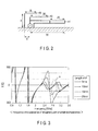
- FIG. 2 is a view showing an example of the antenna device shown in FIG. 1 ;
- FIG. 3 is a graph showing the frequency characteristics of the imaginary part of the antenna impedance of the antenna device shown in FIG. 2 ;
- FIGS. 4A , 4 B and 4 C are views showing a plurality of models obtained by changing the length of the parasitic element of the antenna device shown in FIG. 1 ;
- FIG. 5 is a graph showing the frequency characteristics of the imaginary parts of the antenna impedances based on the plurality of models shown in FIGS. 4A , 4 B and 4 C;
- FIG. 6 is a graph showing the VSWR frequency characteristics based on the plurality of models shown in FIGS. 4A , 4 B and 4 C;
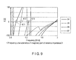
- FIG. 7 is a view for explaining one of the conditions for the antenna device shown in FIG. 1 ;
- FIGS. 8A , 8 B, 8 C and 8 D are views showing a plurality of models obtained by changing the length of the folded element of the antenna device shown in FIG. 7 ;
- FIG. 9 is a graph showing the frequency characteristics of the imaginary parts of antenna impedances based on the plurality of models shown in FIGS. 8A , 8 B, 8 C and 8 D;
- FIG. 10 is a view showing the arrangement of an antenna device according to the second embodiment.
- FIG. 11 is a view showing the arrangement of an antenna device according to the third embodiment.
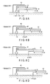
- FIG. 12 is a view showing an example of the antenna device shown in FIG. 11 ;
- FIG. 13 is a graph showing the frequency characteristics of the imaginary part of the antenna impedance in the example shown in FIG. 12 ;
- FIG. 14 is a graph showing VSWR frequency characteristics in the example shown in FIG. 12 ;
- FIG. 15 is a perspective view showing the arrangement of an antenna device according to the fourth embodiment.
- FIG. 16 is a perspective view showing the arrangement of an antenna device according to the fifth embodiment.
- FIG. 17 is a cross-sectional view of the antenna device shown in FIG. 16 ;
- FIG. 18 is a perspective view showing the arrangement of an antenna device according to the sixth embodiment.
- FIG. 19 is a graph showing the frequency characteristics of the imaginary part of the antenna impedance of the antenna device shown in FIG. 18 ;
- FIG. 20 is a graph showing the VSWR frequency characteristics of the antenna device shown in FIG. 18 ;
- FIG. 21 is a perspective view showing the arrangement of an antenna device according to the seventh embodiment.
- FIG. 22 is a graph showing the frequency characteristics of the imaginary part of the antenna impedance of the antenna device shown in FIG. 21 ;
- FIG. 23 is a graph showing the VSWR frequency characteristics of the antenna device shown in FIG. 21 ;
- FIG. 24 is a perspective view showing the arrangement of an antenna device according to the eighth embodiment.
- FIG. 25 is a graph showing the frequency characteristics of the imaginary part of the antenna impedance of the antenna device shown in FIG. 24 ;
- FIG. 26 is a graph showing the VSWR frequency characteristics of the antenna device shown in FIG. 24 ;
- FIG. 27 is a perspective view showing the arrangement of an antenna device according to the ninth embodiment.
- FIG. 28 is a graph showing the frequency characteristics of the imaginary part of the antenna impedance of the antenna device shown in FIG. 27 ;
- FIG. 29 is a graph showing the VSWR frequency characteristics of the antenna device shown in FIG. 27 ;
- FIG. 30 is a perspective view showing the arrangement of an antenna device according to the 10 th embodiment.
- FIG. 31 is a graph showing the frequency characteristics of the imaginary part of the antenna impedance of the antenna device shown in FIG. 30 ;
- FIG. 32 is a graph showing the VSWR frequency characteristics of the antenna device shown in FIG. 30 ;
- FIGS. 33A , 33 B, 33 C, 33 D and 33 E are views showing the first modification group of a folded element
- FIGS. 34A , 34 B, 34 C, 34 D and 34 E are views showing the second modification group of a folded element
- FIGS. 35A , 35 B, 35 C, 35 D and 35 E are views showing the first modification group of a monopole element
- FIGS. 36A , 36 B, 36 C and 36 D are views showing the second modification group of a monopole element
- FIGS. 37A , 37 B, 37 C, 37 D and 37 E are views showing the first modification group of a parasitic element
- FIGS. 38A , 38 B, 38 C and 38 D are views showing the second modification group of a parasitic element.
- FIGS. 39A and 39B are views showing a modification group to which the second parasitic element is added.
- an antenna device includes a first antenna element formed from a folded monopole element, a second antenna element formed from a monopole element, and a third antenna element formed from a parasitic element.
- One end of the first antenna element is connected to a feeding terminal, and the other end is connected to a first ground terminal.
- the first antenna element is folded in the middle, with a stub being provided between the forward and backward portions formed by folding.
- One end of the second antenna element is connected to the above feeding terminal directly or through part of the first antenna element, and the other end is open.
- One end of the third antenna element is connected to a second ground terminal provided at a position on the opposite side to the first ground terminal through the feeding terminal, and the other end is open.
- the electrical length of the first antenna element from the feeding terminal to the first ground terminal through the other end of the folding portion is set to nearly 1 ⁇ 2 a wavelength corresponding to a predetermined first resonance frequency.
- the electrical length of the second antenna element from the feeding terminal to the other end is set to nearly 1 ⁇ 4 a wavelength corresponding to a predetermined second resonance frequency.
- the third antenna element is placed parallel to the second antenna element in a state in which at least part of the third antenna element can be capacitively coupled to the second antenna element.
- the electrical length of the third antenna element from the second ground terminal to the other end is set to nearly 1 ⁇ 4 a wavelength corresponding to a predetermined third resonance frequency.
- the antenna device having the above arrangement can prevent the occurrence of parallel resonance between a plurality of series resonance bands. This can implement wider resonance bands.
- FIG. 1 is a view showing the arrangement of the main components of an electronic device including an antenna device according to the first embodiment.
- This electronic device includes a notebook personal computer or television receiver including a radio interface.
- the housing (not shown) of this device accommodates a printed circuit board 1 .
- the electronic device may be a portable terminal such as a cellular phone, smart phone, PDA (Personal Digital Assistant), or tablet type terminal other than a notebook personal computer or television receiver.
- the printed circuit board 1 may be formed as part of the metal housing or formed from a metal member such as a copper foil.
- the printed circuit board 1 includes a first area 1 a and a second area 1 b .
- the first area 1 a is provided with an antenna device 4 .
- a ground pattern 3 is formed in the second area 1 b .
- first and second ground terminals 31 and 32 are provided in the second area 1 b . Note that a plurality of circuit modules required to constitute an electronic device are mounted on the rear surface side of the printed circuit board 1 .
- the circuit module includes a radio unit 2 .
- the radio unit 2 has a function of transmitting and receiving radio signals by using the channel frequency assigned to a radio system as a communication target.
- the first area 1 a is provided with a feeding terminal 22 .
- the radio unit 2 is connected to the feeding terminal 22 through a feeding pattern 21 .
- the antenna device 4 has the following arrangement.
- the antenna device 4 includes a folded monopole element 41 as the first antenna element, a monopole element 42 as the second antenna element, and a parasitic element 43 as the third antenna element.
- the elements 41 , 42 and 43 are arranged such that the folded monopole element 41 is placed at a position nearest to the ground pattern 3 , and the monopole element 42 and the parasitic element 43 are placed outside the monopole element 41 in increasing order of distance from the ground pattern 3 .
- the folded monopole element 41 is formed from a conductive pattern having a shape obtained by folding the element in a hairpin form at a position dividing the entire element into almost two equal portions, with one end of the element being connected to the feeding terminal 22 , and the other end being connected to the first ground terminal 31 .
- a stub 411 is provided between the forward and backward portions formed by folding the element.
- the element length of the folded monopole element 41 that is, the electrical length from the feeding terminal 22 to the first ground terminal 31 through the folding position, is set to nearly 1 ⁇ 2 a wavelength corresponding to a predetermined first resonance frequency f 1 .
- the monopole element 42 is formed from an L-shaped conductive pattern having a proximal end connected to the feeding terminal 22 through part of the folded monopole element 41 , and a distal end open.
- the element length of the monopole element 42 that is, the electrical length from the feeding terminal 22 to the distal end, is set to nearly 1 ⁇ 4 a wavelength corresponding to a predetermined second resonance frequency f 2 .
- the parasitic element 43 is formed from an L-shaped conductive pattern having a proximal end connected to the ground terminal 32 , and a distal end open.
- the element length of the parasitic element 43 that is, the electrical length from the ground terminal 32 to the distal end, is set to a length nearly 1 ⁇ 4 a wavelength corresponding to a predetermined third resonance frequency f 3 .
- the parasitic element 43 is also placed parallel to the monopole element 42 such that at least part of the horizontal portion of the parasitic element 43 on the distal end side can be current-coupled to the horizontal portion of the monopole element 42 .
- the first resonance frequency f 1 is set in the band (700 MHz to 900 MHz) used by, for example, a radio system using LTE (Long Term Evolution).
- the second resonance frequency f 2 is set in the band (1.7 GHz to 1.9 GHz) used by a radio system based on the 3G standard.
- the third resonance frequency f 3 is set in a band near the first resonance frequency f 1 or the second resonance frequency f 2 to expand the band used by the above radio system using LTE or the band used by the radio system based on the 3G standard.
- FIG. 2 shows an example of an antenna device configured to satisfy this condition.
- the numbers in FIG. 2 represent the dimensions (unit: mm) of the respective antenna element portions.
- the parasitic element 43 In order to generate the third resonance frequency f 3 on the parasitic element 43 , the parasitic element 43 needs to be placed such that at least part of the distal end horizontal portion of the parasitic element 43 becomes parallel to the horizontal portion of the monopole element 42 .
- the present applicant analyzed the frequency characteristics of the imaginary parts of antenna impedances obtained when setting the distance (d in FIG. 2 ) between the feeding terminal 22 and the ground terminal 32 , to which the parasitic element 43 is grounded, to 5 mm, 10 mm, 15 mm, and 20 mm.
- FIG. 3 shows an example of the analysis result.
- the antenna device 4 of the first embodiment can independently adjust the third resonance frequency f 3 by changing the element length of the parasitic element 43 .
- the present applicant prepared three kinds of models 01, 02, and 03 obtained by setting the element length of the parasitic element 43 to different lengths as shown in, for example, FIGS. 4A , 4 B and 4 C and analyzed the frequency characteristics of the imaginary parts of the antenna impedances of the respective models and frequency characteristics of voltage standing wave ratio (VSWR).
- FIGS. 5 and 6 each show an example of each analysis result.
- setting the length of the horizontal portion of the parasitic element 43 to a relatively large value (e.g., 40 mm) as shown in FIG. 4A can generate the third resonance frequency f 3 in a low band K 31 (e.g., near 1.2 GHz).
- setting the length of the horizontal portion of the parasitic element 43 to a value (e.g., 27.5 mm) smaller than 40 mm as shown in FIG. 4B can generate the third resonance frequency f 3 in a band K 32 (near 2 GHz) higher than 1.2 GHz.
- K 1 and K 2 in FIG. 5 represent the first and second resonance frequencies f 1 and f 2 generated by the folded monopole element 41 and the monopole element 42 .
- the parasitic element 43 causes no interference with the folded monopole element 41 and the monopole element 42 . This is because the folded monopole element 41 , the monopole element 42 , and the parasitic element 43 are arranged in a positional relationship like that shown in FIG. 1 so as not to cause parallel resonance in bands between series resonances between the folded monopole element 41 , the monopole element 42 , and the parasitic element 43 , thereby preventing an increase in mismatch loss and deterioration in radiation efficiency.
- merely setting the element length of the parasitic element 43 to an arbitrary length can independently set the third resonance frequency f 3 in an arbitrary band near the first or second resonance frequency f 1 or f 2 without causing any interference between the folded monopole element 41 and the monopole element 42 .
- This can implement wider bands of the first or second resonance frequency f 1 or f 2 .
- a distance C between the first ground terminal 31 and the feeding terminal 22 of the folded monopole element 41 may be set to 1 ⁇ 5 or less a wavelength corresponding to the first resonance frequency f 1 as shown in FIG. 7 .
- the present applicant prepared four kinds of models, 04 to 07, obtained by changing the distance C as shown in, for example, FIGS. 8A , 8 B, 8 C and 8 D and analyzed the frequency characteristics of the imaginary parts of the antenna impedances of the respective models.
- FIG. 9 shows an example of the analysis result.
- the folded monopole element 41 with the stub, the monopole element 42 , and the parasitic element 43 are arranged in increasing order of distance from the ground pattern 3 , and the parasitic element 43 is placed so as to make at least part of its distal end horizontal portion become parallel to the horizontal portion of the monopole element 42 , thereby generating the third resonance frequency f 3 on the parasitic element 43 .
- merely setting the element length of the parasitic element 43 to an arbitrary length in the above manner can independently set the third resonance frequency f 3 in an arbitrary band near the first or second resonance frequency f 1 or f 2 without causing any interference between the folded monopole element 41 and the monopole element 42 .
- This can implement wider bands of the first or second resonance frequency f 1 or f 2 .
- FIG. 10 is a view showing the arrangement of an antenna device according to the second embodiment.
- the same reference numerals as in FIG. 10 denote the same parts in FIG. 1 , and a detailed description of them will be omitted.
- the section extending from the stub installation position to the folding position of a folded monopole element 41 with a stub is formed from one element 412 having a plate-like shape.
- the element 412 may have a rod-like shape other than a plate-like shape.
- This arrangement can increase the structural strength of the section of the folded monopole element 41 which extends from the stub to the folding position, and hence can increase the yield in manufacturing an antenna device 4 .
- FIG. 11 is a view showing the arrangement of an antenna device according to the third embodiment.
- the same reference numerals as in FIG. 11 denote the same parts in FIG. 1 , and a detailed description of them will be omitted.
- a folded monopole element 41 is formed by folding its section extending from the stub installation position to the folding position in a crank shape, with one additional element 44 being provided at a position corresponding to the root portion of the crank shape.
- FIG. 12 shows a specific arrangement of this monopole element.
- the numbers in FIG. 12 represent the dimensions (unit: mm) of the respective antenna element portions.
- FIGS. 13 and 14 show the results obtained by analyzing the frequency characteristics of the imaginary part of the antenna impedance and voltage standing wave ratio (VSWR) frequency characteristic.
- FIGS. 13 and 14 show also characteristics obtained without using the additional element 44 .
- providing the additional element 44 can also generate a resonance frequency at near 2.5 GHz. This allows the antenna device 4 to cope with a larger number of resonances. In addition, this can continuously expand the multiple resonance band from 2.0 GHz to 2.5 GHz.
- FIG. 15 is a view showing the arrangement of an antenna device according to the fourth embodiment.
- the same reference numerals as in FIG. 15 denote the same parts in FIG. 1 , and a detailed description of them will be omitted.
- a ground pattern 3 formed on a printed circuit board 1 has a side in a crank shape which is in contact with a first area 1 a .
- a feeding cable 23 is placed along a side of the portion on the ground pattern 3 which is formed into the crank shape so as to protrude into the first area 1 a .
- the feeding cable 23 is formed from a coaxial cable obtained by shielding a conductive line 24 , and the shielded line is grounded to a ground terminal 33 provided on the ground pattern 3 .
- a portion of the first area 1 a which protrudes into a second area 1 b by forming the ground pattern 3 into a crank shape is provided with a feeding terminal 22 .
- the distal end portion of the conductive line 24 of the feeding cable 23 is electrically connected to the feeding terminal 22 through a means such as soldering.
- This arrangement allows to place the feeding cable 23 along a side of the ground pattern 3 without forcibly bending the feeding cable 23 . This can improve the implementation efficiency of electronic components per unit area by effectively using the space of the printed circuit board 1 , thereby further improving the reliability of the device. In addition, this arrangement can prevent the feeding cable 23 from overlapping a parasitic element 43 , and hence can reduce variations in antenna characteristics owing to wiring of the feeding cable 23 .
- FIG. 16 is a perspective view showing the arrangement of an antenna device according to the fifth embodiment.
- FIG. 17 is a cross-sectional view of the antenna device shown in FIG. 16 .
- the same reference numerals as in FIG. 17 denote the same parts in FIG. 1 , and a detailed description of them will be omitted.
- the antenna device includes a resin antenna base material (resin base material) 5 .
- a folded monopole element 41 with a stub, a monopole element 42 , and a parasitic element 43 are arranged on the circumferential surface of the resin base material 5 .
- a printed circuit board 1 is formed from a flexible board. Conductive patterns respectively forming the folded monopole element 41 with the stub, the monopole element 42 , and the parasitic element 43 are formed in a first area 1 a of the printed circuit board 1 formed from this flexible board.
- the resin base material 5 is formed from a prismatic body having a longitudinal cross-section. As shown in FIG. 17 , the printed circuit board 1 formed from the above flexible board as shown in FIG. 17 is wound around the circumferential surface of the resin base material 5 formed from this prismatic body.
- FIG. 17 shows that the printed circuit board 1 is spaced apart from the circumferential surface of the resin base material 5 .
- the printed circuit board 1 is provided in tight contact with the resin base material 5 with an adhesive or bonding material such as a doubled-sided adhesive tape.
- an adhesive or bonding material such as a doubled-sided adhesive tape.
- a columnar body, an elliptic columnar body, or a plate-like body can be used instead of a prismatic body.
- This arrangement can decrease the dimensions of the printed circuit board 1 in a planar direction, and hence can downsize the antenna device 4 , that is, the electronic device.
- arranging the folded monopole element 41 with the stub, the monopole element 42 , and the parasitic element 43 on the circumferential surface of the resin base material 5 can provide a highly reliable device with structural stability.
- FIG. 18 is a perspective view showing the arrangement of an antenna device according to the sixth embodiment.
- the same reference numerals as in FIG. 18 denote the same parts in FIGS. 15 , 16 and 17 , and a detailed description of them will be omitted.
- Conductive patterns respectively forming a folded monopole element 41 with a stub, a monopole element 42 , and a parasitic element 43 are formed on a printed circuit board 1 formed from a flexible board.
- the folded monopole element 41 with the stub has a section extending from its stub installation position to the folding position, which is formed from one plate-like element 412 .
- the middle position of the monopole element 42 is connected to the folded monopole element 41 through a connecting element 424 .
- the proximal end portion of the parasitic element 43 is formed into a plate-like shape.
- power is fed to the folded monopole element 41 with the stub and the monopole element 42 via a feeding cable 23 formed from a coaxial cable.
- FIGS. 19 and 20 show an example of the results obtained by analyzing the frequency characteristics of the imaginary part of the antenna impedance and frequency characteristics of voltage standing wave ratio (VSWR) of the antenna device having the above arrangement.
- a first resonance K 1 occurs near 800 MHz owing to the folded monopole element 41 with the stub 411
- a third resonance K 3 occurs near 1.0 GHz at a position near the first resonance K 1 owing to the parasitic element 43 .
- This can expand the resonance band from 800 MHz to 1.0 GHz.
- a resonance K 2 occurs near 1.9 GHz owing to the monopole element 42 .
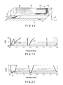
- FIG. 21 is a perspective view showing the arrangement of an antenna device according to the seventh embodiment.
- the same reference numerals as in FIG. 21 denote the same parts in FIGS. 15 , 16 , 17 and 18 , and a detailed description of them will be omitted.
- Conductive patterns respectively forming a folded monopole element 41 with a stub, a monopole element 42 , and a parasitic element 43 are formed on the printed circuit board 1 formed from a flexible substrate.
- the folded monopole element 41 with the stub has a section extending from its stub installation position to the folding position, which is formed from one plate-like element 412 .
- the plate-like element 412 has a width larger than that of the section extending from the stub installation position to a feeding terminal 22 .
- the parasitic element 43 has a planar proximal end portion.
- power is fed to the folded monopole element 41 with the stub and the monopole element 42 via a feeding cable 23 formed from a coaxial cable.
- FIGS. 22 and 23 show an example of the results obtained by analyzing the frequency characteristics of the imaginary part of the antenna impedance and frequency characteristics of voltage standing wave ratio (VSWR) by the antenna device having the above arrangement.
- a first resonance K 1 occurs near 900 MHz owing to the folded monopole element 41 with the stub.
- a second resonance K 2 occurs near 1.9 MHz owing to the monopole element 42
- a third resonance K 3 occurs near 2.3 GHz at a position adjacent to the second resonance K 2 owing to the parasitic element 43 . This can expand the resonance band from 1.9 GHz to 2.3 GHz.
- FIG. 24 is a perspective view showing the arrangement of an antenna device according to the eighth embodiment.
- the same reference numerals as in FIG. 24 denote the same parts in FIGS. 15 , 16 and 17 , and a detailed description of them will be omitted.
- Conductive patterns respectively forming a folded monopole element 41 with a stub, a monopole element 42 , and a parasitic element 43 are formed on the printed circuit board 1 formed from a flexible substrate.
- the folded monopole element 41 with the stub is formed by folding its section extending from the stub installation position to the folding position in a crank shape.
- the section extending from this stub installation position to the folding position is formed from one element 412 , and the element 412 has a width larger than the section extending from the stub installation position to a feeding terminal 22 .
- One additional element 44 is provided at a position corresponding to the root portion of the crank shape.
- the parasitic element 43 has a planar proximal end portion.
- power is fed to the folded monopole element 41 with the stub and the monopole element 42 via a feeding cable 23 formed from a coaxial cable.
- FIGS. 25 and 26 show an example of the results obtained by analyzing the frequency characteristics of the imaginary part of the antenna impedance and frequency characteristics of voltage standing wave ratio (VSWR) of the antenna device having the above arrangement.
- a first resonance K 1 occurs near 900 MHz owing to the folded monopole element 41 with the stub.
- a second resonance K 2 occurs near 2.0 GHz owing to the monopole element 42
- a third resonance K 3 occurs near 2.6 MHz at a position adjacent to the second resonance K 2 owing to the parasitic element 43 .
- This can expand the resonance band from 2.0 GHz to 2.6 GHz.
- a fourth resonance K 4 occurs near 3.2 GHz owing to the additional element 44 .
- this arrangement can provide a multiple resonance antenna device having a wide resonance band ranging from 2.0 GHz to 2.6 GHz.
- FIG. 27 is a perspective view showing the arrangement of an antenna device according to the ninth embodiment.
- the same reference numerals as in FIG. 27 denote the same parts in FIG. 24 , and a detailed description of them will be omitted.
- the ninth embodiment differs from the eighth embodiment in that a monopole element 42 has a longer element length.
- FIGS. 28 and 29 show an example of the results obtained by analyzing the frequency characteristics of the imaginary part of the antenna impedance and frequency characteristics of voltage standing wave ratio (VSWR) of the antenna device having the above arrangement.
- VSWR voltage standing wave ratio
- FIG. 30 is a perspective view showing the arrangement of an antenna device according to the 10th embodiment.
- the same reference numerals as in FIG. 30 denote the same parts in FIG. 18 , and a detailed description of them will be omitted.
- the 10th embodiment differs from the sixth embodiment in that a parasitic element 43 is branched midway into two elements 4371 and 4372 having different lengths, and the element 4371 , i.e., one of the elements 4371 and 4372 , has a plate-like distal end portion 433 .
- FIGS. 31 and 32 show an example of the results obtained by analyzing the frequency characteristics of the imaginary part of the antenna impedance and frequency characteristics of voltage standing wave ratio (VSWR) by the antenna device having the above arrangement.
- a first resonance K 1 occurs near 800 MHz owing to a folded monopole element 41 with a stub.
- a third resonance K 3 occurs near 1.0 GHz at a position near the first resonance K 1 owing to one parasitic element 4371 . This can expand the resonance band from 800 MHz to 1.0 GHz.
- a second resonance K 2 occurs near 1.9 GHz owing to a monopole element 42
- a fourth resonance K 4 occurs near 2.2 GHz at a position near the second resonance K 2 owing to the other parasitic element 4372 . This can expand the resonance band from 1.9 GHz to 2.2 GHz.
- FIGS. 33A , 33 B, 33 C, 33 D and 33 E and FIGS. 34A , 34 B, 34 C, 34 D and 34 E show various modifications of the folded monopole element 41 with the stub.
- the antenna device shown in FIG. 33A is configured such that the section extending from the installation position of the stub 411 of the folded monopole element 41 with the stub to the folding end is folded. This arrangement can reduce the installation space of the antenna device in the longitudinal direction of the folded monopole element 41 with the stub even if its element length is long.
- the antenna device shown in FIG. 33B has a plurality of (two in the case shown in FIG. 33B ) stubs 4111 and 4112 provided between the forward and backward portions of the folded monopole element 41 with the stub which are formed by folding. This arrangement can cause a larger number of resonances.
- the antenna device shown in FIG. 33C is configured such that the folded monopole element 41 with the stub has a wide portion near the feeding terminal 22 .
- the antenna device shown in FIG. 33D is configured such that the folded monopole element 41 with the stub has a wide portion near the first ground terminal 31 .
- the antenna device shown in FIG. 33E is configured such that the ground position of the folded monopole element 41 with the stub relative to the ground pattern 3 , i.e., the position of the first ground terminal 31 , is offset in the direction of the distal end of the folded monopole element 41 with the stub.
- the antenna device shown in FIG. 34A is configured such that the section extending from the installation position of the stub 411 of the folded monopole element 41 with the stub to the folding end is formed from one element, which is formed into a meandering shape.
- the antenna device shown in FIG. 34B is configured such that the portion between the middle portion and distal end portion of the section extending from the installation position of the stub 411 of the folded monopole element 41 with the stub to the folding end is formed from one element.
- the antenna device shown in FIG. 34C is configured such that the folded monopole element 41 with the stub and the monopole element 42 have a wide portion near the feeding terminal 22 .
- the antenna device shown in FIG. 34D is configured such that the portion between the middle portion and distal end portion of the section extending from the installation position of the stub 411 of the folded monopole element 41 with the stub to the folding end is formed from a wide plate-like element.
- the antenna device shown in FIG. 34E is configured such that lumped parameter elements 61 , 62 and 63 are respectively inserted in a portion near the feeding terminal 22 of the folded monopole element 41 with the stub and monopole element 42 , the interval from the branch position between the folded monopole element 41 with the stub and the monopole element 42 to the installation position of the stub 411 , and a portion near the first ground terminal 31 of the folded monopole element 41 with the stub.
- the lumped parameter elements 61 , 62 and 63 are formed from inductances and have a function of increasing the electrical length of the folded monopole element 41 with the stub.
- FIGS. 35A , 35 B, 35 C, 35 D and 35 E and FIGS. 36A , 36 B, 36 C and 36 D show various modifications of the monopole element 42 .
- the antenna device shown in FIG. 35A is configured such that the distal end portion of the monopole element 42 is folded. This makes it possible to reduce the installation space of the antenna device in the longitudinal direction of the monopole element 42 even if it has a long element length.
- the antenna device shown in FIG. 35B is configured such that the monopole element 42 has a wide distal end portion.
- the antenna device shown in FIG. 35C is configured such that the monopole element 42 is connected to the folded monopole element 41 with the stub through the connecting element 424 at a position where they are parallel to each other.
- the antenna device shown in FIG. 35D is configured such that the distal end portion of the monopole element 42 is branched to provide an additional element 425 . Note that the device shown in FIG. 35D is provided with only one additional element 425 . However, two or more additional elements may be provided.
- the antenna device shown in FIG. 35E is configured such that the monopole element 42 is branched at the feeding terminal 22 or at its nearby position without being branched midway along the folded monopole element 41 with the stub.
- the antenna device shown in FIG. 36A is configured such that the distal end portion of the monopole element 42 is formed into a meandering shape.
- the antenna device shown in FIG. 36B is configured such that a connecting portion 427 of the monopole element 42 for the folded monopole element 41 with the stub is formed into a wide portion.
- the antenna device shown in FIG. 36C is configured such that a second monopole element 428 is provided on the monopole element 42 in a direction opposite to the bending direction of the monopole element 42 .
- FIG. 36C shows a case in which one second monopole element 428 is provided, two or more second monopole elements may be provided.
- the antenna device shown in FIG. 36D is configured such that a lumped parameter element 64 is inserted in a portion near the connecting portion between the monopole element 42 and the folded monopole element 41 with the stub.
- the lumped parameter element 64 is formed from an inductance and has a function of increasing the electrical length of the monopole element 42 .
- FIGS. 37A , 37 B, 37 C, 37 D and 37 E and FIGS. 38A , 38 B, 38 C and 38 D show various modifications of the parasitic element 43 .
- the antenna device shown in FIG. 37A is configured such that the distal end portion of the parasitic element 43 is folded.
- the antenna device shown in FIG. 37B is configured such that the distal end portion of the parasitic element 43 is formed into a meandering shape. This makes it possible to reduce the installation space of the antenna device in the longitudinal direction of the parasitic element 43 even if it has a long element length.
- the antenna device shown in FIG. 37C is configured such that the parasitic element 43 has a wide distal end portion.
- the antenna device shown in FIG. 37D is configured such that the distal end portion of the parasitic element 43 is branched into a plurality of portions to provide a plurality of elements 4341 and 4342 .
- the distal end portion is branched into two portions.
- the distal end portion may be branched into three or more portions.
- the antenna device shown in FIG. 37E is configured such that a plurality of parasitic elements 43 and 45 are provided between the feeding terminal 22 and the second ground terminal 32 .
- the antenna device shown in FIG. 38A is configured such that the middle portion of the parasitic element 43 is formed into a meandering shape. This arrangement makes it possible to reduce the installation space of the antenna device in the longitudinal direction of the parasitic element 43 even if it has a long element length.
- the antenna device shown in FIG. 38B is configured such that the proximal end portion of the parasitic element 43 which is near the second ground terminal 32 is formed into a wide portion.
- the antenna device shown in FIG. 38C is configured such that the parasitic element 43 is branched into a plurality of portions at a position where it is bent in an L shape, thereby providing a plurality of elements 4371 and 4372 .
- the parasitic element 43 is branched into two portions.
- the parasitic element 43 may be branched into three or more portions.
- the antenna device shown in FIG. 38D is configured such that a lumped parameter element 65 is inserted in a portion near the connecting position between the parasitic element 43 and the second ground terminal 32 .
- the lumped parameter element 65 is formed from an inductance and has a function of increasing the electrical length of the parasitic element 43 .
- FIGS. 39A and 39B each show an example of the arrangement including an additional parasitic element.
- FIG. 39A shows an arrangement in which a second parasitic element 46 is placed between the ground pattern 3 and the folded monopole element 41 with the stub independently of the folded monopole element 41 with the stub.
- a second parasitic element 47 is placed between the ground pattern 3 and the folded monopole element 41 with the stub, and the ground terminal of the second parasitic element 47 is shared with the first ground terminal 31 of the folded monopole element 41 with the stub.
- the above arrangement can further increase the number of resonances and expand the band.
- the shapes, installation positions, sizes of the folded monopole element with the stub, monopole element, and parasitic element and the types, arrangements, and the like of the electronic device can be variously modified and embodied.
Landscapes
- Engineering & Computer Science (AREA)
- Computer Networks & Wireless Communication (AREA)
- Details Of Aerials (AREA)
- Support Of Aerials (AREA)
Abstract
Description
- This application is based upon and claims the benefit of priority from prior Japanese Patent Application No. 2011-076288, filed Mar. 30, 2011, the entire contents of which are incorporated herein by reference.
- Embodiments described herein relate generally to an antenna device and an electronic device including the antenna device.
- Recently, the housings of portable terminal devices typified by cellular phones, smart phones, Personal Digital Assistants (PDAs), and tablet type terminals have been required to reduce the dimensions and weight from the viewpoint of compactness and lightweightness. Accordingly, demands have arisen for more compact antenna devices. It has also been required to allow a single portable terminal device to communicate with a plurality of radio systems using different frequency bands.
- Conventionally, therefore, a multifrequency antenna device has been proposed, which has, for example, the second antenna element formed from a monopole element and provided in a direction opposite to the first antenna element formed from a folded element with a stub at a position near the feeding point of the first antenna element.
- In these conventionally provided multifrequency antenna devices, although it is possible to independently adjust the first resonance caused by the folded element and the second resonance caused by the monopole element, there occurs a band in which radiation efficiency deteriorates due to parallel resonance between the first resonance and the second resonance, resulting in difficulty in achieving wider bandwidth.
- A general architecture that implements the various features of the embodiments will now be described with reference to the drawings. The drawings and the associated descriptions are provided to illustrate the embodiments and not to limit the scope of the invention.
-
FIG. 1 is a view showing the arrangement of an electronic device including an antenna device according to the first embodiment; -
FIG. 2 is a view showing an example of the antenna device shown inFIG. 1 ; -
FIG. 3 is a graph showing the frequency characteristics of the imaginary part of the antenna impedance of the antenna device shown inFIG. 2 ; -
FIGS. 4A , 4B and 4C are views showing a plurality of models obtained by changing the length of the parasitic element of the antenna device shown inFIG. 1 ; -
FIG. 5 is a graph showing the frequency characteristics of the imaginary parts of the antenna impedances based on the plurality of models shown inFIGS. 4A , 4B and 4C; -
FIG. 6 is a graph showing the VSWR frequency characteristics based on the plurality of models shown inFIGS. 4A , 4B and 4C; -
FIG. 7 is a view for explaining one of the conditions for the antenna device shown inFIG. 1 ; -
FIGS. 8A , 8B, 8C and 8D are views showing a plurality of models obtained by changing the length of the folded element of the antenna device shown inFIG. 7 ; -
FIG. 9 is a graph showing the frequency characteristics of the imaginary parts of antenna impedances based on the plurality of models shown inFIGS. 8A , 8B, 8C and 8D; -
FIG. 10 is a view showing the arrangement of an antenna device according to the second embodiment; -
FIG. 11 is a view showing the arrangement of an antenna device according to the third embodiment; -
FIG. 12 is a view showing an example of the antenna device shown inFIG. 11 ; -
FIG. 13 is a graph showing the frequency characteristics of the imaginary part of the antenna impedance in the example shown inFIG. 12 ; -
FIG. 14 is a graph showing VSWR frequency characteristics in the example shown inFIG. 12 ; -
FIG. 15 is a perspective view showing the arrangement of an antenna device according to the fourth embodiment; -
FIG. 16 is a perspective view showing the arrangement of an antenna device according to the fifth embodiment; -
FIG. 17 is a cross-sectional view of the antenna device shown inFIG. 16 ; -
FIG. 18 is a perspective view showing the arrangement of an antenna device according to the sixth embodiment; -
FIG. 19 is a graph showing the frequency characteristics of the imaginary part of the antenna impedance of the antenna device shown inFIG. 18 ; -
FIG. 20 is a graph showing the VSWR frequency characteristics of the antenna device shown inFIG. 18 ; -
FIG. 21 is a perspective view showing the arrangement of an antenna device according to the seventh embodiment; -
FIG. 22 is a graph showing the frequency characteristics of the imaginary part of the antenna impedance of the antenna device shown inFIG. 21 ; -
FIG. 23 is a graph showing the VSWR frequency characteristics of the antenna device shown inFIG. 21 ; -
FIG. 24 is a perspective view showing the arrangement of an antenna device according to the eighth embodiment; -
FIG. 25 is a graph showing the frequency characteristics of the imaginary part of the antenna impedance of the antenna device shown inFIG. 24 ; -
FIG. 26 is a graph showing the VSWR frequency characteristics of the antenna device shown inFIG. 24 ; -
FIG. 27 is a perspective view showing the arrangement of an antenna device according to the ninth embodiment; -
FIG. 28 is a graph showing the frequency characteristics of the imaginary part of the antenna impedance of the antenna device shown inFIG. 27 ; -
FIG. 29 is a graph showing the VSWR frequency characteristics of the antenna device shown inFIG. 27 ; -
FIG. 30 is a perspective view showing the arrangement of an antenna device according to the 10th embodiment; -
FIG. 31 is a graph showing the frequency characteristics of the imaginary part of the antenna impedance of the antenna device shown inFIG. 30 ; -
FIG. 32 is a graph showing the VSWR frequency characteristics of the antenna device shown inFIG. 30 ; -
FIGS. 33A , 33B, 33C, 33D and 33E are views showing the first modification group of a folded element; -
FIGS. 34A , 34B, 34C, 34D and 34E are views showing the second modification group of a folded element; -
FIGS. 35A , 35B, 35C, 35D and 35E are views showing the first modification group of a monopole element; -
FIGS. 36A , 36B, 36C and 36D are views showing the second modification group of a monopole element; -
FIGS. 37A , 37B, 37C, 37D and 37E are views showing the first modification group of a parasitic element; -
FIGS. 38A , 38B, 38C and 38D are views showing the second modification group of a parasitic element; and -
FIGS. 39A and 39B are views showing a modification group to which the second parasitic element is added. - Various embodiments will be described hereinafter with reference to the accompanying drawings.
- In general, according to one embodiment, an antenna device includes a first antenna element formed from a folded monopole element, a second antenna element formed from a monopole element, and a third antenna element formed from a parasitic element.
- One end of the first antenna element is connected to a feeding terminal, and the other end is connected to a first ground terminal. The first antenna element is folded in the middle, with a stub being provided between the forward and backward portions formed by folding.
- One end of the second antenna element is connected to the above feeding terminal directly or through part of the first antenna element, and the other end is open.
- One end of the third antenna element is connected to a second ground terminal provided at a position on the opposite side to the first ground terminal through the feeding terminal, and the other end is open.
- The electrical length of the first antenna element from the feeding terminal to the first ground terminal through the other end of the folding portion is set to nearly ½ a wavelength corresponding to a predetermined first resonance frequency.
- The electrical length of the second antenna element from the feeding terminal to the other end is set to nearly ¼ a wavelength corresponding to a predetermined second resonance frequency.
- The third antenna element is placed parallel to the second antenna element in a state in which at least part of the third antenna element can be capacitively coupled to the second antenna element. The electrical length of the third antenna element from the second ground terminal to the other end is set to nearly ¼ a wavelength corresponding to a predetermined third resonance frequency.
- The antenna device having the above arrangement can prevent the occurrence of parallel resonance between a plurality of series resonance bands. This can implement wider resonance bands.
-
FIG. 1 is a view showing the arrangement of the main components of an electronic device including an antenna device according to the first embodiment. This electronic device includes a notebook personal computer or television receiver including a radio interface. The housing (not shown) of this device accommodates a printedcircuit board 1. - Note that the electronic device may be a portable terminal such as a cellular phone, smart phone, PDA (Personal Digital Assistant), or tablet type terminal other than a notebook personal computer or television receiver. The printed
circuit board 1 may be formed as part of the metal housing or formed from a metal member such as a copper foil. - The printed
circuit board 1 includes afirst area 1 a and asecond area 1 b. Thefirst area 1 a is provided with anantenna device 4. Aground pattern 3 is formed in thesecond area 1 b. In addition, first andsecond ground terminals second area 1 b. Note that a plurality of circuit modules required to constitute an electronic device are mounted on the rear surface side of the printedcircuit board 1. - The circuit module includes a
radio unit 2. Theradio unit 2 has a function of transmitting and receiving radio signals by using the channel frequency assigned to a radio system as a communication target. Thefirst area 1 a is provided with a feedingterminal 22. Theradio unit 2 is connected to the feedingterminal 22 through afeeding pattern 21. - The
antenna device 4 has the following arrangement. - The
antenna device 4 includes a foldedmonopole element 41 as the first antenna element, amonopole element 42 as the second antenna element, and aparasitic element 43 as the third antenna element. Theelements monopole element 41 is placed at a position nearest to theground pattern 3, and themonopole element 42 and theparasitic element 43 are placed outside themonopole element 41 in increasing order of distance from theground pattern 3. - The folded
monopole element 41 is formed from a conductive pattern having a shape obtained by folding the element in a hairpin form at a position dividing the entire element into almost two equal portions, with one end of the element being connected to the feedingterminal 22, and the other end being connected to thefirst ground terminal 31. Astub 411 is provided between the forward and backward portions formed by folding the element. The element length of the foldedmonopole element 41, that is, the electrical length from the feedingterminal 22 to thefirst ground terminal 31 through the folding position, is set to nearly ½ a wavelength corresponding to a predetermined first resonance frequency f1. - The
monopole element 42 is formed from an L-shaped conductive pattern having a proximal end connected to the feedingterminal 22 through part of the foldedmonopole element 41, and a distal end open. The element length of themonopole element 42, that is, the electrical length from the feedingterminal 22 to the distal end, is set to nearly ¼ a wavelength corresponding to a predetermined second resonance frequency f2. - The
parasitic element 43 is formed from an L-shaped conductive pattern having a proximal end connected to theground terminal 32, and a distal end open. The element length of theparasitic element 43, that is, the electrical length from theground terminal 32 to the distal end, is set to a length nearly ¼ a wavelength corresponding to a predetermined third resonance frequency f3. Theparasitic element 43 is also placed parallel to themonopole element 42 such that at least part of the horizontal portion of theparasitic element 43 on the distal end side can be current-coupled to the horizontal portion of themonopole element 42. - The first resonance frequency f1 is set in the band (700 MHz to 900 MHz) used by, for example, a radio system using LTE (Long Term Evolution). The second resonance frequency f2 is set in the band (1.7 GHz to 1.9 GHz) used by a radio system based on the 3G standard. The third resonance frequency f3 is set in a band near the first resonance frequency f1 or the second resonance frequency f2 to expand the band used by the above radio system using LTE or the band used by the radio system based on the 3G standard.
- The element lengths of the folded
monopole element 41 with the stub,monopole element 42, andparasitic element 43 and their relative positions are set to lengths that are necessary to generate the first, second, and third resonance frequencies f1, f2, and f3.FIG. 2 shows an example of an antenna device configured to satisfy this condition. The numbers inFIG. 2 represent the dimensions (unit: mm) of the respective antenna element portions. - In order to generate the third resonance frequency f3 on the
parasitic element 43, theparasitic element 43 needs to be placed such that at least part of the distal end horizontal portion of theparasitic element 43 becomes parallel to the horizontal portion of themonopole element 42. In order to check this condition, the present applicant analyzed the frequency characteristics of the imaginary parts of antenna impedances obtained when setting the distance (d inFIG. 2 ) between the feedingterminal 22 and theground terminal 32, to which theparasitic element 43 is grounded, to 5 mm, 10 mm, 15 mm, and 20 mm.FIG. 3 shows an example of the analysis result. - As is obvious from
FIG. 3 , when the distance d becomes larger than 15 mm, that is, the length of the portion of theparasitic element 43 which is parallel to themonopole element 42 becomes equal to or less than 0 mm, theparasitic element 43 cannot maintain a capacitively coupled state with themonopole element 42. As a consequence, it becomes impossible to cause resonance, as indicated by “A” inFIG. 3 . Obviously, therefore, it is necessary to place theparasitic element 43 so as to maintain a state in which at least the distal end portion of theparasitic element 43 is parallel to the horizontal portion of themonopole element 42. - In addition, the
antenna device 4 of the first embodiment can independently adjust the third resonance frequency f3 by changing the element length of theparasitic element 43. In order to check this effect, the present applicant prepared three kinds ofmodels parasitic element 43 to different lengths as shown in, for example,FIGS. 4A , 4B and 4C and analyzed the frequency characteristics of the imaginary parts of the antenna impedances of the respective models and frequency characteristics of voltage standing wave ratio (VSWR).FIGS. 5 and 6 each show an example of each analysis result. - As is obvious from the characteristics shown in
FIGS. 5 and 6 , setting the length of the horizontal portion of theparasitic element 43 to a relatively large value (e.g., 40 mm) as shown inFIG. 4A can generate the third resonance frequency f3 in a low band K31 (e.g., near 1.2 GHz). In addition, setting the length of the horizontal portion of theparasitic element 43 to a value (e.g., 27.5 mm) smaller than 40 mm as shown inFIG. 4B can generate the third resonance frequency f3 in a band K32 (near 2 GHz) higher than 1.2 GHz. Furthermore, setting the length of the horizontal portion of theparasitic element 43 to a value (e.g., 12.5 mm) shorter than 27.5 mm as shown inFIG. 4C can generate the third resonance frequency f3 in a band K33 (near 3.2 GHz) higher than 2 GHz. Note that K1 and K2 inFIG. 5 represent the first and second resonance frequencies f1 and f2 generated by the foldedmonopole element 41 and themonopole element 42. - The
parasitic element 43 causes no interference with the foldedmonopole element 41 and themonopole element 42. This is because the foldedmonopole element 41, themonopole element 42, and theparasitic element 43 are arranged in a positional relationship like that shown inFIG. 1 so as not to cause parallel resonance in bands between series resonances between the foldedmonopole element 41, themonopole element 42, and theparasitic element 43, thereby preventing an increase in mismatch loss and deterioration in radiation efficiency. - That is, according to the
antenna device 4 described above, merely setting the element length of theparasitic element 43 to an arbitrary length can independently set the third resonance frequency f3 in an arbitrary band near the first or second resonance frequency f1 or f2 without causing any interference between the foldedmonopole element 41 and themonopole element 42. This can implement wider bands of the first or second resonance frequency f1 or f2. - In order to effectively obtain the above effects, a distance C between the
first ground terminal 31 and the feedingterminal 22 of the foldedmonopole element 41 may be set to ⅕ or less a wavelength corresponding to the first resonance frequency f1 as shown inFIG. 7 . In order to check this condition, the present applicant prepared four kinds of models, 04 to 07, obtained by changing the distance C as shown in, for example,FIGS. 8A , 8B, 8C and 8D and analyzed the frequency characteristics of the imaginary parts of the antenna impedances of the respective models.FIG. 9 shows an example of the analysis result. - As is obvious from the analysis result shown in
FIG. 9 , in themodels 04 to 06 with the distance C being set to be relatively short, series resonances K11, K12 and K13 occur owing to the foldedmonopole element 41. However, in themodel 07 with the distance C being set to be long, no sufficient series resonance occurs, and hence the first resonance frequency f1 cannot be set. - As described in detail above, according to the first embodiment, the folded
monopole element 41 with the stub, themonopole element 42, and theparasitic element 43 are arranged in increasing order of distance from theground pattern 3, and theparasitic element 43 is placed so as to make at least part of its distal end horizontal portion become parallel to the horizontal portion of themonopole element 42, thereby generating the third resonance frequency f3 on theparasitic element 43. - Therefore, merely setting the element length of the
parasitic element 43 to an arbitrary length in the above manner can independently set the third resonance frequency f3 in an arbitrary band near the first or second resonance frequency f1 or f2 without causing any interference between the foldedmonopole element 41 and themonopole element 42. This can implement wider bands of the first or second resonance frequency f1 or f2. -
FIG. 10 is a view showing the arrangement of an antenna device according to the second embodiment. The same reference numerals as inFIG. 10 denote the same parts inFIG. 1 , and a detailed description of them will be omitted. - The section extending from the stub installation position to the folding position of a folded
monopole element 41 with a stub is formed from oneelement 412 having a plate-like shape. Note that theelement 412 may have a rod-like shape other than a plate-like shape. - This arrangement can increase the structural strength of the section of the folded
monopole element 41 which extends from the stub to the folding position, and hence can increase the yield in manufacturing anantenna device 4. -
FIG. 11 is a view showing the arrangement of an antenna device according to the third embodiment. The same reference numerals as inFIG. 11 denote the same parts inFIG. 1 , and a detailed description of them will be omitted. - A folded
monopole element 41 is formed by folding its section extending from the stub installation position to the folding position in a crank shape, with oneadditional element 44 being provided at a position corresponding to the root portion of the crank shape. -
FIG. 12 shows a specific arrangement of this monopole element. The numbers inFIG. 12 represent the dimensions (unit: mm) of the respective antenna element portions.FIGS. 13 and 14 show the results obtained by analyzing the frequency characteristics of the imaginary part of the antenna impedance and voltage standing wave ratio (VSWR) frequency characteristic.FIGS. 13 and 14 show also characteristics obtained without using theadditional element 44. - As is obvious from
FIGS. 13 and 14 , providing theadditional element 44 can also generate a resonance frequency at near 2.5 GHz. This allows theantenna device 4 to cope with a larger number of resonances. In addition, this can continuously expand the multiple resonance band from 2.0 GHz to 2.5 GHz. -
FIG. 15 is a view showing the arrangement of an antenna device according to the fourth embodiment. The same reference numerals as inFIG. 15 denote the same parts inFIG. 1 , and a detailed description of them will be omitted. - A
ground pattern 3 formed on a printedcircuit board 1 has a side in a crank shape which is in contact with afirst area 1 a. A feedingcable 23 is placed along a side of the portion on theground pattern 3 which is formed into the crank shape so as to protrude into thefirst area 1 a. The feedingcable 23 is formed from a coaxial cable obtained by shielding a conductive line 24, and the shielded line is grounded to aground terminal 33 provided on theground pattern 3. - In addition, a portion of the
first area 1 a which protrudes into asecond area 1 b by forming theground pattern 3 into a crank shape is provided with a feedingterminal 22. The distal end portion of the conductive line 24 of the feedingcable 23 is electrically connected to the feedingterminal 22 through a means such as soldering. - This arrangement allows to place the feeding
cable 23 along a side of theground pattern 3 without forcibly bending the feedingcable 23. This can improve the implementation efficiency of electronic components per unit area by effectively using the space of the printedcircuit board 1, thereby further improving the reliability of the device. In addition, this arrangement can prevent the feedingcable 23 from overlapping aparasitic element 43, and hence can reduce variations in antenna characteristics owing to wiring of the feedingcable 23. -
FIG. 16 is a perspective view showing the arrangement of an antenna device according to the fifth embodiment.FIG. 17 is a cross-sectional view of the antenna device shown inFIG. 16 . The same reference numerals as inFIG. 17 denote the same parts inFIG. 1 , and a detailed description of them will be omitted. - The antenna device according to the fifth embodiment includes a resin antenna base material (resin base material) 5. A folded
monopole element 41 with a stub, amonopole element 42, and aparasitic element 43 are arranged on the circumferential surface of theresin base material 5. - More specifically, a printed
circuit board 1 is formed from a flexible board. Conductive patterns respectively forming the foldedmonopole element 41 with the stub, themonopole element 42, and theparasitic element 43 are formed in afirst area 1 a of the printedcircuit board 1 formed from this flexible board. On the other hand, theresin base material 5 is formed from a prismatic body having a longitudinal cross-section. As shown inFIG. 17 , the printedcircuit board 1 formed from the above flexible board as shown inFIG. 17 is wound around the circumferential surface of theresin base material 5 formed from this prismatic body. - For the sake of illustrative convenience,
FIG. 17 shows that the printedcircuit board 1 is spaced apart from the circumferential surface of theresin base material 5. In practice, however, the printedcircuit board 1 is provided in tight contact with theresin base material 5 with an adhesive or bonding material such as a doubled-sided adhesive tape. As theresin base material 5, a columnar body, an elliptic columnar body, or a plate-like body can be used instead of a prismatic body. - This arrangement can decrease the dimensions of the printed
circuit board 1 in a planar direction, and hence can downsize theantenna device 4, that is, the electronic device. In addition, arranging the foldedmonopole element 41 with the stub, themonopole element 42, and theparasitic element 43 on the circumferential surface of theresin base material 5 can provide a highly reliable device with structural stability. -
FIG. 18 is a perspective view showing the arrangement of an antenna device according to the sixth embodiment. The same reference numerals as inFIG. 18 denote the same parts inFIGS. 15 , 16 and 17, and a detailed description of them will be omitted. - Conductive patterns respectively forming a folded
monopole element 41 with a stub, amonopole element 42, and aparasitic element 43 are formed on a printedcircuit board 1 formed from a flexible board. Of these elements, the foldedmonopole element 41 with the stub has a section extending from its stub installation position to the folding position, which is formed from one plate-like element 412. The middle position of themonopole element 42 is connected to the foldedmonopole element 41 through a connectingelement 424. The proximal end portion of theparasitic element 43 is formed into a plate-like shape. In addition, power is fed to the foldedmonopole element 41 with the stub and themonopole element 42 via a feedingcable 23 formed from a coaxial cable. -
FIGS. 19 and 20 show an example of the results obtained by analyzing the frequency characteristics of the imaginary part of the antenna impedance and frequency characteristics of voltage standing wave ratio (VSWR) of the antenna device having the above arrangement. According to this example, a first resonance K1 occurs near 800 MHz owing to the foldedmonopole element 41 with thestub 411, and a third resonance K3 occurs near 1.0 GHz at a position near the first resonance K1 owing to theparasitic element 43. This can expand the resonance band from 800 MHz to 1.0 GHz. In addition, a resonance K2 occurs near 1.9 GHz owing to themonopole element 42. -
FIG. 21 is a perspective view showing the arrangement of an antenna device according to the seventh embodiment. The same reference numerals as inFIG. 21 denote the same parts inFIGS. 15 , 16, 17 and 18, and a detailed description of them will be omitted. - Conductive patterns respectively forming a folded
monopole element 41 with a stub, amonopole element 42, and aparasitic element 43 are formed on the printedcircuit board 1 formed from a flexible substrate. Of these elements, the foldedmonopole element 41 with the stub has a section extending from its stub installation position to the folding position, which is formed from one plate-like element 412. The plate-like element 412 has a width larger than that of the section extending from the stub installation position to a feedingterminal 22. Theparasitic element 43 has a planar proximal end portion. In addition, power is fed to the foldedmonopole element 41 with the stub and themonopole element 42 via a feedingcable 23 formed from a coaxial cable. -
FIGS. 22 and 23 show an example of the results obtained by analyzing the frequency characteristics of the imaginary part of the antenna impedance and frequency characteristics of voltage standing wave ratio (VSWR) by the antenna device having the above arrangement. According to this example, a first resonance K1 occurs near 900 MHz owing to the foldedmonopole element 41 with the stub. A second resonance K2 occurs near 1.9 MHz owing to themonopole element 42, and a third resonance K3 occurs near 2.3 GHz at a position adjacent to the second resonance K2 owing to theparasitic element 43. This can expand the resonance band from 1.9 GHz to 2.3 GHz. -
FIG. 24 is a perspective view showing the arrangement of an antenna device according to the eighth embodiment. The same reference numerals as inFIG. 24 denote the same parts inFIGS. 15 , 16 and 17, and a detailed description of them will be omitted. - Conductive patterns respectively forming a folded
monopole element 41 with a stub, amonopole element 42, and aparasitic element 43 are formed on the printedcircuit board 1 formed from a flexible substrate. Of these elements, as shown inFIG. 11 , the foldedmonopole element 41 with the stub is formed by folding its section extending from the stub installation position to the folding position in a crank shape. The section extending from this stub installation position to the folding position is formed from oneelement 412, and theelement 412 has a width larger than the section extending from the stub installation position to a feedingterminal 22. - One
additional element 44 is provided at a position corresponding to the root portion of the crank shape. Theparasitic element 43 has a planar proximal end portion. In addition, power is fed to the foldedmonopole element 41 with the stub and themonopole element 42 via a feedingcable 23 formed from a coaxial cable. -
FIGS. 25 and 26 show an example of the results obtained by analyzing the frequency characteristics of the imaginary part of the antenna impedance and frequency characteristics of voltage standing wave ratio (VSWR) of the antenna device having the above arrangement. According to this example, a first resonance K1 occurs near 900 MHz owing to the foldedmonopole element 41 with the stub. A second resonance K2 occurs near 2.0 GHz owing to themonopole element 42, and a third resonance K3 occurs near 2.6 MHz at a position adjacent to the second resonance K2 owing to theparasitic element 43. This can expand the resonance band from 2.0 GHz to 2.6 GHz. In addition, a fourth resonance K4 occurs near 3.2 GHz owing to theadditional element 44. - That is, this arrangement can provide a multiple resonance antenna device having a wide resonance band ranging from 2.0 GHz to 2.6 GHz.
-
FIG. 27 is a perspective view showing the arrangement of an antenna device according to the ninth embodiment. The same reference numerals as inFIG. 27 denote the same parts inFIG. 24 , and a detailed description of them will be omitted. - The ninth embodiment differs from the eighth embodiment in that a
monopole element 42 has a longer element length. -
FIGS. 28 and 29 show an example of the results obtained by analyzing the frequency characteristics of the imaginary part of the antenna impedance and frequency characteristics of voltage standing wave ratio (VSWR) of the antenna device having the above arrangement. According to this example, it is possible to decrease the frequency of a second resonance K2 owing to themonopole element 42 to a frequency near 1.85 GHz. Therefore, the second resonance K2 owing to themonopole element 42 and a third resonance K3 owing to aparasitic element 43 can further expand a 2-GHz resonance band. -
FIG. 30 is a perspective view showing the arrangement of an antenna device according to the 10th embodiment. The same reference numerals as inFIG. 30 denote the same parts inFIG. 18 , and a detailed description of them will be omitted. - The 10th embodiment differs from the sixth embodiment in that a
parasitic element 43 is branched midway into twoelements element 4371, i.e., one of theelements distal end portion 433. -
FIGS. 31 and 32 show an example of the results obtained by analyzing the frequency characteristics of the imaginary part of the antenna impedance and frequency characteristics of voltage standing wave ratio (VSWR) by the antenna device having the above arrangement. According to this example, a first resonance K1 occurs near 800 MHz owing to a foldedmonopole element 41 with a stub. A third resonance K3 occurs near 1.0 GHz at a position near the first resonance K1 owing to oneparasitic element 4371. This can expand the resonance band from 800 MHz to 1.0 GHz. In addition, a second resonance K2 occurs near 1.9 GHz owing to amonopole element 42, and a fourth resonance K4 occurs near 2.2 GHz at a position near the second resonance K2 owing to the otherparasitic element 4372. This can expand the resonance band from 1.9 GHz to 2.2 GHz. - (1) Modification of Folded
Monopole Element 41 with Stub -
FIGS. 33A , 33B, 33C, 33D and 33E andFIGS. 34A , 34B, 34C, 34D and 34E show various modifications of the foldedmonopole element 41 with the stub. - The antenna device shown in
FIG. 33A is configured such that the section extending from the installation position of thestub 411 of the foldedmonopole element 41 with the stub to the folding end is folded. This arrangement can reduce the installation space of the antenna device in the longitudinal direction of the foldedmonopole element 41 with the stub even if its element length is long. - The antenna device shown in
FIG. 33B has a plurality of (two in the case shown inFIG. 33B )stubs monopole element 41 with the stub which are formed by folding. This arrangement can cause a larger number of resonances. - The antenna device shown in
FIG. 33C is configured such that the foldedmonopole element 41 with the stub has a wide portion near the feedingterminal 22. - The antenna device shown in
FIG. 33D is configured such that the foldedmonopole element 41 with the stub has a wide portion near thefirst ground terminal 31. - The antenna device shown in
FIG. 33E is configured such that the ground position of the foldedmonopole element 41 with the stub relative to theground pattern 3, i.e., the position of thefirst ground terminal 31, is offset in the direction of the distal end of the foldedmonopole element 41 with the stub. - The antenna device shown in
FIG. 34A is configured such that the section extending from the installation position of thestub 411 of the foldedmonopole element 41 with the stub to the folding end is formed from one element, which is formed into a meandering shape. - The antenna device shown in
FIG. 34B is configured such that the portion between the middle portion and distal end portion of the section extending from the installation position of thestub 411 of the foldedmonopole element 41 with the stub to the folding end is formed from one element. - The antenna device shown in
FIG. 34C is configured such that the foldedmonopole element 41 with the stub and themonopole element 42 have a wide portion near the feedingterminal 22. - The antenna device shown in
FIG. 34D is configured such that the portion between the middle portion and distal end portion of the section extending from the installation position of thestub 411 of the foldedmonopole element 41 with the stub to the folding end is formed from a wide plate-like element. - The antenna device shown in
FIG. 34E is configured such that lumpedparameter elements terminal 22 of the foldedmonopole element 41 with the stub andmonopole element 42, the interval from the branch position between the foldedmonopole element 41 with the stub and themonopole element 42 to the installation position of thestub 411, and a portion near thefirst ground terminal 31 of the foldedmonopole element 41 with the stub. The lumpedparameter elements monopole element 41 with the stub. - (2) Modification of
Monopole Element 42 -
FIGS. 35A , 35B, 35C, 35D and 35E andFIGS. 36A , 36B, 36C and 36D show various modifications of themonopole element 42. - The antenna device shown in
FIG. 35A is configured such that the distal end portion of themonopole element 42 is folded. This makes it possible to reduce the installation space of the antenna device in the longitudinal direction of themonopole element 42 even if it has a long element length. - The antenna device shown in
FIG. 35B is configured such that themonopole element 42 has a wide distal end portion. - The antenna device shown in
FIG. 35C is configured such that themonopole element 42 is connected to the foldedmonopole element 41 with the stub through the connectingelement 424 at a position where they are parallel to each other. - The antenna device shown in
FIG. 35D is configured such that the distal end portion of themonopole element 42 is branched to provide anadditional element 425. Note that the device shown inFIG. 35D is provided with only oneadditional element 425. However, two or more additional elements may be provided. - The antenna device shown in
FIG. 35E is configured such that themonopole element 42 is branched at the feedingterminal 22 or at its nearby position without being branched midway along the foldedmonopole element 41 with the stub. - The antenna device shown in
FIG. 36A is configured such that the distal end portion of themonopole element 42 is formed into a meandering shape. - The antenna device shown in
FIG. 36B is configured such that a connectingportion 427 of themonopole element 42 for the foldedmonopole element 41 with the stub is formed into a wide portion. - The antenna device shown in
FIG. 36C is configured such that asecond monopole element 428 is provided on themonopole element 42 in a direction opposite to the bending direction of themonopole element 42. AlthoughFIG. 36C shows a case in which onesecond monopole element 428 is provided, two or more second monopole elements may be provided. - The antenna device shown in
FIG. 36D is configured such that a lumpedparameter element 64 is inserted in a portion near the connecting portion between themonopole element 42 and the foldedmonopole element 41 with the stub. The lumpedparameter element 64 is formed from an inductance and has a function of increasing the electrical length of themonopole element 42. - (3) Modification of
Parasitic Element 43 -
FIGS. 37A , 37B, 37C, 37D and 37E andFIGS. 38A , 38B, 38C and 38D show various modifications of theparasitic element 43. - The antenna device shown in
FIG. 37A is configured such that the distal end portion of theparasitic element 43 is folded. - The antenna device shown in
FIG. 37B is configured such that the distal end portion of theparasitic element 43 is formed into a meandering shape. This makes it possible to reduce the installation space of the antenna device in the longitudinal direction of theparasitic element 43 even if it has a long element length. - The antenna device shown in
FIG. 37C is configured such that theparasitic element 43 has a wide distal end portion. - The antenna device shown in
FIG. 37D is configured such that the distal end portion of theparasitic element 43 is branched into a plurality of portions to provide a plurality ofelements FIG. 37D , the distal end portion is branched into two portions. However, the distal end portion may be branched into three or more portions. - The antenna device shown in
FIG. 37E is configured such that a plurality ofparasitic elements terminal 22 and thesecond ground terminal 32. - The antenna device shown in
FIG. 38A is configured such that the middle portion of theparasitic element 43 is formed into a meandering shape. This arrangement makes it possible to reduce the installation space of the antenna device in the longitudinal direction of theparasitic element 43 even if it has a long element length. - The antenna device shown in
FIG. 38B is configured such that the proximal end portion of theparasitic element 43 which is near thesecond ground terminal 32 is formed into a wide portion. - The antenna device shown in
FIG. 38C is configured such that theparasitic element 43 is branched into a plurality of portions at a position where it is bent in an L shape, thereby providing a plurality ofelements FIG. 38C , theparasitic element 43 is branched into two portions. However, theparasitic element 43 may be branched into three or more portions. - The antenna device shown in
FIG. 38D is configured such that a lumped parameter element 65 is inserted in a portion near the connecting position between theparasitic element 43 and thesecond ground terminal 32. The lumped parameter element 65 is formed from an inductance and has a function of increasing the electrical length of theparasitic element 43. - (4) When Parasitic Element Is Added
-
FIGS. 39A and 39B each show an example of the arrangement including an additional parasitic element. -
FIG. 39A shows an arrangement in which a secondparasitic element 46 is placed between theground pattern 3 and the foldedmonopole element 41 with the stub independently of the foldedmonopole element 41 with the stub. - Referring to
FIG. 39B , a secondparasitic element 47 is placed between theground pattern 3 and the foldedmonopole element 41 with the stub, and the ground terminal of the secondparasitic element 47 is shared with thefirst ground terminal 31 of the foldedmonopole element 41 with the stub. The above arrangement can further increase the number of resonances and expand the band. - In addition, the shapes, installation positions, sizes of the folded monopole element with the stub, monopole element, and parasitic element and the types, arrangements, and the like of the electronic device can be variously modified and embodied.
- While certain embodiments have been described, these embodiments have been presented by way of example only, and are not intended to limit the scope of the inventions. Indeed, the novel embodiments described herein may be embodied in a variety of other forms; furthermore, various omissions, substitutions and changes in the form of the embodiments described herein may be made without departing from the spirit of the inventions. The accompanying claims and their equivalents are intended to cover such forms or modifications as would fall within the scope and spirit of the inventions.
Claims (14)
Applications Claiming Priority (2)
| Application Number | Priority Date | Filing Date | Title |
|---|---|---|---|
| JP2011076288A JP5060629B1 (en) | 2011-03-30 | 2011-03-30 | ANTENNA DEVICE AND ELECTRONIC DEVICE HAVING THE ANTENNA DEVICE |
| JP2011-076288 | 2011-03-30 |
Publications (2)
| Publication Number | Publication Date |
|---|---|
| US20120249393A1 true US20120249393A1 (en) | 2012-10-04 |
| US8988292B2 US8988292B2 (en) | 2015-03-24 |
Family
ID=46926495
Family Applications (1)
| Application Number | Title | Priority Date | Filing Date |
|---|---|---|---|
| US13/345,283 Active 2033-03-22 US8988292B2 (en) | 2011-03-30 | 2012-01-06 | Antenna device and electronic device including antenna device |
Country Status (2)
| Country | Link |
|---|---|
| US (1) | US8988292B2 (en) |
| JP (1) | JP5060629B1 (en) |
Cited By (52)
| Publication number | Priority date | Publication date | Assignee | Title |
|---|---|---|---|---|
| US20120194390A1 (en) * | 2011-02-01 | 2012-08-02 | Natsumi Endo | Multiply resonant antenna device and electronic device including such and antenna device |
| US20130241777A1 (en) * | 2012-03-13 | 2013-09-19 | Auden Techno Corp. | Multi-band antenna structure |
| US20140071000A1 (en) * | 2012-09-13 | 2014-03-13 | Panasonic Corporation | Small antenna apparatus operable in multiple frequency bands |
| US20140078003A1 (en) * | 2012-09-18 | 2014-03-20 | Chiun Mai Communication Systems, Inc. | Antenna module and wireless communication device |
| WO2014059629A1 (en) * | 2012-10-17 | 2014-04-24 | 华为终端有限公司 | Multimode wideband antenna module and wireless terminal |
| US20140118204A1 (en) * | 2012-11-01 | 2014-05-01 | Nvidia Corporation | Antenna integrated with metal chassis |
| CN103928748A (en) * | 2013-01-16 | 2014-07-16 | 宏碁股份有限公司 | communication device |
| US20140285391A1 (en) * | 2013-03-15 | 2014-09-25 | Ruckus Wireless, Inc. | Low-band reflector for dual band directional antenna |
| WO2014147027A1 (en) * | 2013-03-20 | 2014-09-25 | Aviwest | Antenna formed by at least two radiating strands and a ground plane |
| US20150097733A1 (en) * | 2013-10-04 | 2015-04-09 | Wistron Neweb Corporation | Antenna |
| CN104577298A (en) * | 2013-10-22 | 2015-04-29 | 宏碁股份有限公司 | Communication device |
| CN104838539A (en) * | 2012-10-26 | 2015-08-12 | 诺基亚技术有限公司 | Loop antenna having a parasitically coupled element |
| US20150236422A1 (en) * | 2014-02-20 | 2015-08-20 | Wistron Neweb Corporation | Broadband antenna |
| CN104868248A (en) * | 2014-02-26 | 2015-08-26 | 启碁科技股份有限公司 | Broadband antenna |
| US20150364820A1 (en) * | 2014-06-13 | 2015-12-17 | Qualcomm Incorporated | Multiband antenna apparatus and methods |
| US9231304B2 (en) | 2014-01-21 | 2016-01-05 | Nvidia Corporation | Wideband loop antenna and an electronic device including the same |
| EP2950392A4 (en) * | 2013-01-28 | 2016-01-20 | Panasonic Ip Man Co Ltd | Antenna device |
| EP2993732A1 (en) * | 2014-08-28 | 2016-03-09 | Kabushiki Kaisha Toshiba | Antenna apparatus and electronic device including the antenna apparatus |
| US9368862B2 (en) | 2014-01-21 | 2016-06-14 | Nvidia Corporation | Wideband antenna and an electronic device including the same |
| US20160190688A1 (en) * | 2014-12-31 | 2016-06-30 | Fih (Hong Kong) Limited | Antenna structure and wireless communication device using same |
| US20160190689A1 (en) * | 2014-12-31 | 2016-06-30 | Fih (Hong Kong) Limited | Antenna structure and wireless communication device using same |
| CN105789820A (en) * | 2014-12-23 | 2016-07-20 | 深圳富泰宏精密工业有限公司 | Antenna structure and wireless communication device with same |
| CN105811082A (en) * | 2014-12-31 | 2016-07-27 | 深圳富泰宏精密工业有限公司 | Antenna structure and radio communication device provided with antenna structure |
| US20160329627A1 (en) * | 2013-12-23 | 2016-11-10 | Emw Co., Ltd. | Embedded antenna |
| US9509048B2 (en) | 2014-08-28 | 2016-11-29 | Kabushiki Kaisha Toshiba | Antenna apparatus and electronic device including the antenna apparatus |
| EP3116063A1 (en) * | 2015-07-08 | 2017-01-11 | Climas Technology Co., Ltd. | Antenna system and a communication device |
| US9570803B2 (en) * | 2012-08-08 | 2017-02-14 | Canon Kabushiki Kaisha | Multi-band antenna |
| US9577339B2 (en) | 2013-05-31 | 2017-02-21 | Kabushiki Kaisha Toshiba | Antenna device and electronic device |
| EP3136506A1 (en) * | 2015-08-26 | 2017-03-01 | Acer Incorporated | Communication device |
| US9595759B2 (en) | 2014-01-21 | 2017-03-14 | Nvidia Corporation | Single element dual-feed antennas and an electronic device including the same |
| CN106505292A (en) * | 2015-09-06 | 2017-03-15 | 宏碁股份有限公司 | Communication device |
| CN106654527A (en) * | 2016-12-20 | 2017-05-10 | 西安易朴通讯技术有限公司 | Planar antenna and terminal equipment |
| CN106716715A (en) * | 2014-10-02 | 2017-05-24 | 旭硝子株式会社 | Antenna device and wireless device |
| US20170229762A1 (en) * | 2014-10-24 | 2017-08-10 | Hewlett-Packard Development Company, Lp. | Mobile computing device antenna |
| TWI628866B (en) * | 2013-12-31 | 2018-07-01 | 群邁通訊股份有限公司 | Antenna structure and wireless communication device having the same |
| US20180233817A1 (en) * | 2015-10-14 | 2018-08-16 | Murata Manufacturing Co., Ltd. | Antenna device |
| KR101918990B1 (en) | 2012-05-09 | 2018-11-16 | 엘지전자 주식회사 | Antenna apparatus and mobile terminal having the same |
| TWI652854B (en) | 2014-10-31 | 2019-03-01 | 群邁通訊股份有限公司 | Antenna structure and wireless communication device having the same |
| CN109478722A (en) * | 2016-07-22 | 2019-03-15 | 微软技术许可有限责任公司 | Antenna with multiple resonant coupling loops |
| US11211715B2 (en) * | 2017-04-28 | 2021-12-28 | Suguru Kojima | Antenna apparatus and mobile terminal |
| US11276938B2 (en) * | 2018-01-11 | 2022-03-15 | Semtech Corporation | Single layer antenna |
| US20220158348A1 (en) * | 2020-11-18 | 2022-05-19 | Realtek Semiconductor Corporation | Wireless communication apparatus and printed dual band antenna thereof |
| CN114552170A (en) * | 2020-11-25 | 2022-05-27 | 瑞昱半导体股份有限公司 | Wireless communication device and printed dual-band antenna thereof |
| CN115296013A (en) * | 2022-08-04 | 2022-11-04 | 荣耀终端有限公司 | Antenna assembly and electronic equipment |
| CN115764268A (en) * | 2022-11-01 | 2023-03-07 | 歌尔股份有限公司 | Antennas and Electronics |
| CN116231273A (en) * | 2021-12-06 | 2023-06-06 | Oppo广东移动通信有限公司 | Electronic equipment |
| US11862838B2 (en) * | 2020-04-17 | 2024-01-02 | Apple Inc. | Electronic devices having wideband antennas |
| WO2024060479A1 (en) * | 2022-09-21 | 2024-03-28 | 荣耀终端有限公司 | Foldable electronic device |
| EP4372914A1 (en) * | 2022-11-21 | 2024-05-22 | Wistron Corporation | Antenna module |
| CN119315250A (en) * | 2023-07-14 | 2025-01-14 | Oppo广东移动通信有限公司 | Foldable electronic devices |
| US12206163B2 (en) | 2020-09-01 | 2025-01-21 | Apple Inc. | Electronic devices having antennas that radiate through three-dimensionally curved cover layers |
| US20250149797A1 (en) * | 2023-11-03 | 2025-05-08 | Pegatron Corporation | Antenna module |
Families Citing this family (6)
| Publication number | Priority date | Publication date | Assignee | Title |
|---|---|---|---|---|
| US9356336B1 (en) * | 2012-06-13 | 2016-05-31 | Amazon Technologies Inc. | Dual-folded monopole antenna (DFMA) |
| TWI581505B (en) * | 2012-10-26 | 2017-05-01 | 群邁通訊股份有限公司 | Antenna structure |
| JP6701351B2 (en) * | 2015-12-31 | 2020-05-27 | 華為技術有限公司Huawei Technologies Co.,Ltd. | Antenna device and terminal |
| CN107591624B (en) * | 2017-08-17 | 2020-08-11 | 海信视像科技股份有限公司 | Antenna and television terminal |
| TWM568509U (en) * | 2018-07-12 | 2018-10-11 | 明泰科技股份有限公司 | Antenna module with low profile and high dual band insulation |
| TWI768865B (en) * | 2021-05-03 | 2022-06-21 | 和碩聯合科技股份有限公司 | Antenna module and electronic device |
Citations (7)
| Publication number | Priority date | Publication date | Assignee | Title |
|---|---|---|---|---|
| US6407710B2 (en) * | 2000-04-14 | 2002-06-18 | Tyco Electronics Logistics Ag | Compact dual frequency antenna with multiple polarization |
| US6639560B1 (en) * | 2002-04-29 | 2003-10-28 | Centurion Wireless Technologies, Inc. | Single feed tri-band PIFA with parasitic element |
| US6930641B2 (en) * | 2000-06-08 | 2005-08-16 | Matsushita Electric Industrial Co., Ltd. | Antenna and radio device using the same |
| US7319432B2 (en) * | 2002-03-14 | 2008-01-15 | Sony Ericsson Mobile Communications Ab | Multiband planar built-in radio antenna with inverted-L main and parasitic radiators |
| US8063827B2 (en) * | 2008-01-30 | 2011-11-22 | Kabushiki Kaisha Toshiba | Antenna device and radio apparatus operable in multiple frequency bands |
| US8098211B2 (en) * | 2006-12-22 | 2012-01-17 | Murata Manufacturing Co., Ltd. | Antenna structure and radio communication apparatus including the same |
| US8717241B2 (en) * | 2007-08-20 | 2014-05-06 | Ethertronics, Inc. | Antenna with active elements |
Family Cites Families (53)
| Publication number | Priority date | Publication date | Assignee | Title |
|---|---|---|---|---|
| JP3340621B2 (en) | 1996-05-13 | 2002-11-05 | 松下電器産業株式会社 | Planar antenna |
| JPH1079622A (en) | 1996-09-02 | 1998-03-24 | Matsushita Electric Ind Co Ltd | Frequency sharing antenna |
| JP3347093B2 (en) | 1999-06-10 | 2002-11-20 | 埼玉日本電気株式会社 | Portable wireless device and terminal matching switching method |
| JP2003273643A (en) | 2002-03-18 | 2003-09-26 | Ntt Docomo Inc | Dipole antenna device with reflector |
| JP3656610B2 (en) | 2002-03-27 | 2005-06-08 | 日立電線株式会社 | Plate-like antenna and electric device having the same |
| US6624789B1 (en) | 2002-04-11 | 2003-09-23 | Nokia Corporation | Method and system for improving isolation in radio-frequency antennas |
| JP3828050B2 (en) | 2002-06-14 | 2006-09-27 | 株式会社東芝 | Antenna array and wireless device |
| JP3925364B2 (en) | 2002-09-03 | 2007-06-06 | 株式会社豊田中央研究所 | Antenna and diversity receiver |
| JP2004201278A (en) | 2002-12-06 | 2004-07-15 | Sharp Corp | Pattern antenna |
| ATE456194T1 (en) | 2003-07-22 | 2010-02-15 | Nxp Bv | ANTENNA SWITCH WITH ADAPTIVE FILTER |
| JP2005136572A (en) | 2003-10-29 | 2005-05-26 | Renesas Technology Corp | Semiconductor integrated circuit for wireless communication, semiconductor integrated circuit for data processing, and portable terminal |
| JP2005295493A (en) | 2004-03-12 | 2005-10-20 | Mitsubishi Materials Corp | Antenna device |
| JP3805772B2 (en) | 2004-01-13 | 2006-08-09 | 株式会社東芝 | ANTENNA DEVICE AND PORTABLE RADIO COMMUNICATION DEVICE |
| US7403160B2 (en) | 2004-06-17 | 2008-07-22 | Interdigital Technology Corporation | Low profile smart antenna for wireless applications and associated methods |
| JP2006042111A (en) | 2004-07-29 | 2006-02-09 | Matsushita Electric Ind Co Ltd | Antenna device |
| JP2006101486A (en) | 2004-08-30 | 2006-04-13 | Mitsubishi Materials Corp | Wireless communication module and wireless communication device |
| JP2006166994A (en) | 2004-12-13 | 2006-06-29 | Heiwa Corp | Inspection apparatus of ball detector |
| JP3775795B1 (en) | 2005-01-11 | 2006-05-17 | 株式会社東芝 | Wireless device |
| JP2006238269A (en) * | 2005-02-28 | 2006-09-07 | Hoko Denshi Kk | Inverted LFL antenna and method of constructing inverted LFL antenna |
| JP2006279530A (en) | 2005-03-29 | 2006-10-12 | Toshiba Corp | ANTENNA DEVICE AND PORTABLE ELECTRONIC DEVICE HAVING THE ANTENNA DEVICE |
| JP2007123982A (en) | 2005-10-25 | 2007-05-17 | Sony Ericsson Mobilecommunications Japan Inc | Multiband compatible antenna system and communication terminal |
| JP2007129597A (en) * | 2005-11-07 | 2007-05-24 | Nissei Electric Co Ltd | Multi-frequency antenna |
| JP4231867B2 (en) | 2005-11-18 | 2009-03-04 | 株式会社東芝 | Wireless device and electronic device |
| TWM293545U (en) | 2006-01-13 | 2006-07-01 | Cameo Communications Inc | Patch antenna, and wireless networking device with the same |
| WO2007090062A2 (en) | 2006-01-27 | 2007-08-09 | Airgain, Inc. | Dual band antenna |
| US7450072B2 (en) | 2006-03-28 | 2008-11-11 | Qualcomm Incorporated | Modified inverted-F antenna for wireless communication |
| JP4146478B2 (en) | 2006-07-07 | 2008-09-10 | 株式会社東芝 | Wireless module and portable terminal |
| JP2008028734A (en) | 2006-07-21 | 2008-02-07 | Hitachi Metals Ltd | Surface mounting antenna and communication apparatus mounting it |
| EP2048739A4 (en) | 2006-07-28 | 2009-08-05 | Murata Manufacturing Co | Antenna device and radio communication device |
| JP4747988B2 (en) | 2006-08-07 | 2011-08-17 | 株式会社デンソー | In-vehicle antenna device and manufacturing method thereof |
| JP2008160411A (en) | 2006-12-22 | 2008-07-10 | Toshiba Corp | Antenna device and portable radio |
| JP4864733B2 (en) | 2007-01-16 | 2012-02-01 | 株式会社東芝 | Antenna device |
| TWI396331B (en) | 2007-04-17 | 2013-05-11 | Quanta Comp Inc | Dual frequency antenna |
| JP2008271468A (en) | 2007-04-25 | 2008-11-06 | Toshiba Corp | Antenna device |
| KR100964652B1 (en) | 2007-05-03 | 2010-06-22 | 주식회사 이엠따블유 | Multiband Antenna and Wireless Communication Device Including the Same |
| JP4830146B2 (en) | 2007-05-10 | 2011-12-07 | 望 長谷部 | Unidirectional antenna |
| JP4738380B2 (en) | 2007-05-10 | 2011-08-03 | 株式会社東芝 | Electronics |
| RU2009148235A (en) | 2007-07-05 | 2011-08-10 | Мицубиси Кейбл Индастриз, Лтд. (JP) | ANTENNA DEVICE |
| JP4966125B2 (en) | 2007-07-27 | 2012-07-04 | 株式会社東芝 | Antenna device and radio |
| JP4643624B2 (en) * | 2007-09-21 | 2011-03-02 | 株式会社東芝 | ANTENNA DEVICE AND ELECTRONIC DEVICE |
| JP2009100602A (en) | 2007-10-18 | 2009-05-07 | Yamaha Corp | Dc-dc converter |
| JP5221115B2 (en) | 2007-11-30 | 2013-06-26 | 三菱電線工業株式会社 | Antenna device |
| US7916089B2 (en) | 2008-01-04 | 2011-03-29 | Apple Inc. | Antenna isolation for portable electronic devices |
| JP2009246560A (en) | 2008-03-28 | 2009-10-22 | Ngk Spark Plug Co Ltd | Antenna device and radio communication apparatus with the same |
| KR100981883B1 (en) | 2008-04-30 | 2010-09-14 | 주식회사 에이스테크놀로지 | Broadband Internal Antenna Using Delayed Wave Structure |
| JP4197734B2 (en) | 2008-05-26 | 2008-12-17 | 株式会社東芝 | Wireless module |
| JP2010041071A (en) | 2008-07-31 | 2010-02-18 | Toshiba Corp | Antenna device |
| JP5304220B2 (en) | 2008-12-24 | 2013-10-02 | 富士通株式会社 | Antenna device, printed circuit board including antenna device, and wireless communication device including antenna device |
| JP5603020B2 (en) * | 2009-03-26 | 2014-10-08 | 日本電気株式会社 | Antenna device |
| WO2011024280A1 (en) | 2009-08-27 | 2011-03-03 | 株式会社 東芝 | Antenna device and communication device |
| US8228242B2 (en) | 2009-09-25 | 2012-07-24 | Sony Ericsson Mobile Communications Ab | Ultra wide band secondary antennas and wireless devices using the same |
| JP5127966B1 (en) | 2011-08-30 | 2013-01-23 | 株式会社東芝 | ANTENNA DEVICE AND ELECTRONIC DEVICE HAVING THE ANTENNA DEVICE |
| JP5162012B1 (en) | 2011-08-31 | 2013-03-13 | 株式会社東芝 | ANTENNA DEVICE AND ELECTRONIC DEVICE HAVING THE ANTENNA DEVICE |
-
2011
- 2011-03-30 JP JP2011076288A patent/JP5060629B1/en active Active
-
2012
- 2012-01-06 US US13/345,283 patent/US8988292B2/en active Active
Patent Citations (7)
| Publication number | Priority date | Publication date | Assignee | Title |
|---|---|---|---|---|
| US6407710B2 (en) * | 2000-04-14 | 2002-06-18 | Tyco Electronics Logistics Ag | Compact dual frequency antenna with multiple polarization |
| US6930641B2 (en) * | 2000-06-08 | 2005-08-16 | Matsushita Electric Industrial Co., Ltd. | Antenna and radio device using the same |
| US7319432B2 (en) * | 2002-03-14 | 2008-01-15 | Sony Ericsson Mobile Communications Ab | Multiband planar built-in radio antenna with inverted-L main and parasitic radiators |
| US6639560B1 (en) * | 2002-04-29 | 2003-10-28 | Centurion Wireless Technologies, Inc. | Single feed tri-band PIFA with parasitic element |
| US8098211B2 (en) * | 2006-12-22 | 2012-01-17 | Murata Manufacturing Co., Ltd. | Antenna structure and radio communication apparatus including the same |
| US8717241B2 (en) * | 2007-08-20 | 2014-05-06 | Ethertronics, Inc. | Antenna with active elements |
| US8063827B2 (en) * | 2008-01-30 | 2011-11-22 | Kabushiki Kaisha Toshiba | Antenna device and radio apparatus operable in multiple frequency bands |
Cited By (78)
| Publication number | Priority date | Publication date | Assignee | Title |
|---|---|---|---|---|
| US8779987B2 (en) * | 2011-02-01 | 2014-07-15 | Kabushiki Kaisha Toshiba | Multiply resonant antenna device and electronic device including such and antenna device |
| US20120194390A1 (en) * | 2011-02-01 | 2012-08-02 | Natsumi Endo | Multiply resonant antenna device and electronic device including such and antenna device |
| US20130241777A1 (en) * | 2012-03-13 | 2013-09-19 | Auden Techno Corp. | Multi-band antenna structure |
| KR101918990B1 (en) | 2012-05-09 | 2018-11-16 | 엘지전자 주식회사 | Antenna apparatus and mobile terminal having the same |
| US9570803B2 (en) * | 2012-08-08 | 2017-02-14 | Canon Kabushiki Kaisha | Multi-band antenna |
| US9698480B2 (en) * | 2012-09-13 | 2017-07-04 | Panasonic Intellectual Property Management Co., Ltd. | Small antenna apparatus operable in multiple frequency bands |
| US20140071000A1 (en) * | 2012-09-13 | 2014-03-13 | Panasonic Corporation | Small antenna apparatus operable in multiple frequency bands |
| US20140078003A1 (en) * | 2012-09-18 | 2014-03-20 | Chiun Mai Communication Systems, Inc. | Antenna module and wireless communication device |
| WO2014059629A1 (en) * | 2012-10-17 | 2014-04-24 | 华为终端有限公司 | Multimode wideband antenna module and wireless terminal |
| US9300041B2 (en) | 2012-10-17 | 2016-03-29 | Huawei Device Co., Ltd. | Multimode broadband antenna module and wireless terminal |
| EP2912718A4 (en) * | 2012-10-26 | 2016-05-04 | Nokia Technologies Oy | Loop antenna having a parasitically coupled element |
| US9484633B2 (en) | 2012-10-26 | 2016-11-01 | Nokia Technologies Oy | Loop antenna having a parasitically coupled element |
| CN104838539A (en) * | 2012-10-26 | 2015-08-12 | 诺基亚技术有限公司 | Loop antenna having a parasitically coupled element |
| US9172136B2 (en) | 2012-11-01 | 2015-10-27 | Nvidia Corporation | Multi-band antenna and an electronic device including the same |
| US9812770B2 (en) * | 2012-11-01 | 2017-11-07 | Nvidia Corporation | Antenna integrated with metal chassis |
| US20140118204A1 (en) * | 2012-11-01 | 2014-05-01 | Nvidia Corporation | Antenna integrated with metal chassis |
| CN103928748A (en) * | 2013-01-16 | 2014-07-16 | 宏碁股份有限公司 | communication device |
| US9692140B2 (en) | 2013-01-28 | 2017-06-27 | Panasonic Intellectual Property Management Co., Ltd. | Antenna apparatus capable of reducing decreases in gain and bandwidth |
| EP2950392A4 (en) * | 2013-01-28 | 2016-01-20 | Panasonic Ip Man Co Ltd | Antenna device |
| US10230161B2 (en) * | 2013-03-15 | 2019-03-12 | Arris Enterprises Llc | Low-band reflector for dual band directional antenna |
| US20140285391A1 (en) * | 2013-03-15 | 2014-09-25 | Ruckus Wireless, Inc. | Low-band reflector for dual band directional antenna |
| FR3003698A1 (en) * | 2013-03-20 | 2014-09-26 | Aviwest | ANTENNA CONSISTING OF AT LEAST TWO RADIANT BRINS AND A MASS PLAN. |
| WO2014147027A1 (en) * | 2013-03-20 | 2014-09-25 | Aviwest | Antenna formed by at least two radiating strands and a ground plane |
| US9577339B2 (en) | 2013-05-31 | 2017-02-21 | Kabushiki Kaisha Toshiba | Antenna device and electronic device |
| US20150097733A1 (en) * | 2013-10-04 | 2015-04-09 | Wistron Neweb Corporation | Antenna |
| CN104577298A (en) * | 2013-10-22 | 2015-04-29 | 宏碁股份有限公司 | Communication device |
| US10622704B2 (en) * | 2013-12-23 | 2020-04-14 | Emw Co., Ltd. | Embedded antenna |
| US20160329627A1 (en) * | 2013-12-23 | 2016-11-10 | Emw Co., Ltd. | Embedded antenna |
| TWI628866B (en) * | 2013-12-31 | 2018-07-01 | 群邁通訊股份有限公司 | Antenna structure and wireless communication device having the same |
| US9231304B2 (en) | 2014-01-21 | 2016-01-05 | Nvidia Corporation | Wideband loop antenna and an electronic device including the same |
| US9368862B2 (en) | 2014-01-21 | 2016-06-14 | Nvidia Corporation | Wideband antenna and an electronic device including the same |
| US9595759B2 (en) | 2014-01-21 | 2017-03-14 | Nvidia Corporation | Single element dual-feed antennas and an electronic device including the same |
| US20150236422A1 (en) * | 2014-02-20 | 2015-08-20 | Wistron Neweb Corporation | Broadband antenna |
| US9590304B2 (en) * | 2014-02-20 | 2017-03-07 | Wistron Neweb Corporation | Broadband antenna |
| CN104868248A (en) * | 2014-02-26 | 2015-08-26 | 启碁科技股份有限公司 | Broadband antenna |
| US20150364820A1 (en) * | 2014-06-13 | 2015-12-17 | Qualcomm Incorporated | Multiband antenna apparatus and methods |
| US9509048B2 (en) | 2014-08-28 | 2016-11-29 | Kabushiki Kaisha Toshiba | Antenna apparatus and electronic device including the antenna apparatus |
| EP2993732A1 (en) * | 2014-08-28 | 2016-03-09 | Kabushiki Kaisha Toshiba | Antenna apparatus and electronic device including the antenna apparatus |
| US10249936B2 (en) * | 2014-10-02 | 2019-04-02 | AGC Inc. | Antenna device and wireless apparatus |
| CN106716715B (en) * | 2014-10-02 | 2020-10-30 | Agc株式会社 | Antenna device and wireless device |
| CN106716715A (en) * | 2014-10-02 | 2017-05-24 | 旭硝子株式会社 | Antenna device and wireless device |
| US20170194692A1 (en) * | 2014-10-02 | 2017-07-06 | Asahi Glass Company, Limited | Antenna device and wireless apparatus |
| US10224610B2 (en) * | 2014-10-24 | 2019-03-05 | Hewlett-Packard Development Company, L.P. | Mobile computing device antenna |
| US20170229762A1 (en) * | 2014-10-24 | 2017-08-10 | Hewlett-Packard Development Company, Lp. | Mobile computing device antenna |
| TWI652854B (en) | 2014-10-31 | 2019-03-01 | 群邁通訊股份有限公司 | Antenna structure and wireless communication device having the same |
| CN105789820A (en) * | 2014-12-23 | 2016-07-20 | 深圳富泰宏精密工业有限公司 | Antenna structure and wireless communication device with same |
| TWI659568B (en) * | 2014-12-31 | 2019-05-11 | 富智康(香港)有限公司 | Antenna structure and wireless communication device having the same |
| CN105811082A (en) * | 2014-12-31 | 2016-07-27 | 深圳富泰宏精密工业有限公司 | Antenna structure and radio communication device provided with antenna structure |
| US9748650B2 (en) * | 2014-12-31 | 2017-08-29 | Fih (Hong Kong) Limited | Antenna structure and wireless communication device using same |
| US20160190688A1 (en) * | 2014-12-31 | 2016-06-30 | Fih (Hong Kong) Limited | Antenna structure and wireless communication device using same |
| US9755303B2 (en) * | 2014-12-31 | 2017-09-05 | Fih (Hong Kong) Limited | Antenna structure and wireless communication device using same |
| US20160190689A1 (en) * | 2014-12-31 | 2016-06-30 | Fih (Hong Kong) Limited | Antenna structure and wireless communication device using same |
| TWI661612B (en) * | 2014-12-31 | 2019-06-01 | 富智康(香港)有限公司 | Antenna structure and wireless communication device having the same |
| US9660335B2 (en) | 2015-07-08 | 2017-05-23 | Climax Technology Co., Ltd. | Antenna system and a communication device |
| EP3116063A1 (en) * | 2015-07-08 | 2017-01-11 | Climas Technology Co., Ltd. | Antenna system and a communication device |
| EP3136506A1 (en) * | 2015-08-26 | 2017-03-01 | Acer Incorporated | Communication device |
| CN106505292A (en) * | 2015-09-06 | 2017-03-15 | 宏碁股份有限公司 | Communication device |
| US20180233817A1 (en) * | 2015-10-14 | 2018-08-16 | Murata Manufacturing Co., Ltd. | Antenna device |
| US10965018B2 (en) * | 2015-10-14 | 2021-03-30 | Murata Manufacturing Co., Ltd. | Antenna device |
| CN109478722A (en) * | 2016-07-22 | 2019-03-15 | 微软技术许可有限责任公司 | Antenna with multiple resonant coupling loops |
| CN106654527A (en) * | 2016-12-20 | 2017-05-10 | 西安易朴通讯技术有限公司 | Planar antenna and terminal equipment |
| US11211715B2 (en) * | 2017-04-28 | 2021-12-28 | Suguru Kojima | Antenna apparatus and mobile terminal |
| US11276938B2 (en) * | 2018-01-11 | 2022-03-15 | Semtech Corporation | Single layer antenna |
| US11862838B2 (en) * | 2020-04-17 | 2024-01-02 | Apple Inc. | Electronic devices having wideband antennas |
| US12206163B2 (en) | 2020-09-01 | 2025-01-21 | Apple Inc. | Electronic devices having antennas that radiate through three-dimensionally curved cover layers |
| US20220158348A1 (en) * | 2020-11-18 | 2022-05-19 | Realtek Semiconductor Corporation | Wireless communication apparatus and printed dual band antenna thereof |
| US11784411B2 (en) * | 2020-11-18 | 2023-10-10 | Realtek Semiconductor Corporation | Wireless communication apparatus and printed dual band antenna thereof |
| CN114552170A (en) * | 2020-11-25 | 2022-05-27 | 瑞昱半导体股份有限公司 | Wireless communication device and printed dual-band antenna thereof |
| CN116231273A (en) * | 2021-12-06 | 2023-06-06 | Oppo广东移动通信有限公司 | Electronic equipment |
| CN115296013A (en) * | 2022-08-04 | 2022-11-04 | 荣耀终端有限公司 | Antenna assembly and electronic equipment |
| WO2024060479A1 (en) * | 2022-09-21 | 2024-03-28 | 荣耀终端有限公司 | Foldable electronic device |
| US12609438B2 (en) | 2022-09-21 | 2026-04-21 | Honor Device Co., Ltd. | Foldable electronic device |
| CN115764268A (en) * | 2022-11-01 | 2023-03-07 | 歌尔股份有限公司 | Antennas and Electronics |
| EP4372914A1 (en) * | 2022-11-21 | 2024-05-22 | Wistron Corporation | Antenna module |
| US12132268B2 (en) | 2022-11-21 | 2024-10-29 | Wistron Corporation | Antenna module |
| CN119315250A (en) * | 2023-07-14 | 2025-01-14 | Oppo广东移动通信有限公司 | Foldable electronic devices |
| US20250149797A1 (en) * | 2023-11-03 | 2025-05-08 | Pegatron Corporation | Antenna module |
| US12555914B2 (en) * | 2023-11-03 | 2026-02-17 | Pegatron Corporation | Antenna module |
Also Published As
| Publication number | Publication date |
|---|---|
| US8988292B2 (en) | 2015-03-24 |
| JP5060629B1 (en) | 2012-10-31 |
| JP2012212960A (en) | 2012-11-01 |
Similar Documents
| Publication | Publication Date | Title |
|---|---|---|
| US8988292B2 (en) | Antenna device and electronic device including antenna device | |
| US8941548B2 (en) | Antenna device and electronic apparatus including antenna device | |
| US8779987B2 (en) | Multiply resonant antenna device and electronic device including such and antenna device | |
| US8836588B2 (en) | Antenna device and electronic apparatus including antenna device | |
| US10804607B2 (en) | Multiband antenna structure and wireless communication device using same | |
| US9917357B2 (en) | Antenna system | |
| US8779988B2 (en) | Surface mount device multiple-band antenna module | |
| US9136590B2 (en) | Electronic device provided with antenna device | |
| US7471249B2 (en) | EMC metal-plate antenna and a communication system using the same | |
| US10008765B2 (en) | Antenna structure and wireless communication device using same | |
| US9444150B2 (en) | Antenna device and portable wireless terminal equipped with same | |
| US20120162036A1 (en) | Antenna device | |
| CN112582787B (en) | Antenna structure and electronic equipment | |
| EP2760076B1 (en) | Antenna and portable device having the same | |
| KR20080082547A (en) | Multiband Internal Antenna | |
| CN102916255B (en) | Multi-frequency inverted F-shaped antenna | |
| US20190190157A1 (en) | Antenna structure and wireless communication device using the same | |
| US20190341675A1 (en) | Antenna device | |
| US9142890B2 (en) | Antenna assembly | |
| US9819072B2 (en) | Wireless communication apparatus and antenna module thereof | |
| CN103972649B (en) | Antenna module and the wireless communication device with the antenna module | |
| US10714833B2 (en) | Antenna structure and wireless communication device using same | |
| JP5092066B2 (en) | ANTENNA DEVICE AND ELECTRONIC DEVICE HAVING THE ANTENNA DEVICE | |
| CN103647145A (en) | Broadband modularized antenna and antenna assembly with same | |
| CN1964132B (en) | Hidden Multi-Band Antennas for Portable Devices |
Legal Events
| Date | Code | Title | Description |
|---|---|---|---|
| AS | Assignment |
Owner name: KABUSHIKI KAISHA TOSHIBA, JAPAN Free format text: ASSIGNMENT OF ASSIGNORS INTEREST;ASSIGNORS:HOTTA, HIROYUKI;SATO, KOICHI;REEL/FRAME:027500/0906 Effective date: 20111208 |
|
| STCF | Information on status: patent grant |
Free format text: PATENTED CASE |
|
| MAFP | Maintenance fee payment |
Free format text: PAYMENT OF MAINTENANCE FEE, 4TH YEAR, LARGE ENTITY (ORIGINAL EVENT CODE: M1551); ENTITY STATUS OF PATENT OWNER: LARGE ENTITY Year of fee payment: 4 |
|
| AS | Assignment |
Owner name: TOSHIBA CLIENT SOLUTIONS CO., LTD., JAPAN Free format text: ASSIGNMENT OF ASSIGNORS INTEREST;ASSIGNOR:KABUSHIKI KAISHA TOSHIBA;REEL/FRAME:048991/0183 Effective date: 20181126 |
|
| MAFP | Maintenance fee payment |
Free format text: PAYMENT OF MAINTENANCE FEE, 8TH YEAR, LARGE ENTITY (ORIGINAL EVENT CODE: M1552); ENTITY STATUS OF PATENT OWNER: LARGE ENTITY Year of fee payment: 8 |