US20120249259A1 - RF impedance detection using two point voltage sampling - Google Patents
RF impedance detection using two point voltage sampling Download PDFInfo
- Publication number
- US20120249259A1 US20120249259A1 US13/065,881 US201113065881A US2012249259A1 US 20120249259 A1 US20120249259 A1 US 20120249259A1 US 201113065881 A US201113065881 A US 201113065881A US 2012249259 A1 US2012249259 A1 US 2012249259A1
- Authority
- US
- United States
- Prior art keywords
- impedance matching
- network
- impedance
- matching network
- inductor
- Prior art date
- Legal status (The legal status is an assumption and is not a legal conclusion. Google has not performed a legal analysis and makes no representation as to the accuracy of the status listed.)
- Granted
Links
Images


Classifications
-
- H—ELECTRICITY
- H03—ELECTRONIC CIRCUITRY
- H03H—IMPEDANCE NETWORKS, e.g. RESONANT CIRCUITS; RESONATORS
- H03H7/00—Multiple-port networks comprising only passive electrical elements as network components
- H03H7/38—Impedance-matching networks
- H03H7/40—Automatic matching of load impedance to source impedance
Definitions
- the present invention relates generally to RF impedance measurement and in particular to RF impedance measurements using two point voltage sampling without a phase detector. Some embodiments also relate to adjusting an impedance matching network after the measurement.
- Mobile handsets such as cellular phones are being manufactured using higher levels of integration and use in broader frequency band coverage. As a result, the performance limits of embedded antenna technology are being stretched. Variations in load impedance at the antenna due to environmental changes such as the position at which the phone is held, the frequency band being used and other contributors create a mismatch or increased voltage standing wave ratio (VSWR) at the antenna port.
- VSWR voltage standing wave ratio
- the body effects of a head or hand near the antenna contribute to capacitive loading which also results in an impedance mismatch. This can lead to a shift in antenna center frequency and an increased VSWR mismatch. In addition to reception problems, any mismatch will further result in a reduction in power radiated from the antenna.
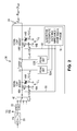
- FIG. 1 depicts a prior art RF system which includes an adaptive impedance matching network.
- the system includes an RF power amplifier PA 20 having an output coupled to the input of a duplexer 22 .
- the duplexer directs the RF signal from amplifier 20 to the system antenna 24 by way of the adaptive impedance matching network 26 .
- Duplexer 22 further channels RF signals received on the antenna to a system receiver (not depicted).
- the adaptive impedance matching network includes a tunable impedance matching network 30 which matches the impedance of the antenna to some target value that matches that of the duplexer.
- an antenna impedance has a real component Rant ranging from 30 to 100 ⁇ and a reactive component j Xant of 0 to +100 j ⁇ .
- the matching network converts the antenna impedance to some target impedance such as an impedance matching that of the coupler 28 .
- the antenna impedance Zant can change, as previously noted, due to a change in the physical environment surrounding the antenna.
- the impedance at the input of the tunable matching network 30 is monitored by periodically measuring the amplitude of the RF voltage at the input and output of the directional coupled 28 using respective peak detectors 32 A and 32 B.
- the phase relationship between the two detected voltages is measured using a phase detector 34 .
- the peak voltage measurements and the phase measurement are then provided to a processing device 36 such as a digital signal processor to compute the impedance.
- the processor adjusts the tunable matching network 30 as needed to return to the target impedance.
- FIG. 1 is a diagram of a prior art RF system which incorporates an adaptive impedance matching network to compensate for changes in an antenna impedance.
- FIG. 2 is a diagram of an RF system which includes an adaptive impedance matching network in accordance with one embodiment of the present invention.
- FIG. 3 is a phasor diagram illustrating part of the operation of the FIG. 2 embodiment and which does not rely upon the use of a phase detector.
- FIGS. 4A-4D are timing diagrams of a simulation further illustrating the operation of the FIG. 2 embodiment.
- FIG. 5 is a diagram of showing an alternative embodiment that uses adjustable attenuator circuitry do reduce the dynamic range requirements of the voltage detectors.
- FIG. 6 is a plot of a complex plane showing the methodology of adjusting the matching network after a change in the antenna impedance is detected.
- FIG. 2 shows an adaptive RF matching network module 38 in accordance with one embodiment of the present invention.
- An RF power amplifier 20 is coupled to a first port of the network module 38 by way of a duplexer 22 followed by an RF switch 40 which switches between various transceiver paths to accommodate various mobile communication standards such as GSM, WCDMA, LTE, etc.
- Another port of the network module 38 is for connecting to an antenna 24 .
- Antenna 24 functions to radiate the RF energy from the amplifier 20 and to receive RF signals which are provided to receiver circuitry by way of the duplexer 22 .
- antenna 24 is a narrow bandwidth miniaturized antenna having a high Q. As a result, the antenna is subject to detuning due to fluctuating body effects and changes in the handset form factor. This detuning has an adverse effect on transmitted radiated power efficiency and over the air receiver sensitivity.
- the adaptive matching network module 38 initially transforms the impedance of the antenna 24 to a target impedance which may be, by way of example, a 50 ⁇ real impedance. Environmental fluctuations may cause the impedance of antenna 24 to change so that the matching network is no longer optimal. As will be described, the adaptive matching network module 38 monitors the impedance of the matched network and, if the impedance varies from the target value, will adjust the matching network so that the impedance is returned to the target value.
- a target impedance which may be, by way of example, a 50 ⁇ real impedance. Environmental fluctuations may cause the impedance of antenna 24 to change so that the matching network is no longer optimal.
- the adaptive matching network module 38 monitors the impedance of the matched network and, if the impedance varies from the target value, will adjust the matching network so that the impedance is returned to the target value.
- the exemplary matching network used in module 38 is a pi type network which includes a series connected inductor Lsense and a pair of shunt connected capacitor arrays C 1 and C 2 disposed on either side of the inductor.
- the capacitor arrays each include an array 44 A and an array 44 B of RF-MEMS (micro-electromechanical system) capacitive switches Cn to C 1 a.
- the capacitive switches are preferably disposed in a binary weighted manner, with there being five capacitive switches connected in parallel, with the relative capacitive values being C, 2 C, 4 C, 8 C and 16 C.
- the five capacitive switches are individually enabled and disabled to provide a total capacitance ranging from C to 31 C in increments of C.
- high voltage switching circuitry (not depicted) is used to control the state of each of the five switches.
- Lsense has a typical inductance of 2 to 8 nano-Henries, with the value of C of the capacitive switches being 0.5 to 4.0 pF.
- Each capacitor bank further includes a small (Co ⁇ 0.125 pF) switched capacitor which is periodically connected in parallel with each of the MEMS capacitive switches 44 A and 44 B. The smaller the value of Co, the greater the voltage detection accuracy required of the RF detectors employed as peak detectors 52 A and 52 B to be described.
- a dither clock present on line 50 is used to control the states of switches 48 A and 48 B which operate to switch capacitors Co in circuit and out of circuit.
- the frequency of the dither clock is determined by the required response time of the RF impedance measurement, which may be as low as a 100 Hz or up to around 1 MHz.
- the dither frequency is not so high as to introduce spikes on the RF sensing lines.
- inductor Lsense In addition to forming part of the impedance matching, inductor Lsense also functions as part of the impedance sensor.
- a pair of peak voltage detectors 52 A and 52 B are connected to detect respective voltages V 1 and V 2 at opposite ends of inductor Lsense. The voltages are periodically sensed when the switched capacitors 46 A and 46 B are connected in circuit by switches 48 A and 48 B and then sensed a second time when the capacitors are switched out of circuit. As will be explained, these four voltage measurements permit the impedance looking into the matching network to be determined. In the event that measured impedance is out of range, the matching network is adjusted by way of capacitor switches 44 A and 44 B to bring the impedance back into range.
- a control block 54 provides various control functions, including the production of the dither clock on line 50 , control of the peak detectors 52 A and 52 B, the computation of the actual network impedance and the re-adjustment of the adaptive matching network to bring the impedance back into range.
- FIG. 2 shows a pair of dither caps 46 A and 46 B having a value CO.
- Dither cap 46 A can be used to determine some useful information regarding the matching network and antenna 24 . However, the following description and analysis is based upon the use of dither cap 46 B alone.
- FIG. 3 is a phasor diagram (not to scale) illustrating the manner in which the four measurements can be used to determine the impedance Z L , which is the impedance looking from the node where V 2 is sampled towards the antenna 24 impedance.
- Impedance Z L can be expresses as follows:
- Voltages V 1 and V 2 are measured using respective peak detectors 52 A and 52 B when switch 48 B is opened based upon the polarity of the dither clock on line 50 so that dither capacitor 46 B (Co) is out of circuit.
- V 1 and V 2 can be plotted on the complex plane showing that the difference between the two voltages is X S which represents the impedance of the sense inductor Lsense.
- the dither clock then closes switch 48 B so that capacitor 46 B is connected in circuit.
- Voltages V 12 and V 22 which correspond to V 1 and V 2 for the previous measurement, are then measured using the respective peak detectors 52 A and 52 B.
- the value of Z L is preferably determined using signal processing circuitry disposed within control unit 54 .
- the phase angle ⁇ is expressed as follows:
- the reactive component X L and real component R L of the impedance Z L can be calculated as follows:
- X L ( X S /2)[( Vr 1 2 ⁇ 1)/( Vr 1 2 +1 ⁇ 2 Vr 1 cos ⁇ ) ⁇ 1] (3)
- R L [X S 2 /( Vr 1 2 +1 ⁇ 2 Vr 1 cos ⁇ ) ⁇ X L 2 ] 1/2 (4)
- the signal processor in the control unit 54 will proceed to alter the matching characteristics in the matching network. As will be described in greater detail, this is carried out by changing the value(s) of capacitors 44 A and 44 B.
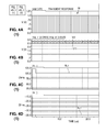
- FIGS. 4A-4D are timing diagrams further illustrating the operation of the subject impedance matching module 38 .
- Waveform 56 of FIG. 4A represents the dither clock which causes the capacitor 46 B (Co) ( FIG. 2 ) to be switched into the matching network and to be switched out of the matching network.
- the two peak detectors 52 A and 52 B sense the peak voltages on opposite sides of inductor Lsense to determine V 1 and V 2 .
- the ratio of V 1 /V 2 , value Vr 1 is then produced. It would also be possible to produce the ratio Vr 1 directly without having to determine the separate values of V 1 and V 2 .
- the peak voltages are sensed to determine the values of V 21 and V 22 .
- the ratio Vr 2 of V 21 /V 22 is then determined.
- the initial impedance Z L1 (which includes the antenna impedance Z ant as one component as previously noted) is as follows:
- the change in antenna impedance could be caused, by way of example, by a change in the antenna environment such as adjusting the manner in which a cell phone is held.
- the change in antenna impedance at time T 1 is rapidly detected as evidenced by a change in the voltage ratios Vr 1 and Vr 2 .
- the control unit 54 then recalculates the new impedance values Z L2 , again using equations (2), (3) and (4), as follows:
- the control unit 54 will then precede to alter the matching network by way of the MEMS 44 A and 44 B so that the matched impedance has returned to the target impedance.
- One approach for adjusting the matching network will now be described. As will be seen, only the change in matching network capacitance to arrive at the target values is needed and not the actual final value of that capacitance.
- the values for R L and X L represent the respective real and imaginary components of the measured impedance. Using these values, the needed change in value of matching network capacitances 44 A and 44 B, the MEMS capacitor arrays, is determine using a signal processor or the like.
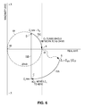
- a chart of the complex impedance plane is shown in FIG. 6 in order to illustrate the manner in which the impedance matching module 38 operates to compensate for changes in the impedance Z ant of antenna 24 .
- the values be in terms of admittance so that values can be simply added together.
- values be in terms of impedance so that they can also be combined by adding.
- the chart of FIG. 6 shows both approaches. When only an imaginary component of an admittance is being changed, the admittance moves along a constant conductance circle, with all of the circles intersecting at the origin 68 .
- the value of C 2 is changed by ⁇ C 2 to provide a new value of Z L , referred to here as Z L new.
- Z L new By adding a parallel reactance, the impedance moves along an arc 72 A of a constant admittance circle from point B to point C.
- the distance and direction of the movement is a function of size of the change ⁇ C 2 and the polarity. In the present example, the polarity is positive (C 2 is to be increased).
- the magnitude of ⁇ C 2 is determined so that point C is at a location in the complex plane such that, when the fixed value inductor Lsense of impedance X S is added in series, the combined, new value of impedance will fall on the constant admittance circle 69 of 20 milli-Siemens. That value at point D is the sum of Z L new plus X S .
- a value of C 1 of the matching network is then produced which provides a reactance X 1 which is of a magnitude sufficient to move the impedance Z L new plus X S to close to a pure resistance of 50 ⁇ as represented by point A. Since the MEMS cap arrays 44 A and 44 B that make up the majority of respective capacitances C 1 and C 2 have only a finite number of possible values, the final impedance value may differ somewhat from the ideal value of 50 ⁇ .
- one approach is to first determine the change in capacitance C 2 to move from point B to point C of FIG. 6 .
- the needed change in reactance ⁇ X 2 can be determined as follows:
- ⁇ X 2 X S [X S X L +R L 2 +X L 2 ⁇ ( R L ( ⁇ X S R L 50 R L 2 +50 X L 2 )) 1/2 ]/[( X L +X S ) 2 +R L ( R L ⁇ 50)] (7)
- X S is the impedance of the inductor Isense
- X L is the measured reactive component of Z L per equation (3)
- R L is the measured resistive component of Z L per equation (4)
- the value 50 is target impedance in ohms.
- ⁇ is the radial frequency 2nf.
- the new value of C 1 needed to shift the full combined impedance (matching network+Zant) from point D back to point A is then determined.
- the equation for calculating the impedance X 1 provided by the new value of C 1 is set forth below. Variables Rn and X n , to be defined later, are used to simplify the following equation for X 1 .
- R n is a variable determined by equation (11) below.
- X n is a variable determined by equation (12) below.
- ⁇ is the radial frequency 2nf.
- R n ( ⁇ X 2 2 R L )/[ R L 2 +( ⁇ X 2 +X L ) 2 ] (11)
- X n X S +[R L 2 ⁇ X 2 +X L 2 ⁇ X 2 +X L ⁇ X 2 2 ]/[ R L 2 +( ⁇ X 2 +X L ) 2 ] (12 )
- X S is the reactance of inductor Lsense
- ⁇ X 2 is the reactance of C 2 per equation (7).
- R L and X L are the real and imaginary parts of Z L per equations (3) and (4).
- MEMS switched capacitors 44 A and 44 B if FIG. 2 could be replaced with voltage controlled capacitances in the form of varactors. In that case, switched capacitors 46 A and 46 B can be eliminated.
- the impedance network changes in response to the dither clock are carried out by altering the magnitude of the varactor control signals in the form of a specific delta voltage to achieve the required difference in capacitance. That change in varactor capacitance can be used as value Xdp in equation (2) above to calculate X L and R L .
- FIG. 5 shows an alternative adaptive matching network module 58 which is similar to that of FIG. 2 in that a pi type architecture is used which includes a series inductor L 1 flanked by a pair of parallel capacitor banks.
- a first one of the capacitor banks includes an array of capacitive MEMS switches 44 A as used in the FIG. 2 embodiment along with three capacitors C A , C B and C C connected in series with one another and in parallel with capacitive switches 44 A.
- the other capacitor bank includes an array of capacitive MEMS switches 44 B as used in the FIG. 2 embodiment and three capacitors C C , C D and C E connected in series with one another and in parallel with capacitive switches 44 B.
- the dither cap (not explicitly depicted) is incorporated into the MEMS capacitive switch 44 B.
- the MEMS switch can selectively connect capacitances C, 2C, 4C, 8C and 16C is parallel.
- the dither cap is switched in and out by switching the control signal to switch 44 B so that the smallest capacitance value C is either in and out of circuit.
- the dither cap 46 B of the FIG. 2 embodiment may be implemented into MEMS capacitor array 44 B and controlled in this same manner.
- each of the peak detectors 52 A and 52 B has an associated sensing node which can be changed in response to the state of switches 60 A and 60 B.
- Peak detectors typically have a limited input range over which they provide an accurate measurement.
- the dynamic range of the ratio V 1 /V 2 which is value Vr 1 of equation (2), can vary over 30 dB for antenna impedances equivalent of VSWRs of up to 8.
- the peak detector 52 A and 52 B sensors can have input dynamic range requirements of 60 dB which can be difficult to achieve.
- FIG. 5 shows one approach for dealing with such a large input voltage dynamic range.
- capacitors C A , C B and C C form a voltage divider, as do capacitors C D , C E and C F .
- corresponding capacitors C A and C D have the same value
- C B and C E each have the same value and capacitors C C and C F . each have the same value.
- respective switches 60 A and 60 B connect nodes 62 B and 64 B as the detector sensing nodes for maximum attenuation.
- nodes 62 A and 64 A are selected for reduced attenuation.
- capacitors C A , C B , C C , C D , C E and C F function together as a pair of adjustable attenuators. Since the attenuators do not include resistances, no loses result.
- the impedance matching networks of FIGS. 2 and 5 are each pi type networks that include three primary impedance components including a series inductance flanked by a pair of parallel capacitances.
- Other types of matching networks can be used, but it is preferred that such networks include at least two primary impedance components (where either similar parallel or similar series components are combined into a primary component) and preferably at least three to provide a sufficiently wide range of impedance matching to cover essentially all possible impedance mismatches.
- a two primary impedance components network would be the three component network of FIG. 2 with capacitances 46 A/ 44 A deleted.
- this matching network does not provide the same matching range as that of FIG. 2 , it is very useful in those instances where a wide range of matching is not needed while still providing an impedance detection capability.
- the RF detectors are implemented in both the FIG. 2 and FIG. 5 embodiments in the form of peak detectors 52 A and 52 B. However, rather than using peak detectors it would be possible to use any other types of detectors including RMS, linear and logarithmic.
Landscapes
- Measurement Of Resistance Or Impedance (AREA)
- Transmitters (AREA)
- Input Circuits Of Receivers And Coupling Of Receivers And Audio Equipment (AREA)
Abstract
Description
- 1. Field of the Invention
- The present invention relates generally to RF impedance measurement and in particular to RF impedance measurements using two point voltage sampling without a phase detector. Some embodiments also relate to adjusting an impedance matching network after the measurement.
- 2. Description of Related Art
- Mobile handsets such as cellular phones are being manufactured using higher levels of integration and use in broader frequency band coverage. As a result, the performance limits of embedded antenna technology are being stretched. Variations in load impedance at the antenna due to environmental changes such as the position at which the phone is held, the frequency band being used and other contributors create a mismatch or increased voltage standing wave ratio (VSWR) at the antenna port. In addition, the body effects of a head or hand near the antenna contribute to capacitive loading which also results in an impedance mismatch. This can lead to a shift in antenna center frequency and an increased VSWR mismatch. In addition to reception problems, any mismatch will further result in a reduction in power radiated from the antenna.
-
FIG. 1 depicts a prior art RF system which includes an adaptive impedance matching network. The system includes an RFpower amplifier PA 20 having an output coupled to the input of aduplexer 22. The duplexer directs the RF signal fromamplifier 20 to thesystem antenna 24 by way of the adaptive impedance matchingnetwork 26.Duplexer 22 further channels RF signals received on the antenna to a system receiver (not depicted). The adaptive impedance matching network includes a tunable impedance matchingnetwork 30 which matches the impedance of the antenna to some target value that matches that of the duplexer. Typically, an antenna impedance has a real component Rant ranging from 30 to 100Ω and a reactive component j Xant of 0 to +100 jΩ. The matching network converts the antenna impedance to some target impedance such as an impedance matching that of thecoupler 28. - The antenna impedance Zant can change, as previously noted, due to a change in the physical environment surrounding the antenna. The impedance at the input of the
tunable matching network 30 is monitored by periodically measuring the amplitude of the RF voltage at the input and output of the directional coupled 28 usingrespective peak detectors phase detector 34. The peak voltage measurements and the phase measurement are then provided to aprocessing device 36 such as a digital signal processor to compute the impedance. In the event the measured impedance differs from the target impedance due to a change, by way of example, in the antenna characteristics, the processor adjusts thetunable matching network 30 as needed to return to the target impedance. - The above-described approach requires an impedance sensing section which is separate from the impedance matching section. In addition, a phase detector is used. A phase detector having good accuracy and low current is difficult to achieve over the 690 Mhz to 2690 Mhz range of interest in many cell phone applications. As will become apparent to those skilled in the art upon a reading of the following Detailed Description of the Invention together with the drawings, an RF impedance improved detection scheme is disclosed which does not rely upon a phase detector and which does not require a sensing element separate from the matching network.
-
FIG. 1 is a diagram of a prior art RF system which incorporates an adaptive impedance matching network to compensate for changes in an antenna impedance. -
FIG. 2 is a diagram of an RF system which includes an adaptive impedance matching network in accordance with one embodiment of the present invention. -
FIG. 3 is a phasor diagram illustrating part of the operation of theFIG. 2 embodiment and which does not rely upon the use of a phase detector. -
FIGS. 4A-4D are timing diagrams of a simulation further illustrating the operation of theFIG. 2 embodiment. -
FIG. 5 is a diagram of showing an alternative embodiment that uses adjustable attenuator circuitry do reduce the dynamic range requirements of the voltage detectors. -
FIG. 6 is a plot of a complex plane showing the methodology of adjusting the matching network after a change in the antenna impedance is detected. - Referring again to the drawings,
FIG. 2 shows an adaptive RFmatching network module 38 in accordance with one embodiment of the present invention. AnRF power amplifier 20 is coupled to a first port of thenetwork module 38 by way of aduplexer 22 followed by anRF switch 40 which switches between various transceiver paths to accommodate various mobile communication standards such as GSM, WCDMA, LTE, etc. Another port of thenetwork module 38 is for connecting to anantenna 24.Antenna 24 functions to radiate the RF energy from theamplifier 20 and to receive RF signals which are provided to receiver circuitry by way of theduplexer 22. In many applications such as cellular phones,antenna 24 is a narrow bandwidth miniaturized antenna having a high Q. As a result, the antenna is subject to detuning due to fluctuating body effects and changes in the handset form factor. This detuning has an adverse effect on transmitted radiated power efficiency and over the air receiver sensitivity. - The adaptive
matching network module 38 initially transforms the impedance of theantenna 24 to a target impedance which may be, by way of example, a 50Ω real impedance. Environmental fluctuations may cause the impedance ofantenna 24 to change so that the matching network is no longer optimal. As will be described, the adaptivematching network module 38 monitors the impedance of the matched network and, if the impedance varies from the target value, will adjust the matching network so that the impedance is returned to the target value. - The exemplary matching network used in
module 38 is a pi type network which includes a series connected inductor Lsense and a pair of shunt connected capacitor arrays C1 and C2 disposed on either side of the inductor. The capacitor arrays each include anarray 44A and anarray 44B of RF-MEMS (micro-electromechanical system) capacitive switches Cn to C1 a. The capacitive switches are preferably disposed in a binary weighted manner, with there being five capacitive switches connected in parallel, with the relative capacitive values being C, 2 C, 4 C, 8 C and 16 C. The five capacitive switches are individually enabled and disabled to provide a total capacitance ranging from C to 31 C in increments of C. As is well known, high voltage switching circuitry (not depicted) is used to control the state of each of the five switches. Lsense has a typical inductance of 2 to 8 nano-Henries, with the value of C of the capacitive switches being 0.5 to 4.0 pF. Each capacitor bank further includes a small (Co<0.125 pF) switched capacitor which is periodically connected in parallel with each of the MEMScapacitive switches peak detectors line 50 is used to control the states ofswitches - In addition to forming part of the impedance matching, inductor Lsense also functions as part of the impedance sensor. A pair of
peak voltage detectors capacitors switches capacitor switches control block 54 provides various control functions, including the production of the dither clock online 50, control of thepeak detectors - Note that
FIG. 2 shows a pair ofdither caps cap 46A can be used to determine some useful information regarding the matching network andantenna 24. However, the following description and analysis is based upon the use ofdither cap 46B alone. -
FIG. 3 is a phasor diagram (not to scale) illustrating the manner in which the four measurements can be used to determine the impedance ZL, which is the impedance looking from the node where V2 is sampled towards theantenna 24 impedance. Thus, ZL is the parallel combination of the matching network output capacitance C2 (sum ofparallel capacitors -
Z L =R L +jX L (1) - Voltages V1 and V2 are measured using
respective peak detectors switch 48B is opened based upon the polarity of the dither clock online 50 so thatdither capacitor 46B (Co) is out of circuit. Thus, it can be seen from theFIG. 3 diagram where V1 and V2 can be plotted on the complex plane showing that the difference between the two voltages is XS which represents the impedance of the sense inductor Lsense. After the first measurements are made, the dither clock then closesswitch 48B so thatcapacitor 46B is connected in circuit. Voltages V12 and V22, which correspond to V1 and V2 for the previous measurement, are then measured using therespective peak detectors capacitor 46B. Inspection of theFIG. 3 diagram indicates that the values RL and XL of the impedance ZL (which includes the antenna impedance Zant as one component) can then be ascertained without the use of a phase detector. - The value of ZL is preferably determined using signal processing circuitry disposed within
control unit 54. The phase angle φ is expressed as follows: -
Cos φ=−0.5[Xdp 2(Vr12 −Vr22)+X S 2]/(X S *Xdp*Vr1) (2) - where,
-
- Vr1 is the ratio of V1/V2;
- Vr2 is the ratio of V12/V22;
- Xdp is the impedance of the
dither cap 46B; and - XS is the impedance of inductor Lsense.
- Once the phase angle is known, the reactive component XL and real component RL of the impedance ZL can be calculated as follows:
-
X L=(X S/2)[(Vr12−1)/(Vr12+1−2Vr1 cos φ)−1] (3) -
and -
R L =[X S 2/(Vr12+1−2Vr1 cos φ)−X L 2]1/2 (4) - Assuming that the value of ZL has moved away from the target value because, for example, of changes in the antenna environment, the signal processor in the
control unit 54 will proceed to alter the matching characteristics in the matching network. As will be described in greater detail, this is carried out by changing the value(s) ofcapacitors -
FIGS. 4A-4D are timing diagrams further illustrating the operation of the subjectimpedance matching module 38.Waveform 56 ofFIG. 4A represents the dither clock which causes thecapacitor 46B (Co) (FIG. 2 ) to be switched into the matching network and to be switched out of the matching network. As previously described, when capacitor Co is present in the network, the twopeak detectors - A change in the antenna load impedance is simulated in the timing diagrams at a time T1=25 μs. Prior to that time, it can be seen from
FIG. 4B that the ratio Vr1 is approximately 2.6 and the ratio Vr2 is approximately 2.8. The two ratios are then processed per equations (2), (3) and (4) bycontrol unit 54 to produce a real component RL1 and an imaginary component XL1 of the impedance RL. In this example, the initial impedance ZL1 (which includes the antenna impedance Zant as one component as previously noted) is as follows: -
Z L1 =R L1 +jX L1=100−j35.4 Ω (5) - The change in antenna impedance could be caused, by way of example, by a change in the antenna environment such as adjusting the manner in which a cell phone is held. As can be seen in
FIG. 4B , the change in antenna impedance at time T1 is rapidly detected as evidenced by a change in the voltage ratios Vr1 and Vr2. Vr1 changed from about 2.6 to 2.5 and Vr2 changed from about 2.8. Thecontrol unit 54 then recalculates the new impedance values ZL2, again using equations (2), (3) and (4), as follows: -
Z L2 =R L2 +jX L2=50−j17.7 Ω (6) - If it is assumed that the target impedance is reflected by equation (5) above, the
control unit 54 will then precede to alter the matching network by way of theMEMS - As was previously shown by equations (3) and (4), the values for RL and XL represent the respective real and imaginary components of the measured impedance. Using these values, the needed change in value of matching
network capacitances FIG. 6 in order to illustrate the manner in which theimpedance matching module 38 operates to compensate for changes in the impedance Zant ofantenna 24. In order to combine parallel components, it is preferred that the values be in terms of admittance so that values can be simply added together. Similarly, for series components, it is preferred that values be in terms of impedance so that they can also be combined by adding. The chart ofFIG. 6 shows both approaches. When only an imaginary component of an admittance is being changed, the admittance moves along a constant conductance circle, with all of the circles intersecting at theorigin 68. - Initially, assume that that the matching network is at the optimum value to transform the present antenna impedance Zant to the optimum value in this example of in this example of 50+j0Ω purely real resistance. This condition is represented on the
FIG. 6 chart at point A. As can be seen, point A lies of the real axis at the 50Ω point which falls on a constant conductance circle of 20 milli Siemens. If the antenna impedance Zant is changed due to changes in the antenna environment for example, the antenna impedance Zant will change. The impedance measured by thematching network module 38 is actually ZL, the parallel combination of Zant and impedance ZC2 of capacitor C2 of the matching network. Thus, when Zant changes so does ZL, as indicated by the transition from point A to point B of theFIG. 6 chart. - In order to return the altered impedance to the target impedance at point A, it is usually necessary to adjust both the value of capacitances C1 and C2 of the matching network. First, the value of C2 is changed by ΔC2 to provide a new value of ZL, referred to here as ZLnew. By adding a parallel reactance, the impedance moves along an
arc 72A of a constant admittance circle from point B to point C. The distance and direction of the movement is a function of size of the change ΔC2 and the polarity. In the present example, the polarity is positive (C2 is to be increased). The magnitude of ΔC2 is determined so that point C is at a location in the complex plane such that, when the fixed value inductor Lsense of impedance XS is added in series, the combined, new value of impedance will fall on theconstant admittance circle 69 of 20 milli-Siemens. That value at point D is the sum of ZLnew plus XS. At this point, a value of C1 of the matching network is then produced which provides a reactance X1 which is of a magnitude sufficient to move the impedance ZLnew plus XS to close to a pure resistance of 50Ω as represented by point A. Since theMEMS cap arrays - In order to carry out the above transformation, one approach is to first determine the change in capacitance C2 to move from point B to point C of
FIG. 6 . The needed change in reactance ΔX2 can be determined as follows: -
ΔX 2 =X S [X S X L +R L 2 +X L 2−(R L(−X S R L50R L 2+50X L 2))1/2]/[(X L +X S)2 +R L(R L−50)] (7) - where
- XS is the impedance of the inductor Isense;
- XL is the measured reactive component of ZL per equation (3);
- RL is the measured resistive component of ZL per equation (4); and
- the
value 50 is target impedance in ohms. - Thus, the needed change to the present value of C2 in order to move from point B to point C of
FIG. 6 is as follows: -
ΔC 2−1/(ωΔX 2) (8) - where ω is the radial frequency 2nf.
- The new value of C1 needed to shift the full combined impedance (matching network+Zant) from point D back to point A is then determined. The equation for calculating the impedance X1 provided by the new value of C1 is set forth below. Variables Rn and Xn, to be defined later, are used to simplify the following equation for X1.
-
X 1=5[10X n+(−100R n 2+2R n X n 2+2R n 3)1/2]/(R n −50) (9) - where,
- Rn is a variable determined by equation (11) below; and
- Xn is a variable determined by equation (12) below.
- The new value of C1 is then as follows:
-
C 1=−1/(ωX 1) (10) - where ω is the radial frequency 2nf.
- The values of variables Rn and Xn used in equation (9) are as follows:
-
R n=(ΔX 2 2 R L)/[R L 2+(ΔX 2 +X L)2] (11) -
and -
X n =X S +[R L 2 ΔX 2 +X L 2 ΔX 2 +X L ΔX 2 2]/[R L 2+(ΔX 2 +X L)2] (12 ) - where
- XS is the reactance of inductor Lsense;
- ΔX2 is the reactance of C2 per equation (7); and
- RL and XL are the real and imaginary parts of ZL per equations (3) and (4).
- Thus, once the new value of C1 of the matching network has been provided per equation (10), the impedance looking into the matching network on the C1 side will have returned to point A of
FIG. 6 which is at or near a pure resistance of 50Ω. Thus, once the actual values of C1 and C2 in theFIG. 2 impedance matching network have been updated, the impedance matching sequence is completed. - Note that MEMS switched
capacitors FIG. 2 could be replaced with voltage controlled capacitances in the form of varactors. In that case, switchedcapacitors -
FIG. 5 shows an alternative adaptivematching network module 58 which is similar to that ofFIG. 2 in that a pi type architecture is used which includes a series inductor L1 flanked by a pair of parallel capacitor banks. A first one of the capacitor banks includes an array of capacitive MEMS switches 44A as used in theFIG. 2 embodiment along with three capacitors CA, CB and CC connected in series with one another and in parallel withcapacitive switches 44A. The other capacitor bank includes an array of capacitive MEMS switches 44B as used in theFIG. 2 embodiment and three capacitors CC, CD and CE connected in series with one another and in parallel withcapacitive switches 44B. In this embodiment, the dither cap (not explicitly depicted) is incorporated into theMEMS capacitive switch 44B. As previously noted, the MEMS switch can selectively connect capacitances C, 2C, 4C, 8C and 16C is parallel. The dither cap is switched in and out by switching the control signal to switch 44B so that the smallest capacitance value C is either in and out of circuit. Note that thedither cap 46B of theFIG. 2 embodiment may be implemented intoMEMS capacitor array 44B and controlled in this same manner. - As can be seen in
FIG. 5 , each of thepeak detectors switches peak detector -
FIG. 5 shows one approach for dealing with such a large input voltage dynamic range. Relatively small value capacitors CA, CB and CC form a voltage divider, as do capacitors CD, CE and CF. Preferably corresponding capacitors CA and CD have the same value, and CB and CE each have the same value and capacitors CC and CF. each have the same value. For relatively strong RF signals at the matching network, as determined by anRF detector 65,respective switches nodes nodes - As previously noted, the impedance matching networks of
FIGS. 2 and 5 are each pi type networks that include three primary impedance components including a series inductance flanked by a pair of parallel capacitances. Other types of matching networks can be used, but it is preferred that such networks include at least two primary impedance components (where either similar parallel or similar series components are combined into a primary component) and preferably at least three to provide a sufficiently wide range of impedance matching to cover essentially all possible impedance mismatches. On example of a two primary impedance components network would be the three component network ofFIG. 2 withcapacitances 46A/44A deleted. Although this matching network does not provide the same matching range as that ofFIG. 2 , it is very useful in those instances where a wide range of matching is not needed while still providing an impedance detection capability. - The RF detectors are implemented in both the
FIG. 2 andFIG. 5 embodiments in the form ofpeak detectors - Thus, various embodiments of an adaptive impedance network and associated circuitry have been disclosed. Although these embodiments have been described in some detail, certain changes can be made by those skilled in the art without departing from the spirit and scope of the present invention as defined by the appended claims.
Claims (23)
Priority Applications (4)
| Application Number | Priority Date | Filing Date | Title |
|---|---|---|---|
| US13/065,881 US8674782B2 (en) | 2011-03-31 | 2011-03-31 | RF impedance detection using two point voltage sampling |
| PCT/US2012/031891 WO2012135853A2 (en) | 2011-03-31 | 2012-04-02 | Rf impedance detection using two point voltage sampling |
| JP2014502698A JP6342798B2 (en) | 2011-03-31 | 2012-04-02 | RF impedance detection using two-point voltage sampling |
| JP2018029847A JP6607982B2 (en) | 2011-03-31 | 2018-02-22 | RF impedance detection using two-point voltage sampling |
Applications Claiming Priority (1)
| Application Number | Priority Date | Filing Date | Title |
|---|---|---|---|
| US13/065,881 US8674782B2 (en) | 2011-03-31 | 2011-03-31 | RF impedance detection using two point voltage sampling |
Publications (2)
| Publication Number | Publication Date |
|---|---|
| US20120249259A1 true US20120249259A1 (en) | 2012-10-04 |
| US8674782B2 US8674782B2 (en) | 2014-03-18 |
Family
ID=46926435
Family Applications (1)
| Application Number | Title | Priority Date | Filing Date |
|---|---|---|---|
| US13/065,881 Active 2032-09-03 US8674782B2 (en) | 2011-03-31 | 2011-03-31 | RF impedance detection using two point voltage sampling |
Country Status (3)
| Country | Link |
|---|---|
| US (1) | US8674782B2 (en) |
| JP (2) | JP6342798B2 (en) |
| WO (1) | WO2012135853A2 (en) |
Cited By (12)
| Publication number | Priority date | Publication date | Assignee | Title |
|---|---|---|---|---|
| US20120007692A1 (en) * | 2010-07-06 | 2012-01-12 | Lg Innotek Co., Ltd. | Impedance matching apparatus and method of antenna circuit |
| US20130324057A1 (en) * | 2012-05-31 | 2013-12-05 | Qualcomm Incorporated | Determining a delivered power estimate and a load impedance estimate using a directional coupler |
| US20140210551A1 (en) * | 2011-04-18 | 2014-07-31 | Advanced Energy Industries, Inc. | Variable-class amplifier, system, and method |
| EP3337043A1 (en) * | 2016-12-16 | 2018-06-20 | Intel IP Corporation | Control circuit and apparatus, radio frequency circuit and apparatus, transceiver, mobile terminal, methods and computer programs for determining calibration values for a radio frequency circuit |
| CN110048685A (en) * | 2019-02-22 | 2019-07-23 | 苏州加士革电子科技有限公司 | For ClassE2The motional impedance regulating system of DC-DC converter |
| EP3767829A1 (en) * | 2019-07-16 | 2021-01-20 | Technische Universität Dresden | Assembly for automatic impedance adjustment |
| US11121693B1 (en) * | 2020-01-16 | 2021-09-14 | Amazon Technologies, Inc. | Radio frequency port impedance detection using concurrent radios |
| US11201595B2 (en) * | 2015-11-24 | 2021-12-14 | Skyworks Solutions, Inc. | Cascode power amplifier with switchable output matching network |
| EP3933416A1 (en) * | 2020-06-30 | 2022-01-05 | Imec VZW | Rf impedance measurement circuit |
| CN116418309A (en) * | 2021-12-29 | 2023-07-11 | 上海微创惟美医疗科技(集团)有限公司 | Impedance matching method of impedance matching circuit |
| CN118981997A (en) * | 2024-08-15 | 2024-11-19 | 江苏神州半导体科技有限公司 | An impedance adaptive matching method for radio frequency power supply |
| WO2025064113A1 (en) * | 2023-09-19 | 2025-03-27 | Qualcomm Incorporated | Full duplex transceiver with impedance sensing |
Families Citing this family (6)
| Publication number | Priority date | Publication date | Assignee | Title |
|---|---|---|---|---|
| US9667216B2 (en) * | 2015-08-12 | 2017-05-30 | Shure Acquisition Holdings, Inc. | Wideband tunable combiner system |
| US10700658B2 (en) * | 2016-02-19 | 2020-06-30 | Psemi Corporation | Adaptive tuning networks with direct mapped multiple channel filter tuning |
| JP6609021B1 (en) * | 2018-11-12 | 2019-11-20 | 株式会社ジーエスエレテック | Impedance matching circuit and non-contact power feeding system having the impedance matching circuit |
| JP7275624B2 (en) * | 2019-02-13 | 2023-05-18 | 株式会社デンソー | Frequency band variable high frequency amplifier |
| JP7234177B2 (en) | 2020-03-17 | 2023-03-07 | 株式会社東芝 | semiconductor equipment |
| KR20230007199A (en) * | 2021-07-05 | 2023-01-12 | 삼성전자주식회사 | Antenna matching circuit |
Family Cites Families (17)
| Publication number | Priority date | Publication date | Assignee | Title |
|---|---|---|---|---|
| JPS53131736A (en) * | 1977-04-21 | 1978-11-16 | Kokusai Electric Co Ltd | Method of automatically tuning and matching antenna |
| JPS60264126A (en) * | 1984-06-13 | 1985-12-27 | Teru Saamuko Kk | Automatic tuning circuit in plasma equipment |
| JP3176128B2 (en) * | 1992-06-25 | 2001-06-11 | 株式会社ダイヘン | Output voltage measuring device for impedance matching device |
| JPH11251928A (en) * | 1998-02-26 | 1999-09-17 | Nec Eng Ltd | Automatic antenna matching circuit and method |
| KR100358444B1 (en) | 1999-07-27 | 2002-10-25 | 엘지전자 주식회사 | Antenna Matching Apparatus of Portable Radio Telephone |
| JP4421062B2 (en) * | 1999-10-22 | 2010-02-24 | 株式会社エヌエフ回路設計ブロック | Impedance measurement method and apparatus |
| JP2002139528A (en) * | 2000-11-01 | 2002-05-17 | Nf Corp | Impedance measuring device |
| US6608603B2 (en) | 2001-08-24 | 2003-08-19 | Broadcom Corporation | Active impedance matching in communications systems |
| JP4469632B2 (en) * | 2004-02-24 | 2010-05-26 | 富士通株式会社 | Control device for antenna matching circuit |
| JP4987723B2 (en) * | 2004-11-19 | 2012-07-25 | エプコス アクチエンゲゼルシャフト | Device with a coupled load line at the output of the amplifier stage |
| JP2007003407A (en) * | 2005-06-24 | 2007-01-11 | Nf Corp | Method and apparatus for measuring impedance |
| WO2008007330A2 (en) * | 2006-07-12 | 2008-01-17 | Nxp B.V. | Load-line adaptation |
| US7535312B2 (en) * | 2006-11-08 | 2009-05-19 | Paratek Microwave, Inc. | Adaptive impedance matching apparatus, system and method with improved dynamic range |
| US8213885B2 (en) | 2008-04-11 | 2012-07-03 | Nautel Limited | Impedance measurement in an active radio frequency transmitter |
| JP5167053B2 (en) * | 2008-09-30 | 2013-03-21 | 吉川アールエフシステム株式会社 | Automatic matching method and automatic matching circuit |
| DE102009024747A1 (en) | 2009-01-22 | 2010-07-29 | Epcos Ag | Adaptive impedance matching circuit and adaptation method for duplexing standards |
| US8963611B2 (en) * | 2009-06-19 | 2015-02-24 | Qualcomm Incorporated | Power and impedance measurement circuits for a wireless communication device |
-
2011
- 2011-03-31 US US13/065,881 patent/US8674782B2/en active Active
-
2012
- 2012-04-02 WO PCT/US2012/031891 patent/WO2012135853A2/en not_active Ceased
- 2012-04-02 JP JP2014502698A patent/JP6342798B2/en active Active
-
2018
- 2018-02-22 JP JP2018029847A patent/JP6607982B2/en active Active
Cited By (17)
| Publication number | Priority date | Publication date | Assignee | Title |
|---|---|---|---|---|
| US20120007692A1 (en) * | 2010-07-06 | 2012-01-12 | Lg Innotek Co., Ltd. | Impedance matching apparatus and method of antenna circuit |
| US8928430B2 (en) * | 2010-07-06 | 2015-01-06 | Lg Innotek Co., Ltd. | Impedance matching apparatus and method of antenna circuit |
| US20140210551A1 (en) * | 2011-04-18 | 2014-07-31 | Advanced Energy Industries, Inc. | Variable-class amplifier, system, and method |
| US9225299B2 (en) * | 2011-04-18 | 2015-12-29 | Advanced Energy Industries, Inc. | Variable-class amplifier, system, and method |
| US20130324057A1 (en) * | 2012-05-31 | 2013-12-05 | Qualcomm Incorporated | Determining a delivered power estimate and a load impedance estimate using a directional coupler |
| US11201595B2 (en) * | 2015-11-24 | 2021-12-14 | Skyworks Solutions, Inc. | Cascode power amplifier with switchable output matching network |
| US10938425B2 (en) | 2016-12-16 | 2021-03-02 | Intel IP Corporation | Control circuit and apparatus, radio frequency circuit and apparatus, transceiver, mobile terminal, methods and computer programs for determining calibration values for a radio frequency circuit |
| EP3337043A1 (en) * | 2016-12-16 | 2018-06-20 | Intel IP Corporation | Control circuit and apparatus, radio frequency circuit and apparatus, transceiver, mobile terminal, methods and computer programs for determining calibration values for a radio frequency circuit |
| CN110048685A (en) * | 2019-02-22 | 2019-07-23 | 苏州加士革电子科技有限公司 | For ClassE2The motional impedance regulating system of DC-DC converter |
| EP3767829A1 (en) * | 2019-07-16 | 2021-01-20 | Technische Universität Dresden | Assembly for automatic impedance adjustment |
| US11121693B1 (en) * | 2020-01-16 | 2021-09-14 | Amazon Technologies, Inc. | Radio frequency port impedance detection using concurrent radios |
| US11658634B1 (en) | 2020-01-16 | 2023-05-23 | Amazon Technologies, Inc. | Radio frequency port impedance detection using concurrent radios |
| EP3933416A1 (en) * | 2020-06-30 | 2022-01-05 | Imec VZW | Rf impedance measurement circuit |
| US11601109B2 (en) | 2020-06-30 | 2023-03-07 | IM EC vzw | RF impedance measurement circuit |
| CN116418309A (en) * | 2021-12-29 | 2023-07-11 | 上海微创惟美医疗科技(集团)有限公司 | Impedance matching method of impedance matching circuit |
| WO2025064113A1 (en) * | 2023-09-19 | 2025-03-27 | Qualcomm Incorporated | Full duplex transceiver with impedance sensing |
| CN118981997A (en) * | 2024-08-15 | 2024-11-19 | 江苏神州半导体科技有限公司 | An impedance adaptive matching method for radio frequency power supply |
Also Published As
| Publication number | Publication date |
|---|---|
| JP2018129810A (en) | 2018-08-16 |
| JP2014518026A (en) | 2014-07-24 |
| WO2012135853A3 (en) | 2012-12-27 |
| US8674782B2 (en) | 2014-03-18 |
| WO2012135853A2 (en) | 2012-10-04 |
| JP6607982B2 (en) | 2019-11-20 |
| JP6342798B2 (en) | 2018-06-13 |
Similar Documents
| Publication | Publication Date | Title |
|---|---|---|
| US8674782B2 (en) | RF impedance detection using two point voltage sampling | |
| KR101645119B1 (en) | System and method for a directional coupler | |
| EP1915819B1 (en) | Integrated load impedance sensing for tunable matching networks | |
| KR101855836B1 (en) | System and method for a directional coupler | |
| EP2660987B1 (en) | Device and method for antenna impedance matching | |
| US8095085B2 (en) | Automatic antenna tuning unit for software-defined and cognitive radio | |
| KR101944592B1 (en) | Voltage standing wave ratio measurement and tuning systems and methods | |
| US8565695B2 (en) | Detection of the value of an impedance of a radiofrequency system | |
| US9698758B2 (en) | Methods for tuning an adaptive impedance matching network with a look-up table | |
| Ida et al. | An adaptive impedance matching system and its application to mobile antennas | |
| CN115803639B (en) | Power detector | |
| US7598805B2 (en) | Load insensitive balanced power amplifier and related operating method | |
| Firrao et al. | An automatic antenna tuning system using only RF signal amplitudes | |
| EP1792192A1 (en) | Circuit for detecting the impedance of a load | |
| EP2689257A2 (en) | Simple and minimally invasive methods and systems for sensing and computing load impedance | |
| Zhang et al. | 26.4 a reflection-coefficient sensor for 28ghz beamforming transmitters in 22nm fd-soi cmos | |
| WO2016034893A1 (en) | Tuning reconfigurable multi-port antennas | |
| KR101694548B1 (en) | Impedance tracer in adaptive tuning antenna circuit | |
| Gonçalves et al. | A compact impedance measurement solution for systems operating in load varying scenarios | |
| KR20250102960A (en) | Phase discriminator for reflected waves and operating method thereof | |
| JPH04350573A (en) | Impedance measuring apparatus | |
| Ida et al. | An adaptive impedance matching system for mobile antennas | |
| Rogers | Model fitting functions |
Legal Events
| Date | Code | Title | Description |
|---|---|---|---|
| AS | Assignment |
Owner name: TEXAS INSTRUMENTS INCORPORATED, TEXAS Free format text: ASSIGNMENT OF ASSIGNORS INTEREST;ASSIGNORS:KEESE, WILLIAM O.;RADOVANOVIC, SASA;SIMON, DANIEL L.;SIGNING DATES FROM 20120221 TO 20120222;REEL/FRAME:027903/0123 |
|
| STCF | Information on status: patent grant |
Free format text: PATENTED CASE |
|
| MAFP | Maintenance fee payment |
Free format text: PAYMENT OF MAINTENANCE FEE, 4TH YEAR, LARGE ENTITY (ORIGINAL EVENT CODE: M1551) Year of fee payment: 4 |
|
| MAFP | Maintenance fee payment |
Free format text: PAYMENT OF MAINTENANCE FEE, 8TH YEAR, LARGE ENTITY (ORIGINAL EVENT CODE: M1552); ENTITY STATUS OF PATENT OWNER: LARGE ENTITY Year of fee payment: 8 |
|
| MAFP | Maintenance fee payment |
Free format text: PAYMENT OF MAINTENANCE FEE, 12TH YEAR, LARGE ENTITY (ORIGINAL EVENT CODE: M1553); ENTITY STATUS OF PATENT OWNER: LARGE ENTITY Year of fee payment: 12 |