US20120249178A1 - Monitoring method for three-dimensional intergrated circuit (3d ic) and apparatus using the same - Google Patents
Monitoring method for three-dimensional intergrated circuit (3d ic) and apparatus using the same Download PDFInfo
- Publication number
- US20120249178A1 US20120249178A1 US13/493,976 US201213493976A US2012249178A1 US 20120249178 A1 US20120249178 A1 US 20120249178A1 US 201213493976 A US201213493976 A US 201213493976A US 2012249178 A1 US2012249178 A1 US 2012249178A1
- Authority
- US
- United States
- Prior art keywords
- tsvs
- inverters
- output signal
- tsv
- monitoring apparatus
- Prior art date
- Legal status (The legal status is an assumption and is not a legal conclusion. Google has not performed a legal analysis and makes no representation as to the accuracy of the status listed.)
- Granted
Links
Images


Classifications
-
- H—ELECTRICITY
- H10—SEMICONDUCTOR DEVICES; ELECTRIC SOLID-STATE DEVICES NOT OTHERWISE PROVIDED FOR
- H10P—GENERIC PROCESSES OR APPARATUS FOR THE MANUFACTURE OR TREATMENT OF DEVICES COVERED BY CLASS H10
- H10P74/00—Testing or measuring during manufacture or treatment of wafers, substrates or devices
- H10P74/27—Structural arrangements therefor
- H10P74/277—Circuits for electrically characterising or monitoring manufacturing processes, e.g. circuits in tested chips or circuits in testing wafers
Definitions
- the present disclosure relates to a monitoring method for a three dimensional integrated circuit (3D IC), and in particular relates to a monitoring method for Through Silicon Vias (TSVs) of 3D ICs and apparatus using the same.
- 3D IC three dimensional integrated circuit
- TSVs Through Silicon Vias
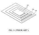
- FIG. 1 shows an outside view diagram of stacked ICs in the prior art.
- the ICs 102 are connected with the lead frame 106 via the leads 104 .
- MOSFET metal oxide semiconductor field effect transistor
- RC delay occurs, due to the smaller dimensions of the leads 104 ; which seriously effects performance of the deep submicron MOSFETs.
- 3D ICs three dimensional integrated circuits
- FIG. 2A shows an outside view diagram of a 3D IC.
- the 3D IC 200 comprises a plurality of ICs 202 .
- the ICs 202 are stacked in the 3D space to shorten the total wire length to reduce RC delay.
- FIG. 2B shows an inside structure diagram of the 3D IC.
- Through-Silicon Vias (TSVs) are disposed throughout, connecting the plurality of ICs 202 therein. Fabrication of TSVs is critical for performance of deep submicron ICs.
- TSV manufacturing pilot holes of a certain dimension are fabricated on the IC 202 and then filled with a suitable conducting material. However, there is no efficient method to determine whether the TSVs meet manufacturing standards. Therefore, a simple and efficient monitoring method for Through Silicon Vias (TSVs) of 3D ICs is called for.
- TSVs Through Silicon Vias
- the monitoring method includes: providing a plurality of TSVs, providing a plurality of inverters; connecting the inverters with the TSVs in series as a circuit loop; enabling the circuit loop to oscillate; measuring an output signal on an output end of one of the plurality of inverters; and determining the manufacturing state of the plurality of TSVs of the 3D IC based on the output signal.
- the monitoring apparatus includes a plurality of TSVs, a plurality of inverters, wherein the plurality of inverters and the TSVs are connected in series as a circuit loop; a signal controller for enabling the circuit loop to oscillate; and a signal processor for measuring an output signal on an output end of one of the plurality of inverters and determining the manufacturing state of the plurality of TSVs of the 3D IC based on the output signal.
- FIG. 1 shows an outside view diagram of stacked ICs in the prior art
- FIG. 2A shows an outside view diagram of a 3D IC
- FIG. 2B shows an inside structure diagram of the 3D IC
- FIG. 3 shows a cross-section diagram of TSVs
- FIG. 4 is a schematic diagram of a monitoring apparatus for the TSV of the 3D IC according to one exemplary embodiment
- FIG. 5 is a schematic diagram illustrating how an inverter works
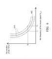
- FIG. 6 shows the relationship diagram between the frequency of the output signal and the number of TSVs
- FIG. 7 is a schematic diagram of a monitoring apparatus for the TSV of the 3D IC according to another exemplary embodiments.
- FIG. 8A and FIG. 8B is a schematic diagram of a monitoring apparatus for the TSV of the 3D IC according to the other exemplary embodiments;
- FIG. 9 is a schematic diagram wherein the inverters are disposed in different wafers according to the exemplary embodiment.
- FIG. 10 is a flow chart of the monitoring method for the TSVs of the 3D IC.
- FIG. 3 shows a cross-section diagram of Through-Silicon Vias (TSVs).
- TSVs Through-Silicon Vias
- WAT Wafer Acceptance Test
- Manufacturing of a 3D IC includes, creating pilot holes on the ICs 202 , whereby the holes are filled with conductive material to form the TSVs 220 , and surrounded with insulating layers 302 .
- the TSVs 220 and insulating layers 302 may be regarded as a RLC equivalent load composed of an equivalent resistor R, an equivalent inductor L and an equivalent capacitor C.
- the RLC equivalent value of the TSVs 220 varies.
- the RLC equivalent value of the TSVs 220 may also vary. Therefore, one of the methods of the embodiment is to inspect the manufacturing state of the TSVs 220 with an optimum state.
- FIG. 4 is a schematic diagram of a monitoring apparatus for the TSV of the 3D IC according to one exemplary embodiment.
- the monitoring apparatus 400 includes a plurality of TSVs 420 , a plurality of inverters 402 , a signal controller 404 and a signal processor 406 , wherein the TSVs 420 and the inverters 402 are connected to be a circuit.
- One of the connecting methods includes first, connecting all of the TSVs 420 of the 3D IC 430 together. Next, the inverters 402 are connected together and thereafter the circuit is completed. Note that although the inverters 402 are illustrated outside of TSVs 420 in FIG.
- the signal controller 404 imposes a control signal S control onto the circuit, wherein after operation of the inverters 402 , the circuit starts to oscillate.
- the inverters 402 may be (but are not limited to) logic gates such as NAND gates or NOR gates, but the logic gates should be odd-numbered in order to generate oscillatory waves.
- the control signal S control in FIG. 4 is imposed on the input point A to oscillate the entire circuit, however, the S control may be imposed on any other point in the circuit in other embodiments.
- an output signal S OUT with oscillatory wave is generated and the frequency thereof may be measured by the signal processor 406 coupled to the output point B.
- the monitoring method may be implemented onto an ideally-manufactured 3D IC, which has the same circuit pattern and the same number of TSVs as the tested 3D IC, to obtain another output signal. By comparing the frequencies of the output signals, it is easy to know whether the manufacturing state of TSVs 420 meets a standard or not.
- FIG. 5 is a schematic diagram illustrating how an inverter works (taking the inverter coupled to the output point B in FIG. 4 for example).
- Each of the inverters 402 is composed of a p-MOSFET T 1 and an n-MOSFET T 2 , and for simplification, a load CL with a source V CC .
- the output signal S OUT is an oscillatory wave with a frequency which is actually determined by a rising delay td 1 , a falling delay td 2 and the number N of the inverters 402 , as shown in Formula 1:
- the rising delay td 1 and falling delay td 2 are further determined by the drive capability of the inverters 402 and the load CL.
- the load CL is essentially driven by the transistor T 1 and the transistor T 2 .
- the rising time constant is the product of the on resistance Rp of the transistor T 1 and the load CL.
- the falling time constant is the product of the on resistance Rn of the transistor T 2 and the load CL.
- the frequency of the output signal S OUT in Formula 1 can be calculated according to the following Formula:
- FIG. 6 the relationship diagram between the frequency of the output signal and the number of TSVs is shown.
- the RLC equivalent value thereof will be changed, and so will be the frequency of the output signal output signal S OUT , as shown by the characteristic curve 602 .
- the characteristic curve 602 it is shown that when the number of TSVs is reduced, the frequency of the output signal S OUT will be raised. Therefore, if an ideally-manufactured 3D IC and a test 3D IC both have the same circuit pattern and the same number of TSVs and are measured by the same method, their output signals frequencies should be the same.
- a reasonable error range 610 for a test 3D IC may define a reasonable error range 610 for a test 3D IC. For example, when a test 3D IC and the ideally-manufactured 3D IC both have N numbers of TSVs, and the frequency of the output signal S OUT of the 3D IC measured by the present embodiment falls between frequency f 1 and frequency f 2 , the manufacturing state of the 3D IC meets the required standard. Otherwise, when the frequency of the output signal S OUT of the 3D IC measured by the present embodiment is lower than the frequency f 1 or higher than the frequency f 2 , the manufacturing state of the 3D IC does not meet the required standard.
- FIG. 7 is a schematic diagram of a monitoring apparatus for the TSV of the 3D IC according to another embodiment.
- the monitoring apparatus 400 in FIG. 7 further includes a database 710 , wherein the data obtained from the ideally-manufactured 3D IC (having the same circuit pattern and the same number of TSVs as a test 3D IC) according to exemplary embodiment may be stored.
- the data may include the frequency of the output signal of the ideally-manufactured 3D IC measured by the present embodiment.
- the frequency of the ideally-manufactured 3D IC may be regarded as a standard reference frequency, wherein it is easily determined whether the TSVs of the test 3D IC meets the required standard by comparing the frequency of the test 3D IC with the standard reference frequency stored in the database 710 .
- FIG. 8A and FIG. 8B are schematic diagrams of a monitoring apparatus for the TSV of the 3D IC according to the other exemplary embodiment.
- the TSVs 820 , the inverters 802 , the signal controller 804 and the signal processor 806 included in the monitoring apparatus 800 are the same as those in FIG. 4 , but the connection between the TSVs 820 and the inverters 802 is different.
- the connection between the TSVs 820 and the inverters 802 in this embodiment comprises: grouping the TSVs 820 into several TSV groups 840 , wherein each of the TSV groups 840 comprises at least one TSVs 820 (each of TSV groups 840 may have different number of TSVs); connecting the TSVs 820 of each TSV groups 840 together; connecting each of TSV groups 840 with at least one of the inverters 802 ; and finally completing all the TSV groups 840 and the inverters 802 as a circuit.
- TSV groups 840 comprises at least one TSVs 820 (each of TSV groups 840 may have different number of TSVs)
- connecting the TSVs 820 of each TSV groups 840 together connecting each of TSV groups 840 with at least one of the inverters 802 ; and finally completing all the TSV groups 840 and the inverters 802 as a circuit.
- Those skilled in the art may select appropriate arrangements according to requirement.
- the signal processor 406 or signal processor 806 in FIGS. 4 , 8 A and 8 B have several functions.
- the signal processor can implement waveform processing for the output signal S OUT to analyze the characteristics of the TSVs in the 3D IC.
- the frequency of the circuit composed of the inverters 402 and the TSVs 420 may be up to about several Giga Herz, in order to make the output signal S OUT easier to be measured, and the signal processor 406 may be lower than the output signal S OUT before measuring.
- FIG. 9 is a diagram of inverters disposed in different wafers according to exemplary embodiment. Instead of disposing the inverters at the outside of the wafer where the TSVs exist, the inverters 902 are disposed in the (different or the same) wafer 930 for measurement, as shown in FIG. 9 . Note that if the frequency of the output signal is quite high, it is better to put the inverters and the TSV to be measured on the same wafer to lower the possibility for noise distortions.
- the exemplary embodiment further provides a monitoring method for TSVs of a 3D IC.
- FIG. 10 is a flow chart of the monitoring method for the TSVs of the 3D IC.
- the method of the present invention includes: in step S 1002 , providing a plurality of inverters 402 ; in step S 1004 , connecting the inverters 402 with the TSVs 420 to be a circuit, wherein the method of connection is as previously described; in step S 1006 , enabling the circuit to oscillate; and in step S 1008 , measuring an output signal S OUT on an output end B of one of the inverters 402 and determining the manufacturing state of the TSVs of the 3D IC based on the output signal.
- the step S 1008 comprises comparing the output signal of a test 3D IC with that of an ideally-manufactured 3D IC, wherein the ideally-manufactured 3D IC has the same circuit pattern and the same number of TSVs and is measured by the same method.
Landscapes
- Semiconductor Integrated Circuits (AREA)
- Testing Or Measuring Of Semiconductors Or The Like (AREA)
- Engineering & Computer Science (AREA)
- Automation & Control Theory (AREA)
- Manufacturing & Machinery (AREA)
- Tests Of Electronic Circuits (AREA)
Abstract
Description
- This application is a Continuation of pending U.S. patent application Ser. No. 12/435,311, filed May 4, 2009 and entitled “MONITORING METHOD FOR THROUGH-SILICON VIAS OF THREE-DIMENSIONAL INTERGRATED CIRCUIT (3D IC) AND APPARATUS USING THE SAME”, which claims priority of Taiwan Patent Application No. 097149117, filed on Dec. 17, 2008, the entirety of which are incorporated by reference herein.
- 1. Technical Field
- The present disclosure relates to a monitoring method for a three dimensional integrated circuit (3D IC), and in particular relates to a monitoring method for Through Silicon Vias (TSVs) of 3D ICs and apparatus using the same.
- 2. Background
- As the semiconductor fabrication technology develops, need for smaller electronic devices increases. The type one-chip-per-package which is often applied in traditional IC process.
-
FIG. 1 shows an outside view diagram of stacked ICs in the prior art. InFIG. 1 , theICs 102 are connected with thelead frame 106 via theleads 104. Taking a metal oxide semiconductor field effect transistor (MOSFET) for example, for deep submicron MOSFETs, RC delay occurs, due to the smaller dimensions of theleads 104; which seriously effects performance of the deep submicron MOSFETs. Thus, three dimensional integrated circuits (3D ICs) have been disclosed to reduce RC delay. -
FIG. 2A shows an outside view diagram of a 3D IC. The3D IC 200 comprises a plurality ofICs 202. TheICs 202 are stacked in the 3D space to shorten the total wire length to reduce RC delay.FIG. 2B shows an inside structure diagram of the 3D IC. Within the 3D IC 200, Through-Silicon Vias (TSVs) are disposed throughout, connecting the plurality ofICs 202 therein. Fabrication of TSVs is critical for performance of deep submicron ICs. - For TSV manufacturing, pilot holes of a certain dimension are fabricated on the IC 202 and then filled with a suitable conducting material. However, there is no efficient method to determine whether the TSVs meet manufacturing standards. Therefore, a simple and efficient monitoring method for Through Silicon Vias (TSVs) of 3D ICs is called for.
- Provided is a monitoring method of a three-dimensional integrated circuit (3D IC). The monitoring method includes: providing a plurality of TSVs, providing a plurality of inverters; connecting the inverters with the TSVs in series as a circuit loop; enabling the circuit loop to oscillate; measuring an output signal on an output end of one of the plurality of inverters; and determining the manufacturing state of the plurality of TSVs of the 3D IC based on the output signal.
- Provided is a monitoring apparatus of a three-dimensional integrated circuit (3D IC). The monitoring apparatus includes a plurality of TSVs, a plurality of inverters, wherein the plurality of inverters and the TSVs are connected in series as a circuit loop; a signal controller for enabling the circuit loop to oscillate; and a signal processor for measuring an output signal on an output end of one of the plurality of inverters and determining the manufacturing state of the plurality of TSVs of the 3D IC based on the output signal.
- A detailed description is given in the following embodiments with reference to the accompanying drawings.
- The present embodiment can be more fully understood by reading the subsequent detailed description and examples with references made to the accompanying drawings, wherein:
-
FIG. 1 shows an outside view diagram of stacked ICs in the prior art; -
FIG. 2A shows an outside view diagram of a 3D IC; -
FIG. 2B shows an inside structure diagram of the 3D IC; -
FIG. 3 shows a cross-section diagram of TSVs; -
FIG. 4 is a schematic diagram of a monitoring apparatus for the TSV of the 3D IC according to one exemplary embodiment; -
FIG. 5 is a schematic diagram illustrating how an inverter works; -
FIG. 6 shows the relationship diagram between the frequency of the output signal and the number of TSVs; -
FIG. 7 is a schematic diagram of a monitoring apparatus for the TSV of the 3D IC according to another exemplary embodiments; -
FIG. 8A andFIG. 8B is a schematic diagram of a monitoring apparatus for the TSV of the 3D IC according to the other exemplary embodiments; -
FIG. 9 is a schematic diagram wherein the inverters are disposed in different wafers according to the exemplary embodiment; -
FIG. 10 is a flow chart of the monitoring method for the TSVs of the 3D IC. - This description is made for the purpose of illustrating the general principles of the exemplary embodiment and should not be taken in a limiting sense. The scope of the embodiment is best determined by reference to the appended claims.
-
FIG. 3 shows a cross-section diagram of Through-Silicon Vias (TSVs). The present embodiment is implemented during a Wafer Acceptance Test (WAT) for 3D ICs and is used to inspect the manufacturing state ofTSVs 220. Manufacturing of a 3D IC includes, creating pilot holes on theICs 202, whereby the holes are filled with conductive material to form theTSVs 220, and surrounded withinsulating layers 302. TheTSVs 220 andinsulating layers 302 may be regarded as a RLC equivalent load composed of an equivalent resistor R, an equivalent inductor L and an equivalent capacitor C. Since theTSVs 220 may be made of different material and in different sizes, the RLC equivalent value of theTSVs 220 varies. In addition, when there are defects such as bad TSV fillings, inadequate insulating, or shortcuts between the TSVs and the bulk, due to the manufacturing process, the RLC equivalent value of theTSVs 220 may also vary. Therefore, one of the methods of the embodiment is to inspect the manufacturing state of theTSVs 220 with an optimum state. -
FIG. 4 is a schematic diagram of a monitoring apparatus for the TSV of the 3D IC according to one exemplary embodiment. Themonitoring apparatus 400 includes a plurality ofTSVs 420, a plurality ofinverters 402, asignal controller 404 and asignal processor 406, wherein the TSVs 420 and theinverters 402 are connected to be a circuit. One of the connecting methods includes first, connecting all of theTSVs 420 of the 3D IC 430 together. Next, theinverters 402 are connected together and thereafter the circuit is completed. Note that although theinverters 402 are illustrated outside ofTSVs 420 inFIG. 4 , those skilled in the art may dispose theinverters 402 in each wafer of the 3D IC in the WAT in other embodiments. In this embodiment, thesignal controller 404 imposes a control signal Scontrol onto the circuit, wherein after operation of theinverters 402, the circuit starts to oscillate. Note that theinverters 402 may be (but are not limited to) logic gates such as NAND gates or NOR gates, but the logic gates should be odd-numbered in order to generate oscillatory waves. Moreover, although the control signal Scontrol inFIG. 4 is imposed on the input point A to oscillate the entire circuit, however, the Scontrol may be imposed on any other point in the circuit in other embodiments. When oscillating, an output signal SOUT with oscillatory wave is generated and the frequency thereof may be measured by thesignal processor 406 coupled to the output point B. Correspondingly, the monitoring method may be implemented onto an ideally-manufactured 3D IC, which has the same circuit pattern and the same number of TSVs as the tested 3D IC, to obtain another output signal. By comparing the frequencies of the output signals, it is easy to know whether the manufacturing state ofTSVs 420 meets a standard or not. - Referring to
FIG. 5 , the principle of theinverters 402 is discussed below.FIG. 5 is a schematic diagram illustrating how an inverter works (taking the inverter coupled to the output point B inFIG. 4 for example). Each of theinverters 402 is composed of a p-MOSFET T1 and an n-MOSFET T2, and for simplification, a load CL with a source VCC. The output signal SOUT is an oscillatory wave with a frequency which is actually determined by a rising delay td1, a falling delay td2 and the number N of theinverters 402, as shown in Formula 1: -
- The rising delay td1 and falling delay td2 are further determined by the drive capability of the
inverters 402 and the load CL. The load CL is essentially driven by the transistor T1 and the transistor T2. When the transistor T1 drives and charges the load CL to raise the level of the output signal SOUT, the rising time constant is the product of the on resistance Rp of the transistor T1 and the load CL. When the transistor T2 drives and discharges the load CL to lower the level of the output signal SOUT, the falling time constant is the product of the on resistance Rn of the transistor T2 and the load CL. The frequency of the output signal SOUT in Formula 1 can be calculated according to the following Formula: -
- Since there is a corresponding relation between the frequency and the load CL, it can be determined whether the
TSVs 420 meet a manufacturing standard and further monitor the process of the TSVs by simply comparing the frequency of the circuit having thetest TSVs 420 with that of an ideally-manufactured 3D IC. - Referring to
FIG. 6 , the relationship diagram between the frequency of the output signal and the number of TSVs is shown. In a normal condition, when the number of TSVs is changed, the RLC equivalent value thereof will be changed, and so will be the frequency of the output signal output signal SOUT, as shown by thecharacteristic curve 602. FromFIG. 6 , it is shown that when the number of TSVs is reduced, the frequency of the output signal SOUT will be raised. Therefore, if an ideally-manufactured 3D IC and atest 3D IC both have the same circuit pattern and the same number of TSVs and are measured by the same method, their output signals frequencies should be the same. Those skilled in the art may define areasonable error range 610 for atest 3D IC. For example, when atest 3D IC and the ideally-manufactured 3D IC both have N numbers of TSVs, and the frequency of the output signal SOUT of the 3D IC measured by the present embodiment falls between frequency f1 and frequency f2, the manufacturing state of the 3D IC meets the required standard. Otherwise, when the frequency of the output signal SOUT of the 3D IC measured by the present embodiment is lower than the frequency f1 or higher than the frequency f2, the manufacturing state of the 3D IC does not meet the required standard. -
FIG. 7 is a schematic diagram of a monitoring apparatus for the TSV of the 3D IC according to another embodiment. In this embodiment, in addition to the TSVs 720, theinverters 702, thesignal controller 704 and thesignal processor 706 being the same with those inFIG. 4 , themonitoring apparatus 400 inFIG. 7 further includes adatabase 710, wherein the data obtained from the ideally-manufactured 3D IC (having the same circuit pattern and the same number of TSVs as atest 3D IC) according to exemplary embodiment may be stored. For example, the data may include the frequency of the output signal of the ideally-manufactured 3D IC measured by the present embodiment. The frequency of the ideally-manufactured 3D IC may be regarded as a standard reference frequency, wherein it is easily determined whether the TSVs of thetest 3D IC meets the required standard by comparing the frequency of thetest 3D IC with the standard reference frequency stored in thedatabase 710. -
FIG. 8A andFIG. 8B are schematic diagrams of a monitoring apparatus for the TSV of the 3D IC according to the other exemplary embodiment. TheTSVs 820, theinverters 802, thesignal controller 804 and thesignal processor 806 included in themonitoring apparatus 800 are the same as those inFIG. 4 , but the connection between theTSVs 820 and theinverters 802 is different. The connection between theTSVs 820 and theinverters 802 in this embodiment comprises: grouping theTSVs 820 intoseveral TSV groups 840, wherein each of theTSV groups 840 comprises at least one TSVs 820 (each ofTSV groups 840 may have different number of TSVs); connecting theTSVs 820 of each TSV groups 840 together; connecting each ofTSV groups 840 with at least one of theinverters 802; and finally completing all theTSV groups 840 and theinverters 802 as a circuit. Those skilled in the art may select appropriate arrangements according to requirement. - The
signal processor 406 orsignal processor 806 inFIGS. 4 , 8A and 8B have several functions. For example, the signal processor can implement waveform processing for the output signal SOUT to analyze the characteristics of the TSVs in the 3D IC. More specifically, the frequency of the circuit composed of theinverters 402 and theTSVs 420 may be up to about several Giga Herz, in order to make the output signal SOUT easier to be measured, and thesignal processor 406 may be lower than the output signal SOUT before measuring. -
FIG. 9 is a diagram of inverters disposed in different wafers according to exemplary embodiment. Instead of disposing the inverters at the outside of the wafer where the TSVs exist, theinverters 902 are disposed in the (different or the same)wafer 930 for measurement, as shown inFIG. 9 . Note that if the frequency of the output signal is quite high, it is better to put the inverters and the TSV to be measured on the same wafer to lower the possibility for noise distortions. - The exemplary embodiment further provides a monitoring method for TSVs of a 3D IC.
FIG. 10 is a flow chart of the monitoring method for the TSVs of the 3D IC. Referring toFIG. 10 andFIG. 4 , the method of the present invention includes: in step S1002, providing a plurality ofinverters 402; in step S1004, connecting theinverters 402 with theTSVs 420 to be a circuit, wherein the method of connection is as previously described; in step S1006, enabling the circuit to oscillate; and in step S1008, measuring an output signal SOUT on an output end B of one of theinverters 402 and determining the manufacturing state of the TSVs of the 3D IC based on the output signal. In a preferred embodiment, for example, the step S1008 comprises comparing the output signal of atest 3D IC with that of an ideally-manufactured 3D IC, wherein the ideally-manufactured 3D IC has the same circuit pattern and the same number of TSVs and is measured by the same method. - It is to be understood that the embodiment is not limited to the disclosed embodiments. To the contrary, it is intended to cover various modifications and similar arrangements (as would be apparent to those skilled in the art). Therefore, the scope of the appended claims should be accorded the broadest interpretation so as to encompass all such modifications and similar arrangements.
Claims (12)
Priority Applications (1)
| Application Number | Priority Date | Filing Date | Title |
|---|---|---|---|
| US13/493,976 US9064837B2 (en) | 2008-12-17 | 2012-06-11 | Monitoring method for three-dimensional intergrated circuit (3D IC) and apparatus using the same |
Applications Claiming Priority (4)
| Application Number | Priority Date | Filing Date | Title |
|---|---|---|---|
| TWTW097149117 | 2008-12-17 | ||
| TW097149117A TWI441270B (en) | 2008-12-17 | 2008-12-17 | Straight through twinning process monitoring method and device for three-dimensional integrated circuit |
| US12/435,311 US8219340B2 (en) | 2008-12-17 | 2009-05-04 | Monitoring method for through-silicon vias of three-dimensional intergrated circuit (3D IC) and apparatus using the same |
| US13/493,976 US9064837B2 (en) | 2008-12-17 | 2012-06-11 | Monitoring method for three-dimensional intergrated circuit (3D IC) and apparatus using the same |
Related Parent Applications (1)
| Application Number | Title | Priority Date | Filing Date |
|---|---|---|---|
| US12/435,311 Continuation US8219340B2 (en) | 2008-12-17 | 2009-05-04 | Monitoring method for through-silicon vias of three-dimensional intergrated circuit (3D IC) and apparatus using the same |
Publications (2)
| Publication Number | Publication Date |
|---|---|
| US20120249178A1 true US20120249178A1 (en) | 2012-10-04 |
| US9064837B2 US9064837B2 (en) | 2015-06-23 |
Family
ID=42241562
Family Applications (2)
| Application Number | Title | Priority Date | Filing Date |
|---|---|---|---|
| US12/435,311 Expired - Fee Related US8219340B2 (en) | 2008-12-17 | 2009-05-04 | Monitoring method for through-silicon vias of three-dimensional intergrated circuit (3D IC) and apparatus using the same |
| US13/493,976 Expired - Fee Related US9064837B2 (en) | 2008-12-17 | 2012-06-11 | Monitoring method for three-dimensional intergrated circuit (3D IC) and apparatus using the same |
Family Applications Before (1)
| Application Number | Title | Priority Date | Filing Date |
|---|---|---|---|
| US12/435,311 Expired - Fee Related US8219340B2 (en) | 2008-12-17 | 2009-05-04 | Monitoring method for through-silicon vias of three-dimensional intergrated circuit (3D IC) and apparatus using the same |
Country Status (2)
| Country | Link |
|---|---|
| US (2) | US8219340B2 (en) |
| TW (1) | TWI441270B (en) |
Cited By (4)
| Publication number | Priority date | Publication date | Assignee | Title |
|---|---|---|---|---|
| US9021411B2 (en) | 2013-05-23 | 2015-04-28 | International Business Machines Corporation | Characterizing TSV structures in a semiconductor chip stack |
| US9658288B2 (en) * | 2013-09-26 | 2017-05-23 | Intel Corporation | Alternating current coupled electronic component test system and method |
| CN110058113A (en) * | 2019-05-05 | 2019-07-26 | 哈尔滨工业大学 | Through silicon via test structure and method after a kind of binding for through silicon via leak current fault |
| US20220310564A1 (en) * | 2021-03-23 | 2022-09-29 | Powerchip Semiconductor Manufacturing Corporation | Circuit structure for testing through silicon vias in three- dimensional integrated circuit |
Families Citing this family (25)
| Publication number | Priority date | Publication date | Assignee | Title |
|---|---|---|---|---|
| TWI441270B (en) * | 2008-12-17 | 2014-06-11 | 財團法人工業技術研究院 | Straight through twinning process monitoring method and device for three-dimensional integrated circuit |
| US20110080184A1 (en) * | 2009-10-01 | 2011-04-07 | National Tsing Hua University | Method for testing through-silicon-via and the circuit thereof |
| US8531199B2 (en) * | 2009-10-01 | 2013-09-10 | National Tsing Hua University | Method for testing through-silicon-via and the circuit thereof |
| US7969193B1 (en) * | 2010-07-06 | 2011-06-28 | National Tsing Hua University | Differential sensing and TSV timing control scheme for 3D-IC |
| TWI401780B (en) * | 2010-07-20 | 2013-07-11 | 財團法人工業技術研究院 | Structure and method for testing through-pass twinning |
| US8421073B2 (en) | 2010-10-26 | 2013-04-16 | Taiwan Semiconductor Manufacturing Company, Ltd. | Test structures for through silicon vias (TSVs) of three dimensional integrated circuit (3DIC) |
| US9190371B2 (en) | 2010-12-21 | 2015-11-17 | Moon J. Kim | Self-organizing network with chip package having multiple interconnection configurations |
| US9057760B2 (en) * | 2011-01-20 | 2015-06-16 | International Business Machines Corporation | Circuit for detecting structural defects in an integrated circuit chip, methods of use and manufacture and design structures |
| TW201239350A (en) * | 2011-03-30 | 2012-10-01 | Ind Tech Res Inst | Test key structure and measurement method thereof |
| US8543959B2 (en) | 2011-04-15 | 2013-09-24 | International Business Machines Corporation | Bonding controller guided assessment and optimization for chip-to-chip stacking |
| US8773157B2 (en) | 2011-06-30 | 2014-07-08 | Imec | Test circuit for testing through-silicon-vias in 3D integrated circuits |
| EP2541415B1 (en) | 2011-06-30 | 2014-01-01 | Imec | Fault mode circuits |
| TWI498917B (en) * | 2012-02-21 | 2015-09-01 | Nat Univ Tsing Hua | 3d-ic differential sensing and charge sharing scheme |
| KR101965906B1 (en) | 2012-07-12 | 2019-04-04 | 에스케이하이닉스 주식회사 | Semiconductor device |
| US8912844B2 (en) * | 2012-10-09 | 2014-12-16 | United Microelectronics Corp. | Semiconductor structure and method for reducing noise therein |
| CN103779317B (en) * | 2012-10-25 | 2017-12-05 | 联华电子股份有限公司 | Semiconductor structure and method for reducing signal interference in semiconductor structure |
| TWI469286B (en) * | 2012-11-28 | 2015-01-11 | 財團法人工業技術研究院 | 矽perforation repair circuit for semiconductor devices |
| US9471540B2 (en) * | 2013-01-03 | 2016-10-18 | International Business Machines Corporation | Detecting TSV defects in 3D packaging |
| US9482720B2 (en) | 2013-02-14 | 2016-11-01 | Duke University | Non-invasive pre-bond TSV test using ring oscillators and multiple voltage levels |
| US9128148B2 (en) * | 2013-03-07 | 2015-09-08 | Xilinx, Inc. | Package integrity monitor with sacrificial bumps |
| US9501603B2 (en) | 2014-09-05 | 2016-11-22 | International Business Machines Corporation | Integrated circuit design changes using through-silicon vias |
| CN106680560B (en) * | 2016-11-21 | 2019-07-05 | 成都定为电子技术有限公司 | A kind of the measuring signal 3 D displaying method and system of high capture rate |
| US11119146B1 (en) | 2020-08-19 | 2021-09-14 | Xilinx, Inc. | Testing of bonded wafers and structures for testing bonded wafers |
| US12228619B2 (en) * | 2022-03-02 | 2025-02-18 | Changxin Memory Technologies, Inv | Through silicon via detection circuit and method |
| CN119560485B (en) * | 2025-01-24 | 2025-04-22 | 浙江创芯集成电路有限公司 | Clock-free four-port multi-address wafer acceptance test structure and test method thereof |
Citations (9)
| Publication number | Priority date | Publication date | Assignee | Title |
|---|---|---|---|---|
| US20010007091A1 (en) * | 1999-12-23 | 2001-07-05 | Fabrice Walter | Integrated circuit provided with means for calibrating an electronic module and method for calibrating an electronic module of an integrated circuit |
| US6784685B2 (en) * | 2001-07-31 | 2004-08-31 | Xilinx, Inc. | Testing vias and contacts in an integrated circuit |
| US6937965B1 (en) * | 1999-12-17 | 2005-08-30 | International Business Machines Corporation | Statistical guardband methodology |
| US20060044001A1 (en) * | 2004-09-02 | 2006-03-02 | Francisco Cano | Semiconductor device testing |
| US20070001682A1 (en) * | 2005-06-30 | 2007-01-04 | International Business Machines Corporation | Method and structure for chip-level testing of wire delay independent of silicon delay |
| US7420229B2 (en) * | 2002-11-27 | 2008-09-02 | Lsi Corporation | Failure analysis vehicle for yield enhancement with self test at speed burnin capability for reliability testing |
| US20100013512A1 (en) * | 2008-07-15 | 2010-01-21 | Micron Technology, Inc. | Apparatus and methods for through substrate via test |
| US20110309475A1 (en) * | 2010-06-18 | 2011-12-22 | Samsung Electronics Co., Ltd. | Three-dimensional stacked structure semiconductor device having through-silicon via and signaling method for the semiconductor device |
| US8219340B2 (en) * | 2008-12-17 | 2012-07-10 | Industrial Technology Research Institute | Monitoring method for through-silicon vias of three-dimensional intergrated circuit (3D IC) and apparatus using the same |
Family Cites Families (4)
| Publication number | Priority date | Publication date | Assignee | Title |
|---|---|---|---|---|
| JP3750444B2 (en) | 1999-10-22 | 2006-03-01 | セイコーエプソン株式会社 | Manufacturing method of semiconductor device |
| JP3951091B2 (en) | 2000-08-04 | 2007-08-01 | セイコーエプソン株式会社 | Manufacturing method of semiconductor device |
| US6801096B1 (en) | 2003-01-22 | 2004-10-05 | Advanced Micro Devices, Inc. | Ring oscillator with embedded scatterometry grate array |
| US7378726B2 (en) | 2005-12-28 | 2008-05-27 | Intel Corporation | Stacked packages with interconnecting pins |
-
2008
- 2008-12-17 TW TW097149117A patent/TWI441270B/en not_active IP Right Cessation
-
2009
- 2009-05-04 US US12/435,311 patent/US8219340B2/en not_active Expired - Fee Related
-
2012
- 2012-06-11 US US13/493,976 patent/US9064837B2/en not_active Expired - Fee Related
Patent Citations (11)
| Publication number | Priority date | Publication date | Assignee | Title |
|---|---|---|---|---|
| US6937965B1 (en) * | 1999-12-17 | 2005-08-30 | International Business Machines Corporation | Statistical guardband methodology |
| US20010007091A1 (en) * | 1999-12-23 | 2001-07-05 | Fabrice Walter | Integrated circuit provided with means for calibrating an electronic module and method for calibrating an electronic module of an integrated circuit |
| US6784685B2 (en) * | 2001-07-31 | 2004-08-31 | Xilinx, Inc. | Testing vias and contacts in an integrated circuit |
| US7420229B2 (en) * | 2002-11-27 | 2008-09-02 | Lsi Corporation | Failure analysis vehicle for yield enhancement with self test at speed burnin capability for reliability testing |
| US20060044001A1 (en) * | 2004-09-02 | 2006-03-02 | Francisco Cano | Semiconductor device testing |
| US20070145999A1 (en) * | 2004-09-02 | 2007-06-28 | Francisco Cano | Semiconductor Device Testing |
| US20070001682A1 (en) * | 2005-06-30 | 2007-01-04 | International Business Machines Corporation | Method and structure for chip-level testing of wire delay independent of silicon delay |
| US20100013512A1 (en) * | 2008-07-15 | 2010-01-21 | Micron Technology, Inc. | Apparatus and methods for through substrate via test |
| US7977962B2 (en) * | 2008-07-15 | 2011-07-12 | Micron Technology, Inc. | Apparatus and methods for through substrate via test |
| US8219340B2 (en) * | 2008-12-17 | 2012-07-10 | Industrial Technology Research Institute | Monitoring method for through-silicon vias of three-dimensional intergrated circuit (3D IC) and apparatus using the same |
| US20110309475A1 (en) * | 2010-06-18 | 2011-12-22 | Samsung Electronics Co., Ltd. | Three-dimensional stacked structure semiconductor device having through-silicon via and signaling method for the semiconductor device |
Non-Patent Citations (1)
| Title |
|---|
| Grochowski et al., "Integrated Circuit Testing for Quality Assurance in Manufacturing: History, Current Status, and Future Trends", August 1997, voL 44 No. 8, pp 610-633 * |
Cited By (5)
| Publication number | Priority date | Publication date | Assignee | Title |
|---|---|---|---|---|
| US9021411B2 (en) | 2013-05-23 | 2015-04-28 | International Business Machines Corporation | Characterizing TSV structures in a semiconductor chip stack |
| US9658288B2 (en) * | 2013-09-26 | 2017-05-23 | Intel Corporation | Alternating current coupled electronic component test system and method |
| CN110058113A (en) * | 2019-05-05 | 2019-07-26 | 哈尔滨工业大学 | Through silicon via test structure and method after a kind of binding for through silicon via leak current fault |
| US20220310564A1 (en) * | 2021-03-23 | 2022-09-29 | Powerchip Semiconductor Manufacturing Corporation | Circuit structure for testing through silicon vias in three- dimensional integrated circuit |
| US11749648B2 (en) * | 2021-03-23 | 2023-09-05 | Powerchip Semiconductor Manufacturing Corporation | Circuit structure for testing through silicon vias in three-dimensional integrated circuit |
Also Published As
| Publication number | Publication date |
|---|---|
| US20100153043A1 (en) | 2010-06-17 |
| US8219340B2 (en) | 2012-07-10 |
| TWI441270B (en) | 2014-06-11 |
| US9064837B2 (en) | 2015-06-23 |
| TW201025472A (en) | 2010-07-01 |
Similar Documents
| Publication | Publication Date | Title |
|---|---|---|
| US9064837B2 (en) | Monitoring method for three-dimensional intergrated circuit (3D IC) and apparatus using the same | |
| US20120018723A1 (en) | Structure and method for testing through-silicon via (tsv) | |
| US6185706B1 (en) | Performance monitoring circuitry for integrated circuits | |
| US6815971B2 (en) | Method and apparatus for stress testing integrated circuits using an adjustable AC hot carrier injection source | |
| US6124143A (en) | Process monitor circuitry for integrated circuits | |
| CN1458678A (en) | Integrated circuit chip and wafer and its producing and detecting method | |
| US9699891B2 (en) | Substrate and method for mounting semiconductor package | |
| US12313675B2 (en) | Method and device for wafer-level testing | |
| US20150221567A1 (en) | Alternating open-ended via chains for testing via formation and dielectric integrity | |
| US12025655B2 (en) | Method and system for wafer-level testing | |
| US20250343083A1 (en) | Memory device including circuitry under bond pads | |
| CN104280651B (en) | Test system and semiconductor device | |
| CN103887194A (en) | Parallel test device | |
| CN114675159B (en) | Process deviation detection circuit and process deviation detection method | |
| JPH08227921A (en) | Semiconductor chip and semiconductor wafer having power supply pad for probe test | |
| CN114217193B (en) | NAND Gate Tree Structure | |
| US9070651B2 (en) | Non-linear kerf monitor and design structure thereof | |
| CN1181527C (en) | Non-contact, non-invasive method for sorting complementary metal-oxide-semiconductor chips | |
| JP3052798B2 (en) | Semiconductor device | |
| KR20000066562A (en) | Semiconductor device for testing a degradation grade by hot carrier effect under ac operation | |
| CN118053775A (en) | Chip characteristic measurement method, test device and non-transitory computer readable medium | |
| JPH084104B2 (en) | Testing method for semiconductor integrated circuit device | |
| JP2891312B2 (en) | Test circuit for semiconductor integrated circuit | |
| JPH06268039A (en) | Test pattern | |
| KR20100067861A (en) | Probe card and manufacturing methods thereof |
Legal Events
| Date | Code | Title | Description |
|---|---|---|---|
| STCF | Information on status: patent grant |
Free format text: PATENTED CASE |
|
| MAFP | Maintenance fee payment |
Free format text: PAYMENT OF MAINTENANCE FEE, 4TH YEAR, LARGE ENTITY (ORIGINAL EVENT CODE: M1551); ENTITY STATUS OF PATENT OWNER: LARGE ENTITY Year of fee payment: 4 |
|
| FEPP | Fee payment procedure |
Free format text: MAINTENANCE FEE REMINDER MAILED (ORIGINAL EVENT CODE: REM.); ENTITY STATUS OF PATENT OWNER: LARGE ENTITY |
|
| LAPS | Lapse for failure to pay maintenance fees |
Free format text: PATENT EXPIRED FOR FAILURE TO PAY MAINTENANCE FEES (ORIGINAL EVENT CODE: EXP.); ENTITY STATUS OF PATENT OWNER: LARGE ENTITY |
|
| STCH | Information on status: patent discontinuation |
Free format text: PATENT EXPIRED DUE TO NONPAYMENT OF MAINTENANCE FEES UNDER 37 CFR 1.362 |
|
| FP | Lapsed due to failure to pay maintenance fee |
Effective date: 20230623 |