US20120249159A1 - Stacked Via Structure For Metal Fuse Applications - Google Patents
Stacked Via Structure For Metal Fuse Applications Download PDFInfo
- Publication number
- US20120249159A1 US20120249159A1 US13/074,407 US201113074407A US2012249159A1 US 20120249159 A1 US20120249159 A1 US 20120249159A1 US 201113074407 A US201113074407 A US 201113074407A US 2012249159 A1 US2012249159 A1 US 2012249159A1
- Authority
- US
- United States
- Prior art keywords
- conductive
- conductive line
- conductive via
- liner
- dielectric layer
- Prior art date
- Legal status (The legal status is an assumption and is not a legal conclusion. Google has not performed a legal analysis and makes no representation as to the accuracy of the status listed.)
- Granted
Links
Images


Classifications
-
- G—PHYSICS
- G01—MEASURING; TESTING
- G01R—MEASURING ELECTRIC VARIABLES; MEASURING MAGNETIC VARIABLES
- G01R31/00—Arrangements for testing electric properties; Arrangements for locating electric faults; Arrangements for electrical testing characterised by what is being tested not provided for elsewhere
- G01R31/50—Testing of electric apparatus, lines, cables or components for short-circuits, continuity, leakage current or incorrect line connections
-
- G—PHYSICS
- G01—MEASURING; TESTING
- G01R—MEASURING ELECTRIC VARIABLES; MEASURING MAGNETIC VARIABLES
- G01R31/00—Arrangements for testing electric properties; Arrangements for locating electric faults; Arrangements for electrical testing characterised by what is being tested not provided for elsewhere
- G01R31/327—Testing of circuit interrupters, switches or circuit-breakers
-
- G—PHYSICS
- G01—MEASURING; TESTING
- G01R—MEASURING ELECTRIC VARIABLES; MEASURING MAGNETIC VARIABLES
- G01R31/00—Arrangements for testing electric properties; Arrangements for locating electric faults; Arrangements for electrical testing characterised by what is being tested not provided for elsewhere
- G01R31/50—Testing of electric apparatus, lines, cables or components for short-circuits, continuity, leakage current or incorrect line connections
- G01R31/66—Testing of connections, e.g. of plugs or non-disconnectable joints
-
- G—PHYSICS
- G01—MEASURING; TESTING
- G01R—MEASURING ELECTRIC VARIABLES; MEASURING MAGNETIC VARIABLES
- G01R31/00—Arrangements for testing electric properties; Arrangements for locating electric faults; Arrangements for electrical testing characterised by what is being tested not provided for elsewhere
- G01R31/50—Testing of electric apparatus, lines, cables or components for short-circuits, continuity, leakage current or incorrect line connections
- G01R31/74—Testing of fuses
-
- H—ELECTRICITY
- H10—SEMICONDUCTOR DEVICES; ELECTRIC SOLID-STATE DEVICES NOT OTHERWISE PROVIDED FOR
- H10D—INORGANIC ELECTRIC SEMICONDUCTOR DEVICES
- H10D84/00—Integrated devices formed in or on semiconductor substrates that comprise only semiconducting layers, e.g. on Si wafers or on GaAs-on-Si wafers
- H10D84/01—Manufacture or treatment
-
- H—ELECTRICITY
- H10—SEMICONDUCTOR DEVICES; ELECTRIC SOLID-STATE DEVICES NOT OTHERWISE PROVIDED FOR
- H10P—GENERIC PROCESSES OR APPARATUS FOR THE MANUFACTURE OR TREATMENT OF DEVICES COVERED BY CLASS H10
- H10P74/00—Testing or measuring during manufacture or treatment of wafers, substrates or devices
- H10P74/20—Testing or measuring during manufacture or treatment of wafers, substrates or devices characterised by the properties tested or measured, e.g. structural or electrical properties
- H10P74/207—Electrical properties, e.g. testing or measuring of resistance, deep levels or capacitance-voltage characteristics
-
- H—ELECTRICITY
- H10—SEMICONDUCTOR DEVICES; ELECTRIC SOLID-STATE DEVICES NOT OTHERWISE PROVIDED FOR
- H10W—GENERIC PACKAGES, INTERCONNECTIONS, CONNECTORS OR OTHER CONSTRUCTIONAL DETAILS OF DEVICES COVERED BY CLASS H10
- H10W20/00—Interconnections in chips, wafers or substrates
- H10W20/40—Interconnections external to wafers or substrates, e.g. back-end-of-line [BEOL] metallisations or vias connecting to gate electrodes
- H10W20/41—Interconnections external to wafers or substrates, e.g. back-end-of-line [BEOL] metallisations or vias connecting to gate electrodes characterised by their conductive parts
- H10W20/42—Vias, e.g. via plugs
-
- H—ELECTRICITY
- H10—SEMICONDUCTOR DEVICES; ELECTRIC SOLID-STATE DEVICES NOT OTHERWISE PROVIDED FOR
- H10W—GENERIC PACKAGES, INTERCONNECTIONS, CONNECTORS OR OTHER CONSTRUCTIONAL DETAILS OF DEVICES COVERED BY CLASS H10
- H10W20/00—Interconnections in chips, wafers or substrates
- H10W20/40—Interconnections external to wafers or substrates, e.g. back-end-of-line [BEOL] metallisations or vias connecting to gate electrodes
- H10W20/41—Interconnections external to wafers or substrates, e.g. back-end-of-line [BEOL] metallisations or vias connecting to gate electrodes characterised by their conductive parts
- H10W20/425—Barrier, adhesion or liner layers
-
- H—ELECTRICITY
- H10—SEMICONDUCTOR DEVICES; ELECTRIC SOLID-STATE DEVICES NOT OTHERWISE PROVIDED FOR
- H10W—GENERIC PACKAGES, INTERCONNECTIONS, CONNECTORS OR OTHER CONSTRUCTIONAL DETAILS OF DEVICES COVERED BY CLASS H10
- H10W20/00—Interconnections in chips, wafers or substrates
- H10W20/40—Interconnections external to wafers or substrates, e.g. back-end-of-line [BEOL] metallisations or vias connecting to gate electrodes
- H10W20/45—Interconnections external to wafers or substrates, e.g. back-end-of-line [BEOL] metallisations or vias connecting to gate electrodes characterised by their insulating parts
- H10W20/47—Interconnections external to wafers or substrates, e.g. back-end-of-line [BEOL] metallisations or vias connecting to gate electrodes characterised by their insulating parts comprising two or more dielectric layers having different properties, e.g. different dielectric constants
-
- H—ELECTRICITY
- H10—SEMICONDUCTOR DEVICES; ELECTRIC SOLID-STATE DEVICES NOT OTHERWISE PROVIDED FOR
- H10W—GENERIC PACKAGES, INTERCONNECTIONS, CONNECTORS OR OTHER CONSTRUCTIONAL DETAILS OF DEVICES COVERED BY CLASS H10
- H10W20/00—Interconnections in chips, wafers or substrates
- H10W20/40—Interconnections external to wafers or substrates, e.g. back-end-of-line [BEOL] metallisations or vias connecting to gate electrodes
- H10W20/49—Adaptable interconnections, e.g. fuses or antifuses
- H10W20/493—Fuses, i.e. interconnections changeable from conductive to non-conductive
-
- H—ELECTRICITY
- H10—SEMICONDUCTOR DEVICES; ELECTRIC SOLID-STATE DEVICES NOT OTHERWISE PROVIDED FOR
- H10W—GENERIC PACKAGES, INTERCONNECTIONS, CONNECTORS OR OTHER CONSTRUCTIONAL DETAILS OF DEVICES COVERED BY CLASS H10
- H10W42/00—Arrangements for protection of devices
-
- H—ELECTRICITY
- H10—SEMICONDUCTOR DEVICES; ELECTRIC SOLID-STATE DEVICES NOT OTHERWISE PROVIDED FOR
- H10W—GENERIC PACKAGES, INTERCONNECTIONS, CONNECTORS OR OTHER CONSTRUCTIONAL DETAILS OF DEVICES COVERED BY CLASS H10
- H10W42/00—Arrangements for protection of devices
- H10W42/80—Arrangements for protection of devices protecting against overcurrent or overload, e.g. fuses or shunts
Definitions
- the present invention relates to electronic fuses (e-fuses). More specifically, the present invention relates to stacked via structures for metal fuse applications.
- e-fuses have been implemented at the polycrystalline silicon (PC) level.
- PC polycrystalline silicon
- a high current pulse of short duration is passed through the structure. This irreversibly migrates silicide on top of the PC, causing a change in resistance and thus acting as a programmable fuse.
- a two-level structure comprises conductor 11 embedded in dielectric layer 10 , and via 21 and line 22 embedded in dielectric layer 20 .
- a cap layer 23 is typically deposited over line 22 and dielectric layer 20 . Electron flow is from via 21 into line 22 .
- a high current is applied between the positive current connection (I+) and negative current connection (I ⁇ ) to induce EM failure. Voltage across the structure is measured using the positive (V+) and negative (V ⁇ ) voltage connections.
- the electron flow through the fuse structure is from the lower level metal, conductor 11 , to the upper level metal, line 22 .
- the programming process with this design may lead to damage in the surrounding dielectric layer 20 . It is likely that material from the blown fuse area will be present in the damaged dielectric region. If this is the case, then there is concern that the material will migrate throughout the dielectric, causing a short circuit to neighboring lines.
- a structure is needed such that failures occur preferentially in the via and not the line. Also, a detection method is needed to determine whether the programming process causes damage in the via or the line. The structure should allow for determining whether material from the blown fuse area has migrated into the dielectric region. It would also be desirable to prevent further migration of the blown fuse material.
- the present invention provides a back end of the line fuse structure.
- the fuse structure promotes failures in certain areas of a fuse.
- the present invention further provides a method for detecting where the failures occur in a fuse and a method for detecting damage in a fuse.
- a fuse structure includes: a first dielectric layer having a first conductive via and a first conductive line disposed in a first cavity formed in the first dielectric layer, the first conductive via and the first conductive line having a first liner disposed along at least vertical surfaces of the first cavity; a second dielectric layer above the first dielectric layer, the second dielectric layer having a second conductive via and a second conductive line disposed in a second cavity formed in the second dielectric layer, the second conductive via and the second conductive line being in electrical contact with the first conductive via and the first conductive line, and having a second liner disposed along at least vertical surfaces of the second cavity; wherein at least a portion of the first liner has a thickness less than the second liner.
- the fuse structure includes: a first dielectric layer having a first conductive via and a first conductive line within a first dual damascene cavity formed in the first dielectric layer, the first conductive via and the first conductive line surrounded laterally by a first liner; a second dielectric layer above the first dielectric layer having a second conductive via and a second conductive line embedded within a second dual damascene cavity formed in the second dielectric layer, the second conductive via and second conductive line in electrical contact with the first conductive via and the first conductive line and surrounded laterally by a second liner; wherein the first liner surrounding laterally the first conductive via and the first conductive line has a thickness of less than about 30 nm, the second liner surrounding laterally the second conductive via and the second conductive line has a thickness of greater than about 30 nm.
- a further fuse structure includes: a first dielectric layer having a first conductive via and a first conductive line disposed in a first cavity formed in the first dielectric layer, the first conductive via and the first conductive line having a first liner disposed along at least vertical surfaces of the first cavity; a second dielectric layer disposed on the first dielectric layer, the second dielectric layer having a second conductive via and a second conductive line disposed in a second cavity formed in the second dielectric layer, the second conductive via and the second conductive line being in electrical contact with the first conductive via and the first conductive line, the second conductive line laterally extending around the second conductive via such that the conductive line extends in all directions wider than at least a diameter of an upper portion of the first conductive via, and having a second liner disposed along at least vertical surfaces of the second cavity; wherein the first liner has a thickness less than the second liner.
- a method for electrically detecting failures in a conductive via and a conductive line includes the steps of: forcing current through a fuse structure between a positive current connection and a negative current connection; measuring voltage over each of a first voltage connection and a second voltage connection in the fuse structure; and detecting a failure in one of a conductive via and a conductive line; wherein failure occurs in the conductive via if an open circuit exists at both the first and second voltage connections such that there is no current flow at the voltage connections when current is forced; and wherein a failure occurs in the conductive line if an open circuit exists at only one of the first and second voltage connections such that there is no current flow at one of the voltage connections and an open circuit does not exist at the other when current is forced.
- a method for electrically detecting damage in dielectric regions of a fuse includes the steps of: applying voltage between a negative current connection and an positive current connection; measuring current between a positive current connection and a negative current connection; and detecting damage in a dielectric region wherein damage exists and has extended where a short circuit is measured between the positive current connection and the negative current connection.
- a fuse structure for detecting material from damage by a blown fuse.
- the fuse structure includes: a first dielectric layer disposed on the dielectric material having a first conductive via and a first conductive line disposed in a first cavity formed in the first dielectric layer, the first conductive via and the first conductive line having a first liner disposed along at least vertical surfaces of the first cavity; a second conductive via and a second conductive line disposed in a second cavity formed in the first dielectric layer and having a second liner disposed along at least vertical surfaces of the second cavity, wherein the second conductive via and the second conductive line are not in contact with the first conductive via and the first conductive line; a second dielectric layer disposed on the first dielectric layer, the second dielectric layer having a third conductive via and a third conductive line disposed in a third cavity formed in the second dielectric layer, the third conductive via and the third conductive line being in electrical contact with the first conductive via and the first
- a method of manufacturing a fuse structure includes the steps of: forming a first cavity in a first dielectric layer, the first dielectric layer disposed on a dielectric material, the dielectric material having a conductor embedded therein, the first cavity in contact with the conductor; depositing a first liner on all surfaces of the first cavity; depositing a seed layer in the first cavity; filling the first cavity with a conductive material forming a first via and a first line; depositing a second dielectric layer laterally disposed on the first cavity; forming a second cavity in the second dielectric layer; depositing a second liner on all surfaces of the first cavity; depositing a second seed layer in the cavity; and filling the second cavity with a conductive material forming a second via and a second line, the second via and the second line being in electrical contact with the first via and the first line.
- FIG. 1 illustrates a schematic cross section of a conventional metal fuse structure.
- FIG. 2 illustrates a schematic cross section of the present invention having a stacked via metal fuse structure.
- FIG. 3 illustrates a schematic cross section of the present invention having a stacked via metal fuse structure and an extended conductive line.
- FIG. 4 illustrates a top view of the present invention having a stacked via metal fuse structure and an extended conductive line.
- FIG. 5 illustrates a schematic cross section of the present invention having a stacked via metal fuse structure, an extended conductive line and an adjacent conductive via and conductive line.
- FIGS. 6A-6I illustrate the method of manufacturing the fuse structure of the present invention.
- FIG. 7 illustrates methods for creating poor liner coverage in the fuse structure of the present invention.
- the present invention provides a back end of the line (BEOL) fuse structure having a stack of vias.
- BEOL back end of the line
- the stacking of vias leads to high aspect ratios, which makes liner and seed coverage inside of the vias poorer. This weakness in the liner and seed layers leads to a higher probability of electromigration (EM) failure.
- EM electromigration
- the present invention includes a fuse structure to address failures due to poor liner and seed coverage. Design features allow for determining the extent of the damaged region following fuse programming. Other design features make it possible to prevent further propagation of the damaged dielectric region.
- a fuse structure in accordance with the present invention is shown.
- the fuse structure is above and in electrical contact with conductor 111 embedded in dielectric material 110 .
- Dielectric layer 120 is disposed above dielectric material 110 .
- Conductive via 122 and conductive line 123 are disposed in cavity 121 formed in dielectric layer 120 .
- conductive line 123 is formed above conductive via 122 .
- Liner 124 is disposed along at least vertical surfaces of cavity 121 .
- liner 124 is also disposed along a bottom surface of cavity 121 .
- Dielectric layer 130 is disposed above dielectric layer 120 .
- Conductive via 132 and conductive line 133 are disposed in cavity 131 formed in dielectric layer 130 .
- Conductive via 132 and line 133 are in electrical contact with conductive via 122 and conductive line 123 .
- Liner 134 is disposed along at least vertical surfaces of cavity 131 .
- liner 134 is further disposed along a horizontal surface 135 beneath line 133 , a bottom surface of cavity 131 and vertical surfaces of conductive line 133 .
- the electron flow through the fuse structure is from the lower level metal, conductor 111 , through conductive via 122 , conductive line 123 and conductive via 132 , to the upper level metal, conductive line 133 .
- Liner 124 preferably has poor coverage as compared to at least one portion of liner 134 .
- Liner 124 preferably has a thickness less than the thickness of liner 134 such that upon application of high current between the positive current connection (I+) and negative voltage connection (I ⁇ ) to induce electromigration (EM) failure, failure occurs preferentially in conductive via 122 rather than in conductive via 132 or conductive line 133 .
- liner 124 preferably has a thickness of less than about 30 nm and liner 134 preferably has a thickness of greater than about 30 nm.
- dielectric material 110 and dielectric layers 120 and 130 may be used for dielectric material 110 and dielectric layers 120 and 130 .
- the material used for each of dielectrics 110 , 120 and 130 may be the same or different.
- Typical dielectric materials include any now known or later developed porous or non-porous dielectric material such as silicon oxide (SiO), silicon nitride (Si 3 N 4 ), hydrogenated silicon oxycarbide (SiCOH), silsesquioxanes, carbon-doped oxides (i.e., organosilicates) that include atoms of silicon (Si), carbon (C), oxygen (O), and/or hydrogen (H), thermosetting polyarylene ethers, SiLKTM (a polyarylene ether available from Dow Chemical Corporation), spin-on silicon-carbon contained polymer material available from JSR Corporation, and other low dielectric constant ( ⁇ 3.9) materials or layers thereof.
- SiLKTM a polyarylene ether available from Dow Chemical Corporation
- a dielectric barrier layer or capping layer is disposed above each of dielectric material 110 and dielectric layers 120 and 130 .
- the material used for each capping layer may be the same or different.
- Typical dielectric materials for the capping layer include any now known or later developed dielectric layer such a silicon carbide (SiC), silicon nitride (Si 3 N 4 ), silicon dioxide (SiO 2 ), and nitrogen or hydrogen doped silicon carbide (SiC(N,H)).
- any suitable liner material may be used for liners 124 and 134 , and the material used for each of liners 124 and 134 may be the same or different.
- Typical liner materials include tantalum (Ta), tantalum nitride (TaN), titanium (Ti), titanium nitride (TiN), tungsten (W), ruthenium (Ru) and ruthenium nitride (RuN).
- Any suitable conductive material may be used for conductor 111 , conductive via 122 , conductive line 123 , conductive via 132 and conductive line 133 .
- the material used for each of conductor 111 , conductive via 122 , conductive line 123 , conductive via 132 and conductive line 133 may be the same or different.
- Typical conductive materials include copper (Cu), aluminum (Al), silver (Ag), gold (Au) and alloys.
- liner coverage in the via depends on which via sidewall is being covered.
- a physical vapor deposition (PVD) process is used such that the line feature above the via will affect the liner coverage in the via.
- PVD physical vapor deposition
- the Cu seed layer that is deposited by PVD following liner deposition is used.
- poor liner coverage occurs on via sidewall 24 that is opposite to an end 25 of line 22 while good liner coverage occurs on the other via sidewall 26 .
- This is a result of a dielectric shadowing effect in which the presence of a line end prevents liner material from adequately coating the opposite via sidewall. This represents a less than ideal situation since vias with good liner coverage will require higher power to be blown.
- a further embodiment of the present invention permits good liner and seed coverage throughout conductive via 132 , because failures may still occur in conductive via 132 and conductive line 133 .
- liner coverage can be influenced by the extent to which the line opening extends laterally beyond the via opening. As shown in FIG. 2 , conductive line 133 extends laterally beyond a side 136 of conductive via 132 . Conductive line 133 can also extend laterally around conductive via 132 by a certain distance in all directions, as seen in FIG. 3 . The extension will ensure good liner and seed coverage on sidewalls 136 and 137 of conductive via 132 .
- Extending conductive line 133 also provides the ability to electrically distinguish between failures in conductive via 122 , conductive via 132 and conductive line 133 .
- current is forced between a positive current connection (I+) at conductive line 133 and a negative current connection (I ⁇ ) at conductor 111 .
- the voltage across the structure would be measured over a positive voltage connection (V+) along conductive line 133 and a negative voltage connection (V ⁇ ) at conductor 111 . If an open circuit is measured at both of the positive (V+) voltage connections and the negative (V ⁇ ) voltage connection, then the failure occurred in a conductive via, for example conductive via 122 in FIG. 3 .
- conductive via 122 fails, then the resulting damage could be electrically detected by placing vias and lines next to the fuse structure, shown in FIG. 5 as conductive via 142 and conductive line 143 .
- detection is made by applying a voltage between a negative voltage connection (V ⁇ ) and positive voltage connection (V+) and then measuring the current between the positive current connection (I+) and a negative current connection (I ⁇ ).
- Negative voltage and current connections are located at conductor 111 and along conductive line 133 .
- Positive voltage and current connections are located at conductive via 142 and conductive line 143 . If a short circuit is measured, then the damaged region has extended too far and may lead to reliability concerns. The programming conditions would then be adjusted to produce less damage.
- the fuse structure shown in FIG. 2 may be formed using the process shown in FIGS. 6A-6I .
- dielectric layer 120 is deposited on dielectric material 110 having conductor 111 embedded therein.
- An opening or cavity 121 for conductive via 122 and conductive line 123 is next formed in dielectric layer 120 .
- cavity 121 may be a dual damascene cavity to provide openings for conductive via 122 and conductive line 123 simultaneously.
- Liner 124 is then deposited on at least vertical surfaces of cavity 121 by a physical vapor deposition (PVD) or chemical vapor deposition (CVD) process for example.
- PVD physical vapor deposition
- CVD chemical vapor deposition
- liner 124 is deposited on the bottom surface of cavity 121 as well.
- a Cu seed layer is deposited by PVD in cavity 121 .
- Cavity 121 with liner 124 is then filled with a conductive material such as Cu using, for example, an electroplating process, to form conductive via 122 and conductive line 123 .
- Via 142 and line 143 are also optionally formed by an electroplating process, for example, in dielectric layer 120 .
- dielectric layer 130 is deposited on layer 120 , an opening or cavity 131 is formed in dielectric layer 130 , liner 134 is deposited on surfaces of cavity 131 , a Cu seed layer is deposited and cavity 131 is filled with a conductive material to form conductive via 132 and conductive line 133 .
- conductive line 133 is formed in such a way as to extend in all directions around conductive via 132 .
- Dielectric layers 120 and 130 can be deposited by a variety of methods. Chemical vapor deposition (CVD) is the preferred method for carbon-doped oxide dielectrics (SiCOH). Spin on processes are the preferred methods for polymer based dielectrics.
- CVD Chemical vapor deposition
- SiCOH carbon-doped oxide dielectrics
- Spin on processes are the preferred methods for polymer based dielectrics.
- Cavity 121 may be formed using any suitable lithographic patterning and etching process.
- Conductive vias 122 and 132 and conductive lines 123 and 133 may be formed using a single or dual damascene process. Preferably, a dual damascene process is used.
- PVD physical vapor deposition
- CVD chemical vapor deposition
- ALD atomic layer deposition
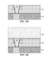
- FIG. 7 Multiple embodiments for creating poor liner coverage are shown in FIG. 7 .
- One embodiment for creating poor liner coverage is to create a higher angle at upper portion 125 of conductive via 122 .
- a further embodiment for creating poor liner coverage is to create a steep bottom sidewall 126 of conductive via 122 by creating an angle greater than 87° and a high angle, greater than 87°, at the top sidewall of conductive via 122 .
- Another embodiment for creating poor liner coverage is by undercutting sidewalls 127 and 128 of conductive via 122 , preferably such that undercut 129 is greater than 3 nm.
- the dielectric layer is reactive ion etched through a hardmask for pattern transfer. This creates a dielectric-hardmask stack where the reactive ion etched conductive via 122 has a dense hardmask material on top.
- the dielectric layer is always a less-dense material than the hardmask, which means that it tends to be more deformable and more easily etchable by, for example, reactive ion etch and wet etches. Moreover, it is more easily deformed by, for example, heating, outgassing, and moisture desorption.
- an undercut process can be performed using any low-k dielectric; however the effects of the undercut process are more pronounced using an ultra low-k dielectric. Consequently, an undercut is easy to create or engineer, simply on the basis of selection of a wet clean or reactive ion etch that is selective to the ultra low-k dielectric versus the hardmask, or to degas conditions that cause more shrinkage of the ultra low-k dielectric versus the hardmask.
- An ultra low-k dielectric material has a dielectric constant less than 2.7.
Landscapes
- Physics & Mathematics (AREA)
- General Physics & Mathematics (AREA)
- Internal Circuitry In Semiconductor Integrated Circuit Devices (AREA)
- Fuses (AREA)
- Design And Manufacture Of Integrated Circuits (AREA)
Abstract
Description
- 1. Field of the Invention
- The present invention relates to electronic fuses (e-fuses). More specifically, the present invention relates to stacked via structures for metal fuse applications.
- 2. Description of the Related Art
- In advanced technologies, e-fuses have been implemented at the polycrystalline silicon (PC) level. During programming, a high current pulse of short duration is passed through the structure. This irreversibly migrates silicide on top of the PC, causing a change in resistance and thus acting as a programmable fuse.
- As scaling progresses, it is becoming harder to implement these e-fuses at the PC level due to drop in maximum allowable currents through the first metal layer or conductor. Also, the collateral damage associated with the event is becoming more difficult to contain. As a result, there is a drive to implement these fuses at the metal interconnect levels and use the phenomenon of electromigration (EM) to program the fuses.
- The power requirements to cause EM in copper (Cu) interconnects are much larger than the typical PC level fuses. This is partly due to the fact that the liner materials used in Cu interconnects, such as tantalum (Ta) and tantalum nitride (TaN), must be blown along with the Cu in order to achieve proper fuse programming. Hence, there is a need to devise fuse structures that are susceptible to EM without compromising the reliability of the remaining interconnects.
- In a conventional metal fuse approach, as shown in
FIG. 1 , a two-level structure comprisesconductor 11 embedded indielectric layer 10, and via 21 andline 22 embedded indielectric layer 20. Acap layer 23 is typically deposited overline 22 anddielectric layer 20. Electron flow is from via 21 intoline 22. A high current is applied between the positive current connection (I+) and negative current connection (I−) to induce EM failure. Voltage across the structure is measured using the positive (V+) and negative (V−) voltage connections. The electron flow through the fuse structure is from the lower level metal,conductor 11, to the upper level metal,line 22. - With this design, some of the failures occur in via 21 while other failures occur in
line 22, resulting in a lack of control over the failure location and leading to variability in the final resistance of the fuse structure after programming. Moreover, it is not possible to electrically determine whether the failure is in via 21 orline 22. Failures inline 22 are less desirable becausecap layer 23 may be compromised during the programming process. - The programming process with this design may lead to damage in the surrounding
dielectric layer 20. It is likely that material from the blown fuse area will be present in the damaged dielectric region. If this is the case, then there is concern that the material will migrate throughout the dielectric, causing a short circuit to neighboring lines. - Therefore, a structure is needed such that failures occur preferentially in the via and not the line. Also, a detection method is needed to determine whether the programming process causes damage in the via or the line. The structure should allow for determining whether material from the blown fuse area has migrated into the dielectric region. It would also be desirable to prevent further migration of the blown fuse material.
- The present invention provides a back end of the line fuse structure. The fuse structure promotes failures in certain areas of a fuse. The present invention further provides a method for detecting where the failures occur in a fuse and a method for detecting damage in a fuse.
- According to an embodiment of the present invention, a fuse structure is provided. The fuse structure includes: a first dielectric layer having a first conductive via and a first conductive line disposed in a first cavity formed in the first dielectric layer, the first conductive via and the first conductive line having a first liner disposed along at least vertical surfaces of the first cavity; a second dielectric layer above the first dielectric layer, the second dielectric layer having a second conductive via and a second conductive line disposed in a second cavity formed in the second dielectric layer, the second conductive via and the second conductive line being in electrical contact with the first conductive via and the first conductive line, and having a second liner disposed along at least vertical surfaces of the second cavity; wherein at least a portion of the first liner has a thickness less than the second liner.
- According to a further embodiment of the present invention, another fuse structure is provided. The fuse structure includes: a first dielectric layer having a first conductive via and a first conductive line within a first dual damascene cavity formed in the first dielectric layer, the first conductive via and the first conductive line surrounded laterally by a first liner; a second dielectric layer above the first dielectric layer having a second conductive via and a second conductive line embedded within a second dual damascene cavity formed in the second dielectric layer, the second conductive via and second conductive line in electrical contact with the first conductive via and the first conductive line and surrounded laterally by a second liner; wherein the first liner surrounding laterally the first conductive via and the first conductive line has a thickness of less than about 30 nm, the second liner surrounding laterally the second conductive via and the second conductive line has a thickness of greater than about 30 nm.
- According to another embodiment of the present invention, a further fuse structure is provided. The fuse structure includes: a first dielectric layer having a first conductive via and a first conductive line disposed in a first cavity formed in the first dielectric layer, the first conductive via and the first conductive line having a first liner disposed along at least vertical surfaces of the first cavity; a second dielectric layer disposed on the first dielectric layer, the second dielectric layer having a second conductive via and a second conductive line disposed in a second cavity formed in the second dielectric layer, the second conductive via and the second conductive line being in electrical contact with the first conductive via and the first conductive line, the second conductive line laterally extending around the second conductive via such that the conductive line extends in all directions wider than at least a diameter of an upper portion of the first conductive via, and having a second liner disposed along at least vertical surfaces of the second cavity; wherein the first liner has a thickness less than the second liner.
- According to a further embodiment of the present invention, a method for electrically detecting failures in a conductive via and a conductive line is provided. The method includes the steps of: forcing current through a fuse structure between a positive current connection and a negative current connection; measuring voltage over each of a first voltage connection and a second voltage connection in the fuse structure; and detecting a failure in one of a conductive via and a conductive line; wherein failure occurs in the conductive via if an open circuit exists at both the first and second voltage connections such that there is no current flow at the voltage connections when current is forced; and wherein a failure occurs in the conductive line if an open circuit exists at only one of the first and second voltage connections such that there is no current flow at one of the voltage connections and an open circuit does not exist at the other when current is forced.
- According to another embodiment of the present invention, a method for electrically detecting damage in dielectric regions of a fuse is provided. The method includes the steps of: applying voltage between a negative current connection and an positive current connection; measuring current between a positive current connection and a negative current connection; and detecting damage in a dielectric region wherein damage exists and has extended where a short circuit is measured between the positive current connection and the negative current connection.
- According to a further embodiment of the present invention, a fuse structure for detecting material from damage by a blown fuse is provided. The fuse structure includes: a first dielectric layer disposed on the dielectric material having a first conductive via and a first conductive line disposed in a first cavity formed in the first dielectric layer, the first conductive via and the first conductive line having a first liner disposed along at least vertical surfaces of the first cavity; a second conductive via and a second conductive line disposed in a second cavity formed in the first dielectric layer and having a second liner disposed along at least vertical surfaces of the second cavity, wherein the second conductive via and the second conductive line are not in contact with the first conductive via and the first conductive line; a second dielectric layer disposed on the first dielectric layer, the second dielectric layer having a third conductive via and a third conductive line disposed in a third cavity formed in the second dielectric layer, the third conductive via and the third conductive line being in electrical contact with the first conductive via and the first conductive line, the second conductive line laterally extending around the third conductive via such that the third conductive line extends in all directions wider than at least a diameter of an upper portion of the first conductive via, and having a third liner disposed along at least vertical surfaces of the third cavity; wherein the first liner has a thickness less than the second liner.
- According to another embodiment of the present invention, a method of manufacturing a fuse structure is provided. The method includes the steps of: forming a first cavity in a first dielectric layer, the first dielectric layer disposed on a dielectric material, the dielectric material having a conductor embedded therein, the first cavity in contact with the conductor; depositing a first liner on all surfaces of the first cavity; depositing a seed layer in the first cavity; filling the first cavity with a conductive material forming a first via and a first line; depositing a second dielectric layer laterally disposed on the first cavity; forming a second cavity in the second dielectric layer; depositing a second liner on all surfaces of the first cavity; depositing a second seed layer in the cavity; and filling the second cavity with a conductive material forming a second via and a second line, the second via and the second line being in electrical contact with the first via and the first line.
- The features and elements of the present invention are set forth with respect to the appended claims and illustrated in the drawings.
-
FIG. 1 illustrates a schematic cross section of a conventional metal fuse structure. -
FIG. 2 illustrates a schematic cross section of the present invention having a stacked via metal fuse structure. -
FIG. 3 illustrates a schematic cross section of the present invention having a stacked via metal fuse structure and an extended conductive line. -
FIG. 4 illustrates a top view of the present invention having a stacked via metal fuse structure and an extended conductive line. -
FIG. 5 illustrates a schematic cross section of the present invention having a stacked via metal fuse structure, an extended conductive line and an adjacent conductive via and conductive line. -
FIGS. 6A-6I illustrate the method of manufacturing the fuse structure of the present invention. -
FIG. 7 illustrates methods for creating poor liner coverage in the fuse structure of the present invention. - The present invention provides a back end of the line (BEOL) fuse structure having a stack of vias. The stacking of vias leads to high aspect ratios, which makes liner and seed coverage inside of the vias poorer. This weakness in the liner and seed layers leads to a higher probability of electromigration (EM) failure. The present invention includes a fuse structure to address failures due to poor liner and seed coverage. Design features allow for determining the extent of the damaged region following fuse programming. Other design features make it possible to prevent further propagation of the damaged dielectric region.
- The following describes embodiments of the present invention with reference to the drawings. The embodiments are illustrations of the invention, which can be embodied in various forms. The present invention is not limited to the embodiments described below, rather representative for teaching one skilled in the art how to make and use it. Some aspects of the drawings repeat from one drawing to the next. The aspects retain their same numbering from their first appearance throughout each of the preceding drawings.
- With reference now to
FIG. 2 , a fuse structure in accordance with the present invention is shown. The fuse structure is above and in electrical contact withconductor 111 embedded indielectric material 110.Dielectric layer 120 is disposed abovedielectric material 110. Conductive via 122 andconductive line 123 are disposed incavity 121 formed indielectric layer 120. Preferably,conductive line 123 is formed above conductive via 122.Liner 124 is disposed along at least vertical surfaces ofcavity 121. Preferably,liner 124 is also disposed along a bottom surface ofcavity 121.Dielectric layer 130 is disposed abovedielectric layer 120. Conductive via 132 andconductive line 133 are disposed incavity 131 formed indielectric layer 130. Conductive via 132 andline 133 are in electrical contact with conductive via 122 andconductive line 123.Liner 134 is disposed along at least vertical surfaces ofcavity 131. Preferably,liner 134 is further disposed along ahorizontal surface 135 beneathline 133, a bottom surface ofcavity 131 and vertical surfaces ofconductive line 133. The electron flow through the fuse structure is from the lower level metal,conductor 111, through conductive via 122,conductive line 123 and conductive via 132, to the upper level metal,conductive line 133. -
Liner 124 preferably has poor coverage as compared to at least one portion ofliner 134.Liner 124 preferably has a thickness less than the thickness ofliner 134 such that upon application of high current between the positive current connection (I+) and negative voltage connection (I−) to induce electromigration (EM) failure, failure occurs preferentially in conductive via 122 rather than in conductive via 132 orconductive line 133. Specifically,liner 124 preferably has a thickness of less than about 30 nm andliner 134 preferably has a thickness of greater than about 30 nm. In this structure, EM failures are more likely to occur in conductive via 122 rather than in conductive via 132 orconductive line 133, because relatively lower power is required to cause a failure in conductive via 122 due to the poor coverage ofliner 124. - Any suitable dielectric material may be used for
dielectric material 110 anddielectric layers dielectrics - A dielectric barrier layer or capping layer is disposed above each of
dielectric material 110 anddielectric layers - Any suitable liner material may be used for
liners liners - Any suitable conductive material may be used for
conductor 111, conductive via 122,conductive line 123, conductive via 132 andconductive line 133. The material used for each ofconductor 111, conductive via 122,conductive line 123, conductive via 132 andconductive line 133 may be the same or different. Typical conductive materials include copper (Cu), aluminum (Al), silver (Ag), gold (Au) and alloys. - Due to the nature of the liner deposition process, liner coverage in the via depends on which via sidewall is being covered. In the case of Ta and TaN, a physical vapor deposition (PVD) process is used such that the line feature above the via will affect the liner coverage in the via. The same holds for the Cu seed layer that is deposited by PVD following liner deposition. In
FIG. 1 , poor liner coverage occurs on viasidewall 24 that is opposite to anend 25 ofline 22 while good liner coverage occurs on the other viasidewall 26. This is a result of a dielectric shadowing effect in which the presence of a line end prevents liner material from adequately coating the opposite via sidewall. This represents a less than ideal situation since vias with good liner coverage will require higher power to be blown. - In order to combat the shadowing effect, a further embodiment of the present invention permits good liner and seed coverage throughout conductive via 132, because failures may still occur in conductive via 132 and
conductive line 133. In a preferred embodiment of the present invention, liner coverage can be influenced by the extent to which the line opening extends laterally beyond the via opening. As shown inFIG. 2 ,conductive line 133 extends laterally beyond aside 136 of conductive via 132.Conductive line 133 can also extend laterally around conductive via 132 by a certain distance in all directions, as seen inFIG. 3 . The extension will ensure good liner and seed coverage onsidewalls conductive line 133 much wider than the diameter of an upper portion of conductive via 122 in all directions, as seen inFIG. 4 , ensures that all sidewalls of conductive via 132 receive good liner and seed coverage. As the width ofconductive line 133 increases in all directions, liner and seed coverage of conductive via 132 continues to improve in all directions. The improvement in liner and seed coverage of conductive via 132 reduces the potential for failures occurring in conductive via 132 andconductive line 133 and promotes failures in conductive via 122. - Extending
conductive line 133 also provides the ability to electrically distinguish between failures in conductive via 122, conductive via 132 andconductive line 133. Following fuse programming where a high current is forced through the fuse structure to blow the fuse, current is forced between a positive current connection (I+) atconductive line 133 and a negative current connection (I−) atconductor 111. The voltage across the structure would be measured over a positive voltage connection (V+) alongconductive line 133 and a negative voltage connection (V−) atconductor 111. If an open circuit is measured at both of the positive (V+) voltage connections and the negative (V−) voltage connection, then the failure occurred in a conductive via, for example conductive via 122 inFIG. 3 . Thus, there is no current flow at the voltage connections when current is forced. However, if an open circuit exists only at one of the positive voltage connections, then the failure occurs in a conductive line, for exampleconductive line 133 inFIG. 3 . This testing can be used to screen parts such that only via failures are allowed in a product. - Forcing high current through the fuse structure during fuse programming will likely lead to damage in the surrounding dielectric layer. If conductive via 122 fails, then the resulting damage could be electrically detected by placing vias and lines next to the fuse structure, shown in
FIG. 5 as conductive via 142 andconductive line 143. Referring toFIG. 5 , detection is made by applying a voltage between a negative voltage connection (V−) and positive voltage connection (V+) and then measuring the current between the positive current connection (I+) and a negative current connection (I−). Negative voltage and current connections are located atconductor 111 and alongconductive line 133. Positive voltage and current connections are located at conductive via 142 andconductive line 143. If a short circuit is measured, then the damaged region has extended too far and may lead to reliability concerns. The programming conditions would then be adjusted to produce less damage. - The fuse structure shown in
FIG. 2 may be formed using the process shown inFIGS. 6A-6I . First,dielectric layer 120 is deposited ondielectric material 110 havingconductor 111 embedded therein. An opening orcavity 121 for conductive via 122 andconductive line 123 is next formed indielectric layer 120. Preferably,cavity 121 may be a dual damascene cavity to provide openings for conductive via 122 andconductive line 123 simultaneously.Liner 124 is then deposited on at least vertical surfaces ofcavity 121 by a physical vapor deposition (PVD) or chemical vapor deposition (CVD) process for example. Preferably,liner 124 is deposited on the bottom surface ofcavity 121 as well. A Cu seed layer is deposited by PVD incavity 121.Cavity 121 withliner 124 is then filled with a conductive material such as Cu using, for example, an electroplating process, to form conductive via 122 andconductive line 123. Via 142 andline 143, as shown inFIG. 5 , are also optionally formed by an electroplating process, for example, indielectric layer 120. - Next,
dielectric layer 130 is deposited onlayer 120, an opening orcavity 131 is formed indielectric layer 130,liner 134 is deposited on surfaces ofcavity 131, a Cu seed layer is deposited andcavity 131 is filled with a conductive material to form conductive via 132 andconductive line 133. Optionally,conductive line 133 is formed in such a way as to extend in all directions around conductive via 132. -
Dielectric layers -
Cavity 121 may be formed using any suitable lithographic patterning and etching process.Conductive vias conductive lines - A physical vapor deposition (PVD) process is used to deposit liner materials such as Ta and TaN. Other deposition processes, such as chemical vapor deposition (CVD) and atomic layer deposition (ALD), may be used to deposit liner materials as well.
- To promote a failure in the lower via as opposed to the upper via or line, it is preferred to create poor liner coverage in conductive via 122 and good liner coverage in conductive via 132. Multiple embodiments for creating poor liner coverage are shown in
FIG. 7 . One embodiment for creating poor liner coverage is to create a higher angle atupper portion 125 of conductive via 122. A further embodiment for creating poor liner coverage is to create a steepbottom sidewall 126 of conductive via 122 by creating an angle greater than 87° and a high angle, greater than 87°, at the top sidewall of conductive via 122. Another embodiment for creating poor liner coverage is by undercuttingsidewalls - In order to undercut
sidewalls - The terminology used herein is for the purpose of describing particular embodiments only and is not intended to be limiting of the invention. As used herein, the singular forms “a”, “an” and “the” are intended to include the plural forms as well, unless the context clearly indicates otherwise. It will be further understood that the terms “comprises” and/or “comprising,” when used in this specification, specify the presence of stated features, integers, steps, operations, elements, and/or components, but do not preclude the presence or addition of one or more other features, integers, steps, operations, elements, components, and/or groups thereof.
- The corresponding structures, materials, acts, and equivalents of all means or step plus function elements in the claims below are intended to include any structure, material, or act for performing the function in combination with other claimed elements as specifically claimed. The description of the present invention has been presented for purposes of illustration and description, but is not intended to be exhaustive or limited to the invention in the form disclosed. Many modifications and variations will be apparent to those of ordinary skill in the art without departing from the scope and spirit of the invention. The embodiment was chosen and described in order to best explain the principles of the invention and the practical application, and to enable others of ordinary skill in the art to understand the invention for various embodiments with various modifications as are suited to the particular use contemplated.
Claims (24)
Priority Applications (10)
| Application Number | Priority Date | Filing Date | Title |
|---|---|---|---|
| US13/074,407 US8633707B2 (en) | 2011-03-29 | 2011-03-29 | Stacked via structure for metal fuse applications |
| CN201610161586.9A CN105810668B (en) | 2011-03-29 | 2012-03-13 | For the stacked channels structure of metal fuse application |
| CN201280016328.1A CN103460380B (en) | 2011-03-29 | 2012-03-13 | Stacked channel structure for metal fuse applications |
| DE112012001490.1T DE112012001490B4 (en) | 2011-03-29 | 2012-03-13 | Stacked via structure for metal fuse applications |
| CN201610161575.0A CN105655324B (en) | 2011-03-29 | 2012-03-13 | Stacked channel structure for metal fuse applications |
| PCT/US2012/028847 WO2012134801A2 (en) | 2011-03-29 | 2012-03-13 | Stacked via structure for metal fuse applications |
| DE112012007315.0T DE112012007315B3 (en) | 2011-03-29 | 2012-03-13 | METHOD FOR ELECTRICAL DETECTION OF DAMAGE TO A STACKED THROUGH CONTACT STRUCTURE FOR METAL FUSE APPLICATIONS |
| US14/040,945 US8742766B2 (en) | 2011-03-29 | 2013-09-30 | Stacked via structure for metal fuse applications |
| US14/188,728 US9360525B2 (en) | 2011-03-29 | 2014-02-25 | Stacked via structure for metal fuse applications |
| US15/072,400 US10229875B2 (en) | 2011-03-29 | 2016-03-17 | Stacked via structure for metal fuse applications |
Applications Claiming Priority (1)
| Application Number | Priority Date | Filing Date | Title |
|---|---|---|---|
| US13/074,407 US8633707B2 (en) | 2011-03-29 | 2011-03-29 | Stacked via structure for metal fuse applications |
Related Child Applications (1)
| Application Number | Title | Priority Date | Filing Date |
|---|---|---|---|
| US14/040,945 Division US8742766B2 (en) | 2011-03-29 | 2013-09-30 | Stacked via structure for metal fuse applications |
Publications (2)
| Publication Number | Publication Date |
|---|---|
| US20120249159A1 true US20120249159A1 (en) | 2012-10-04 |
| US8633707B2 US8633707B2 (en) | 2014-01-21 |
Family
ID=46926368
Family Applications (4)
| Application Number | Title | Priority Date | Filing Date |
|---|---|---|---|
| US13/074,407 Active 2032-04-10 US8633707B2 (en) | 2011-03-29 | 2011-03-29 | Stacked via structure for metal fuse applications |
| US14/040,945 Expired - Fee Related US8742766B2 (en) | 2011-03-29 | 2013-09-30 | Stacked via structure for metal fuse applications |
| US14/188,728 Active 2031-09-09 US9360525B2 (en) | 2011-03-29 | 2014-02-25 | Stacked via structure for metal fuse applications |
| US15/072,400 Active 2031-06-28 US10229875B2 (en) | 2011-03-29 | 2016-03-17 | Stacked via structure for metal fuse applications |
Family Applications After (3)
| Application Number | Title | Priority Date | Filing Date |
|---|---|---|---|
| US14/040,945 Expired - Fee Related US8742766B2 (en) | 2011-03-29 | 2013-09-30 | Stacked via structure for metal fuse applications |
| US14/188,728 Active 2031-09-09 US9360525B2 (en) | 2011-03-29 | 2014-02-25 | Stacked via structure for metal fuse applications |
| US15/072,400 Active 2031-06-28 US10229875B2 (en) | 2011-03-29 | 2016-03-17 | Stacked via structure for metal fuse applications |
Country Status (4)
| Country | Link |
|---|---|
| US (4) | US8633707B2 (en) |
| CN (3) | CN105655324B (en) |
| DE (2) | DE112012007315B3 (en) |
| WO (1) | WO2012134801A2 (en) |
Cited By (7)
| Publication number | Priority date | Publication date | Assignee | Title |
|---|---|---|---|---|
| US20130147008A1 (en) * | 2011-12-09 | 2013-06-13 | Globalfoundries Inc. | Metal E-Fuse With Intermetallic Compound Programming Mechanism and Methods of Making Same |
| US20140217612A1 (en) * | 2013-02-06 | 2014-08-07 | International Business Machines Corporation | Electronic fuse having a damaged region |
| US20140266286A1 (en) * | 2013-03-13 | 2014-09-18 | Qualcomm Incorporated | Through-substrate via with a fuse structure |
| US9087842B2 (en) | 2013-10-22 | 2015-07-21 | Samsung Electronics Co., Ltd. | Semiconductor device including fuse structure |
| US9099469B2 (en) | 2013-10-11 | 2015-08-04 | Samsung Electronics Co., Ltd. | E-fuse structure of semiconductor device |
| US9214245B2 (en) | 2014-01-23 | 2015-12-15 | Samsung Electronics Co., Ltd. | E-fuse structure of semiconductor device |
| US12406878B2 (en) * | 2013-12-12 | 2025-09-02 | Taiwan Semiconductor Manufacturing Company, Ltd. | Integrated circuit with conductive line having line-ends |
Families Citing this family (14)
| Publication number | Priority date | Publication date | Assignee | Title |
|---|---|---|---|---|
| US8633707B2 (en) * | 2011-03-29 | 2014-01-21 | International Business Machines Corporation | Stacked via structure for metal fuse applications |
| TWI496256B (en) * | 2012-12-28 | 2015-08-11 | 財團法人工業技術研究院 | Biaxial perforation bidirectional repair circuit for semiconductor device |
| JP2015159240A (en) * | 2014-02-25 | 2015-09-03 | 矢崎総業株式会社 | flexible flat circuit body |
| TWI620290B (en) | 2014-05-27 | 2018-04-01 | 聯華電子股份有限公司 | Conductive pad structure and manufacturing method thereof |
| US9536829B2 (en) | 2014-09-11 | 2017-01-03 | Internatonal Business Machines Corporation | Programmable electrical fuse in keep out zone |
| KR101676810B1 (en) | 2014-10-30 | 2016-11-16 | 삼성전자주식회사 | Semiconductor device and display driver IC including the same and display device including the same |
| US9704802B2 (en) * | 2015-08-28 | 2017-07-11 | Micron Technology, Inc. | Integrated circuit structures comprising conductive vias and methods of forming conductive vias |
| US9984967B2 (en) | 2015-12-21 | 2018-05-29 | Taiwan Semiconductor Manufacturing Company, Ltd. | Semiconductor structure and manufacturing method thereof |
| US9666528B1 (en) | 2016-02-23 | 2017-05-30 | International Business Machines Corporation | BEOL vertical fuse formed over air gap |
| US9978678B1 (en) | 2017-02-02 | 2018-05-22 | International Business Machines Corporation | Vertically integrated nanosheet fuse |
| US10157824B2 (en) | 2017-05-05 | 2018-12-18 | Qualcomm Incorporated | Integrated circuit (IC) package and package substrate comprising stacked vias |
| US10935590B2 (en) * | 2017-10-17 | 2021-03-02 | Infineon Technologies Ag | Electrically-verifiable fuses and method of fuse verification |
| CN108598064B (en) * | 2018-05-09 | 2020-05-15 | 北京智芯微电子科技有限公司 | Metal wires connecting regular chips in wafers to test-specific chips |
| US20200111741A1 (en) * | 2018-10-09 | 2020-04-09 | International Business Machines Corporation | Vertical electrical fuse |
Citations (2)
| Publication number | Priority date | Publication date | Assignee | Title |
|---|---|---|---|---|
| US7704805B1 (en) * | 2003-12-12 | 2010-04-27 | Marvell International Ltd. | Fuse structures, methods of making and using the same, and integrated circuits including the same |
| US20120126363A1 (en) * | 2010-11-23 | 2012-05-24 | International Business Machines Corporation | Structure of metal e-fuse |
Family Cites Families (45)
| Publication number | Priority date | Publication date | Assignee | Title |
|---|---|---|---|---|
| JPS5834945B2 (en) * | 1980-06-02 | 1983-07-29 | 株式会社東芝 | Fuse type PROM semiconductor device |
| US6100118A (en) | 1998-06-11 | 2000-08-08 | Taiwan Semiconductor Manufacturing Company, Ltd. | Fabrication of metal fuse design for redundancy technology having a guard ring |
| US6100116A (en) | 1998-06-18 | 2000-08-08 | Taiwan Semiconductor Manufacturing Company | Method to form a protected metal fuse |
| US6242789B1 (en) | 1999-02-23 | 2001-06-05 | Infineon Technologies North America Corp. | Vertical fuse and method of fabrication |
| US6157583A (en) | 1999-03-02 | 2000-12-05 | Motorola, Inc. | Integrated circuit memory having a fuse detect circuit and method therefor |
| DE19926107C1 (en) | 1999-06-08 | 2000-11-16 | Siemens Ag | Semiconductor structure, especially a memory including redundant memory cells or word lines, has a vertical fuse embedded in a cavity of a semiconductor body |
| US6295721B1 (en) * | 1999-12-28 | 2001-10-02 | Taiwan Semiconductor Manufacturing Company | Metal fuse in copper dual damascene |
| US6370074B1 (en) | 2000-05-05 | 2002-04-09 | Agere Systems Guardian Corp | Redundant encoding for buried metal fuses |
| US7186648B1 (en) | 2001-03-13 | 2007-03-06 | Novellus Systems, Inc. | Barrier first method for single damascene trench applications |
| TW504792B (en) | 2001-04-06 | 2002-10-01 | United Microelectronics Corp | Method to form metal fuse |
| US6611039B2 (en) | 2001-09-28 | 2003-08-26 | Hewlett-Packard Development Company, L.P. | Vertically oriented nano-fuse and nano-resistor circuit elements |
| US6555458B1 (en) | 2002-01-14 | 2003-04-29 | Taiwan Semiconductor Manufacturing Co., Ltd. | Fabricating an electrical metal fuse |
| US6900533B2 (en) | 2002-01-30 | 2005-05-31 | Agilent Technologies, Inc. | Apparatus for routing electrical signals |
| US6444503B1 (en) | 2002-02-07 | 2002-09-03 | Taiwan Semiconductor Manufacturing Company | Fabricating electrical metal fuses without additional masking |
| US6638796B2 (en) | 2002-02-13 | 2003-10-28 | Taiwan Semiconductor Manufacturing Company | Method of forming a novel top-metal fuse structure |
| JP2003332426A (en) * | 2002-05-17 | 2003-11-21 | Renesas Technology Corp | Semiconductor device manufacturing method and semiconductor device |
| US6753210B2 (en) | 2002-09-17 | 2004-06-22 | Taiwan Semiconductor Manufacturing Company | Metal fuse for semiconductor devices |
| US6835642B2 (en) | 2002-12-18 | 2004-12-28 | Taiwan Semiconductor Manufacturing Co., Ltd | Method of forming a metal fuse on semiconductor devices |
| KR100507702B1 (en) | 2003-04-03 | 2005-08-09 | 주식회사 하이닉스반도체 | Method of forming a metal line in a semiconductor device |
| JP2004335735A (en) | 2003-05-07 | 2004-11-25 | Toshiba Corp | Semiconductor device |
| US7098537B2 (en) * | 2003-11-21 | 2006-08-29 | International Business Machines Corporation | Interconnect structure diffusion barrier with high nitrogen content |
| DE102004014925B4 (en) * | 2004-03-26 | 2016-12-29 | Infineon Technologies Ag | Electronic circuit arrangement |
| JP2006005180A (en) * | 2004-06-18 | 2006-01-05 | Matsushita Electric Ind Co Ltd | Semiconductor device and inspection method of semiconductor device |
| US20050285222A1 (en) * | 2004-06-29 | 2005-12-29 | Kong-Beng Thei | New fuse structure |
| US7342198B2 (en) * | 2005-08-05 | 2008-03-11 | 3Sae Technologies, Inc. | Method and apparatus for generating an electrical arc |
| US20070063310A1 (en) | 2005-09-19 | 2007-03-22 | Taiwan Semiconductor Manufacturing Company, Ltd. | A metal fuse for semiconductor devices and methods of manufacturing thereof |
| CN100460870C (en) * | 2005-11-02 | 2009-02-11 | 中芯国际集成电路制造(上海)有限公司 | Method and device for testing oxide of grid electrode by using fuse wire |
| JP4921949B2 (en) | 2006-01-20 | 2012-04-25 | 株式会社東芝 | Semiconductor device |
| KR100735529B1 (en) | 2006-02-09 | 2007-07-04 | 삼성전자주식회사 | Semiconductor memory device and manufacturing method thereof |
| US7528066B2 (en) | 2006-03-01 | 2009-05-05 | International Business Machines Corporation | Structure and method for metal integration |
| US7339486B2 (en) | 2006-03-06 | 2008-03-04 | Hansor Polymer Technology Corp. | Insertion type fuse with breakage indication |
| JP4861051B2 (en) * | 2006-05-09 | 2012-01-25 | ルネサスエレクトロニクス株式会社 | Semiconductor device and electrical fuse cutting method |
| JP4871031B2 (en) * | 2006-06-06 | 2012-02-08 | ルネサスエレクトロニクス株式会社 | Semiconductor device and fuse determination method |
| KR100808593B1 (en) | 2006-07-28 | 2008-02-29 | 주식회사 하이닉스반도체 | Fuse box of semiconductor device and forming method thereof |
| US7785934B2 (en) * | 2007-02-28 | 2010-08-31 | International Business Machines Corporation | Electronic fuses in semiconductor integrated circuits |
| US8749020B2 (en) | 2007-03-09 | 2014-06-10 | Taiwan Semiconductor Manufacturing Company, Ltd. | Metal e-fuse structure design |
| US20080289695A1 (en) | 2007-05-21 | 2008-11-27 | Holzer Robert C | Heat activated automatic gas shut-off valve |
| US8232190B2 (en) * | 2007-10-01 | 2012-07-31 | International Business Machines Corporation | Three dimensional vertical E-fuse structures and methods of manufacturing the same |
| US7642176B2 (en) * | 2008-04-21 | 2010-01-05 | Taiwan Semiconductor Manufacturing Company, Ltd. | Electrical fuse structure and method |
| US7956466B2 (en) * | 2008-05-09 | 2011-06-07 | International Business Machines Corporation | Structure for interconnect structure containing various capping materials for electrical fuse and other related applications |
| US7893520B2 (en) * | 2008-05-12 | 2011-02-22 | International Business Machines Corporation | Efficient interconnect structure for electrical fuse applications |
| US9263384B2 (en) * | 2008-05-13 | 2016-02-16 | Infineon Technologies Ag | Programmable devices and methods of manufacture thereof |
| JP5510862B2 (en) * | 2009-03-10 | 2014-06-04 | ルネサスエレクトロニクス株式会社 | Semiconductor device |
| KR101110793B1 (en) * | 2009-07-01 | 2012-03-13 | 주식회사 하이닉스반도체 | Semiconductor device |
| US8633707B2 (en) | 2011-03-29 | 2014-01-21 | International Business Machines Corporation | Stacked via structure for metal fuse applications |
-
2011
- 2011-03-29 US US13/074,407 patent/US8633707B2/en active Active
-
2012
- 2012-03-13 WO PCT/US2012/028847 patent/WO2012134801A2/en not_active Ceased
- 2012-03-13 CN CN201610161575.0A patent/CN105655324B/en active Active
- 2012-03-13 CN CN201610161586.9A patent/CN105810668B/en active Active
- 2012-03-13 CN CN201280016328.1A patent/CN103460380B/en active Active
- 2012-03-13 DE DE112012007315.0T patent/DE112012007315B3/en active Active
- 2012-03-13 DE DE112012001490.1T patent/DE112012001490B4/en active Active
-
2013
- 2013-09-30 US US14/040,945 patent/US8742766B2/en not_active Expired - Fee Related
-
2014
- 2014-02-25 US US14/188,728 patent/US9360525B2/en active Active
-
2016
- 2016-03-17 US US15/072,400 patent/US10229875B2/en active Active
Patent Citations (2)
| Publication number | Priority date | Publication date | Assignee | Title |
|---|---|---|---|---|
| US7704805B1 (en) * | 2003-12-12 | 2010-04-27 | Marvell International Ltd. | Fuse structures, methods of making and using the same, and integrated circuits including the same |
| US20120126363A1 (en) * | 2010-11-23 | 2012-05-24 | International Business Machines Corporation | Structure of metal e-fuse |
Cited By (13)
| Publication number | Priority date | Publication date | Assignee | Title |
|---|---|---|---|---|
| US20130147008A1 (en) * | 2011-12-09 | 2013-06-13 | Globalfoundries Inc. | Metal E-Fuse With Intermetallic Compound Programming Mechanism and Methods of Making Same |
| US8610243B2 (en) * | 2011-12-09 | 2013-12-17 | Globalfoundries Inc. | Metal e-fuse with intermetallic compound programming mechanism and methods of making same |
| US20140217612A1 (en) * | 2013-02-06 | 2014-08-07 | International Business Machines Corporation | Electronic fuse having a damaged region |
| US9059170B2 (en) * | 2013-02-06 | 2015-06-16 | International Business Machines Corporation | Electronic fuse having a damaged region |
| CN105051885A (en) * | 2013-02-06 | 2015-11-11 | 国际商业机器公司 | Electronic fuse having a damaged region |
| US20140266286A1 (en) * | 2013-03-13 | 2014-09-18 | Qualcomm Incorporated | Through-substrate via with a fuse structure |
| US9099469B2 (en) | 2013-10-11 | 2015-08-04 | Samsung Electronics Co., Ltd. | E-fuse structure of semiconductor device |
| US9368445B2 (en) | 2013-10-11 | 2016-06-14 | Samsung Electronics Co., Ltd. | E-fuse structure of semiconductor device |
| US9087842B2 (en) | 2013-10-22 | 2015-07-21 | Samsung Electronics Co., Ltd. | Semiconductor device including fuse structure |
| US12406878B2 (en) * | 2013-12-12 | 2025-09-02 | Taiwan Semiconductor Manufacturing Company, Ltd. | Integrated circuit with conductive line having line-ends |
| US9214245B2 (en) | 2014-01-23 | 2015-12-15 | Samsung Electronics Co., Ltd. | E-fuse structure of semiconductor device |
| US9666526B2 (en) | 2014-01-23 | 2017-05-30 | Samsung Electronics Co., Ltd. | E-fuse structure of semiconductor device |
| US9935049B2 (en) | 2014-01-23 | 2018-04-03 | Samsung Electronics Co., Ltd. | E-fuse structure of semiconductor device |
Also Published As
| Publication number | Publication date |
|---|---|
| WO2012134801A2 (en) | 2012-10-04 |
| US20140028325A1 (en) | 2014-01-30 |
| CN105655324A (en) | 2016-06-08 |
| CN103460380B (en) | 2016-05-18 |
| US20140167772A1 (en) | 2014-06-19 |
| US8633707B2 (en) | 2014-01-21 |
| CN103460380A (en) | 2013-12-18 |
| US8742766B2 (en) | 2014-06-03 |
| US9360525B2 (en) | 2016-06-07 |
| US10229875B2 (en) | 2019-03-12 |
| DE112012001490T5 (en) | 2013-12-24 |
| US20160197039A1 (en) | 2016-07-07 |
| DE112012007315B3 (en) | 2021-04-22 |
| CN105810668A (en) | 2016-07-27 |
| CN105810668B (en) | 2018-07-03 |
| CN105655324B (en) | 2019-04-09 |
| WO2012134801A3 (en) | 2013-01-03 |
| DE112012001490B4 (en) | 2021-02-11 |
Similar Documents
| Publication | Publication Date | Title |
|---|---|---|
| US10229875B2 (en) | Stacked via structure for metal fuse applications | |
| US9425144B2 (en) | Metal fuse structure for improved programming capability | |
| US9093164B2 (en) | Redundant via structure for metal fuse applications | |
| US9171801B2 (en) | E-fuse with hybrid metallization | |
| US9059170B2 (en) | Electronic fuse having a damaged region | |
| US9431346B2 (en) | Graphene-metal E-fuse | |
| WO2008014193A2 (en) | Electrically inactive via for electromigration reliability improvement | |
| US9064871B2 (en) | Vertical electronic fuse | |
| US9129964B2 (en) | Programmable electrical fuse | |
| US20140077334A1 (en) | Electronic Fuse Vias in Interconnect Structures | |
| US9324655B2 (en) | Modified via bottom for beol via efuse | |
| US9093452B2 (en) | Electronic fuse with resistive heater | |
| US20190326215A1 (en) | Metal embedded low-resistance beol antifuse | |
| US8723321B2 (en) | Copper interconnects with improved electromigration lifetime | |
| JP2009099833A (en) | Semiconductor device and manufacturing method thereof |
Legal Events
| Date | Code | Title | Description |
|---|---|---|---|
| AS | Assignment |
Owner name: INTERNATIONAL BUSINESS MACHINES CORPORATION, NEW Y Free format text: ASSIGNMENT OF ASSIGNORS INTEREST;ASSIGNORS:FILIPPI, RONALD G.;BONILLA, GRISELDA;CHANDA, KAUSHIK;AND OTHERS;SIGNING DATES FROM 20110321 TO 20110328;REEL/FRAME:026041/0644 |
|
| STCF | Information on status: patent grant |
Free format text: PATENTED CASE |
|
| FPAY | Fee payment |
Year of fee payment: 4 |
|
| AS | Assignment |
Owner name: SONY CORPORATION, JAPAN Free format text: ASSIGNMENT OF ASSIGNORS INTEREST;ASSIGNOR:INTERNATIONAL BUSINESS MACHINES CORPORATION;REEL/FRAME:053681/0762 Effective date: 20200712 |
|
| MAFP | Maintenance fee payment |
Free format text: PAYMENT OF MAINTENANCE FEE, 8TH YEAR, LARGE ENTITY (ORIGINAL EVENT CODE: M1552); ENTITY STATUS OF PATENT OWNER: LARGE ENTITY Year of fee payment: 8 |
|
| MAFP | Maintenance fee payment |
Free format text: PAYMENT OF MAINTENANCE FEE, 12TH YEAR, LARGE ENTITY (ORIGINAL EVENT CODE: M1553); ENTITY STATUS OF PATENT OWNER: LARGE ENTITY Year of fee payment: 12 |