US20110240325A1 - Printed Wiring Board and Electronic Apparatus - Google Patents
Printed Wiring Board and Electronic Apparatus Download PDFInfo
- Publication number
- US20110240325A1 US20110240325A1 US13/034,495 US201113034495A US2011240325A1 US 20110240325 A1 US20110240325 A1 US 20110240325A1 US 201113034495 A US201113034495 A US 201113034495A US 2011240325 A1 US2011240325 A1 US 2011240325A1
- Authority
- US
- United States
- Prior art keywords
- printed wiring
- wiring board
- silk
- punching
- board body
- Prior art date
- Legal status (The legal status is an assumption and is not a legal conclusion. Google has not performed a legal analysis and makes no representation as to the accuracy of the status listed.)
- Abandoned
Links
Images


Classifications
-
- H—ELECTRICITY
- H05—ELECTRIC TECHNIQUES NOT OTHERWISE PROVIDED FOR
- H05K—PRINTED CIRCUITS; CASINGS OR CONSTRUCTIONAL DETAILS OF ELECTRIC APPARATUS; MANUFACTURE OF ASSEMBLAGES OF ELECTRICAL COMPONENTS
- H05K3/00—Apparatus or processes for manufacturing printed circuits
- H05K3/0011—Working of insulating substrates or insulating layers
- H05K3/0044—Mechanical working of the substrate, e.g. drilling or punching
- H05K3/0052—Depaneling, i.e. dividing a panel into circuit boards; Working of the edges of circuit boards
-
- H—ELECTRICITY
- H05—ELECTRIC TECHNIQUES NOT OTHERWISE PROVIDED FOR
- H05K—PRINTED CIRCUITS; CASINGS OR CONSTRUCTIONAL DETAILS OF ELECTRIC APPARATUS; MANUFACTURE OF ASSEMBLAGES OF ELECTRICAL COMPONENTS
- H05K2201/00—Indexing scheme relating to printed circuits covered by H05K1/00
- H05K2201/09—Shape and layout
- H05K2201/09818—Shape or layout details not covered by a single group of H05K2201/09009 - H05K2201/09809
- H05K2201/09909—Special local insulating pattern, e.g. as dam around component
-
- H—ELECTRICITY
- H05—ELECTRIC TECHNIQUES NOT OTHERWISE PROVIDED FOR
- H05K—PRINTED CIRCUITS; CASINGS OR CONSTRUCTIONAL DETAILS OF ELECTRIC APPARATUS; MANUFACTURE OF ASSEMBLAGES OF ELECTRICAL COMPONENTS
- H05K2203/00—Indexing scheme relating to apparatus or processes for manufacturing printed circuits covered by H05K3/00
- H05K2203/01—Tools for processing; Objects used during processing
- H05K2203/0182—Using a temporary spacer element or stand-off during processing
-
- H—ELECTRICITY
- H05—ELECTRIC TECHNIQUES NOT OTHERWISE PROVIDED FOR
- H05K—PRINTED CIRCUITS; CASINGS OR CONSTRUCTIONAL DETAILS OF ELECTRIC APPARATUS; MANUFACTURE OF ASSEMBLAGES OF ELECTRICAL COMPONENTS
- H05K3/00—Apparatus or processes for manufacturing printed circuits
- H05K3/22—Secondary treatment of printed circuits
- H05K3/28—Applying non-metallic protective coatings
Definitions
- Embodiments described herein relate generally to a printed wiring board and an electronic apparatus.
- PCBs used in electronic apparatuses, such as personal computers, and printed wiring boards (PWBs) configured by mounted-components have various shapes depending on the finished-products thereof.
- each PWB is formed as a part of a shape in which a main piece to be formed into a finished-product of a PWB and an end member (waste member) are combined.
- the main piece and the end member are connected by perforated members, and the end member is separated from the main piece as a product part by punching.
- JP-S62-098795-A discloses a technique of processing the material without making a metal pressing impact on a coating film during outline machining.
- One surface of the board exemplified in JP-S62-098795-A to be put on a mold is flat.
- wiring patterns may be provided on both surfaces of the product part.
- air-gaps may be generated between the mold and the board body by irregularities due to the patterns. For example, when the air-gaps are positioned in the boundary between the main piece and the end member, the board body cannot sufficiently be supported on the mold and thus bends. This may result in damage of the product part.
- FIG. 1 schematically illustrates an electronic apparatus according to an embodiment.
- FIG. 2 illustrates electronic components mounted on a printed wiring board according to the embodiment before punched.
- FIG. 3 illustrates a connecting part of the printed wiring board according to the embodiment.
- FIG. 4 sectionally illustrates the printed wiring board according to the embodiment.
- FIG. 5 illustrates a process operation according to the embodiment performed before a punching-cut operation.
- FIG. 6 illustrates the punching-cut operation
- FIG. 7 illustrates a modification of the embodiment.
- FIG. 8 illustrates a printed wiring board according to a second embodiment.
- FIG. 9 illustrates a printed wiring board according to a third embodiment.
- FIG. 10 illustrates a printed wiring board according to a fourth embodiment.
- a printed wiring board including: a board body having a first surface and a second surface opposite thereto, a product part defined in the board body, at which a wiring pattern is formed; an end part defined in the board body, at a position separated from the product part; a connecting part defined in the board body, through which the product part and the end part are connected; and a coating-material applied on the first surface of the board body along the connecting part.
- FIG. 1 schematically illustrates an electronic apparatus according to an embodiment in which a notebook type personal computer is exemplified.
- a personal computer (electronic apparatus) 100 includes a display portion 100 A and a body portion 100 B.
- the display portion 100 A and the body portion 100 B are openably connected to each other by a hinge portion 15 .
- the body portion 100 B has a lower casing 20 .
- the lower casing 20 houses a function portion 2 having a printed wiring board 201 (printed wiring board), on which electronic components such as a central processing unit (CPU) and a memory are mounted, and that processes information.
- CPU central processing unit
- the lower casing 20 has a top surface 20 a , a bottom surface 20 b , a left side surface 20 e , a right side surface 20 f , a front surface 20 g , and a rear surface 20 h .
- the lower casing 20 houses a character input portion 3 , such as a keyboard, for inputting characters and commands, a track pad 4 A serving as a pointing device, a decision switch 4 B for inputting selection and decision commands, and a fingerprint reading portion 5 used to authenticate users. Openings 20 A to 20 D are formed in the top surface 20 a . A depression portion 21 is formed around the opening 20 D.
- the character input portion 3 is exposed from the opening 20 A.
- the track pad 4 A is exposed from the opening 20 B.
- the decision switch 4 B is exposed from the opening 20 C.
- the fingerprint reading portion 5 is exposed from the opening 20 D.
- the display portion 100 A has an upper casing 10 .
- the upper casing 10 houses an image display portion 1 including a liquid crystal panel or the like for displaying characters, images and the like.
- the upper casing 10 has a front surface 20 i .
- An opening 20 E is formed in the front surface 20 i .
- the image display portion 1 is exposed from the opening 20 E.
- a printed wiring board 201 housed in the personal computer 100 can have various shapes depending on a mounted component in the casing and the product size thereof.
- the printed wiring board 201 Before loaded into a mounting line, the printed wiring board 201 is manufactured as a part of a plate-like member in which a product part (to be formed into the printed wiring board 201 ) and an end member are combined, in view of enhancing workability and manufacturability. After supplied to the mounting line, the product part and the end member are separated from each other by punching.
- FIG. 2 illustrates the printed wiring board 201 before punched.
- FIG. 3 illustrates a connecting part of the printed wiring board 201 .
- FIG. 4 sectionally illustrates the printed wiring board 201 .
- the printed wiring board 201 includes a product part 301 (product part) on which an electronic component (not shown) is mounted, an end member 302 (end part) provided around the product part 301 to have an air-gap between the product part 301 and the end member 302 , and a connecting part 303 (connecting part) which connects the product part 301 to the end member 302 .
- a silk 301 a (coating-material) is applied over the product part 301 and the end member 302 on the printed wiring board 201 according to the present embodiment.
- the silk 301 a is applied around the connecting part 303 .
- the silk 301 a is applied to at least an area extending over the product part 301 and the connecting part 303 .
- the “silk” is a coating-material such as oil-based ink using, e.g., a volatile organic solvent, and aqueous ink that uses water as a solvent so as to be water-resist after dried.
- a silk 301 A showing characters indicating an electronic component mounting area and/or product information is provided on the printed wiring board 201 .
- the silk 301 a to be provided around, e.g., the connecting part 303 is applied onto the same surface as that to which the silk 301 A is applied.
- Such configuration can be accomplished by a single silk-screen printing operation. Consequently, a manufacturing process can be simplified.
- a wiring pattern 2011 and a resist 2012 are provided on each of both surfaces of the printed wiring board 201 .
- Plural irregularities exist on each surface of the printed wiring board 201 .
- the wiring pattern 2011 is provided at a position distant from the connecting part 303 , i.e., a position distant from an edge part of the printed wiring board 201 .
- the connecting part 303 upon completion of a process of mounting an electronic component in a state in which the product part 301 and the end member 302 are connected to each other by the connecting part 303 , the connecting part 303 is cut off by a punching-cut operation to separate the product part 301 and the end member 302 from each other.
- a region in which the silk 301 a is provided i.e., a region whose thickness is larger than that of the board body of the printed wiring board 201 is provided along a punching orbit (corresponding to a punching-cut end) in a punching-cut operation.
- the thickness of this region is substantially equal to that of the wiring pattern 2011 provided on each of both surfaces of the printed wiring board 201 . That is, the film thickness, i.e., the height of the silk 301 a applied around the connecting part 303 of the printed wiring board 201 is substantially equal to the height of the wiring pattern 2011 .
- the silk 301 a is provided along the punching orbit in the punching-cut operation. Consequently, the silk 301 a abuts on the mounting surface of the mold, on which the silk 301 a is put in the progression of punching. Accordingly, the wiring-board can be restrained from being bent in a punching direction.
- a punching-cut operation for the printed wiring board 201 according to the present embodiment is described with reference to FIGS. 5 and 6 .
- the printed wiring board 201 is put on the mounting surface 351 of the mold 350 .
- the printed wiring board 201 is put thereon such that the surface of the printed wiring board 201 , on which the silk 301 a of the printed wiring board 201 and the mounting surface 351 of the mold 350 face each other.
- the silk 301 a is applied on the one surface of the printed wiring board 201 .
- the silk 301 a can be provided on the both surfaces of the printed wiring board 201 .
- a pressing plate 352 of the mold 350 is lowered to fix the printed wiring board 201 between the pressing plate 352 and the mounting surface 351 of the mold 350 .
- the connecting part 303 and the end member 302 are placed outside the end parts of the mounting surface 351 of the mold 350 and the pressing plate 352 , i.e., outside a region of the mold 350 to be punched by a punch portion 353 .
- the punch portion 353 of the mold 350 is dropped in the punching direction to separate the product part 301 and the end member 302 from each other.
- the mounting surface 351 of the mold 350 is separated from the printed wiring board 201 at least a distance equal to the thickness of the wiring pattern 201 .
- the silk-portion 301 a is not applied along the punching orbit, a region around the punching orbit is not sufficiently supported by the mounting surface 351 of the mold 350 .
- the printed wiring board 201 bends in the punching direction. Consequently, damages, such as cracks, can be generated in the printed wiring board 201 .
- the silk 301 a functioning as a support member is provided between the mounting surface 351 of the mold 350 and the printed wiring board 201 at the region around of the punching orbit. Consequently, the production yield of the printed wiring board 201 is enhanced, and the reliability of the product can be increased.
- the silk 301 a is applied along the punching orbit.
- a material serves as a support member in the region around the punching orbit
- such a material can be used as the material applied to the board according to the embodiment.
- a dummy wire, a dummy component, or an elastic member such as a member formed of a rubber material can be provided in a region around the punching orbit.
- a support member has a height substantially equal to the thickness of the wiring pattern 2011 .
- the support member can be provided to be lower than the wiring pattern 2011 .
- the film thickness of the resist 2012 when the film thickness of the resist 2012 is set to be large in a region around the punching orbit, it is difficult to uniform the film thickness thereof.
- the film thickness of the resist 2012 can be uniformed using a material such as the silk 301 a.
- the position of the silk 301 a is set so that a part of the silk 301 a is placed outside the end parts of the mounting surface 351 of the mold 350 and the pressing plate 352 .
- the position of the silk 301 a is not limited thereto.
- the silk 301 a can be set so that the entire surface of the silk 301 a faces the mounting surface 351 of the mold 350 .
- FIG. 7 illustrates the printed wiring board 201 according to the modification.
- Other components of the portable computer 100 are substantially similar to those illustrated in FIG. 1 .
- the modification differs from the above embodiment in the shape of the silk 301 a applied to the printed wiring board 201 .
- the silk 301 a is applied to an area extending over the product part 301 and the end member 302 around the connecting part 303 .
- Such a shape of the applied silk 301 a increases an allowable degree of deviation of the mounting position of the printed wiring board 201 from the mounting surface 351 of the mold 350 . That is, if the mounting position of the printed wiring board 201 deviates toward the inside of the mold 350 when the pressing plate 352 is set or when a punching-cut operation is performed, an appropriate treatment will be performed.
- FIG. 8 illustrates the printed wiring board 201 according to a second embodiment.
- FIG. 9 illustrates the printed wiring board 201 according to a third embodiment.
- FIG. 10 illustrates the printed wiring board 201 according to a fourth embodiment.
- Each component having functions which are the same as or similar to those of the associate component of the portable computer 100 according to the first embodiment is designated with the same reference numeral. Thus, the description of such components is omitted.
- the second to fourth embodiments differ from the first embodiment in the shape of the printed wiring board 201 .
- Each of the portable computers 100 according to the second to fourth embodiments has an external appearance substantially the same as that illustrated in FIG. 1 .
- the casing of each of the portable computers 100 according to the second to fourth embodiments houses the printed wiring board 201 .
- the printed wiring boards 201 according to the second to fourth embodiments are not subjected to routing to be performed before the punching-cut.
- hole-portions are provided on the punching orbit by drilling.
- hole-portions or the like are not machined on the punching orbit.
- the silk 301 a is discretely applied onto each product part. With such a configuration, advantages similar to those of the printed wiring board according to the first embodiment can be obtained. In addition, the silk 301 a is more emphasized, so that the visual inspection is facilitated.
- the embodiments are applicable not only to a portable computer, but also to various electronic apparatuses, e.g., a hard disk drive, a digital camera, a digital video camera, and a personal digital assistant.
Landscapes
- Engineering & Computer Science (AREA)
- Manufacturing & Machinery (AREA)
- Microelectronics & Electronic Packaging (AREA)
- Structure Of Printed Boards (AREA)
- Non-Metallic Protective Coatings For Printed Circuits (AREA)
Abstract
According to one embodiment, there is provided a printed wiring board including: a board body having a first surface and a second surface opposite thereto, a product part defined in the board body, at which a wiring pattern is formed; an end part defined in the board body, at a position separated from the product part; a connecting part defined in the board body, through which the product part and the end part are connected; and a coating-material applied on the first surface of the board body along the connecting part.
Description
- This application is based upon and claims the benefit of priority from Japanese Patent Application No. 2010-084338, filed on Mar. 31, 2010, the entire contents of which are incorporated herein by reference.
- Embodiments described herein relate generally to a printed wiring board and an electronic apparatus.
- Printed circuit boards (PCBs) used in electronic apparatuses, such as personal computers, and printed wiring boards (PWBs) configured by mounted-components have various shapes depending on the finished-products thereof. However, before being supplied to a mounting line, each PWB is formed as a part of a shape in which a main piece to be formed into a finished-product of a PWB and an end member (waste member) are combined. The main piece and the end member are connected by perforated members, and the end member is separated from the main piece as a product part by punching.
- For example, JP-S62-098795-A discloses a technique of processing the material without making a metal pressing impact on a coating film during outline machining.
- However, in the related art, stress applied to the product part during processing is not taken into consideration.
- One surface of the board exemplified in JP-S62-098795-A to be put on a mold is flat. However, for example, to accomplish high-density interconnection, wiring patterns may be provided on both surfaces of the product part. In this case, air-gaps may be generated between the mold and the board body by irregularities due to the patterns. For example, when the air-gaps are positioned in the boundary between the main piece and the end member, the board body cannot sufficiently be supported on the mold and thus bends. This may result in damage of the product part.
- A general architecture that implements the various feature of the present invention will now be described with reference to the drawings. The drawings and the associated descriptions are provided to illustrate embodiments of the present invention and not to limit the scope of the present invention.
-
FIG. 1 schematically illustrates an electronic apparatus according to an embodiment. -
FIG. 2 illustrates electronic components mounted on a printed wiring board according to the embodiment before punched. -
FIG. 3 illustrates a connecting part of the printed wiring board according to the embodiment. -
FIG. 4 sectionally illustrates the printed wiring board according to the embodiment. -
FIG. 5 illustrates a process operation according to the embodiment performed before a punching-cut operation. -
FIG. 6 illustrates the punching-cut operation. -
FIG. 7 illustrates a modification of the embodiment. -
FIG. 8 illustrates a printed wiring board according to a second embodiment. -
FIG. 9 illustrates a printed wiring board according to a third embodiment. -
FIG. 10 illustrates a printed wiring board according to a fourth embodiment. - In general, according to one embodiment, there is provided a printed wiring board including: a board body having a first surface and a second surface opposite thereto, a product part defined in the board body, at which a wiring pattern is formed; an end part defined in the board body, at a position separated from the product part; a connecting part defined in the board body, through which the product part and the end part are connected; and a coating-material applied on the first surface of the board body along the connecting part.
- Hereinafter, embodiments are described in detail with reference to the drawings.
- (Configuration of Electronic Apparatus)
-
FIG. 1 schematically illustrates an electronic apparatus according to an embodiment in which a notebook type personal computer is exemplified. - A personal computer (electronic apparatus) 100 according to the present embodiment includes a
display portion 100A and abody portion 100B. Thedisplay portion 100A and thebody portion 100B are openably connected to each other by ahinge portion 15. Thebody portion 100B has alower casing 20. The lower casing 20 (casing) houses afunction portion 2 having a printed wiring board 201 (printed wiring board), on which electronic components such as a central processing unit (CPU) and a memory are mounted, and that processes information. - The
lower casing 20 has atop surface 20 a, abottom surface 20 b, aleft side surface 20 e, aright side surface 20 f, afront surface 20 g, and arear surface 20 h. Thelower casing 20 houses acharacter input portion 3, such as a keyboard, for inputting characters and commands, atrack pad 4A serving as a pointing device, adecision switch 4B for inputting selection and decision commands, and afingerprint reading portion 5 used to authenticate users.Openings 20A to 20D are formed in thetop surface 20 a. Adepression portion 21 is formed around the opening 20D. Thecharacter input portion 3 is exposed from the opening 20A. Thetrack pad 4A is exposed from the opening 20B. Thedecision switch 4B is exposed from the opening 20C. Thefingerprint reading portion 5 is exposed from the opening 20D. - The
display portion 100A has anupper casing 10. Theupper casing 10 houses an image display portion 1 including a liquid crystal panel or the like for displaying characters, images and the like. Theupper casing 10 has afront surface 20 i. An opening 20E is formed in thefront surface 20 i. The image display portion 1 is exposed from the opening 20E. - A printed
wiring board 201 housed in thepersonal computer 100 can have various shapes depending on a mounted component in the casing and the product size thereof. Before loaded into a mounting line, the printedwiring board 201 is manufactured as a part of a plate-like member in which a product part (to be formed into the printed wiring board 201) and an end member are combined, in view of enhancing workability and manufacturability. After supplied to the mounting line, the product part and the end member are separated from each other by punching. - Hereinafter, the configuration of the printed
wiring board 201 before loaded into the mounting line according to the present embodiment, and the configuration of a separation operation in the mounting line are described with reference toFIGS. 2 to 9 . - (Configuration of Printed Wiring Board)
- First, the configuration of the printed
wiring board 201 housed in thepersonal computer 100 according to the present embodiment is described with reference toFIGS. 2 to 4 .FIG. 2 illustrates the printedwiring board 201 before punched.FIG. 3 illustrates a connecting part of the printedwiring board 201.FIG. 4 sectionally illustrates the printedwiring board 201. - As illustrated in
FIGS. 2 to 4 , the printedwiring board 201 includes a product part 301 (product part) on which an electronic component (not shown) is mounted, an end member 302 (end part) provided around theproduct part 301 to have an air-gap between theproduct part 301 and theend member 302, and a connecting part 303 (connecting part) which connects theproduct part 301 to theend member 302. - As illustrated in
FIG. 3 , asilk 301 a (coating-material) is applied over theproduct part 301 and theend member 302 on the printedwiring board 201 according to the present embodiment. Thesilk 301 a is applied around the connectingpart 303. In the present embodiment, thesilk 301 a is applied to at least an area extending over theproduct part 301 and the connectingpart 303. The “silk” is a coating-material such as oil-based ink using, e.g., a volatile organic solvent, and aqueous ink that uses water as a solvent so as to be water-resist after dried. - As illustrated in
FIG. 4 , asilk 301A showing characters indicating an electronic component mounting area and/or product information is provided on the printedwiring board 201. Thesilk 301 a to be provided around, e.g., the connectingpart 303 is applied onto the same surface as that to which thesilk 301A is applied. Such configuration can be accomplished by a single silk-screen printing operation. Consequently, a manufacturing process can be simplified. - As illustrated in
FIG. 4 , awiring pattern 2011 and a resist 2012 are provided on each of both surfaces of the printedwiring board 201. Plural irregularities exist on each surface of the printedwiring board 201. Thewiring pattern 2011 is provided at a position distant from the connectingpart 303, i.e., a position distant from an edge part of the printedwiring board 201. - In the printed
wiring board 201 according to the present embodiment, upon completion of a process of mounting an electronic component in a state in which theproduct part 301 and theend member 302 are connected to each other by the connectingpart 303, the connectingpart 303 is cut off by a punching-cut operation to separate theproduct part 301 and theend member 302 from each other. - As illustrated in
FIGS. 3 and 4 , in the printedwiring board 201, a region in which thesilk 301 a is provided, i.e., a region whose thickness is larger than that of the board body of the printedwiring board 201 is provided along a punching orbit (corresponding to a punching-cut end) in a punching-cut operation. As illustrated inFIG. 4 , the thickness of this region is substantially equal to that of thewiring pattern 2011 provided on each of both surfaces of the printedwiring board 201. That is, the film thickness, i.e., the height of thesilk 301 a applied around the connectingpart 303 of the printedwiring board 201 is substantially equal to the height of thewiring pattern 2011. - Thus, in the printed
wiring board 201, thesilk 301 a is provided along the punching orbit in the punching-cut operation. Consequently, thesilk 301 a abuts on the mounting surface of the mold, on which thesilk 301 a is put in the progression of punching. Accordingly, the wiring-board can be restrained from being bent in a punching direction. Hereinafter, a punching-cut operation for the printedwiring board 201 according to the present embodiment is described with reference toFIGS. 5 and 6 . - In the punching-cut operation, first, the printed
wiring board 201 is put on the mountingsurface 351 of themold 350. According to the present embodiment, the printedwiring board 201 is put thereon such that the surface of the printedwiring board 201, on which thesilk 301 a of the printedwiring board 201 and the mountingsurface 351 of themold 350 face each other. In the present embodiment, thesilk 301 a is applied on the one surface of the printedwiring board 201. However, thesilk 301 a can be provided on the both surfaces of the printedwiring board 201. Thus, alignment to be performed, when the printedwiring board 201 is placed on the mountingsurface 351 of themold 350, can be facilitated. - Next, in the punching-cut operation, as illustrated in
FIG. 5 , apressing plate 352 of themold 350 is lowered to fix the printedwiring board 201 between thepressing plate 352 and the mountingsurface 351 of themold 350. At that time, the connectingpart 303 and theend member 302 are placed outside the end parts of the mountingsurface 351 of themold 350 and thepressing plate 352, i.e., outside a region of themold 350 to be punched by apunch portion 353. - Next, in the punching-cut operation, as illustrated in
FIG. 6 , thepunch portion 353 of themold 350 is dropped in the punching direction to separate theproduct part 301 and theend member 302 from each other. In a state where the printedwiring board 201 is set in the punchingmold 350, the mountingsurface 351 of themold 350 is separated from the printedwiring board 201 at least a distance equal to the thickness of thewiring pattern 201. For example, when the silk-portion 301 a is not applied along the punching orbit, a region around the punching orbit is not sufficiently supported by the mountingsurface 351 of themold 350. Thus, when the punching-cut is performed, the printedwiring board 201 bends in the punching direction. Consequently, damages, such as cracks, can be generated in the printedwiring board 201. - According to the present embodiment, the
silk 301 a functioning as a support member is provided between the mountingsurface 351 of themold 350 and the printedwiring board 201 at the region around of the punching orbit. Consequently, the production yield of the printedwiring board 201 is enhanced, and the reliability of the product can be increased. - According to the present embodiment, the
silk 301 a is applied along the punching orbit. Thus, for example, it is unnecessary to provide a conduction pattern in the apparatus and to check whether cutting is normally performed at the punching-cut through electrical testing. And, whether cutting is normally performed can be determined and checked through visual inspection. Accordingly, reduction in the manufacturing cost, and enhancement of working efficiency in the punching-cut operation can be achieved. - For example, as illustrated in
FIG. 4 , when nosilk 301 a is left on the printedwiring board 201 after the punching-cut, a worker can determine that cutting is not normally performed. When thesilk 301 a is left on the printedwiring board 201 after the punching-cut, the worker can determine that cutting is normally performed. - In the printed
wiring plate 201 according to the present embodiment, after the punching-cut, whether cutting is normally achieved can be determined by the visual inspection of the region around the connectingpart 303, in which thesilk 301 a is applied. - An example of applying the
silk 301 along the punching orbit has been described herein. However, as long as a material serves as a support member in the region around the punching orbit, such a material can be used as the material applied to the board according to the embodiment. For example, a dummy wire, a dummy component, or an elastic member such as a member formed of a rubber material can be provided in a region around the punching orbit. Preferably, such a support member has a height substantially equal to the thickness of thewiring pattern 2011. As long as the board can be restrained from bending in the punching direction, the support member can be provided to be lower than thewiring pattern 2011. For example, when the film thickness of the resist 2012 is set to be large in a region around the punching orbit, it is difficult to uniform the film thickness thereof. However, in the printedwiring board 201 according to the present embodiment, the film thickness of the resist 2012 can be uniformed using a material such as thesilk 301 a. - In the present embodiment, the position of the
silk 301 a is set so that a part of thesilk 301 a is placed outside the end parts of the mountingsurface 351 of themold 350 and thepressing plate 352. however, the position of thesilk 301 a is not limited thereto. Thesilk 301 a can be set so that the entire surface of thesilk 301 a faces the mountingsurface 351 of themold 350. - Next, a modification of the embodiment is described hereinafter with reference to
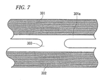
FIG. 7 .FIG. 7 illustrates the printedwiring board 201 according to the modification. Other components of theportable computer 100 are substantially similar to those illustrated inFIG. 1 . - The modification differs from the above embodiment in the shape of the
silk 301 a applied to the printedwiring board 201. In the modification, thesilk 301 a is applied to an area extending over theproduct part 301 and theend member 302 around the connectingpart 303. Such a shape of the appliedsilk 301 a increases an allowable degree of deviation of the mounting position of the printedwiring board 201 from the mountingsurface 351 of themold 350. That is, if the mounting position of the printedwiring board 201 deviates toward the inside of themold 350 when thepressing plate 352 is set or when a punching-cut operation is performed, an appropriate treatment will be performed. - Next, the
portable computer 100 serving as an electronic apparatus according to each of other embodiments is described hereinafter with reference toFIGS. 8 to 10 .FIG. 8 illustrates the printedwiring board 201 according to a second embodiment.FIG. 9 illustrates the printedwiring board 201 according to a third embodiment.FIG. 10 illustrates the printedwiring board 201 according to a fourth embodiment. Each component having functions which are the same as or similar to those of the associate component of theportable computer 100 according to the first embodiment is designated with the same reference numeral. Thus, the description of such components is omitted. The second to fourth embodiments differ from the first embodiment in the shape of the printedwiring board 201. Each of theportable computers 100 according to the second to fourth embodiments has an external appearance substantially the same as that illustrated inFIG. 1 . - The casing of each of the
portable computers 100 according to the second to fourth embodiments houses the printedwiring board 201. The printedwiring boards 201 according to the second to fourth embodiments are not subjected to routing to be performed before the punching-cut. In the printedwiring board 201 according to the second embodiment, hole-portions are provided on the punching orbit by drilling. In the printedwiring boards 201 according to the third and fourth embodiments, hole-portions or the like are not machined on the punching orbit. In the printedwiring board 201 according to the fourth embodiment, thesilk 301 a is discretely applied onto each product part. With such a configuration, advantages similar to those of the printed wiring board according to the first embodiment can be obtained. In addition, thesilk 301 a is more emphasized, so that the visual inspection is facilitated. - In the foregoing description, the first to fourth embodiments and the modification thereof have been described. However, the embodiments are not limited thereto. Components according to the first to third embodiments and the modifications thereof can be implemented by being appropriately combined with one another.
- The embodiments are applicable not only to a portable computer, but also to various electronic apparatuses, e.g., a hard disk drive, a digital camera, a digital video camera, and a personal digital assistant.
Claims (10)
1. A printed wiring board comprising:
a board body having a first surface and a second surface opposite thereto,
a product part defined in the board body, at which a wiring pattern is formed;
an end part defined in the board body, at a position separated from the product part;
a connecting part defined in the board body, through which the product part and the end part are connected; and
a coating-material applied on the first surface of the board body along the connecting part.
2. The printed wiring board of claim 1 ,
wherein the wiring pattern is provided at a position distant from the connecting part.
3. The printed wiring board of claim 2 ,
wherein the coating-material is applied to have a thickness the same with a height of the wiring pattern.
4. The printed wiring board of claim 3 ,
wherein the coating-material is provided by a silk-screen printing.
5. The printed wiring board of claim 4 ,
wherein the coating-material is provided on the second surface of the board body at the connecting part.
6. An electronic apparatus comprising:
a casing;
a board body to be housed in the casing, the board body having a first surface on which a wiring pattern is provided and a second surface opposite thereto;
a resist applied onto the first surface of the board body; and
a coating-material applied onto the resist along an edge part of the first surface of the board body.
7. The electronic apparatus of claim 6 ,
wherein the wiring pattern is provided at a position distant from the edge part.
8. The electronic apparatus of claim 7 ,
wherein the coating-material is applied to have a thickness the same with a height of the wiring pattern.
9. The electronic apparatus of claim 8 ,
wherein the coating-material is provided by a silk-screen printing.
10. The electronic apparatus of claim 9 ,
wherein the coating-material is provided on the resist on the second surface of the board body.
Applications Claiming Priority (2)
| Application Number | Priority Date | Filing Date | Title |
|---|---|---|---|
| JP2010084338A JP2011216717A (en) | 2010-03-31 | 2010-03-31 | Printed wiring board and electronic apparatus |
| JP2010-084338 | 2010-03-31 |
Publications (1)
| Publication Number | Publication Date |
|---|---|
| US20110240325A1 true US20110240325A1 (en) | 2011-10-06 |
Family
ID=44698043
Family Applications (1)
| Application Number | Title | Priority Date | Filing Date |
|---|---|---|---|
| US13/034,495 Abandoned US20110240325A1 (en) | 2010-03-31 | 2011-02-24 | Printed Wiring Board and Electronic Apparatus |
Country Status (3)
| Country | Link |
|---|---|
| US (1) | US20110240325A1 (en) |
| JP (1) | JP2011216717A (en) |
| CN (1) | CN102209430A (en) |
Cited By (2)
| Publication number | Priority date | Publication date | Assignee | Title |
|---|---|---|---|---|
| US20160161880A1 (en) * | 2014-12-08 | 2016-06-09 | Canon Kabushiki Kaisha | Printed circuit board, exposure device having printed circuit board, and image forming apparatus |
| TWI566930B (en) * | 2012-11-12 | 2017-01-21 | 松下知識產權經營股份有限公司 | Laminate, metal-clad laminate, printed wiring board, and multilayer printed wiring board |
Family Cites Families (6)
| Publication number | Priority date | Publication date | Assignee | Title |
|---|---|---|---|---|
| JPS6298795A (en) * | 1985-10-25 | 1987-05-08 | 日本シイエムケイ株式会社 | Printed wiring board and manufacture of the same |
| JP2791710B2 (en) * | 1990-06-22 | 1998-08-27 | 日本シイエムケイ株式会社 | Manufacturing method of printed wiring board |
| JP2868989B2 (en) * | 1993-12-27 | 1999-03-10 | ローム株式会社 | Component mounting method |
| JPH08148771A (en) * | 1994-11-18 | 1996-06-07 | Sanyo Electric Co Ltd | Divided printed circuit board |
| JP3890717B2 (en) * | 1998-01-14 | 2007-03-07 | 村田機械株式会社 | Printed circuit board |
| JP2002232085A (en) * | 2001-02-06 | 2002-08-16 | Sanken Electric Co Ltd | Circuit board mother board therefor, and manufacturing method thereof |
-
2010
- 2010-03-31 JP JP2010084338A patent/JP2011216717A/en active Pending
-
2011
- 2011-02-15 CN CN2011100430684A patent/CN102209430A/en active Pending
- 2011-02-24 US US13/034,495 patent/US20110240325A1/en not_active Abandoned
Cited By (3)
| Publication number | Priority date | Publication date | Assignee | Title |
|---|---|---|---|---|
| TWI566930B (en) * | 2012-11-12 | 2017-01-21 | 松下知識產權經營股份有限公司 | Laminate, metal-clad laminate, printed wiring board, and multilayer printed wiring board |
| US20160161880A1 (en) * | 2014-12-08 | 2016-06-09 | Canon Kabushiki Kaisha | Printed circuit board, exposure device having printed circuit board, and image forming apparatus |
| US9939753B2 (en) * | 2014-12-08 | 2018-04-10 | Canon Kabushiki Kaisha | Printed circuit board, exposure device having printed circuit board, and image forming apparatus |
Also Published As
| Publication number | Publication date |
|---|---|
| CN102209430A (en) | 2011-10-05 |
| JP2011216717A (en) | 2011-10-27 |
Similar Documents
| Publication | Publication Date | Title |
|---|---|---|
| KR100967135B1 (en) | Sheet metal member, information display device and panel unit manufacturing method | |
| US7158124B2 (en) | Touch panel including external connection terminal placed within outline of touch panel body provided with handle portion | |
| US10187984B1 (en) | Circuit board and method for making the same | |
| US20110240325A1 (en) | Printed Wiring Board and Electronic Apparatus | |
| US11083080B2 (en) | Virtual silk screen for printed circuit boards | |
| US20110254414A1 (en) | Computer enclosure having expansion card retention frame | |
| KR101131491B1 (en) | Sheet metal member, information display apparatus, and process for manufacturing panel unit | |
| KR100893343B1 (en) | Electronic apparatus | |
| US20090161327A1 (en) | Expansion card | |
| JPH11317570A (en) | Electronics | |
| JP2002289764A (en) | Flexible circuit board, display device and electronic device using the same | |
| US20090241335A1 (en) | Wiring work support device | |
| JP2005064058A (en) | Backup pin position determination device and backup pin position determination method | |
| US7768793B2 (en) | Multilayer printed wiring board, method of manufacturing multilayer printed wiring board and electronic apparatus | |
| JP2009290144A (en) | Electronics, printed circuit board, and method for producing printed circuit board | |
| JP2007165417A (en) | Flexible printed wiring board | |
| JP5280787B2 (en) | Electronic device and circuit board connection method | |
| JP4109589B2 (en) | Punching device | |
| CN217061304U (en) | TFT glass, display module assembly and electronic equipment | |
| JP2003289087A (en) | Wiring board, semiconductor device and manufacturing method thereof, panel module, and electronic device | |
| JP2010287670A (en) | Printed wiring boards and electronic devices | |
| JP2020092075A (en) | Module and substrate | |
| CN209823811U (en) | a mobile terminal | |
| JP2007243091A (en) | Electrical device and ground connecting structure | |
| KR102143106B1 (en) | Authentication module, manufacturing method thereof and protect cover for mobile terminal |
Legal Events
| Date | Code | Title | Description |
|---|---|---|---|
| AS | Assignment |
Owner name: KABUSHIKI KAISHA TOSHIBA, JAPAN Free format text: ASSIGNMENT OF ASSIGNORS INTEREST;ASSIGNORS:SUZUKI, DAIGO;KANOU, TERUNARI;SIGNING DATES FROM 20110202 TO 20110214;REEL/FRAME:025861/0180 |
|
| STCB | Information on status: application discontinuation |
Free format text: EXPRESSLY ABANDONED -- DURING EXAMINATION |