US20080098243A1 - Power-optimizing memory analyzer, method of operating the analyzer and system employing the same - Google Patents
Power-optimizing memory analyzer, method of operating the analyzer and system employing the same Download PDFInfo
- Publication number
- US20080098243A1 US20080098243A1 US11/853,674 US85367407A US2008098243A1 US 20080098243 A1 US20080098243 A1 US 20080098243A1 US 85367407 A US85367407 A US 85367407A US 2008098243 A1 US2008098243 A1 US 2008098243A1
- Authority
- US
- United States
- Prior art keywords
- memory
- power
- group
- task
- memory blocks
- Prior art date
- Legal status (The legal status is an assumption and is not a legal conclusion. Google has not performed a legal analysis and makes no representation as to the accuracy of the status listed.)
- Granted
Links
Images


Classifications
-
- G—PHYSICS
- G06—COMPUTING OR CALCULATING; COUNTING
- G06F—ELECTRIC DIGITAL DATA PROCESSING
- G06F1/00—Details not covered by groups G06F3/00 - G06F13/00 and G06F21/00
- G06F1/26—Power supply means, e.g. regulation thereof
- G06F1/32—Means for saving power
- G06F1/3203—Power management, i.e. event-based initiation of a power-saving mode
- G06F1/3234—Power saving characterised by the action undertaken
- G06F1/325—Power saving in peripheral device
- G06F1/3275—Power saving in memory, e.g. RAM, cache
-
- Y—GENERAL TAGGING OF NEW TECHNOLOGICAL DEVELOPMENTS; GENERAL TAGGING OF CROSS-SECTIONAL TECHNOLOGIES SPANNING OVER SEVERAL SECTIONS OF THE IPC; TECHNICAL SUBJECTS COVERED BY FORMER USPC CROSS-REFERENCE ART COLLECTIONS [XRACs] AND DIGESTS
- Y02—TECHNOLOGIES OR APPLICATIONS FOR MITIGATION OR ADAPTATION AGAINST CLIMATE CHANGE
- Y02D—CLIMATE CHANGE MITIGATION TECHNOLOGIES IN INFORMATION AND COMMUNICATION TECHNOLOGIES [ICT], I.E. INFORMATION AND COMMUNICATION TECHNOLOGIES AIMING AT THE REDUCTION OF THEIR OWN ENERGY USE
- Y02D10/00—Energy efficient computing, e.g. low power processors, power management or thermal management
-
- Y—GENERAL TAGGING OF NEW TECHNOLOGICAL DEVELOPMENTS; GENERAL TAGGING OF CROSS-SECTIONAL TECHNOLOGIES SPANNING OVER SEVERAL SECTIONS OF THE IPC; TECHNICAL SUBJECTS COVERED BY FORMER USPC CROSS-REFERENCE ART COLLECTIONS [XRACs] AND DIGESTS
- Y02—TECHNOLOGIES OR APPLICATIONS FOR MITIGATION OR ADAPTATION AGAINST CLIMATE CHANGE
- Y02D—CLIMATE CHANGE MITIGATION TECHNOLOGIES IN INFORMATION AND COMMUNICATION TECHNOLOGIES [ICT], I.E. INFORMATION AND COMMUNICATION TECHNOLOGIES AIMING AT THE REDUCTION OF THEIR OWN ENERGY USE
- Y02D30/00—Reducing energy consumption in communication networks
- Y02D30/50—Reducing energy consumption in communication networks in wire-line communication networks, e.g. low power modes or reduced link rate
Definitions
- the present disclosure is directed, in general, to memory systems and, more specifically, to a power-optimizing memory analyzer, a method of operating a power-optimizing memory analyzer and a memory system employing the analyzer or the method.
- CMOS circuits can play a dominant role in such devices, which are often integrated to the point of having a complete system on a chip (SoC).
- SoC system on a chip
- Embodiments of the present disclosure provide a power-optimizing memory analyzer, a method of operating a power-optimizing memory analyzer and a memory system employing the analyzer or the method.
- the power-optimizing memory analyzer is for use with an array of memory blocks and includes a task database configured to provide a parameter set corresponding to each of a set of tasks to be performed in a system.
- the power-optimizing memory analyzer also includes an allocation module configured to determine offline, a group of memory blocks in the array corresponding to the parameter set for each task and based on a power reduction for the array.
- the method includes providing a parameter set corresponding to each of a set of tasks to be performed in a system and determining offline, a group of memory blocks in an array corresponding to the parameter set for each task and based on a power reduction for the array.
- the memory system includes an array of memory blocks, a run-time power controller and applications and operating system software, which are coupled to the array of memory blocks and the run-time power controller that correspond to a set of tasks to be performed.
- the memory system also includes a power-optimizing memory analyzer having a task database that provides a parameter set corresponding to each of the set of tasks.
- the power-optimizing memory analyzer also has an allocation module that determines offline a group of memory blocks in the array, corresponding to the parameter set for each task and based on a power reduction for the array of memory blocks.
- the power-optimizing memory analyzer further has a power profiling module that generates a run-time power profile of memory power states for coordination with the run-time power controller in scheduling each group of memory blocks during run time, based on maintaining a quality of service for the system.
- FIG. 1 illustrates a block diagram of a memory system as provided by one embodiment of the disclosure
- FIG. 2 illustrates a diagram of memory power states as provided by one embodiment of the disclosure
- FIGS. 3A and 3B respectively illustrate a traditional memory layout organization and a power-efficient, task-based memory layout organization as may be selected by an allocation module;
- FIG. 4 illustrates a diagram of a run-time operation employing power profiling
- FIG. 5 illustrates a flow diagram of an embodiment of a method of operating a power-optimizing memory analyzer carried out in accordance with the principles of the present disclosure.
- Embodiments of the present disclosure provide a collaborated and systematic approach that organizes memory layout and controls memory power states to conserve memory power. This is accomplished both transparently and dynamically with a focus on maintaining quality of service for a system.
- the task-based approach of memory management employed in the embodiments illustrated below addresses current issues. For example, single large memory blocks typically result in generally higher memory access power, while a multiplicity of memory blocks often results in standby power that dramatically increases at elevated ambient temperatures. Putting memory into retention reduces system performance due to overhead time needed to achieve activation. Having to power down memory may break system integrity due to lost content.
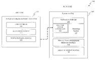
- FIG. 1 illustrates a block diagram of a memory system 100 as provided by one embodiment of the disclosure.
- the illustrated embodiment of the memory system 100 includes a System on a Chip (SoC) 105 , which is a run-time portion and a power-optimizing memory analyzer 115 , which is an off-line portion.
- SoC 105 includes applications software 106 , operating system software 107 , a memory power management hardware interface 108 and an array of memory blocks 109 .
- the SoC 105 also includes a run-time power controller 120 that utilizes information from run-time power profiles that are generated by the power-optimizing memory analyzer 115 .
- the power-optimizing memory analyzer 115 includes a task database 116 , an allocation module 117 and a power profiling module 118 .
- the applications and operating system software 106 , 107 orchestrate a set of tasks that are accomplished by the SoC 105 in delivering a collection of features and functions.
- the run-time power controller 120 is coupled to the memory power management hardware interface 108 and the operating system software 107 to provide control of the array of memory blocks 109 corresponding to the set of tasks.
- the task database 116 provides a parameter set corresponding to each of the set of tasks.
- the parameter set typically includes a plurality of parameters needed by the allocation module 117 .
- a memory block specification for each type of memory block that is used by the Soc 105 is included.
- the various power requirements and response times associated with each type of memory block are included.
- the overhead time needed to switch between various memory power states is employed.
- the parameter set includes application memory map files and software objects associated with each task.
- the allocation module 117 provides an offline determination of a group of memory blocks in the array of memory blocks 109 corresponding to the parameter set for each task. Selection of this particular group of memory blocks is based on providing a power reduction that may be achieved for the array. In making the determination, the allocation module 117 analyzes the period of time that each task is going to run, and what types of memory are required while the task is running. This is based on the application memory map files and software objects associated with each task. Additionally, a determination is made as to the amount of time spent reading from and writing to a memory block for each task.
- the allocation module 117 provides a memory power savings by reducing the number of memory blocks needed for a task by grouping like software objects for each task.
- FIG. 2 illustrates a diagram of memory power states 200 as provided by one embodiment of the disclosure.
- the memory power states 200 include an access mode 205 , a standby mode 207 , a retention mode 209 and a power down mode 211 for the group of memory blocks determined by an allocation module such as the allocation module of FIG. 1 .
- the access mode 205 provides full power to a memory block and is needed to read from and write to the memory block at full performance speeds.
- the standby mode 207 provides a power savings over the access mode while the memory block is not being accessed.
- a power level for the standby mode 207 is determined such that the access mode 205 may be provided transparently to the processing of a task that needs memory block access. Therefore, the power savings afforded by the standby mode 207 is usually small, although not negligible.
- the combination of the access and standby modes 205 , 207 working together is called an active mode of the memory block, since there is an automatic transitioning from the standby mode 207 to the access mode 205 when access is required.
- the retention mode 209 provides a memory block power level that only allows retaining memory states for the memory block thereby providing even greater power savings. Moving from the retention mode 209 requires a longer transition time than from the standby mode 207 to the access mode 205 . Consequently, transitioning from the retention mode 209 to the access mode 205 requires an even longer transition time.
- the power down mode 211 removes all power from the memory block and provides maximum power savings. Transitioning to the retention, standby or access modes 209 , 207 , and 205 requires increasingly longer transition times.
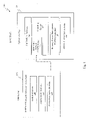
- FIGS. 3A and 3B respectively illustrate a traditional memory layout organization 300 and a power-efficient, task-based memory layout organization 350 as may be selected by an allocation module such as the one discussed in FIG. 1 .
- a portion of the estimated power savings determined by the allocation module corresponds to a grouping of like software objects for each task in the group of memory blocks.
- the memory layout organization 300 includes a collection of seven memory blocks 305 having a collection of software objects corresponding to a task 1 , as shown.
- the memory blocks 305 correspond to three different memory usages (i.e., .text, .data and .bss).
- Task 1 is required to access the software objects A and E, thereby requiring six of the seven memory blocks to be accessed.
- the memory layout organization 300 is typical of one where memory power is not an issue and constantly resides at the access mode level.
- the memory layout organization 350 also includes a collection of seven memory blocks 305 having a collection of software objects corresponding to the task 1 , as shown. However, the task-based memory layout organization 350 places the required software objects A and E into only a group of three of the seven memory blocks. This allows four of the seven memory blocks to be placed in either the retention or power down modes as described in FIG. 2 , thereby providing a power savings. Additionally, the three active mode memory blocks containing the software objects A and E may also provide a power savings in the standby mode until they are being accessed.
- the allocation module 117 employs knowledge of the various memory power states and transition times as well as the task-based memory layout organizations to provide a schedulability analysis of the group of memory blocks corresponding to run-time constraints.
- the power profiling module 118 then generates the run-time power profile of memory allocations and power states for coordination with the applications and operating system softwares 106 , 107 by means of the run-time power controller 120 .
- the run-time power controller 120 is employed in scheduling each group of memory blocks during run time, based on maintaining a quality of service for the Soc 105 .
- a change in memory power states for the group of memory modules occurs at context switching of a task.
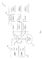
- FIG. 4 illustrates a diagram of a run-time operation 400 employing power profiling.
- the run-time operation 400 includes a memory array 405 , first and second applications 410 a , 410 b , operating software 415 and a run-time power profile 420 .
- the memory array 405 includes a collection of memory blocks MEM 11 -MEM 33 .
- the columns of memory blocks correspond to three different types of memory, and the rows correspond to three different memory usages, as was shown in FIGS. 3A and 3B .
- Task 2 of the first application 410 a is currently running and requires a group of memory blocks MEM 11 , MEM 13 , MEM 22 , as shown. These memory blocks contain the software objects required to run task 2 and reflect the type of task-based memory layout organization discussed with respect to FIG. 33 . This memory layout is dictated by the run-time power profile 420 for task 2 of the first application 410 a .
- the group of memory blocks MEM 11 , MEM 13 , MEM 22 has been placed in the active power state while the power state of the remaining memory blocks is either in the retention mode or the power down mode.
- the operating system 415 in corporation with the direction of the run-time power profile 420 , will select another group of memory blocks and appropriate power levels for the next task to run based on its run-time power profile.
- FIG. 5 illustrates a flow diagram of an embodiment of a method 500 of operating a power-optimizing memory analyzer carried out in accordance with the principles of the present disclosure.
- the method 500 starts in a step 505 and is for use with an array of memory blocks.
- a parameter set corresponding to each of a set of tasks to be performed in a system is provided.
- the parameter set includes, for example, memory block specifications wherein the specifications provide overhead times needed to power up each of the types of memory blocks that may be employed.
- the parameter set also includes application memory map files as well as software objects associated with each task.
- a group of memory blocks in the array corresponding to the parameter set for each task is determined offline.
- the selection of the group of memory blocks is based on providing a power reduction for the array of memory blocks that may be achieved when the group is employed in accomplishing the task.
- a portion of the estimated power saving corresponds to selecting memory power states for the group of memory blocks.
- the memory power states correspond to an access mode, a standby mode, a retention mode and a power down mode of operating the group of memory blocks.
- a portion of the estimated power savings corresponds to a grouping of like software objects for each task in the group of memory blocks.
- a schedulability analysis of the group of memory blocks corresponding to run-time constraints of the system is also determined in the step 515 .
- This schedulability analysis is employed in a step 520 to generate a run-time power profile of memory power states.
- the run-time power profile coordinates with existing run-time software in scheduling each group of memory blocks based on maintaining a quality of service for the system.
- a change in memory power states for the group of memory blocks occurs at context switching of a task.
- the method 500 ends in a step 525 .
Landscapes
- Engineering & Computer Science (AREA)
- Theoretical Computer Science (AREA)
- Physics & Mathematics (AREA)
- General Engineering & Computer Science (AREA)
- General Physics & Mathematics (AREA)
- Techniques For Improving Reliability Of Storages (AREA)
- Power Sources (AREA)
Abstract
Description
- This application claims the benefit of U.S. Provisional Application No. 60/825,235 entitled “System-on-Chip Task Scheduling That Dynamically Selects The Optimal Combination MEM Power Management Techniques Based on Task Memory Profiling Data” to Saowanee Saewong and Xiaolin Lu, filed on Sep. 11, 2006, which is incorporated herein by reference in its entirety.
- The present disclosure is directed, in general, to memory systems and, more specifically, to a power-optimizing memory analyzer, a method of operating a power-optimizing memory analyzer and a memory system employing the analyzer or the method.
- A major trend, especially in portable electronic devices, is towards smaller physical sizes using wireless communications and multimedia processing. This situation typically requires increased computing power to supply the feature-rich functionality needed. CMOS circuits can play a dominant role in such devices, which are often integrated to the point of having a complete system on a chip (SoC). These SoC-based devices are growing in complexity and speed requirements while at the same time shrinking in physical size thereby generating increased reliability issues. Although current devices are providing reliable operation, further improvements would prove beneficial in the art.
- Embodiments of the present disclosure provide a power-optimizing memory analyzer, a method of operating a power-optimizing memory analyzer and a memory system employing the analyzer or the method. In one embodiment, the power-optimizing memory analyzer is for use with an array of memory blocks and includes a task database configured to provide a parameter set corresponding to each of a set of tasks to be performed in a system. The power-optimizing memory analyzer also includes an allocation module configured to determine offline, a group of memory blocks in the array corresponding to the parameter set for each task and based on a power reduction for the array.
- In another aspect, the method includes providing a parameter set corresponding to each of a set of tasks to be performed in a system and determining offline, a group of memory blocks in an array corresponding to the parameter set for each task and based on a power reduction for the array.
- The memory system includes an array of memory blocks, a run-time power controller and applications and operating system software, which are coupled to the array of memory blocks and the run-time power controller that correspond to a set of tasks to be performed. The memory system also includes a power-optimizing memory analyzer having a task database that provides a parameter set corresponding to each of the set of tasks. The power-optimizing memory analyzer also has an allocation module that determines offline a group of memory blocks in the array, corresponding to the parameter set for each task and based on a power reduction for the array of memory blocks. The power-optimizing memory analyzer further has a power profiling module that generates a run-time power profile of memory power states for coordination with the run-time power controller in scheduling each group of memory blocks during run time, based on maintaining a quality of service for the system.
- The foregoing has outlined preferred and alternative features of the present disclosure so that those skilled in the art may better understand the detailed description of the disclosure that follows. Additional features of the disclosure will be described hereinafter that form the subject of the claims of the disclosure. Those skilled in the art will appreciate that they can readily use the disclosed conception and specific embodiment as a basis for designing or modifying other structures for carrying out the same purposes of the present disclosure.
- For a more complete understanding of the present disclosure, reference is now made to the following descriptions taken in conjunction with the accompanying drawings, in which:
-
FIG. 1 illustrates a block diagram of a memory system as provided by one embodiment of the disclosure; -
FIG. 2 illustrates a diagram of memory power states as provided by one embodiment of the disclosure; -
FIGS. 3A and 3B respectively illustrate a traditional memory layout organization and a power-efficient, task-based memory layout organization as may be selected by an allocation module; -
FIG. 4 illustrates a diagram of a run-time operation employing power profiling; and -
FIG. 5 illustrates a flow diagram of an embodiment of a method of operating a power-optimizing memory analyzer carried out in accordance with the principles of the present disclosure. - Embodiments of the present disclosure provide a collaborated and systematic approach that organizes memory layout and controls memory power states to conserve memory power. This is accomplished both transparently and dynamically with a focus on maintaining quality of service for a system. The task-based approach of memory management employed in the embodiments illustrated below addresses current issues. For example, single large memory blocks typically result in generally higher memory access power, while a multiplicity of memory blocks often results in standby power that dramatically increases at elevated ambient temperatures. Putting memory into retention reduces system performance due to overhead time needed to achieve activation. Having to power down memory may break system integrity due to lost content.
-
FIG. 1 illustrates a block diagram of amemory system 100 as provided by one embodiment of the disclosure. The illustrated embodiment of thememory system 100 includes a System on a Chip (SoC) 105, which is a run-time portion and a power-optimizingmemory analyzer 115, which is an off-line portion. The SoC 105 includesapplications software 106,operating system software 107, a memory powermanagement hardware interface 108 and an array ofmemory blocks 109. The SoC 105 also includes a run-time power controller 120 that utilizes information from run-time power profiles that are generated by the power-optimizingmemory analyzer 115. The power-optimizingmemory analyzer 115 includes atask database 116, anallocation module 117 and apower profiling module 118. - The applications and
operating system software time power controller 120 is coupled to the memory powermanagement hardware interface 108 and theoperating system software 107 to provide control of the array ofmemory blocks 109 corresponding to the set of tasks. - The
task database 116 provides a parameter set corresponding to each of the set of tasks. The parameter set typically includes a plurality of parameters needed by theallocation module 117. For example, a memory block specification for each type of memory block that is used by the Soc 105 is included. Of interest are the various power requirements and response times associated with each type of memory block. Of particular interest is the overhead time needed to switch between various memory power states that may be employed. Additionally, the parameter set includes application memory map files and software objects associated with each task. - The
allocation module 117 provides an offline determination of a group of memory blocks in the array ofmemory blocks 109 corresponding to the parameter set for each task. Selection of this particular group of memory blocks is based on providing a power reduction that may be achieved for the array. In making the determination, theallocation module 117 analyzes the period of time that each task is going to run, and what types of memory are required while the task is running. This is based on the application memory map files and software objects associated with each task. Additionally, a determination is made as to the amount of time spent reading from and writing to a memory block for each task. - These are key parameters for the
allocation module 117 in determining memory power states and overall power estimations for each of the types of memory blocks used by the set of tasks. Additionally, theallocation module 117 provides a memory power savings by reducing the number of memory blocks needed for a task by grouping like software objects for each task. -
FIG. 2 illustrates a diagram ofmemory power states 200 as provided by one embodiment of the disclosure. Thememory power states 200 include anaccess mode 205, astandby mode 207, aretention mode 209 and a power downmode 211 for the group of memory blocks determined by an allocation module such as the allocation module ofFIG. 1 . Theaccess mode 205 provides full power to a memory block and is needed to read from and write to the memory block at full performance speeds. - The
standby mode 207 provides a power savings over the access mode while the memory block is not being accessed. A power level for thestandby mode 207 is determined such that theaccess mode 205 may be provided transparently to the processing of a task that needs memory block access. Therefore, the power savings afforded by thestandby mode 207 is usually small, although not negligible. The combination of the access andstandby modes standby mode 207 to theaccess mode 205 when access is required. - The
retention mode 209 provides a memory block power level that only allows retaining memory states for the memory block thereby providing even greater power savings. Moving from theretention mode 209 requires a longer transition time than from thestandby mode 207 to theaccess mode 205. Consequently, transitioning from theretention mode 209 to theaccess mode 205 requires an even longer transition time. The power downmode 211 removes all power from the memory block and provides maximum power savings. Transitioning to the retention, standby oraccess modes -
FIGS. 3A and 3B respectively illustrate a traditionalmemory layout organization 300 and a power-efficient, task-basedmemory layout organization 350 as may be selected by an allocation module such as the one discussed inFIG. 1 . A portion of the estimated power savings determined by the allocation module corresponds to a grouping of like software objects for each task in the group of memory blocks. - The
memory layout organization 300 includes a collection of sevenmemory blocks 305 having a collection of software objects corresponding to atask 1, as shown. The memory blocks 305 correspond to three different memory usages (i.e., .text, .data and .bss).Task 1 is required to access the software objects A and E, thereby requiring six of the seven memory blocks to be accessed. Thememory layout organization 300 is typical of one where memory power is not an issue and constantly resides at the access mode level. - The
memory layout organization 350 also includes a collection of sevenmemory blocks 305 having a collection of software objects corresponding to thetask 1, as shown. However, the task-basedmemory layout organization 350 places the required software objects A and E into only a group of three of the seven memory blocks. This allows four of the seven memory blocks to be placed in either the retention or power down modes as described inFIG. 2 , thereby providing a power savings. Additionally, the three active mode memory blocks containing the software objects A and E may also provide a power savings in the standby mode until they are being accessed. - Returning to
FIG. 1 , theallocation module 117 employs knowledge of the various memory power states and transition times as well as the task-based memory layout organizations to provide a schedulability analysis of the group of memory blocks corresponding to run-time constraints. Thepower profiling module 118 then generates the run-time power profile of memory allocations and power states for coordination with the applications and operating system softwares 106, 107 by means of the run-time power controller 120. The run-time power controller 120 is employed in scheduling each group of memory blocks during run time, based on maintaining a quality of service for theSoc 105. In the illustrated embodiment, a change in memory power states for the group of memory modules occurs at context switching of a task. -
FIG. 4 illustrates a diagram of a run-time operation 400 employing power profiling. The run-time operation 400 includes amemory array 405, first andsecond applications operating software 415 and a run-time power profile 420. Thememory array 405 includes a collection of memory blocks MEM11-MEM33. The columns of memory blocks correspond to three different types of memory, and the rows correspond to three different memory usages, as was shown inFIGS. 3A and 3B . -
Task 2 of thefirst application 410 a is currently running and requires a group of memory blocks MEM11, MEM13, MEM22, as shown. These memory blocks contain the software objects required to runtask 2 and reflect the type of task-based memory layout organization discussed with respect toFIG. 33 . This memory layout is dictated by the run-time power profile 420 fortask 2 of thefirst application 410 a. The group of memory blocks MEM11, MEM13, MEM22 has been placed in the active power state while the power state of the remaining memory blocks is either in the retention mode or the power down mode. At the completion oftask 2 of thefirst application 410 a, theoperating system 415, in corporation with the direction of the run-time power profile 420, will select another group of memory blocks and appropriate power levels for the next task to run based on its run-time power profile. -
FIG. 5 illustrates a flow diagram of an embodiment of amethod 500 of operating a power-optimizing memory analyzer carried out in accordance with the principles of the present disclosure. Themethod 500 starts in astep 505 and is for use with an array of memory blocks. Then, in astep 510, a parameter set corresponding to each of a set of tasks to be performed in a system is provided. The parameter set includes, for example, memory block specifications wherein the specifications provide overhead times needed to power up each of the types of memory blocks that may be employed. The parameter set also includes application memory map files as well as software objects associated with each task. - A group of memory blocks in the array corresponding to the parameter set for each task is determined offline. The selection of the group of memory blocks is based on providing a power reduction for the array of memory blocks that may be achieved when the group is employed in accomplishing the task. A portion of the estimated power saving corresponds to selecting memory power states for the group of memory blocks. In one embodiment, the memory power states correspond to an access mode, a standby mode, a retention mode and a power down mode of operating the group of memory blocks. Additionally, a portion of the estimated power savings corresponds to a grouping of like software objects for each task in the group of memory blocks. A schedulability analysis of the group of memory blocks corresponding to run-time constraints of the system is also determined in the
step 515. - This schedulability analysis is employed in a
step 520 to generate a run-time power profile of memory power states. The run-time power profile coordinates with existing run-time software in scheduling each group of memory blocks based on maintaining a quality of service for the system. A change in memory power states for the group of memory blocks occurs at context switching of a task. Themethod 500 ends in astep 525. - While the method disclosed herein has been described and shown with reference to particular steps performed in a particular order, it will be understood that these steps may be combined, subdivided, or reordered to form an equivalent method without departing from the teachings of the present disclosure. Accordingly, unless specifically indicated herein, the order or the grouping of the steps is not a limitation of the present disclosure.
- Those skilled in the art to which the disclosure relates will appreciate that other and further additions, deletions, substitutions and modifications may be made to the described example embodiments without departing from the disclosure.
Claims (20)
Priority Applications (1)
| Application Number | Priority Date | Filing Date | Title |
|---|---|---|---|
| US11/853,674 US7930565B2 (en) | 2006-09-11 | 2007-09-11 | Power-optimizing memory analyzer, method of operating the analyzer and system employing the same |
Applications Claiming Priority (2)
| Application Number | Priority Date | Filing Date | Title |
|---|---|---|---|
| US82523506P | 2006-09-11 | 2006-09-11 | |
| US11/853,674 US7930565B2 (en) | 2006-09-11 | 2007-09-11 | Power-optimizing memory analyzer, method of operating the analyzer and system employing the same |
Publications (2)
| Publication Number | Publication Date |
|---|---|
| US20080098243A1 true US20080098243A1 (en) | 2008-04-24 |
| US7930565B2 US7930565B2 (en) | 2011-04-19 |
Family
ID=39319465
Family Applications (1)
| Application Number | Title | Priority Date | Filing Date |
|---|---|---|---|
| US11/853,674 Active 2029-10-08 US7930565B2 (en) | 2006-09-11 | 2007-09-11 | Power-optimizing memory analyzer, method of operating the analyzer and system employing the same |
Country Status (1)
| Country | Link |
|---|---|
| US (1) | US7930565B2 (en) |
Cited By (7)
| Publication number | Priority date | Publication date | Assignee | Title |
|---|---|---|---|---|
| US20100070695A1 (en) * | 2008-09-15 | 2010-03-18 | Texas Instruments Incorporated | Power-efficient memory management for embedded systems |
| WO2012107798A1 (en) * | 2011-02-08 | 2012-08-16 | Freescale Semiconductor, Inc. | Integrated circuit device, power management module and method for providing power management |
| TWI407303B (en) * | 2009-03-30 | 2013-09-01 | Mediatek Inc | Method for reducing power consumption and device with an embedded memory module |
| EP2889719A1 (en) * | 2013-12-23 | 2015-07-01 | Intel IP Corporation | Method and apparatus to manage power usage in a processor |
| US9311228B2 (en) | 2012-04-04 | 2016-04-12 | International Business Machines Corporation | Power reduction in server memory system |
| US9665155B2 (en) | 2013-12-28 | 2017-05-30 | Intel Corporation | Techniques for increasing energy efficiency of sensor controllers that receive data from one or more sensors |
| WO2018208354A1 (en) * | 2017-05-08 | 2018-11-15 | Qualcomm Incorporated | Configurable low memory modes for reduced power consumption |
Families Citing this family (4)
| Publication number | Priority date | Publication date | Assignee | Title |
|---|---|---|---|---|
| RU2012127578A (en) * | 2012-07-02 | 2014-01-10 | ЭлЭсАй Корпорейшн | ANALYZER OF APPLICABILITY OF THE SOFTWARE MODULE FOR THE DEVELOPMENT AND TESTING OF THE SOFTWARE FOR MULTIPROCESSOR MEDIA |
| US9323574B2 (en) * | 2014-02-21 | 2016-04-26 | Lenovo Enterprise Solutions (Singapore) Pte. Ltd. | Processor power optimization with response time assurance |
| US9690364B2 (en) * | 2015-09-04 | 2017-06-27 | Qualcomm Incorporated | Systems and methods for dynamically adjusting memory state transition timers |
| US10539997B2 (en) | 2016-09-02 | 2020-01-21 | Qualcomm Incorporated | Ultra-low-power design memory power reduction scheme |
Citations (5)
| Publication number | Priority date | Publication date | Assignee | Title |
|---|---|---|---|---|
| US5148546A (en) * | 1991-04-22 | 1992-09-15 | Blodgett Greg A | Method and system for minimizing power demands on portable computers and the like by refreshing selected dram cells |
| US6751739B1 (en) * | 2000-01-17 | 2004-06-15 | Gary J. Verdun | System and method for adjusting a memory pool configuration by assessing task performance of a specified application |
| US7206960B2 (en) * | 2003-08-22 | 2007-04-17 | Hewlett-Packard Development Company, L.P. | Bus clock frequency management based on device load |
| US7454639B2 (en) * | 2005-06-30 | 2008-11-18 | Intel Corporation | Various apparatuses and methods for reduced power states in system memory |
| US7539994B2 (en) * | 2003-01-03 | 2009-05-26 | Intel Corporation | Dynamic performance and resource management in a processing system |
-
2007
- 2007-09-11 US US11/853,674 patent/US7930565B2/en active Active
Patent Citations (5)
| Publication number | Priority date | Publication date | Assignee | Title |
|---|---|---|---|---|
| US5148546A (en) * | 1991-04-22 | 1992-09-15 | Blodgett Greg A | Method and system for minimizing power demands on portable computers and the like by refreshing selected dram cells |
| US6751739B1 (en) * | 2000-01-17 | 2004-06-15 | Gary J. Verdun | System and method for adjusting a memory pool configuration by assessing task performance of a specified application |
| US7539994B2 (en) * | 2003-01-03 | 2009-05-26 | Intel Corporation | Dynamic performance and resource management in a processing system |
| US7206960B2 (en) * | 2003-08-22 | 2007-04-17 | Hewlett-Packard Development Company, L.P. | Bus clock frequency management based on device load |
| US7454639B2 (en) * | 2005-06-30 | 2008-11-18 | Intel Corporation | Various apparatuses and methods for reduced power states in system memory |
Cited By (12)
| Publication number | Priority date | Publication date | Assignee | Title |
|---|---|---|---|---|
| US20100070695A1 (en) * | 2008-09-15 | 2010-03-18 | Texas Instruments Incorporated | Power-efficient memory management for embedded systems |
| US8478932B2 (en) * | 2008-09-15 | 2013-07-02 | Texas Instruments Incorporated | Power efficient memory management for embedded systems |
| TWI407303B (en) * | 2009-03-30 | 2013-09-01 | Mediatek Inc | Method for reducing power consumption and device with an embedded memory module |
| WO2012107798A1 (en) * | 2011-02-08 | 2012-08-16 | Freescale Semiconductor, Inc. | Integrated circuit device, power management module and method for providing power management |
| CN103348303A (en) * | 2011-02-08 | 2013-10-09 | 飞思卡尔半导体公司 | Integrated circuit device, power management module and method for providing power management |
| US9368162B2 (en) | 2011-02-08 | 2016-06-14 | Freescale Semiconductor, Inc. | Integrated circuit device, power management module and method for providing power management |
| US9311228B2 (en) | 2012-04-04 | 2016-04-12 | International Business Machines Corporation | Power reduction in server memory system |
| EP2889719A1 (en) * | 2013-12-23 | 2015-07-01 | Intel IP Corporation | Method and apparatus to manage power usage in a processor |
| US9836113B2 (en) | 2013-12-23 | 2017-12-05 | Intel Corporation | Method and apparatus to manage power usage in a processor |
| US9665155B2 (en) | 2013-12-28 | 2017-05-30 | Intel Corporation | Techniques for increasing energy efficiency of sensor controllers that receive data from one or more sensors |
| WO2018208354A1 (en) * | 2017-05-08 | 2018-11-15 | Qualcomm Incorporated | Configurable low memory modes for reduced power consumption |
| US10409513B2 (en) | 2017-05-08 | 2019-09-10 | Qualcomm Incorporated | Configurable low memory modes for reduced power consumption |
Also Published As
| Publication number | Publication date |
|---|---|
| US7930565B2 (en) | 2011-04-19 |
Similar Documents
| Publication | Publication Date | Title |
|---|---|---|
| US7930565B2 (en) | Power-optimizing memory analyzer, method of operating the analyzer and system employing the same | |
| US20230185355A1 (en) | Discrete power control of components within a computer system | |
| US7783905B2 (en) | Method for reducing power consumption of a computer system in the working state | |
| KR101053010B1 (en) | Managing power on integrated circuits using power islands | |
| US5826092A (en) | Method and apparatus for performance optimization in power-managed computer systems | |
| US9377830B2 (en) | Data processing device with power management unit and portable device having the same | |
| US8479031B2 (en) | System switching unit having a switch to switch on/off a channel for data interaction between a first system and the bus interface of a second system according to the operation state of the second system | |
| US20110047316A1 (en) | Solid state memory device power optimization | |
| US20080313482A1 (en) | Power Partitioning Memory Banks | |
| KR20130002046A (en) | Power management method for storage device including multi-core | |
| CN1574999B (en) | Information processing device | |
| TWI224728B (en) | Method and related apparatus for maintaining stored data of a dynamic random access memory | |
| JP2014157508A (en) | Arithmetic device, array type arithmetic device and control method thereof, and information processing system | |
| US20220171551A1 (en) | Available memory optimization to manage multiple memory channels | |
| CN102203746A (en) | Combined mobile device and solid state disk with a shared memory architecture | |
| US7992015B2 (en) | Processor performance state optimization | |
| JP2005235223A (en) | Low power integrated circuit device by dynamic voltage scaling | |
| JP2011048550A (en) | Method and program for memory relocation control of computer, and computer system | |
| KR100806284B1 (en) | High Energy Efficiency Processor Using Dynamic Voltage Scaling | |
| US7685444B2 (en) | Power saving in circuit functions through multiple power buses | |
| CN109375543B (en) | DVS voltage management device, DVS voltage management system, DVS voltage management method, storage medium, and computer device | |
| CN101655734B (en) | Computer with power-saving state control and its control method | |
| US20060230304A1 (en) | Frequency control method and information processing apparatus | |
| CN113986001A (en) | Chip and control method | |
| US20060064606A1 (en) | A method and apparatus for controlling power consumption in an integrated circuit |
Legal Events
| Date | Code | Title | Description |
|---|---|---|---|
| AS | Assignment |
Owner name: TEXAS INSTRUMENTS INC., TEXAS Free format text: ASSIGNMENT OF ASSIGNORS INTEREST;ASSIGNORS:SAEWONG, SAOWANEE;LU, XIAOLIN;REEL/FRAME:019813/0922 Effective date: 20070911 |
|
| STCF | Information on status: patent grant |
Free format text: PATENTED CASE |
|
| FPAY | Fee payment |
Year of fee payment: 4 |
|
| MAFP | Maintenance fee payment |
Free format text: PAYMENT OF MAINTENANCE FEE, 8TH YEAR, LARGE ENTITY (ORIGINAL EVENT CODE: M1552); ENTITY STATUS OF PATENT OWNER: LARGE ENTITY Year of fee payment: 8 |
|
| MAFP | Maintenance fee payment |
Free format text: PAYMENT OF MAINTENANCE FEE, 12TH YEAR, LARGE ENTITY (ORIGINAL EVENT CODE: M1553); ENTITY STATUS OF PATENT OWNER: LARGE ENTITY Year of fee payment: 12 |