US20080098140A1 - Access control device and access control method - Google Patents
Access control device and access control method Download PDFInfo
- Publication number
- US20080098140A1 US20080098140A1 US11/876,044 US87604407A US2008098140A1 US 20080098140 A1 US20080098140 A1 US 20080098140A1 US 87604407 A US87604407 A US 87604407A US 2008098140 A1 US2008098140 A1 US 2008098140A1
- Authority
- US
- United States
- Prior art keywords
- start signal
- transaction start
- address
- signal
- pci
- Prior art date
- Legal status (The legal status is an assumption and is not a legal conclusion. Google has not performed a legal analysis and makes no representation as to the accuracy of the status listed.)
- Granted
Links
Images


Classifications
-
- G—PHYSICS
- G06—COMPUTING OR CALCULATING; COUNTING
- G06F—ELECTRIC DIGITAL DATA PROCESSING
- G06F13/00—Interconnection of, or transfer of information or other signals between, memories, input/output devices or central processing units
- G06F13/14—Handling requests for interconnection or transfer
-
- G—PHYSICS
- G06—COMPUTING OR CALCULATING; COUNTING
- G06F—ELECTRIC DIGITAL DATA PROCESSING
- G06F13/00—Interconnection of, or transfer of information or other signals between, memories, input/output devices or central processing units
- G06F13/38—Information transfer, e.g. on bus
- G06F13/40—Bus structure
- G06F13/4004—Coupling between buses
- G06F13/4027—Coupling between buses using bus bridges
-
- G—PHYSICS
- G06—COMPUTING OR CALCULATING; COUNTING
- G06F—ELECTRIC DIGITAL DATA PROCESSING
- G06F13/00—Interconnection of, or transfer of information or other signals between, memories, input/output devices or central processing units
Definitions
- the present invention relates to an access control device and an access control method.
- PCI Peripheral Component Interconnect
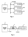
- the PCI bus can connect to a plurality of PCI devices. For example, as shown in FIG. 4 , a PCI host control unit 1 and a plurality of PCI devices 2 A- 2 C connect to a PCI bus 3 .
- a CardBus As a standard of a bus used for a PC card, a CardBus is known.
- the CardBus is configured based on a PCI.
- signal specifications of the PCI bus and the CardBus are not perfectly identical. Therefore, a device 4 based upon the CardBus standard (hereinafter, referred to as a CardBus device) such as the PC card cannot be connected to the PCI bus directly. Accordingly, for example, as shown in FIG. 5 , if the CardBus device 4 and the PCI host control unit 1 are connected, a PCI-CardBus bridge 5 has to be interposed therebetween.
- the PCI-CardBus bridge 5 is large-sized and costly. Only one CardBus device can be connected to one PCI-CardBus bridge 5 .
- the PCI host control unit 1 accesses the PCI devices 2 A- 2 C via the PCI bus 3 .
- the PCI host control unit 1 performs configuration processing.
- a PCI includes an address space of 4 G bytes.
- an access region of each PCI devices 2 A- 2 B is assigned to one of areas in the address space with 4 G bytes.
- the access region of the PCI device 2 A is assigned to 0x10000000-0x1000FFFF (0x: a hexadecimal number), and the access region of the PCI device 2 B is assigned to 0x10010000-0x10010FFF, and the access region of the PCI device 2 C is assigned to 0x20000000-0x20007FFF.
- Information concerning the access region of each PCI devices 2 A- 2 C is stored in a configuration register.
- the PCI host control unit 1 reads a value of the configuration register of each PCI devices 2 A- 2 C.
- PCI devices 2 A- 2 C can distinguish whether predetermined access is an access addressed to itself as an address on the PCI. Accordingly, even when a plurality of PCI devices 2 A- 2 C are connected to a PCI bus 3 , signals of the devices does not conflict.
- a PCI includes an IDSEL signal which is effective only during the configuration processing.
- the IDSEL signal is a signal showing a configuration register of a device to be accessed. The IDSEL signal avoids an access conflict between the PCI devices 2 A- 2 C during the configuration processing.
- Japanese Patent Application Laid-Open No. 2003-316725 discloses a configuration for using a device conforming to the PC card standard as a PCI device without using a bridge.
- a CPU and a bus change circuit controlled by the CPU are provided.
- a PC card compliant device is accessed, a C/BE order bus is connected to the PC card compliant devices.
- the C/BE order bus is shut off from the PC card compliant device.
- the CPU has to control the bus change circuit.
- An exemplary object of the present invention is to provide an access control device and an access control method which can simplify a device configuration without increasing a control load.
- an access control device controls access to a first device and a second device.
- the first device is connected with a first bus conforming to a first standard and conforms to the first standard.
- the second device is connected with the first bus and conforms to a second standard.
- the access control device includes a first signal generator and a second signal generator.
- the first signal generator generates a first transaction start signal indicating start of a transaction for the first device.
- the second signal generator generates a second transaction start signal for the second device based on the first transaction start signal.
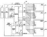
- FIG. 1 shows an example of control block diagram of a PCI control system according to a first embodiment of the present invention
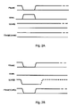
- FIG. 2A shows an example of a timing chart of each signal when the PCI host control unit shown in FIG. 1 accesses a PCI device;
- FIG. 2B shows an example of a timing chart of each signal when the PCI host control unit shown in FIG. 1 accesses a CardBus device;
- FIG. 3 shows an example of control block diagram of a PCI control system according to a second embodiment of the present invention
- FIG. 4 shows a control block diagram of a general PCI control system connecting a plurality of PCI devices to a PCI bus; and.
- FIG. 5 shows a control block diagram of a general PCI control system connecting CardBus compliant device to a PCI bus via a bridge.
- FIG. 1 shows an example of a control block diagram of a PCI control system 10 according to a first exemplary embodiment of the present invention.
- the PCI control system 10 includes a PCI host control unit 12 , PCI devices 16 A and 16 B, a CardBus device 18 and a host CPU 20 .
- the PCI host control unit 12 connects to the PCI devices 16 A and 16 B and the CardBus device 18 via a PCI bus 14 .
- the PCI host control unit 12 accesses the PCI devices 16 A and 16 B and the CardBus device 18 by directions of the host CPU 20 .
- the PCI host control unit 12 is a kind of an access control device.
- the PCI host control unit 12 includes a host bridge 101 , a CONFIG_ADDRESS register 102 , a CONFIG_DATA register 103 , a PCI cycle generator 104 and a FRAME signal generator 105 for a CardBus device.
- the Host bridge 101 is connected to the host CPU 20 , the CONFIG_ADDRESS register 102 and the CONFIG_DATA register 103 .
- the CONFIG_ADDRESS register 102 and the CONFIG_DATA register 103 are connected to the PCI cycle generator 104 .
- the PCI cycle generator 104 generates various PCI cycles (transaction) on the PCI bus 14 based on contents stored in these registers.
- AD means an address and a data signal.
- CBE means a command byte enable signal.
- IRDY means a signal indicating a completion of a data transfer preparation of an initiator.
- TRDY means a signal indicating a completion of a target preparation.
- DEVSEL means a signal indicating during transaction operation from a selected target.
- FRAME means a signal indicating transaction starting. For example, FRAME becomes active at a low level.
- IDSEL means a signal indicating a configuration cycle. For example, IDSEL becomes active at a high level.
- a configuration register includes an address space with 256 bytes. Accordingly, access to the configuration register is performed by controlling eight bit addresses. For example, when data of 0x11223344 is written in a configuration register of address 0x00, the host CPU 20 writes 0x00000000 in the CONFIG_ADDRESS register 102 and next, writes 0x11223344 in the CONFIG_DATA register 103 . Thereby, a write transaction in the address 0x00 occurs.
- the FRAME signal generator 105 When the PCI host control unit 12 accesses the CardBus device 18 , the FRAME signal generator 105 generates a FRAME (CARD) signal for the CardBus device 18 .
- the FRAME signal generator 105 includes an address judgment unit 106 and an OR gate 107 .
- the address judgment unit 106 judges whether an address written in the CONFIG_ADDRESS register 102 is an address for accessing the CardBus device 18 or an address for the accessing the PCI devices 16 A and 16 B. Specifically, the address judgment unit 106 judges whether an address written in the CONFIG_ADDRESS register 102 accords with an address of the CardBus device 18 .
- An address judgment unit 106 outputs a judgment result signal SCARD at a low level when the both addresses are identical and outputs the judgment result signal SCARD at a high level when the addresses are not identical.
- the judgment result signal SCARD of the address judgment unit 106 and the FRAME signal from the PCI cycle generator 104 enter the OR gate 107 .
- the OR gate 107 conducts logical OR operation regarding the input signals.
- the OR gate 107 outputs the logical addition result to the CardBus device 18 as a FRAME (CARD) signal.
- FIG. 2A shows an example of timing charts of signals which occur when the PCI host control unit 12 accesses a predetermined PCI device, for example, a PCI device 16 A during configuration processing.
- the PCI cycle generator 104 starts a transaction on the PCI. Specifically, the PCI cycle generator 104 outputs the FRAME signal of a low level (i.e. active signal). IDSEL of the PCI device 16 A which is an access target is set to a high level (i.e. active) as shown in FIG. 2A , and IDSEL of a PCI device which is not an access target is set to a low level (i.e.
- the address judgment unit 106 judges whether or not an address stored in the CONFIG_ADDRESS register 102 accords with an address of the CardBus device 18 .
- the address judgment unit 106 outputs the judgment result signal SCARD with a high level. Therefore, the OR gate 107 outputs the FRAME (CARD) signal with a high level regardless of a level of the FRAME signal from the PCI cycle generator 104 .
- the FRAME signal and the FRAME (CARD) signal become active when the signals are at a low level. That is, when an access target is one of the PCI device 16 A and the PCI device 16 B, the FRAME (CARD) signal becomes inactive, and the CardBus device 18 does not reply to an access. Therefore, even if the CardBus device 18 is connected to the PCI bus 14 , either of the PCI device 16 A and the PCI device 16 B is accessed certainly.
- FIG. 2B shows an example of timing charts of signals which occur when the PCI host control unit 12 accesses the CardBus device 18 during configuration processing.
- the PCI cycle generator 104 starts a transaction on the PCI. Specifically, the PCI cycle generator 104 outputs the FRAME signal with a low level (i.e. active signal).
- the address judgment unit 106 judges whether or not an address stored in the CONFIG_ADDRESS register 102 accords with an address of the CardBus device 18 .
- the address judgment unit 106 When the both addresses are in accord with each other, that is, when the CardBus device 18 is accessed, the address judgment unit 106 outputs a judgment result signal SCARD with a low level. Therefore, the OR gate 107 outputs the FRAME signal from the PCI cycle generator 104 to the CardBus device 18 as the FRAME (CARD) signal. That is, the FRAME (CARD) signal with a low level (i.e. active signal) enters the CardBus device 18 . On the other hand, the FRAME signal with a low level also enters the PCI device 16 A and the PCI device 16 B.
- the level of the IDSEL signal becomes low (i.e. inactive) as shown in FIG. 2B . Therefore, the PCI devices 16 A and 16 B do not respond to the access thereto. That is, even if one or more PCI devices (i.e. PCI device 16 A or PCI device 16 B) connect to the PCI bus 14 , the CardBus device 18 is accessed certainly.
- the FRAME (CARD) signal to the CardBus device is generated based on the FRAME signal for the PCI devices 16 A and 16 B.
- the CardBus device 18 can recognize starting of a transaction thereto in the configuration processing according to the FRAME (CARD) signal, even if the CardBus device 18 does not include IDSEL. That is, in the PCI control system 10 , the PCI devices 16 A and 16 B and the CardBus device 18 can coexist on the identical PCI bus 14 without using PCI-CardBus bridge. Since PCI-CardBus bridge becomes unnecessary, device configuration becomes simple and low-cost. Since the FRAME (CARD) signal is generated automatically without an operation of the host CPU 20 , a controlling load of devices can be decreased.
- the FRAME signal generator 105 can be an external device of the PCI host control unit 12 .
- a function of the PCI host control unit 10 can be obtained by executing a program on a program control processor.
- the program can include the address judgment unit 106 and the OR gate 107 as one program part thereof.
- the FRAME signal generator 105 is not necessarily limited to a circuit including the address judgment unit 106 and the OR gate 107 as mentioned above.
- the FRAME signal generator 105 can be made of other circuit configuration which includes an identical function. For example, when a FRAME signal is active at high level, the OR gate 107 may be changed to an AND gate.
- FIG. 3 shows an example of control block diagram of a PCI control system 200 according to a second exemplary embodiment of the present invention.
- the PCI control system 200 includes a plurality of CardBus devices (i.e. 202 A and 202 B in FIG. 3 ) which are connected to the PCI bus 14 .
- a FRAME signal generator 204 of the PCI control system 200 includes an address judgment unit 206 and OR gates 208 A and 208 B.
- the address judgment unit 206 generates judging result signals SCARD# 1 and SCARD# 2 for CardBus devices 202 A and 202 B respectively. Each judging result signal SCARD# 1 and SCARD# 2 are inputted to the OR gates 208 A and 208 B respectively.
- a FRAME signal from the PCI cycle generator 104 also enters the OR gates 208 A and 208 B in common.
- Each of the OR gates 208 A and 208 B perform logical OR operations for the FRAME signal and each judging result signal SCARD# 1 and SCARD# 2 .
- the OR gates 208 A and 208 B output FRAME (CARD) signals, which are results of the logical OR operations, to the CardBus devices 202 A and 202 B respectively.
- the PCI bus 14 can include a plurality of CardBus devices 202 A and 202 B.
- the number of the PCI device and the CardBus device connected to the PCI bus 14 may be set to three or more respectively.
- the bus control unit when a CardBus compliant device connects to a bus, the bus control unit generates a transaction start signal to the CardBus compliant device using a transaction start signal which indicates starting of transaction for accessing a device. More specifically, the bus control unit judges whether or not an address for accessing a device is an address for accessing a CardBus compliant device. When an address for accessing a device is an address for the accessing CardBus compliant device, the bus control unit outputs a transaction start signal to the CardBus compliant device as a transaction start signal only for the CardBus compliant device.
- the transaction start signal is a FRAME signal on the PCI supplied to a device other than the CardBus compliant device in common, and each of devices other than the CardBus compliant device is identified by an IDSEL signal.
- An address for accessing a device is stored in the CONFIG_ADDRESS register.
- the bus control unit When an device other than the CardBus compliant device is accessed, the bus control unit generates a transaction start signal indicating starting of transaction thereto. On the other hand, when a CardBus compliant device is accessed, the bus control unit generates a transaction start signal to the CardBus compliant device using the transaction start signal above mentioned.
- the bus control unit includes a means to generate a FRAME signal for a PC card from a FRAME signal of a PCI. For example, when it is judged that an access destination is the PC card by monitoring the CONFIG_ADDRESS register, the bus control unit outputs the FRAME signal, which is a FRAME signal for PC cards, to the PC card.
- a transaction start signal to CardBus compliant devices is generated using a transaction start signal.
- the host CPU can access an individual CardBus compliant device. Therefore, control of the host CPU becomes unnecessary, and load is reduced. Since PCI-CardBus bridge becomes unnecessary when a PC card is connected, it is possible to reduce cost, and reduce the restrictions of part arrangement at a time of hardware design.
Landscapes
- Engineering & Computer Science (AREA)
- Theoretical Computer Science (AREA)
- General Engineering & Computer Science (AREA)
- Physics & Mathematics (AREA)
- General Physics & Mathematics (AREA)
- Computer Hardware Design (AREA)
- Bus Control (AREA)
Abstract
Description
- This application is based on Japanese Patent Application No. JP 2006-287077 filed on Oct. 23, 2006, and including a specification, claims, drawings and summary. The disclosure of the above Japanese Patent Application is incorporated herein by reference in its entirety.
- 1. Field of the Invention
- The present invention relates to an access control device and an access control method.
- 2. Description of the Related Art
- As an external expansion bus of a personal computer (hereinafter, referred to a PC), or, as an internal bus in various electronic equipment, a PCI (Peripheral Component Interconnect) bus is known. The PCI bus can connect to a plurality of PCI devices. For example, as shown in
FIG. 4 , a PCIhost control unit 1 and a plurality ofPCI devices 2A-2C connect to a PCI bus 3. - On the other hand, as a standard of a bus used for a PC card, a CardBus is known. The CardBus is configured based on a PCI. However, signal specifications of the PCI bus and the CardBus are not perfectly identical. Therefore, a device 4 based upon the CardBus standard (hereinafter, referred to as a CardBus device) such as the PC card cannot be connected to the PCI bus directly. Accordingly, for example, as shown in
FIG. 5 , if the CardBus device 4 and the PCIhost control unit 1 are connected, a PCI-CardBus bridge 5 has to be interposed therebetween. The PCI-CardBusbridge 5 is large-sized and costly. Only one CardBus device can be connected to one PCI-CardBus bridge 5. - Here, reason why CardBus cannot include a plurality of CardBus will be described below. The PCI
host control unit 1 accesses thePCI devices 2A-2C via the PCI bus 3. When thePCI devices 2A-2C are recognized, the PCIhost control unit 1 performs configuration processing. A PCI includes an address space of 4 G bytes. When the configuration processing is performed, an access region of eachPCI devices 2A-2B is assigned to one of areas in the address space with 4 G bytes. For example, the access region of thePCI device 2A is assigned to 0x10000000-0x1000FFFF (0x: a hexadecimal number), and the access region of thePCI device 2B is assigned to 0x10010000-0x10010FFF, and the access region of thePCI device 2C is assigned to 0x20000000-0x20007FFF. - Information concerning the access region of each
PCI devices 2A-2C is stored in a configuration register. In the configuration processing, the PCIhost control unit 1 reads a value of the configuration register of eachPCI devices 2A-2C. By performing the configuration processing,PCI devices 2A-2C can distinguish whether predetermined access is an access addressed to itself as an address on the PCI. Accordingly, even when a plurality ofPCI devices 2A-2C are connected to a PCI bus 3, signals of the devices does not conflict. - After the configuration processing is completed, the individual address space is assigned to each
PCI devices 2A-2C. On the other hand, each configuration register itself of eachPCI devices 2A-2C is mapped in an identical address space. Therefore, accesses toPCI devices 2A-2C may conflict in the configuration processing. Thus a PCI includes an IDSEL signal which is effective only during the configuration processing. The IDSEL signal is a signal showing a configuration register of a device to be accessed. The IDSEL signal avoids an access conflict between thePCI devices 2A-2C during the configuration processing. - However, in the CardBus standard, the IDSEL signal mentioned above is not defined. Therefore, when a CardBus device 4 shown in
FIG. 5 is connected to a PCI bus 3 shown inFIG. 4 , an access conflict occurs between the CardBus device 4 and thePCI devices 2A-2C in the configuration processing. - Japanese Patent Application Laid-Open No. 2003-316725 discloses a configuration for using a device conforming to the PC card standard as a PCI device without using a bridge. In such configuration, a CPU and a bus change circuit controlled by the CPU are provided. When a PC card compliant device is accessed, a C/BE order bus is connected to the PC card compliant devices. On the other hand, when other device is accessed, the C/BE order bus is shut off from the PC card compliant device. However, in the aforementioned constitution, whenever the device is accessed, the CPU has to control the bus change circuit.
- An exemplary object of the present invention is to provide an access control device and an access control method which can simplify a device configuration without increasing a control load.
- In an exemplary aspect of the invention, an access control device controls access to a first device and a second device. The first device is connected with a first bus conforming to a first standard and conforms to the first standard. The second device is connected with the first bus and conforms to a second standard. The access control device includes a first signal generator and a second signal generator. The first signal generator generates a first transaction start signal indicating start of a transaction for the first device. The second signal generator generates a second transaction start signal for the second device based on the first transaction start signal.
- Other exemplary features and advantages of the present invention will be apparent from the following description taken in conjunction with the accompanying drawings, in which like reference characters designate the same or similar parts throughout the figures thereof.
- Exemplary features and advantages of the present invention will become apparent from the following detailed description when taken with the accompanying drawings in which:
-
FIG. 1 shows an example of control block diagram of a PCI control system according to a first embodiment of the present invention; -
FIG. 2A shows an example of a timing chart of each signal when the PCI host control unit shown inFIG. 1 accesses a PCI device; -
FIG. 2B shows an example of a timing chart of each signal when the PCI host control unit shown inFIG. 1 accesses a CardBus device; -
FIG. 3 shows an example of control block diagram of a PCI control system according to a second embodiment of the present invention; -
FIG. 4 shows a control block diagram of a general PCI control system connecting a plurality of PCI devices to a PCI bus; and. -
FIG. 5 shows a control block diagram of a general PCI control system connecting CardBus compliant device to a PCI bus via a bridge. - Hereinafter, exemplary embodiments of the present invention will be described in detail with reference to drawings.
FIG. 1 shows an example of a control block diagram of aPCI control system 10 according to a first exemplary embodiment of the present invention. ThePCI control system 10 includes a PCIhost control unit 12,PCI devices CardBus device 18 and ahost CPU 20. The PCIhost control unit 12 connects to thePCI devices CardBus device 18 via aPCI bus 14. The PCIhost control unit 12 accesses thePCI devices CardBus device 18 by directions of thehost CPU 20. The PCIhost control unit 12 is a kind of an access control device. - The PCI
host control unit 12 includes ahost bridge 101, aCONFIG_ADDRESS register 102, aCONFIG_DATA register 103, aPCI cycle generator 104 and aFRAME signal generator 105 for a CardBus device. TheHost bridge 101 is connected to thehost CPU 20, theCONFIG_ADDRESS register 102 and theCONFIG_DATA register 103. TheCONFIG_ADDRESS register 102 and theCONFIG_DATA register 103 are connected to thePCI cycle generator 104. ThePCI cycle generator 104 generates various PCI cycles (transaction) on thePCI bus 14 based on contents stored in these registers. - A signal on the
PCI bus 14 will be described. AD means an address and a data signal. CBE means a command byte enable signal. IRDY means a signal indicating a completion of a data transfer preparation of an initiator. TRDY means a signal indicating a completion of a target preparation. DEVSEL means a signal indicating during transaction operation from a selected target. FRAME means a signal indicating transaction starting. For example, FRAME becomes active at a low level. IDSEL means a signal indicating a configuration cycle. For example, IDSEL becomes active at a high level. - A configuration register includes an address space with 256 bytes. Accordingly, access to the configuration register is performed by controlling eight bit addresses. For example, when data of 0x11223344 is written in a configuration register of address 0x00, the
host CPU 20 writes 0x00000000 in theCONFIG_ADDRESS register 102 and next, writes 0x11223344 in theCONFIG_DATA register 103. Thereby, a write transaction in the address 0x00 occurs. - On the other hand, when data is read from the configuration register with address 0x10, the
host CPU 20 writes 0x10000000 in theCONFIG_ADDRESS register 102. Thereby a read transaction in the address 0x10 occurs. - When the PCI
host control unit 12 accesses theCardBus device 18, theFRAME signal generator 105 generates a FRAME (CARD) signal for theCardBus device 18. TheFRAME signal generator 105 includes anaddress judgment unit 106 and anOR gate 107. Theaddress judgment unit 106 judges whether an address written in theCONFIG_ADDRESS register 102 is an address for accessing theCardBus device 18 or an address for the accessing thePCI devices address judgment unit 106 judges whether an address written in the CONFIG_ADDRESS register 102 accords with an address of theCardBus device 18. Anaddress judgment unit 106 outputs a judgment result signal SCARD at a low level when the both addresses are identical and outputs the judgment result signal SCARD at a high level when the addresses are not identical. The judgment result signal SCARD of theaddress judgment unit 106 and the FRAME signal from thePCI cycle generator 104 enter theOR gate 107. The ORgate 107 conducts logical OR operation regarding the input signals. The ORgate 107 outputs the logical addition result to theCardBus device 18 as a FRAME (CARD) signal. -
FIG. 2A shows an example of timing charts of signals which occur when the PCIhost control unit 12 accesses a predetermined PCI device, for example, aPCI device 16A during configuration processing. When thehost CPU 20 accesses theCONFIG_ADDRESS register 102 and theCONFIG_DATA register 103, thePCI cycle generator 104 starts a transaction on the PCI. Specifically, thePCI cycle generator 104 outputs the FRAME signal of a low level (i.e. active signal). IDSEL of thePCI device 16A which is an access target is set to a high level (i.e. active) as shown inFIG. 2A , and IDSEL of a PCI device which is not an access target is set to a low level (i.e. inactive, not shown). Since theCardBus device 18 is not equipped with IDSEL, theCardBus device 18 is not affected by ISDEL at all. Theaddress judgment unit 106 judges whether or not an address stored in the CONFIG_ADDRESS register 102 accords with an address of theCardBus device 18. When the both addresses are not in accord with each other, that is, when any one ofPCI device 16A andPCI device 16B are accessed, theaddress judgment unit 106 outputs the judgment result signal SCARD with a high level. Therefore, theOR gate 107 outputs the FRAME (CARD) signal with a high level regardless of a level of the FRAME signal from thePCI cycle generator 104. The FRAME signal and the FRAME (CARD) signal become active when the signals are at a low level. That is, when an access target is one of thePCI device 16A and thePCI device 16B, the FRAME (CARD) signal becomes inactive, and theCardBus device 18 does not reply to an access. Therefore, even if theCardBus device 18 is connected to thePCI bus 14, either of thePCI device 16A and thePCI device 16B is accessed certainly. -
FIG. 2B shows an example of timing charts of signals which occur when the PCIhost control unit 12 accesses theCardBus device 18 during configuration processing. When thehost CPU 20 accesses theCONFIG_ADDRESS register 102 and theCONFIG_DATA register 103, thePCI cycle generator 104 starts a transaction on the PCI. Specifically, thePCI cycle generator 104 outputs the FRAME signal with a low level (i.e. active signal). Theaddress judgment unit 106 judges whether or not an address stored in the CONFIG_ADDRESS register 102 accords with an address of theCardBus device 18. When the both addresses are in accord with each other, that is, when theCardBus device 18 is accessed, theaddress judgment unit 106 outputs a judgment result signal SCARD with a low level. Therefore, theOR gate 107 outputs the FRAME signal from thePCI cycle generator 104 to theCardBus device 18 as the FRAME (CARD) signal. That is, the FRAME (CARD) signal with a low level (i.e. active signal) enters theCardBus device 18. On the other hand, the FRAME signal with a low level also enters thePCI device 16A and thePCI device 16B. However, because both of thePCI device 16A and thePCI device 16B are not targets to be accessed, the level of the IDSEL signal becomes low (i.e. inactive) as shown inFIG. 2B . Therefore, thePCI devices PCI device 16A orPCI device 16B) connect to thePCI bus 14, theCardBus device 18 is accessed certainly. - As described above, in the
PCI control system 10 of the first exemplary embodiment of the present invention, the FRAME (CARD) signal to the CardBus device is generated based on the FRAME signal for thePCI devices CardBus device 18 can recognize starting of a transaction thereto in the configuration processing according to the FRAME (CARD) signal, even if theCardBus device 18 does not include IDSEL. That is, in thePCI control system 10, thePCI devices CardBus device 18 can coexist on theidentical PCI bus 14 without using PCI-CardBus bridge. Since PCI-CardBus bridge becomes unnecessary, device configuration becomes simple and low-cost. Since the FRAME (CARD) signal is generated automatically without an operation of thehost CPU 20, a controlling load of devices can be decreased. - An example of the
FRAME signal generator 105 provided in the PCIhost control unit 12 is described above. TheFRAME signal generator 105, however, can be an external device of the PCIhost control unit 12. - A function of the PCI
host control unit 10 can be obtained by executing a program on a program control processor. The program can include theaddress judgment unit 106 and theOR gate 107 as one program part thereof. - The
FRAME signal generator 105 is not necessarily limited to a circuit including theaddress judgment unit 106 and theOR gate 107 as mentioned above. TheFRAME signal generator 105 can be made of other circuit configuration which includes an identical function. For example, when a FRAME signal is active at high level, theOR gate 107 may be changed to an AND gate. -
FIG. 3 shows an example of control block diagram of aPCI control system 200 according to a second exemplary embodiment of the present invention. ThePCI control system 200 includes a plurality of CardBus devices (i.e. 202A and 202B inFIG. 3 ) which are connected to thePCI bus 14. AFRAME signal generator 204 of thePCI control system 200 includes anaddress judgment unit 206 and ORgates 208A and 208B. Theaddress judgment unit 206 generates judging result signalsSCARD# 1 andSCARD# 2 forCardBus devices signal SCARD# 1 andSCARD# 2 are inputted to theOR gates 208A and 208B respectively. A FRAME signal from thePCI cycle generator 104 also enters the ORgates 208A and 208B in common. Each of theOR gates 208A and 208B perform logical OR operations for the FRAME signal and each judging resultsignal SCARD# 1 andSCARD# 2. The ORgates 208A and 208B output FRAME (CARD) signals, which are results of the logical OR operations, to theCardBus devices PCI bus 14 can include a plurality ofCardBus devices - The number of the PCI device and the CardBus device connected to the
PCI bus 14 may be set to three or more respectively. - According to the third exemplary embodiment of the present invention, when a CardBus compliant device connects to a bus, the bus control unit generates a transaction start signal to the CardBus compliant device using a transaction start signal which indicates starting of transaction for accessing a device. More specifically, the bus control unit judges whether or not an address for accessing a device is an address for accessing a CardBus compliant device. When an address for accessing a device is an address for the accessing CardBus compliant device, the bus control unit outputs a transaction start signal to the CardBus compliant device as a transaction start signal only for the CardBus compliant device.
- For example, the transaction start signal is a FRAME signal on the PCI supplied to a device other than the CardBus compliant device in common, and each of devices other than the CardBus compliant device is identified by an IDSEL signal. An address for accessing a device is stored in the CONFIG_ADDRESS register.
- When an device other than the CardBus compliant device is accessed, the bus control unit generates a transaction start signal indicating starting of transaction thereto. On the other hand, when a CardBus compliant device is accessed, the bus control unit generates a transaction start signal to the CardBus compliant device using the transaction start signal above mentioned.
- Only when accessing to a PC card, the bus control unit includes a means to generate a FRAME signal for a PC card from a FRAME signal of a PCI. For example, when it is judged that an access destination is the PC card by monitoring the CONFIG_ADDRESS register, the bus control unit outputs the FRAME signal, which is a FRAME signal for PC cards, to the PC card.
- In the above-mentioned embodiment, a transaction start signal to CardBus compliant devices is generated using a transaction start signal. By the signal, the host CPU can access an individual CardBus compliant device. Therefore, control of the host CPU becomes unnecessary, and load is reduced. Since PCI-CardBus bridge becomes unnecessary when a PC card is connected, it is possible to reduce cost, and reduce the restrictions of part arrangement at a time of hardware design.
- The previous description of embodiments is provided to enable a person skilled in the art to make and use the present invention. Moreover, various modifications to these embodiments will be readily apparent to those skilled in the art, and the generic principles and specific examples defined herein may be applied to other embodiments without the use of inventive faculty. Therefore, the present invention is not intended to be limited to the embodiments described herein but is to be accorded the widest scope as defined by the limitations of the claims and equivalents.
- Further, it is noted that the inventor's intent is to retain all equivalents of the claimed invention even if the claims are amended during prosecution.
- While this invention has been described in connection with certain preferred embodiments, it is to be understood that the subject matter encompassed by way of this invention is not to be limited to those specific embodiments. On the contrary, it is intended for the subject matter of the invention to include all alternative, modification and equivalents as can be included within the spirit and scope of the following claims.
- Further, it is the inventor's intention to retain all equivalents of the claimed invention even if the claims are amended during prosecution.
Claims (18)
Applications Claiming Priority (3)
| Application Number | Priority Date | Filing Date | Title |
|---|---|---|---|
| JP287077/2006 | 2006-10-23 | ||
| JP2006287077A JP4257358B2 (en) | 2006-10-23 | 2006-10-23 | Bus control method and apparatus |
| JP2006-287077 | 2006-10-23 |
Publications (2)
| Publication Number | Publication Date |
|---|---|
| US20080098140A1 true US20080098140A1 (en) | 2008-04-24 |
| US7698494B2 US7698494B2 (en) | 2010-04-13 |
Family
ID=39319394
Family Applications (1)
| Application Number | Title | Priority Date | Filing Date |
|---|---|---|---|
| US11/876,044 Active 2028-04-23 US7698494B2 (en) | 2006-10-23 | 2007-10-22 | Access control device and access control method |
Country Status (5)
| Country | Link |
|---|---|
| US (1) | US7698494B2 (en) |
| JP (1) | JP4257358B2 (en) |
| KR (1) | KR100975950B1 (en) |
| CN (1) | CN101169767B (en) |
| TW (1) | TWI354897B (en) |
Families Citing this family (3)
| Publication number | Priority date | Publication date | Assignee | Title |
|---|---|---|---|---|
| JP2009294821A (en) | 2008-06-04 | 2009-12-17 | Sony Corp | Information processor, information processing method, program, and information processing system |
| KR101645388B1 (en) | 2010-03-15 | 2016-08-03 | 니켄 코가쿠 가부시키가이샤 | Wave-dissipating block formwork apparatus |
| JP5429130B2 (en) * | 2010-10-13 | 2014-02-26 | ソニー株式会社 | Information processing apparatus and information processing method |
Citations (2)
| Publication number | Priority date | Publication date | Assignee | Title |
|---|---|---|---|---|
| US5931932A (en) * | 1997-05-12 | 1999-08-03 | Cirrus Logic, Inc. | Dynamic retry mechanism to prevent corrupted data based on posted transactions on the PCI bus |
| US20030110335A1 (en) * | 2000-06-12 | 2003-06-12 | Ncr Corporation | Bus transaction between devices in a system |
Family Cites Families (4)
| Publication number | Priority date | Publication date | Assignee | Title |
|---|---|---|---|---|
| JP3895071B2 (en) | 1999-03-12 | 2007-03-22 | インターナショナル・ビジネス・マシーンズ・コーポレーション | Bus / bridge circuit, information processing system, and card bus controller |
| JP2000322376A (en) | 1999-05-10 | 2000-11-24 | Nec Corp | Bus interface converting circuit |
| JP2003316725A (en) | 2002-04-19 | 2003-11-07 | Youxun Sci & Technol Co Ltd | Circuit and method for using elements permitted by the PC card bus standard in an electronic device to which the PCI bus standard is applied |
| US7028130B2 (en) * | 2003-08-14 | 2006-04-11 | Texas Instruments Incorporated | Generating multiple traffic classes on a PCI Express fabric from PCI devices |
-
2006
- 2006-10-23 JP JP2006287077A patent/JP4257358B2/en not_active Expired - Fee Related
-
2007
- 2007-10-17 KR KR1020070104648A patent/KR100975950B1/en not_active Expired - Fee Related
- 2007-10-22 US US11/876,044 patent/US7698494B2/en active Active
- 2007-10-22 TW TW096139437A patent/TWI354897B/en not_active IP Right Cessation
- 2007-10-23 CN CN200710180294.0A patent/CN101169767B/en not_active Expired - Fee Related
Patent Citations (2)
| Publication number | Priority date | Publication date | Assignee | Title |
|---|---|---|---|---|
| US5931932A (en) * | 1997-05-12 | 1999-08-03 | Cirrus Logic, Inc. | Dynamic retry mechanism to prevent corrupted data based on posted transactions on the PCI bus |
| US20030110335A1 (en) * | 2000-06-12 | 2003-06-12 | Ncr Corporation | Bus transaction between devices in a system |
Also Published As
| Publication number | Publication date |
|---|---|
| TWI354897B (en) | 2011-12-21 |
| JP4257358B2 (en) | 2009-04-22 |
| US7698494B2 (en) | 2010-04-13 |
| TW200836071A (en) | 2008-09-01 |
| CN101169767A (en) | 2008-04-30 |
| KR100975950B1 (en) | 2010-08-13 |
| JP2008102886A (en) | 2008-05-01 |
| KR20080036522A (en) | 2008-04-28 |
| CN101169767B (en) | 2014-01-29 |
Similar Documents
| Publication | Publication Date | Title |
|---|---|---|
| US5649128A (en) | Multiple bus interface adapter for connection to a plurality of computer bus architectures | |
| US5761462A (en) | Method and system for supporting peripheral component interconnect (PCI) peer-to-peer access across multiple PCI host bridges within a data-processing system | |
| KR100306636B1 (en) | PCI-ISA Interrupt Protocol Converter and Selection Mechanism | |
| US6598177B1 (en) | Monitoring error conditions in an integrated circuit | |
| US5655142A (en) | High performance derived local bus and computer system employing the same | |
| JP2002351822A (en) | Set up of selective destination of transactions to devices on a shared bus | |
| AU721685B2 (en) | Bus interface control circuit | |
| WO2001006363A1 (en) | A method for improving interrupt response time | |
| JP2002539524A (en) | Apparatus and method for handling peripheral device interrupts | |
| JP2003296267A (en) | Bus system and information processing system including bus system | |
| US11409679B2 (en) | System component and use of a system component | |
| KR100241514B1 (en) | Micro computer | |
| US6145044A (en) | PCI bus bridge with transaction forwarding controller for avoiding data transfer errors | |
| US7698494B2 (en) | Access control device and access control method | |
| US5933613A (en) | Computer system and inter-bus control circuit | |
| US6883057B2 (en) | Method and apparatus embedding PCI-to-PCI bridge functions in PCI devices using PCI configuration header type 0 | |
| US6550015B1 (en) | Scalable virtual timer architecture for efficiently implementing multiple hardware timers with minimal silicon overhead | |
| US5761461A (en) | Method and system for preventing peripheral component interconnect (PCI) peer-to-peer access across multiple PCI host bridges within a data processing system | |
| US7636797B2 (en) | LPC configuration sharing method | |
| JP3859173B2 (en) | General-purpose operator station module for distributed process control systems. | |
| JP5146796B2 (en) | Host controller | |
| JP3525771B2 (en) | Bus snoop control circuit | |
| JP5431823B2 (en) | Semiconductor device | |
| JP2001027920A (en) | Bus bridge circuit and its power management method | |
| JP2008305232A (en) | PC card device |
Legal Events
| Date | Code | Title | Description |
|---|---|---|---|
| AS | Assignment |
Owner name: NEC ACCESS TECHNICA, LTD., JAPAN Free format text: ASSIGNMENT OF ASSIGNORS INTEREST;ASSIGNOR:KATO, TETSUYA;REEL/FRAME:019992/0374 Effective date: 20071011 Owner name: NEC ACCESS TECHNICA, LTD.,JAPAN Free format text: ASSIGNMENT OF ASSIGNORS INTEREST;ASSIGNOR:KATO, TETSUYA;REEL/FRAME:019992/0374 Effective date: 20071011 |
|
| STCF | Information on status: patent grant |
Free format text: PATENTED CASE |
|
| FPAY | Fee payment |
Year of fee payment: 4 |
|
| AS | Assignment |
Owner name: NEC PLATFORMS, LTD., JAPAN Free format text: MERGER AND CHANGE OF NAME;ASSIGNORS:NEC ACCESSTECHNICA, LTD.;NEC INFRONTIA CORPORATION;REEL/FRAME:034906/0402 Effective date: 20140701 |
|
| MAFP | Maintenance fee payment |
Free format text: PAYMENT OF MAINTENANCE FEE, 8TH YEAR, LARGE ENTITY (ORIGINAL EVENT CODE: M1552) Year of fee payment: 8 |
|
| MAFP | Maintenance fee payment |
Free format text: PAYMENT OF MAINTENANCE FEE, 12TH YEAR, LARGE ENTITY (ORIGINAL EVENT CODE: M1553); ENTITY STATUS OF PATENT OWNER: LARGE ENTITY Year of fee payment: 12 |