US20060278564A1 - Thin-plate supporting container - Google Patents
Thin-plate supporting container Download PDFInfo
- Publication number
- US20060278564A1 US20060278564A1 US11/444,501 US44450106A US2006278564A1 US 20060278564 A1 US20060278564 A1 US 20060278564A1 US 44450106 A US44450106 A US 44450106A US 2006278564 A1 US2006278564 A1 US 2006278564A1
- Authority
- US
- United States
- Prior art keywords
- thin
- plate supporting
- inclined plane
- engagement protrusion
- container body
- Prior art date
- Legal status (The legal status is an assumption and is not a legal conclusion. Google has not performed a legal analysis and makes no representation as to the accuracy of the status listed.)
- Abandoned
Links
Images


Classifications
-
- H—ELECTRICITY
- H10—SEMICONDUCTOR DEVICES; ELECTRIC SOLID-STATE DEVICES NOT OTHERWISE PROVIDED FOR
- H10P—GENERIC PROCESSES OR APPARATUS FOR THE MANUFACTURE OR TREATMENT OF DEVICES COVERED BY CLASS H10
- H10P95/00—Generic processes or apparatus for manufacture or treatments not covered by the other groups of this subclass
-
- H—ELECTRICITY
- H10—SEMICONDUCTOR DEVICES; ELECTRIC SOLID-STATE DEVICES NOT OTHERWISE PROVIDED FOR
- H10P—GENERIC PROCESSES OR APPARATUS FOR THE MANUFACTURE OR TREATMENT OF DEVICES COVERED BY CLASS H10
- H10P72/00—Handling or holding of wafers, substrates or devices during manufacture or treatment thereof
- H10P72/10—Handling or holding of wafers, substrates or devices during manufacture or treatment thereof using carriers specially adapted therefor, e.g. front opening unified pods [FOUP]
- H10P72/19—Handling or holding of wafers, substrates or devices during manufacture or treatment thereof using carriers specially adapted therefor, e.g. front opening unified pods [FOUP] closed carriers
- H10P72/1918—Handling or holding of wafers, substrates or devices during manufacture or treatment thereof using carriers specially adapted therefor, e.g. front opening unified pods [FOUP] closed carriers characterised by coupling elements, kinematic members, handles or elements to be externally gripped
-
- B—PERFORMING OPERATIONS; TRANSPORTING
- B65—CONVEYING; PACKING; STORING; HANDLING THIN OR FILAMENTARY MATERIAL
- B65D—CONTAINERS FOR STORAGE OR TRANSPORT OF ARTICLES OR MATERIALS, e.g. BAGS, BARRELS, BOTTLES, BOXES, CANS, CARTONS, CRATES, DRUMS, JARS, TANKS, HOPPERS, FORWARDING CONTAINERS; ACCESSORIES, CLOSURES, OR FITTINGS THEREFOR; PACKAGING ELEMENTS; PACKAGES
- B65D85/00—Containers, packaging elements or packages, specially adapted for particular articles or materials
- B65D85/30—Containers, packaging elements or packages, specially adapted for particular articles or materials for articles particularly sensitive to damage by shock or pressure
-
- H—ELECTRICITY
- H10—SEMICONDUCTOR DEVICES; ELECTRIC SOLID-STATE DEVICES NOT OTHERWISE PROVIDED FOR
- H10P—GENERIC PROCESSES OR APPARATUS FOR THE MANUFACTURE OR TREATMENT OF DEVICES COVERED BY CLASS H10
- H10P72/00—Handling or holding of wafers, substrates or devices during manufacture or treatment thereof
- H10P72/50—Handling or holding of wafers, substrates or devices during manufacture or treatment thereof for positioning, orientation or alignment
Definitions
- the present invention relates to a thin-plate supporting container which has positioning means for positioning a placement table to a set position in order to take in and out thin plates.
- the top flange 5 is detachably mounted to the outside of the side wall 2 B which functions as a top part in the horizontal state.
- the carrying handle 6 is detachably mounted to the outside of the side walls 2 C and 2 D which function as side parts in the horizontal state.
- the positioning means 11 is provided to the side wall 2 A.
- the positioning means 11 is composed mainly of three engagement grooves 12 .
- Each of the engagement grooves 12 has a first engagement groove 12 A which aligns with the vertical direction of the container body 2 , and a second groove 12 B and a third groove 12 C both of which are inclined at the same angle (approximately 60 degrees) to the vertical direction of the container body 2 .
- These three engagement grooves 12 are finished at high precision to meet their standard.
- Each of the engagement grooves 12 A, 12 B, and 12 C has an inclined plane 13 as an inner wall, and the inner wall 13 is configured to be directly in contact with an engagement protrusion (not shown) of a placement table side.
- the inclined plane 13 is in contact with the engagement protrusion and slides, and each central position of each of the engagement grooves 12 A, 12 B, and 12 C aligns at the central position of the each engagement protrusion.
- the thin-plate supporting container 1 is set at an exact location, an arm part of the wafer transferring robot supports a semiconductor wafer and takes the semiconductor wafer in and out.
- each inclined plane 13 of each of the engagement grooves 12 A, 12 B, and 12 C is formed in a flat plane. Accordingly, a contact area between the inclined plane 13 and the engagement protrusion of the placement table side becomes large.
- the thin-plate supporting container such as polycarbonate
- some construction materials of the thin-plate supporting container such as polycarbonate
- the friction resistance becomes larger.
- the inclined plane 13 and the engagement protrusion of the placement table side become hard to slide, sometimes it is hard to readily position the thin-plate supporting container.
- the present invention has been made to solve the above drawbacks. It is an object of the present invention to provide a thin-plate supporting container capable of readily and precisely perform positioning.
- the positioning means includes an engagement groove for engaging an engagement protrusion provided on the placement table, and a inclined plane to be in contact with the engagement protrusion in a state the engagement groove engages with the engagement protrusion, and the inclined plane is treated so that friction resistance is reduced.
- the inclined plane of the engagement groove in the positioning means is subjected to embossing formed by shot peening and sandblasting and the like, so as to reduce a contact area of the inclined plane and the engagement protrusion to reduce the friction resistance.
- the inclined plane of the engagement groove in the positioning means is treated so as to reduce the friction resistance by embossing, and the like, if the engagement groove in the positioning means is fit to the engagement protrusion, the inclined plane of the engagement groove in the positioning means smoothly slide against the engagement protrusion and the precise positioning of the thin-plate supporting container is enabled.
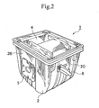
- FIG. 2 is a perspective view showing a conventional thin-plate supporting container
- FIG. 3 is a perspective view showing the conventional thin-plate supporting container in a state in which the lid is removed.
- FIG. 4 is an elevational view of the conventional thin-plate supporting container.
- the thin-plate supporting container according to embodiments of the present invention is preferably used as a container for housing, storing, and transporting a thin-plate such as a semiconductor wafer, a storage disk, a liquid crystal glass substrate, and the like.
- a thin-plate supporting container for housing a semiconductor wafer will be described.
- the overall structure of the thin-plate supporting container according to this embodiment is substantially similar to that of the above-described conventional thin-plate supporting container. Hereinafter, the description will be schematically made.
- a thin-plate supporting container 21 mainly includes a container body 22 for housing therein a plurality of semiconductor wafers (not shown), two thin-plate supporting parts (not shown) provided in the container body 22 each provided opposite to each other for supporting the semiconductor wafers, and a lid (not shown) for covering the container body 22 .
- the container body 22 is structured substantially similar in the overall shape to the container body 2 of the conventional thin-plate supporting container 1 .
- positioning means 23 of the thin-plate supporting container 21 is provided.
- the positioning means 23 is provided to the side wall 22 A.
- the positioning means 23 is composed mainly of three engagement grooves 24 .
- the engagement grooves 24 have a first engagement groove 24 A which aligns with the vertical direction of the container body 22 , and a second groove 24 B and a third groove 24 C both of which are inclined at the same angle (approximately 60 degrees) to the vertical direction of the container body 22 .
- the three engagement grooves 24 A, 24 B and 24 C are finished at high precision to meet their standard.
- Each engagement grooves 24 A, 24 B and 24 C is configured to engage with an engagement protrusion (not shown) of the placement table side, and has an inclined plane 25 as an inner wall.
- the inclined plane 25 is configured to be directly in contact with the engagement protrusion of the placement table.
- Each engagement grove 24 has an inclined plate 26 which is integrally provided on the surface of the side wall part 22 A. By placing two inclined plates 26 so as to opposite each other, each engagement groove 24 and each inclined plane 25 is structured.
- the inclined plate 26 has elasticity, and sags in some degree by being contact with the engagement protrusion of the placement table.
- the surface of the inclined plane 25 is treated in order to reduce the contact area so that the friction resistance is reduced.
- the surface of the inclined plane 25 is subject to embossing in order to reduce the friction resistance.
- fine grooves which are vertical in the ridge line direction and have a cross section of arc shape, triangular shape, or trapezoidal shape, can be regularly or irregularly formed.
- protrusions of hemispheric shape, cone shape, or truncated trapezoidal shape can be regularly or irregularly formed. Further, grooves and protrusions of each shape can be appropriately combined.
- structured thin-plate supporting container 21 is used as described below.
- the thin-plate supporting container 21 When a semiconductor wafer is automatically taken in and out to the thin-plate supporting container 21 , the thin-plate supporting container 21 is placed on the placement table. Then, the positioning means 23 of the container body 22 is fit to the engagement protrusion on the placement table. In particular, the engagement groove 24 is fit to the engagement protrusion and the inclined plane 25 is in contact with the engagement protrusion.
- the engagement protrusion is displaced against the inclined plane 25 .
- the inclined plane 25 smoothly slides against the engagement protrusion and corrects the displacement, and displaces the engagement groove 24 to the precise position.
- the inclined plate 26 is elastically sagged, preventing the friction resistance from increasing too much due to the pressure increased more than necessary at the contact portion of the inclined plane 25 and the engagement protrusion, and a smooth slide against the engagement protrusion of the inclined plane 25 is ensured.
- the slide of the inclined plane 25 against the engagement protrusion occurs at the three engagement grooves 24 A, 24 B, and 24 C respectively, and the thin-plate supporting container 21 is precisely positioned.
- an arm part of the wafer transferring robot supports the semiconductor wafer and takes in and out the semiconductor wafer to the thin-plate supporting container 21 .
- the inclined plane 25 of the engagement groove 24 in the positioning means 23 is treated so as to reduce the friction resistance by embossing, and the like, when the inclined plane 25 of the engagement groove 24 is fit to the engagement protrusion of the placement table, the inclined plane 25 and the engagement protrusion smoothly slide and the precise and easy positioning of the thin-plate supporting container is enabled.
- the inclined plane 25 is composed of the inclined plate 26 which can be elastically sagged, even if the pressure increases more than necessary at the contact portion of the inclined plane 25 and the engagement protrusion, the inclined plate 26 is elastically sagged. Accordingly, the friction resistance is prevented from increasing too much, and the smooth slide against the engagement protrusion of the inclined plane 25 is ensured. As a result, it is possible to precisely position the thin-plate supporting container.
Landscapes
- Engineering & Computer Science (AREA)
- Mechanical Engineering (AREA)
- Container, Conveyance, Adherence, Positioning, Of Wafer (AREA)
- Packaging Frangible Articles (AREA)
Abstract
When a thin-plate supporting container is placed on a placement table, a displacement is corrected and the thin-plate supporting container is precisely positioned. The thin-plate supporting container includes a container body 22 for housing therein a semiconductor wafer and the like and positioning means 23 provided to the container body 22 for positioning the container body at a set position on a placement table to place the container body on the placement table and take in and out the semiconductor wafer and the like. The positioning means 23 includes an engagement groove 24 for engaging an engagement protrusion provided on the placement table, and an inclined plane 25 to be in contact with the engagement protrusion in a state the engagement groove engages with the engagement protrusion. The inclined plane is treated so as to reduce a contact area with the engagement protrusion to decrease the friction resistance by embossing.
Description
- This application claims, under 35 USC 119, priority of Japanese Application No. 2005-172441 filed Jun. 13, 2005.
- 1. Field of the Invention
- The present invention relates to a thin-plate supporting container which has positioning means for positioning a placement table to a set position in order to take in and out thin plates.
- 2. Description of the Related Art
- A thin-plate supporting container used for automatically taking in and out an internal semiconductor wafer and the like is generally known. In such thin-plate supporting container, in order to align a position of an arm of a transfer device and a position of a semiconductor wafer and the like, positioning means is provided. As an example of the thin-plate supporting container equipped with the positioning means, a thin-plate supporting container disclosed in WO 99/39994 is known. With reference to FIGS. 2 to 4, the thin-plate supporting container will be described.
- A thin-
plate supporting container 1 shown in the drawings has acontainer body 2 which houses therein a plurality of semiconductor wafers (not shown), two thin-plate supporting parts (not shown) each provided on opposing side walls of thecontainer body 2 respectively for supporting the semiconductor wafers housed in thecontainer body 2 from the both sides of the wafers, alid 4 for covering an opening 2F of thecontainer body 2, atop flange 5 which is supported by an arm of a transfer device (not shown) if necessary, and acarrying handle 6 which is gripped by an operator when he carries the thin-plate supporting container 1 by hand. - The
container body 2 is formed substantially in the shape of a cube as a whole. The container body is, in an upright position (in the state shown in FIGS. 2 to 4), composed of fourside walls container body 2. Thecontainer body 2 is placed in a horizontal position when thecontainer body 2 is placed opposite to a wafer transferring robot (not shown) in a semiconductor wafer manufacturing line or the like. In the horizontal state, positioning means 11 which positions the thin-plate supporting container 1 is provided to the outside of theside wall 2A which functions as a bottom part. Thetop flange 5 is detachably mounted to the outside of theside wall 2B which functions as a top part in the horizontal state. Thecarrying handle 6 is detachably mounted to the outside of theside walls - The positioning means 11 is provided to the
side wall 2A. The positioning means 11 is composed mainly of threeengagement grooves 12. Each of theengagement grooves 12 has afirst engagement groove 12A which aligns with the vertical direction of thecontainer body 2, and asecond groove 12B and athird groove 12C both of which are inclined at the same angle (approximately 60 degrees) to the vertical direction of thecontainer body 2. These threeengagement grooves 12 are finished at high precision to meet their standard. Each of theengagement grooves inclined plane 13 as an inner wall, and theinner wall 13 is configured to be directly in contact with an engagement protrusion (not shown) of a placement table side. By each of theengagement grooves inclined plane 13 is in contact with the engagement protrusion and slides, and each central position of each of theengagement grooves engagement grooves plate supporting container 1 is set at an exact location, an arm part of the wafer transferring robot supports a semiconductor wafer and takes the semiconductor wafer in and out. - In the thin-plate supporting container, each
inclined plane 13 of each of theengagement grooves inclined plane 13 and the engagement protrusion of the placement table side becomes large. - Meanwhile, some construction materials of the thin-plate supporting container, such as polycarbonate, have a large friction resistance. Accordingly, as the contact area between the
inclined plane 13 and the engagement protrusion of the placement table side becomes large, the friction resistance becomes larger. As a result, theinclined plane 13 and the engagement protrusion of the placement table side become hard to slide, sometimes it is hard to readily position the thin-plate supporting container. - The present invention has been made to solve the above drawbacks. It is an object of the present invention to provide a thin-plate supporting container capable of readily and precisely perform positioning.
- It is another aspect of the present invention to provide a thin-plate supporting container having a container body for housing therein a thin-plate, and positioning means provided to the container body for positioning the container body at a set position on a placement table to place the container body on the placement table and take in and out the internal thin-plate plate. The positioning means includes an engagement groove for engaging an engagement protrusion provided on the placement table, and a inclined plane to be in contact with the engagement protrusion in a state the engagement groove engages with the engagement protrusion, and the inclined plane is treated so that friction resistance is reduced.
- Preferably, the inclined plane of the engagement groove in the positioning means is subjected to embossing formed by shot peening and sandblasting and the like, so as to reduce a contact area of the inclined plane and the engagement protrusion to reduce the friction resistance.
- Since the inclined plane of the engagement groove in the positioning means is treated so as to reduce the friction resistance by embossing, and the like, if the engagement groove in the positioning means is fit to the engagement protrusion, the inclined plane of the engagement groove in the positioning means smoothly slide against the engagement protrusion and the precise positioning of the thin-plate supporting container is enabled.
-
FIG. 1 is an elevational view of a thin-plate supporting container according to an embodiment of the present invention; -
FIG. 2 is a perspective view showing a conventional thin-plate supporting container; -
FIG. 3 is a perspective view showing the conventional thin-plate supporting container in a state in which the lid is removed; and -
FIG. 4 is an elevational view of the conventional thin-plate supporting container. - Hereinafter, a thin-plate supporting container according to embodiments of the present invention will be described with reference to the attached drawings.
- The thin-plate supporting container according to embodiments of the present invention is preferably used as a container for housing, storing, and transporting a thin-plate such as a semiconductor wafer, a storage disk, a liquid crystal glass substrate, and the like. In this embodiment, a thin-plate supporting container for housing a semiconductor wafer will be described. The overall structure of the thin-plate supporting container according to this embodiment is substantially similar to that of the above-described conventional thin-plate supporting container. Hereinafter, the description will be schematically made.
- As shown in
FIG. 1 , a thin-plate supporting container 21 according to this embodiment mainly includes acontainer body 22 for housing therein a plurality of semiconductor wafers (not shown), two thin-plate supporting parts (not shown) provided in thecontainer body 22 each provided opposite to each other for supporting the semiconductor wafers, and a lid (not shown) for covering thecontainer body 22. - The
container body 22 is structured substantially similar in the overall shape to thecontainer body 2 of the conventional thin-plate supporting container 1. To the outside of aside wall 22A which functions as a bottom part in a horizontally-placed state, positioning means 23 of the thin-plate supporting container 21 is provided. - The positioning means 23 is provided to the
side wall 22A. The positioning means 23 is composed mainly of threeengagement grooves 24. Theengagement grooves 24 have afirst engagement groove 24A which aligns with the vertical direction of thecontainer body 22, and asecond groove 24B and athird groove 24C both of which are inclined at the same angle (approximately 60 degrees) to the vertical direction of thecontainer body 22. The threeengagement grooves inclined plane 25 as an inner wall. Theinclined plane 25 is configured to be directly in contact with the engagement protrusion of the placement table. Eachengagement grove 24 has aninclined plate 26 which is integrally provided on the surface of theside wall part 22A. By placing twoinclined plates 26 so as to opposite each other, each engagement groove 24 and eachinclined plane 25 is structured. Theinclined plate 26 has elasticity, and sags in some degree by being contact with the engagement protrusion of the placement table. - The surface of the
inclined plane 25 is treated in order to reduce the contact area so that the friction resistance is reduced. In particular, the surface of theinclined plane 25 is subject to embossing in order to reduce the friction resistance. It can also be possible to drawn the surface of theinclined plane 25 to be in a concave-convex state such as a stain finished surface, or form numerous fine grooves. In the case in which the numerous fine grooves are formed, the grooves should be formed in a direction that the engagement groove displaces along theinclined plane 25. Further, on the surface of theinclined plane 25, fine grooves which are vertical in the ridge line direction and have a cross section of arc shape, triangular shape, or trapezoidal shape, can be regularly or irregularly formed. Further, protrusions of hemispheric shape, cone shape, or truncated trapezoidal shape, can be regularly or irregularly formed. Further, grooves and protrusions of each shape can be appropriately combined. - Operation
- Thus structured thin-
plate supporting container 21 is used as described below. - When a semiconductor wafer is automatically taken in and out to the thin-
plate supporting container 21, the thin-plate supporting container 21 is placed on the placement table. Then, the positioning means 23 of thecontainer body 22 is fit to the engagement protrusion on the placement table. In particular, theengagement groove 24 is fit to the engagement protrusion and theinclined plane 25 is in contact with the engagement protrusion. - Then, when the thin-
plate supporting container 21 is placed in a state displaced from a set position, the engagement protrusion is displaced against theinclined plane 25. And when the thin-plate supporting container 21 is placed on the placement table in the displaced state, due to the weight of the thin-plate supporting container 21, theinclined plane 25 smoothly slides against the engagement protrusion and corrects the displacement, and displaces theengagement groove 24 to the precise position. Then, theinclined plate 26 is elastically sagged, preventing the friction resistance from increasing too much due to the pressure increased more than necessary at the contact portion of theinclined plane 25 and the engagement protrusion, and a smooth slide against the engagement protrusion of theinclined plane 25 is ensured. Thus, the slide of theinclined plane 25 against the engagement protrusion occurs at the threeengagement grooves plate supporting container 21 is precisely positioned. - Then, an arm part of the wafer transferring robot supports the semiconductor wafer and takes in and out the semiconductor wafer to the thin-
plate supporting container 21. - Advantages
- As described above, the
inclined plane 25 of theengagement groove 24 in the positioning means 23 is treated so as to reduce the friction resistance by embossing, and the like, when theinclined plane 25 of theengagement groove 24 is fit to the engagement protrusion of the placement table, theinclined plane 25 and the engagement protrusion smoothly slide and the precise and easy positioning of the thin-plate supporting container is enabled. - Further, since the
inclined plane 25 is composed of theinclined plate 26 which can be elastically sagged, even if the pressure increases more than necessary at the contact portion of theinclined plane 25 and the engagement protrusion, theinclined plate 26 is elastically sagged. Accordingly, the friction resistance is prevented from increasing too much, and the smooth slide against the engagement protrusion of theinclined plane 25 is ensured. As a result, it is possible to precisely position the thin-plate supporting container.
Claims (3)
1. A thin-plate supporting container comprising:
a container body for housing therein a thin-plate; and
positioning means provided to the container body for positioning the container body at a set position on a placement table to place the container body on the placement table and take in and out the internal thin-plate;
wherein the positioning means includes an engagement groove for engaging an engagement protrusion provided on the placement table, and a inclined plane to be in contact with the engagement protrusion in a state the engagement groove engages with the engagement protrusion, and the inclined plane is treated so that friction resistance is reduced.
2. The thin-plate supporting container according to claim 1 , wherein the inclined plane of the engagement groove in the positioning means is treated so as to reduce a contact area of the inclined plane and the engagement protrusion to decrease the friction resistance.
3. The thin-plate supporting container according to claim 1 , wherein the inclined plane of the engagement groove in the positioning means is treated so as to reduce the friction resistance by embossing.
Applications Claiming Priority (2)
| Application Number | Priority Date | Filing Date | Title |
|---|---|---|---|
| JP2005172441A JP2006351604A (en) | 2005-06-13 | 2005-06-13 | Thin plate support container |
| JP2005-172441 | 2005-06-13 |
Publications (1)
| Publication Number | Publication Date |
|---|---|
| US20060278564A1 true US20060278564A1 (en) | 2006-12-14 |
Family
ID=36617347
Family Applications (1)
| Application Number | Title | Priority Date | Filing Date |
|---|---|---|---|
| US11/444,501 Abandoned US20060278564A1 (en) | 2005-06-13 | 2006-06-01 | Thin-plate supporting container |
Country Status (6)
| Country | Link |
|---|---|
| US (1) | US20060278564A1 (en) |
| EP (1) | EP1734573A1 (en) |
| JP (1) | JP2006351604A (en) |
| KR (1) | KR20060129946A (en) |
| CN (1) | CN1880184A (en) |
| TW (1) | TW200735255A (en) |
Cited By (4)
| Publication number | Priority date | Publication date | Assignee | Title |
|---|---|---|---|---|
| CN110337713A (en) * | 2017-02-27 | 2019-10-15 | 未来儿股份有限公司 | Substrate accommodation container |
| US20200286759A1 (en) * | 2018-06-12 | 2020-09-10 | Miraial Co., Ltd. | Substrate storing container |
| USD954769S1 (en) * | 2020-06-02 | 2022-06-14 | Applied Materials, Inc. | Enclosure system shelf |
| US12027397B2 (en) | 2020-03-23 | 2024-07-02 | Applied Materials, Inc | Enclosure system shelf including alignment features |
Families Citing this family (4)
| Publication number | Priority date | Publication date | Assignee | Title |
|---|---|---|---|---|
| JP6185268B2 (en) * | 2013-03-26 | 2017-08-23 | 信越ポリマー株式会社 | Substrate storage container |
| JP6083748B2 (en) * | 2013-07-01 | 2017-02-22 | 信越ポリマー株式会社 | Substrate storage container |
| JP6888214B2 (en) * | 2017-08-09 | 2021-06-16 | 信越ポリマー株式会社 | Board storage container |
| TWI848670B (en) * | 2022-06-30 | 2024-07-11 | 家登精密工業股份有限公司 | Protective packaging assembly |
Citations (7)
| Publication number | Priority date | Publication date | Assignee | Title |
|---|---|---|---|---|
| US6286684B1 (en) * | 1999-07-23 | 2001-09-11 | Ray G. Brooks | Protective system for integrated circuit (IC) wafers retained within containers designed for storage and shipment |
| US20020114686A1 (en) * | 2000-12-04 | 2002-08-22 | Phil Glynn | Wafer carrier with stacking adaptor plate |
| US20020125169A1 (en) * | 1998-07-10 | 2002-09-12 | Bores Gregory W. | Wafer carrier having a low tolerance build-up |
| US6474474B2 (en) * | 1998-02-06 | 2002-11-05 | Sumitomo Metal Industries, Ltd. | Sheet support container |
| US20030029765A1 (en) * | 1998-05-28 | 2003-02-13 | Bhatt Sanjiv M. | Composite kinematic coupling |
| US20030086748A1 (en) * | 2001-11-08 | 2003-05-08 | Culpepper Martin L | Apparatus and method for accurate, precise, and adjustable kinematic coupling |
| US20040206663A1 (en) * | 2003-04-15 | 2004-10-21 | Entegris, Inc. | Carrier with ultraphobic surfaces |
Family Cites Families (1)
| Publication number | Priority date | Publication date | Assignee | Title |
|---|---|---|---|---|
| JP4146718B2 (en) * | 2002-12-27 | 2008-09-10 | ミライアル株式会社 | Thin plate support container |
-
2005
- 2005-06-13 JP JP2005172441A patent/JP2006351604A/en active Pending
-
2006
- 2006-05-09 KR KR1020060041386A patent/KR20060129946A/en not_active Withdrawn
- 2006-05-26 TW TW095118754A patent/TW200735255A/en unknown
- 2006-06-01 CN CNA2006100837596A patent/CN1880184A/en active Pending
- 2006-06-01 US US11/444,501 patent/US20060278564A1/en not_active Abandoned
- 2006-06-06 EP EP06011689A patent/EP1734573A1/en not_active Withdrawn
Patent Citations (8)
| Publication number | Priority date | Publication date | Assignee | Title |
|---|---|---|---|---|
| US6474474B2 (en) * | 1998-02-06 | 2002-11-05 | Sumitomo Metal Industries, Ltd. | Sheet support container |
| US20030029765A1 (en) * | 1998-05-28 | 2003-02-13 | Bhatt Sanjiv M. | Composite kinematic coupling |
| US20020125169A1 (en) * | 1998-07-10 | 2002-09-12 | Bores Gregory W. | Wafer carrier having a low tolerance build-up |
| US6286684B1 (en) * | 1999-07-23 | 2001-09-11 | Ray G. Brooks | Protective system for integrated circuit (IC) wafers retained within containers designed for storage and shipment |
| US20020114686A1 (en) * | 2000-12-04 | 2002-08-22 | Phil Glynn | Wafer carrier with stacking adaptor plate |
| US20030086748A1 (en) * | 2001-11-08 | 2003-05-08 | Culpepper Martin L | Apparatus and method for accurate, precise, and adjustable kinematic coupling |
| US20030188990A1 (en) * | 2001-11-14 | 2003-10-09 | Bhatt Sanjiv M. | Composite kinematic coupling |
| US20040206663A1 (en) * | 2003-04-15 | 2004-10-21 | Entegris, Inc. | Carrier with ultraphobic surfaces |
Cited By (5)
| Publication number | Priority date | Publication date | Assignee | Title |
|---|---|---|---|---|
| CN110337713A (en) * | 2017-02-27 | 2019-10-15 | 未来儿股份有限公司 | Substrate accommodation container |
| US20200286759A1 (en) * | 2018-06-12 | 2020-09-10 | Miraial Co., Ltd. | Substrate storing container |
| US11501990B2 (en) * | 2018-06-12 | 2022-11-15 | Miraial Co., Ltd. | Substrate storing container |
| US12027397B2 (en) | 2020-03-23 | 2024-07-02 | Applied Materials, Inc | Enclosure system shelf including alignment features |
| USD954769S1 (en) * | 2020-06-02 | 2022-06-14 | Applied Materials, Inc. | Enclosure system shelf |
Also Published As
| Publication number | Publication date |
|---|---|
| EP1734573A1 (en) | 2006-12-20 |
| JP2006351604A (en) | 2006-12-28 |
| TW200735255A (en) | 2007-09-16 |
| CN1880184A (en) | 2006-12-20 |
| KR20060129946A (en) | 2006-12-18 |
Similar Documents
| Publication | Publication Date | Title |
|---|---|---|
| US9406539B2 (en) | Substrate transfer apparatus | |
| TWI834252B (en) | Wafer loading and unloading system and loading and unloading method | |
| TWI634063B (en) | Container transport equipment | |
| JP3202991B2 (en) | Closed, sealable and scavengable semiconductor wafer holding device | |
| US6942265B1 (en) | Apparatus comprising a flexible vacuum seal pad structure capable of retaining non-planar substrates thereto | |
| TWI500567B (en) | Substrate storage container | |
| JP5888287B2 (en) | Processing equipment | |
| WO2004025721A1 (en) | Substrate-storing container | |
| US20060278564A1 (en) | Thin-plate supporting container | |
| WO2007094324A1 (en) | Thin board container | |
| TWI692835B (en) | Alignment device, semiconductor wafer processing device, and alignment method | |
| JP4610188B2 (en) | Thin plate support container lid, thin plate support container, and simple attachment / detachment mechanism | |
| JP4255261B2 (en) | Substrate storage container | |
| US12037158B2 (en) | Containment and transportation tray for electronic components having small dimensions and low weight | |
| JP3538204B2 (en) | Thin plate support container | |
| JP6185268B2 (en) | Substrate storage container | |
| JPH08156944A (en) | Tray for part | |
| US20220051911A1 (en) | Adjustable device and an adjustable storage box | |
| JP2004315014A (en) | Processing method for trays and optical items | |
| JP7562377B2 (en) | How to teach an industrial robot | |
| JP2006332278A (en) | Single wafer storage container and buffer support member used therefor | |
| JP4446260B2 (en) | Semiconductor element storage tray | |
| JP2004304122A (en) | Precision board storing vessel | |
| CN101013270A (en) | Photomask substrate container unit, photomask substrate transportation and exposal method | |
| US20100051504A1 (en) | Wafer Container with Integrated Wafer Restraint Module |
Legal Events
| Date | Code | Title | Description |
|---|---|---|---|
| AS | Assignment |
Owner name: MIRAIAL CO., LTD., JAPAN Free format text: ASSIGNMENT OF ASSIGNORS INTEREST;ASSIGNORS:OBAYASHI, TADAHIRO;EMURA, YOICHI;REEL/FRAME:017959/0369 Effective date: 20060424 |
|
| STCB | Information on status: application discontinuation |
Free format text: ABANDONED -- FAILURE TO RESPOND TO AN OFFICE ACTION |