US20040001778A1 - Transistor and sensors made from molecular materials with electric dipoles - Google Patents
Transistor and sensors made from molecular materials with electric dipoles Download PDFInfo
- Publication number
- US20040001778A1 US20040001778A1 US10/187,721 US18772102A US2004001778A1 US 20040001778 A1 US20040001778 A1 US 20040001778A1 US 18772102 A US18772102 A US 18772102A US 2004001778 A1 US2004001778 A1 US 2004001778A1
- Authority
- US
- United States
- Prior art keywords
- molecular
- halogen
- alkyl
- sensor
- amide
- Prior art date
- Legal status (The legal status is an assumption and is not a legal conclusion. Google has not performed a legal analysis and makes no representation as to the accuracy of the status listed.)
- Granted
Links
- 239000000463 material Substances 0.000 title claims description 18
- 239000002052 molecular layer Substances 0.000 claims abstract description 46
- 230000010287 polarization Effects 0.000 claims abstract description 41
- 230000001419 dependent effect Effects 0.000 claims abstract description 16
- 239000000758 substrate Substances 0.000 claims abstract description 12
- RTZKZFJDLAIYFH-UHFFFAOYSA-N Diethyl ether Chemical compound CCOCC RTZKZFJDLAIYFH-UHFFFAOYSA-N 0.000 claims description 48
- 239000004065 semiconductor Substances 0.000 claims description 40
- 229910052736 halogen Inorganic materials 0.000 claims description 28
- 150000007970 thio esters Chemical class 0.000 claims description 24
- 150000003568 thioethers Chemical class 0.000 claims description 24
- 229910014033 C-OH Inorganic materials 0.000 claims description 23
- 229910014570 C—OH Inorganic materials 0.000 claims description 23
- 239000000126 substance Substances 0.000 claims description 11
- IJGRMHOSHXDMSA-UHFFFAOYSA-N Atomic nitrogen Chemical compound N#N IJGRMHOSHXDMSA-UHFFFAOYSA-N 0.000 claims description 8
- -1 InN Chemical compound 0.000 claims description 8
- VYPSYNLAJGMNEJ-UHFFFAOYSA-N Silicium dioxide Chemical compound O=[Si]=O VYPSYNLAJGMNEJ-UHFFFAOYSA-N 0.000 claims description 8
- GWEVSGVZZGPLCZ-UHFFFAOYSA-N Titan oxide Chemical compound O=[Ti]=O GWEVSGVZZGPLCZ-UHFFFAOYSA-N 0.000 claims description 8
- MCMNRKCIXSYSNV-UHFFFAOYSA-N Zirconium dioxide Chemical compound O=[Zr]=O MCMNRKCIXSYSNV-UHFFFAOYSA-N 0.000 claims description 8
- 229910052796 boron Inorganic materials 0.000 claims description 8
- RUDFQVOCFDJEEF-UHFFFAOYSA-N yttrium(III) oxide Inorganic materials [O-2].[O-2].[O-2].[Y+3].[Y+3] RUDFQVOCFDJEEF-UHFFFAOYSA-N 0.000 claims description 8
- 229910052710 silicon Inorganic materials 0.000 claims description 6
- 229910052799 carbon Inorganic materials 0.000 claims description 5
- 229910052760 oxygen Inorganic materials 0.000 claims description 5
- 229910017115 AlSb Inorganic materials 0.000 claims description 4
- ZOXJGFHDIHLPTG-UHFFFAOYSA-N Boron Chemical compound [B] ZOXJGFHDIHLPTG-UHFFFAOYSA-N 0.000 claims description 4
- 229910005542 GaSb Inorganic materials 0.000 claims description 4
- 229910001218 Gallium arsenide Inorganic materials 0.000 claims description 4
- 229910000673 Indium arsenide Inorganic materials 0.000 claims description 4
- OAICVXFJPJFONN-UHFFFAOYSA-N Phosphorus Chemical compound [P] OAICVXFJPJFONN-UHFFFAOYSA-N 0.000 claims description 4
- 229910052581 Si3N4 Inorganic materials 0.000 claims description 4
- 229910004481 Ta2O3 Inorganic materials 0.000 claims description 4
- 125000000217 alkyl group Chemical group 0.000 claims description 4
- PNEYBMLMFCGWSK-UHFFFAOYSA-N aluminium oxide Inorganic materials [O-2].[O-2].[O-2].[Al+3].[Al+3] PNEYBMLMFCGWSK-UHFFFAOYSA-N 0.000 claims description 4
- QVQLCTNNEUAWMS-UHFFFAOYSA-N barium oxide Inorganic materials [Ba]=O QVQLCTNNEUAWMS-UHFFFAOYSA-N 0.000 claims description 4
- ODINCKMPIJJUCX-UHFFFAOYSA-N calcium oxide Inorganic materials [Ca]=O ODINCKMPIJJUCX-UHFFFAOYSA-N 0.000 claims description 4
- 239000013626 chemical specie Substances 0.000 claims description 4
- 229910052681 coesite Inorganic materials 0.000 claims description 4
- 229910052593 corundum Inorganic materials 0.000 claims description 4
- 229910052906 cristobalite Inorganic materials 0.000 claims description 4
- 229910052732 germanium Inorganic materials 0.000 claims description 4
- CJNBYAVZURUTKZ-UHFFFAOYSA-N hafnium(IV) oxide Inorganic materials O=[Hf]=O CJNBYAVZURUTKZ-UHFFFAOYSA-N 0.000 claims description 4
- 229910000167 hafnon Inorganic materials 0.000 claims description 4
- 150000002367 halogens Chemical class 0.000 claims description 4
- WPYVAWXEWQSOGY-UHFFFAOYSA-N indium antimonide Chemical compound [Sb]#[In] WPYVAWXEWQSOGY-UHFFFAOYSA-N 0.000 claims description 4
- RPQDHPTXJYYUPQ-UHFFFAOYSA-N indium arsenide Chemical compound [In]#[As] RPQDHPTXJYYUPQ-UHFFFAOYSA-N 0.000 claims description 4
- MRELNEQAGSRDBK-UHFFFAOYSA-N lanthanum oxide Inorganic materials [O-2].[O-2].[O-2].[La+3].[La+3] MRELNEQAGSRDBK-UHFFFAOYSA-N 0.000 claims description 4
- CPLXHLVBOLITMK-UHFFFAOYSA-N magnesium oxide Inorganic materials [Mg]=O CPLXHLVBOLITMK-UHFFFAOYSA-N 0.000 claims description 4
- 229910052757 nitrogen Inorganic materials 0.000 claims description 4
- KTUFCUMIWABKDW-UHFFFAOYSA-N oxo(oxolanthaniooxy)lanthanum Chemical compound O=[La]O[La]=O KTUFCUMIWABKDW-UHFFFAOYSA-N 0.000 claims description 4
- 229910052698 phosphorus Inorganic materials 0.000 claims description 4
- 239000011574 phosphorus Substances 0.000 claims description 4
- 239000000377 silicon dioxide Substances 0.000 claims description 4
- 229910052682 stishovite Inorganic materials 0.000 claims description 4
- IATRAKWUXMZMIY-UHFFFAOYSA-N strontium oxide Inorganic materials [O-2].[Sr+2] IATRAKWUXMZMIY-UHFFFAOYSA-N 0.000 claims description 4
- 229910052717 sulfur Inorganic materials 0.000 claims description 4
- 229910052905 tridymite Inorganic materials 0.000 claims description 4
- 229910001845 yogo sapphire Inorganic materials 0.000 claims description 4
- 229910052845 zircon Inorganic materials 0.000 claims description 4
- 230000007613 environmental effect Effects 0.000 claims description 3
- 230000003287 optical effect Effects 0.000 claims description 3
- 239000003124 biologic agent Substances 0.000 claims description 2
- 229910045601 alloy Inorganic materials 0.000 claims 3
- 239000000956 alloy Substances 0.000 claims 3
- 238000004519 manufacturing process Methods 0.000 abstract description 5
- 239000011368 organic material Substances 0.000 abstract description 5
- 238000013459 approach Methods 0.000 abstract description 2
- 239000010410 layer Substances 0.000 description 39
- 230000005684 electric field Effects 0.000 description 13
- 238000000034 method Methods 0.000 description 13
- 0 CC(=O)C1c2ccc(CS)cc2C=Cc2cc(CS)ccc21.CC(=[Y])C1C2=C(*=B[2H](CS)=C2)CC2=C1F=C(CS)C=[K]2 Chemical compound CC(=O)C1c2ccc(CS)cc2C=Cc2cc(CS)ccc21.CC(=[Y])C1C2=C(*=B[2H](CS)=C2)CC2=C1F=C(CS)C=[K]2 0.000 description 9
- 238000004768 lowest unoccupied molecular orbital Methods 0.000 description 9
- 239000012044 organic layer Substances 0.000 description 8
- 239000010408 film Substances 0.000 description 7
- 239000002033 PVDF binder Substances 0.000 description 6
- 230000008859 change Effects 0.000 description 6
- 230000006870 function Effects 0.000 description 6
- 229920002981 polyvinylidene fluoride Polymers 0.000 description 6
- 230000004888 barrier function Effects 0.000 description 5
- 229920001577 copolymer Polymers 0.000 description 5
- 230000008569 process Effects 0.000 description 5
- 230000007704 transition Effects 0.000 description 5
- OKTJSMMVPCPJKN-UHFFFAOYSA-N Carbon Chemical compound [C] OKTJSMMVPCPJKN-UHFFFAOYSA-N 0.000 description 4
- 239000000969 carrier Substances 0.000 description 4
- 238000013461 design Methods 0.000 description 4
- 238000004770 highest occupied molecular orbital Methods 0.000 description 4
- 230000002441 reversible effect Effects 0.000 description 4
- UHOVQNZJYSORNB-UHFFFAOYSA-N Benzene Chemical compound C1=CC=CC=C1 UHOVQNZJYSORNB-UHFFFAOYSA-N 0.000 description 3
- 239000002041 carbon nanotube Substances 0.000 description 3
- 229910021393 carbon nanotube Inorganic materials 0.000 description 3
- 230000005669 field effect Effects 0.000 description 3
- 150000002430 hydrocarbons Chemical class 0.000 description 3
- 229910052739 hydrogen Inorganic materials 0.000 description 3
- 239000001257 hydrogen Substances 0.000 description 3
- 125000004435 hydrogen atom Chemical class [H]* 0.000 description 3
- 239000002086 nanomaterial Substances 0.000 description 3
- 239000007787 solid Substances 0.000 description 3
- 230000002269 spontaneous effect Effects 0.000 description 3
- MIZLGWKEZAPEFJ-UHFFFAOYSA-N 1,1,2-trifluoroethene Chemical group FC=C(F)F MIZLGWKEZAPEFJ-UHFFFAOYSA-N 0.000 description 2
- BQCIDUSAKPWEOX-UHFFFAOYSA-N 1,1-Difluoroethene Chemical compound FC(F)=C BQCIDUSAKPWEOX-UHFFFAOYSA-N 0.000 description 2
- NGGKBFIVPJPJFY-UHFFFAOYSA-N NC(=O)N1C2C3=C(C=C(CS)C=C3)CCC2CC2CCC3=C(C=CC4=C3C=CC(CS)=C4)C21 Chemical compound NC(=O)N1C2C3=C(C=C(CS)C=C3)CCC2CC2CCC3=C(C=CC4=C3C=CC(CS)=C4)C21 NGGKBFIVPJPJFY-UHFFFAOYSA-N 0.000 description 2
- UFWIBTONFRDIAS-UHFFFAOYSA-N Naphthalene Chemical compound C1=CC=CC2=CC=CC=C21 UFWIBTONFRDIAS-UHFFFAOYSA-N 0.000 description 2
- XUIMIQQOPSSXEZ-UHFFFAOYSA-N Silicon Chemical compound [Si] XUIMIQQOPSSXEZ-UHFFFAOYSA-N 0.000 description 2
- 150000001335 aliphatic alkanes Chemical group 0.000 description 2
- 125000003178 carboxy group Chemical group [H]OC(*)=O 0.000 description 2
- 239000013078 crystal Substances 0.000 description 2
- 239000003989 dielectric material Substances 0.000 description 2
- 238000010292 electrical insulation Methods 0.000 description 2
- 238000005516 engineering process Methods 0.000 description 2
- 229910052731 fluorine Inorganic materials 0.000 description 2
- 239000011737 fluorine Substances 0.000 description 2
- 125000001153 fluoro group Chemical group F* 0.000 description 2
- 125000000524 functional group Chemical group 0.000 description 2
- PCHJSUWPFVWCPO-UHFFFAOYSA-N gold Chemical compound [Au] PCHJSUWPFVWCPO-UHFFFAOYSA-N 0.000 description 2
- 229910052737 gold Inorganic materials 0.000 description 2
- 239000010931 gold Substances 0.000 description 2
- 229930195733 hydrocarbon Natural products 0.000 description 2
- 239000012212 insulator Substances 0.000 description 2
- 238000001459 lithography Methods 0.000 description 2
- 229910052751 metal Inorganic materials 0.000 description 2
- 239000002184 metal Substances 0.000 description 2
- 238000004776 molecular orbital Methods 0.000 description 2
- 239000002070 nanowire Substances 0.000 description 2
- 230000003647 oxidation Effects 0.000 description 2
- 238000007254 oxidation reaction Methods 0.000 description 2
- 229920000642 polymer Polymers 0.000 description 2
- 229920005604 random copolymer Polymers 0.000 description 2
- 238000006722 reduction reaction Methods 0.000 description 2
- 229920006395 saturated elastomer Polymers 0.000 description 2
- 229930195734 saturated hydrocarbon Natural products 0.000 description 2
- 238000001338 self-assembly Methods 0.000 description 2
- 238000000926 separation method Methods 0.000 description 2
- 239000010703 silicon Substances 0.000 description 2
- 239000010409 thin film Substances 0.000 description 2
- 238000012546 transfer Methods 0.000 description 2
- XIUNWBHUZXEVDT-ZYXCXLCISA-N C(#CC1=CC=CC=C1)C1=CC=CC=C1.C(#CC1=CN=CC=C1)C1=CN=CC=C1.C1=CC=C2C(=C1)C=CC1=C2C=CC=C1.C1=CC=C2C=C3C=CC=CC3=CC2=C1.C1=CC=C2C=CC=CC2=C1.C1=CC=C2CC=CC2=C1.C1=CC=CC=C1.C1=CC=NC=C1.C1=CN=C2C=CC=NC2=C1.C1=CN=CN=C1.C1=NC=NC=N1.C=C/C=C/C=C.C=CC=C.O=C(O)C1=CC=CC=C1 Chemical compound C(#CC1=CC=CC=C1)C1=CC=CC=C1.C(#CC1=CN=CC=C1)C1=CN=CC=C1.C1=CC=C2C(=C1)C=CC1=C2C=CC=C1.C1=CC=C2C=C3C=CC=CC3=CC2=C1.C1=CC=C2C=CC=CC2=C1.C1=CC=C2CC=CC2=C1.C1=CC=CC=C1.C1=CC=NC=C1.C1=CN=C2C=CC=NC2=C1.C1=CN=CN=C1.C1=NC=NC=N1.C=C/C=C/C=C.C=CC=C.O=C(O)C1=CC=CC=C1 XIUNWBHUZXEVDT-ZYXCXLCISA-N 0.000 description 1
- ZQCHDAKXJQZCGY-UHFFFAOYSA-N C12C3C4C1C1C2C3C41.C1CCC(NC2CCCCC2)CC1.C1CCC2NC3CCCCC3CC2C1.CCCCCCC.CCCNCCC Chemical compound C12C3C4C1C1C2C3C41.C1CCC(NC2CCCCC2)CC1.C1CCC2NC3CCCCC3CC2C1.CCCCCCC.CCCNCCC ZQCHDAKXJQZCGY-UHFFFAOYSA-N 0.000 description 1
- CXRYGDMEAAEQAP-KPOSDKPBSA-N CC1=CC2=C(C=C1CCC(=O)O)CCC1CC3CCC4=C(C=C5C=CC(CS)=CC5=C4)C3N(C#CC3=C([N+](=O)[O-])C=CC(N)=C3)C21.NC(=O)N(CC1=CC=C(CS)C=C1)CC1=CN=C(CS)N=C1.NC(=O)N(CC1CCC(=CS)CC1)CC1CCC(=CS)CC1 Chemical compound CC1=CC2=C(C=C1CCC(=O)O)CCC1CC3CCC4=C(C=C5C=CC(CS)=CC5=C4)C3N(C#CC3=C([N+](=O)[O-])C=CC(N)=C3)C21.NC(=O)N(CC1=CC=C(CS)C=C1)CC1=CN=C(CS)N=C1.NC(=O)N(CC1CCC(=CS)CC1)CC1CCC(=CS)CC1 CXRYGDMEAAEQAP-KPOSDKPBSA-N 0.000 description 1
- JNBDAWNXJUJHCW-UHFFFAOYSA-N CCCC(=O)S.CCCS.SC1CCCCC1 Chemical compound CCCC(=O)S.CCCS.SC1CCCCC1 JNBDAWNXJUJHCW-UHFFFAOYSA-N 0.000 description 1
- 239000004215 Carbon black (E152) Substances 0.000 description 1
- PXGOKWXKJXAPGV-UHFFFAOYSA-N Fluorine Chemical compound FF PXGOKWXKJXAPGV-UHFFFAOYSA-N 0.000 description 1
- 238000001074 Langmuir--Blodgett assembly Methods 0.000 description 1
- MECXSOAEHHYVFB-UHFFFAOYSA-N NC(=O)N1C2C(CCC3CC(CS)CCC32)CC2CCC3CC(CS)CCC3C21.NC(=O)N1C2C(CCC3CC(CS)CCC32)CC2CCC3CC(CS)CCC3C21 Chemical compound NC(=O)N1C2C(CCC3CC(CS)CCC32)CC2CCC3CC(CS)CCC3C21.NC(=O)N1C2C(CCC3CC(CS)CCC32)CC2CCC3CC(CS)CCC3C21 MECXSOAEHHYVFB-UHFFFAOYSA-N 0.000 description 1
- BPBBNUJYZNPBQQ-UHFFFAOYSA-N NC(=O)N1C2c3ccc(CS)cc3CCC2CC2CCc3cc(CS)ccc3C21 Chemical compound NC(=O)N1C2c3ccc(CS)cc3CCC2CC2CCc3cc(CS)ccc3C21 BPBBNUJYZNPBQQ-UHFFFAOYSA-N 0.000 description 1
- 229920001166 Poly(vinylidene fluoride-co-trifluoroethylene) Polymers 0.000 description 1
- 230000004913 activation Effects 0.000 description 1
- 125000002015 acyclic group Chemical group 0.000 description 1
- 150000001336 alkenes Chemical class 0.000 description 1
- 125000003368 amide group Chemical group 0.000 description 1
- 150000001408 amides Chemical class 0.000 description 1
- 238000004458 analytical method Methods 0.000 description 1
- 125000003118 aryl group Chemical group 0.000 description 1
- 230000015572 biosynthetic process Effects 0.000 description 1
- 239000004020 conductor Substances 0.000 description 1
- 125000004122 cyclic group Chemical group 0.000 description 1
- 238000006073 displacement reaction Methods 0.000 description 1
- 239000002019 doping agent Substances 0.000 description 1
- 230000000694 effects Effects 0.000 description 1
- 238000005421 electrostatic potential Methods 0.000 description 1
- 238000009396 hybridization Methods 0.000 description 1
- 238000009413 insulation Methods 0.000 description 1
- 230000003993 interaction Effects 0.000 description 1
- 238000005184 irreversible process Methods 0.000 description 1
- 238000000608 laser ablation Methods 0.000 description 1
- 238000002844 melting Methods 0.000 description 1
- 230000008018 melting Effects 0.000 description 1
- 239000000203 mixture Substances 0.000 description 1
- 239000000178 monomer Substances 0.000 description 1
- 229910000510 noble metal Inorganic materials 0.000 description 1
- 150000002894 organic compounds Chemical class 0.000 description 1
- 239000001301 oxygen Substances 0.000 description 1
- 125000004430 oxygen atom Chemical group O* 0.000 description 1
- 125000001997 phenyl group Chemical group [H]C1=C([H])C([H])=C(*)C([H])=C1[H] 0.000 description 1
- 238000000053 physical method Methods 0.000 description 1
- 238000002360 preparation method Methods 0.000 description 1
- 230000009467 reduction Effects 0.000 description 1
- 238000012216 screening Methods 0.000 description 1
- 229910052709 silver Inorganic materials 0.000 description 1
- 239000004332 silver Substances 0.000 description 1
- 239000002356 single layer Substances 0.000 description 1
- 238000003786 synthesis reaction Methods 0.000 description 1
- 238000002207 thermal evaporation Methods 0.000 description 1
- 150000003573 thiols Chemical class 0.000 description 1
Images


Classifications
-
- H—ELECTRICITY
- H10—SEMICONDUCTOR DEVICES; ELECTRIC SOLID-STATE DEVICES NOT OTHERWISE PROVIDED FOR
- H10K—ORGANIC ELECTRIC SOLID-STATE DEVICES
- H10K10/00—Organic devices specially adapted for rectifying, amplifying, oscillating or switching; Organic capacitors or resistors having potential barriers
- H10K10/40—Organic transistors
- H10K10/46—Field-effect transistors, e.g. organic thin-film transistors [OTFT]
- H10K10/462—Insulated gate field-effect transistors [IGFETs]
-
- H—ELECTRICITY
- H01—ELECTRIC ELEMENTS
- H01L—SEMICONDUCTOR DEVICES NOT COVERED BY CLASS H10
- H01L21/00—Processes or apparatus adapted for the manufacture or treatment of semiconductor or solid state devices or of parts thereof
- H01L21/02—Manufacture or treatment of semiconductor devices or of parts thereof
- H01L21/04—Manufacture or treatment of semiconductor devices or of parts thereof the devices having potential barriers, e.g. a PN junction, depletion layer or carrier concentration layer
- H01L21/18—Manufacture or treatment of semiconductor devices or of parts thereof the devices having potential barriers, e.g. a PN junction, depletion layer or carrier concentration layer the devices having semiconductor bodies comprising elements of Group IV of the Periodic Table or AIIIBV compounds with or without impurities, e.g. doping materials
-
- B—PERFORMING OPERATIONS; TRANSPORTING
- B82—NANOTECHNOLOGY
- B82Y—SPECIFIC USES OR APPLICATIONS OF NANOSTRUCTURES; MEASUREMENT OR ANALYSIS OF NANOSTRUCTURES; MANUFACTURE OR TREATMENT OF NANOSTRUCTURES
- B82Y10/00—Nanotechnology for information processing, storage or transmission, e.g. quantum computing or single electron logic
-
- B—PERFORMING OPERATIONS; TRANSPORTING
- B82—NANOTECHNOLOGY
- B82Y—SPECIFIC USES OR APPLICATIONS OF NANOSTRUCTURES; MEASUREMENT OR ANALYSIS OF NANOSTRUCTURES; MANUFACTURE OR TREATMENT OF NANOSTRUCTURES
- B82Y15/00—Nanotechnology for interacting, sensing or actuating, e.g. quantum dots as markers in protein assays or molecular motors
-
- H—ELECTRICITY
- H10—SEMICONDUCTOR DEVICES; ELECTRIC SOLID-STATE DEVICES NOT OTHERWISE PROVIDED FOR
- H10K—ORGANIC ELECTRIC SOLID-STATE DEVICES
- H10K10/00—Organic devices specially adapted for rectifying, amplifying, oscillating or switching; Organic capacitors or resistors having potential barriers
-
- B—PERFORMING OPERATIONS; TRANSPORTING
- B82—NANOTECHNOLOGY
- B82Y—SPECIFIC USES OR APPLICATIONS OF NANOSTRUCTURES; MEASUREMENT OR ANALYSIS OF NANOSTRUCTURES; MANUFACTURE OR TREATMENT OF NANOSTRUCTURES
- B82Y40/00—Manufacture or treatment of nanostructures
-
- H—ELECTRICITY
- H10—SEMICONDUCTOR DEVICES; ELECTRIC SOLID-STATE DEVICES NOT OTHERWISE PROVIDED FOR
- H10K—ORGANIC ELECTRIC SOLID-STATE DEVICES
- H10K10/00—Organic devices specially adapted for rectifying, amplifying, oscillating or switching; Organic capacitors or resistors having potential barriers
- H10K10/701—Organic molecular electronic devices
-
- H—ELECTRICITY
- H10—SEMICONDUCTOR DEVICES; ELECTRIC SOLID-STATE DEVICES NOT OTHERWISE PROVIDED FOR
- H10K—ORGANIC ELECTRIC SOLID-STATE DEVICES
- H10K85/00—Organic materials used in the body or electrodes of devices covered by this subclass
- H10K85/60—Organic compounds having low molecular weight
Definitions
- the present invention is directed generally to electronic devices whose functional length scales are measured in nanometers, and, more particularly, to transistors and sensors employing molecules with switching dipole groups.
- the conventional field effect transistor is made mainly from semiconductor materials (see FIG. 1 a ), where the electric carriers in the semiconductor region between source and drain are influenced by a voltage applied to the gate. In other words, the conductance between the source and drain is controlled by the gate voltage.
- a prior art hybrid organic transistor has a structure as shown FIG. 1 b, where the conductance of an organic layer between source and drain is controlled by the voltage applied to the gate, in the same way that the conductance between the source and drain is controlled by the gate voltage on the semiconductor transistor of FIG. 1 a.
- hybrid is meant that the channel is an organic compound, but everything else is conventional Si technology layout; see, e.g., C. R. Kagan et al, Science, Vol. 286, pp. 945-947 (Oct. 29, 1999).
- a relatively high gate voltage is needed to change the conductance of the organic layer.
- the conductance and mobility for the organic layer is low, usually smaller than 1 cm 2 /(V ⁇ s), the gate voltage is large (30 to 50V), and therefore the switching speed of the transistor is slow.
- the current channel is organic, and the gate oxide and the gate are those used in conventional silicon technology.
- the organic layer is the insulator with polarization, which is controlled by the applied external field. The gating effect on a semiconducting channel is achieved by the electrostatic potential created by an organic ferro-electric insulator, which may be in direct contact with the channel, or separated from it by a dielectric layer.
- a prior art ferroelectric transistor has a structure as shown in FIG. 1 c, where the polarization of the underlying ferroelectric layer influences the conductance of the underneath the semiconductor layer between the source and drain.
- Such a transistor can be used for nonvolatile memory applications, and is usually called a ferroelectric memory field effect transistor (FEMFET).
- FEMFET ferroelectric memory field effect transistor
- FIG. 1 d A prior art chemical FET (chemFET) sensor is illustrated in FIG. 1 d, and is used for detecting particular chemical species.
- the chemFET comprises the channel region and source and drain electrodes, all grown on an insulator layer.
- the channel is exposed to the molecules in the surrounding environment, which can chemisorp directly on a channel region.
- the chemisorption changes the density of carriers in the channel and, consequently, its conductance.
- the change in conductance is used to detect the molecular species (hence, the term “chemFET”).
- ChemFET devices are described by, for example, A. Barbaro et al, Advanced Materials, Vol. 4, pp. 402-408 (1992).
- a molecular polarization-dependent device that includes organic materials having electric dipoles.
- the molecular polarization-dependent device comprises:
- the dielectric layer there may or may not be a dielectric layer on at least a portion of the channel region. If the dielectric layer is present, then the molecular layer is formed on the dielectric layer. If the dielectric layer is absent, then the molecular layer is formed on the channel region.
- a transistor which also includes the organic materials having electric dipoles.
- the transistor comprises:
- the dielectric layer there may or may not be a dielectric layer on at least a portion of the channel region. If the dielectric layer is present, then the molecular layer is formed on the dielectric layer. If the dielectric layer is absent, then the molecular layer is formed directly on the channel region.
- the molecular transistor comprising organic materials with electric dipoles, as disclosed herein has several advantages over previous semi-conductor and organic transistors: it is suitable for high density nanoscale circuits; the gate of the transistor has an effective influence on the conductance between the source and drain; and it may be less expensive than prior art approaches. Likewise, sensors condtructed with similar components will have similar advantages over prior art sensors.
- a sensor which also includes the organic molecules having electric dipoles.
- the sensor comprises:
- the dielectric layer there may or may not be a dielectric layer on at least a portion of the channel region. If the dielectric layer is present, then the molecular layer is formed on the dielectric layer. If the dielectric layer is absent, then the molecular layer is formed directly on the channel region.
- the sensor is tailorably responsive to various environmental parameters including, but not limited to, (a) photons, which cause the sensor to operate as an optical sensor, (b) pH, moisture, chemical species, and biological agents, which cause the sensor to operate as a chemical or biological sensor, (c) temperature, which causes the sensor to operate as a thermal sensor, and (d) pressure, which causes the sensor to operate as a pressure sensor.
- FIG. 1 a depicts a prior art semiconductor field effect transistor (FET);
- FIG. 1 b depicts a prior art organic FET
- FIG. 1 c depicts a prior art ferroelectric transitor
- FIG. 1 d depicts a prior art chemical FET sensor
- FIG. 2 depicts an embodiment of a nanometer-scale molecular FET
- FIG. 2 a depicts an alternate embodiment of FIG. 2;
- FIG. 3 depicts an embodiment of a nanometer-scale molecular sensor
- FIGS. 4 a - 4 b depict a copolymer of vinylidene fluoride and trifluoroethylene in two known different phases, the all-trans (TTTT) configuration (FIG. 4 a ) and the alternating trans-gauche (TGT ⁇ overscore (G) ⁇ ) configuration (FIG. 4 b ).
- TTTT all-trans
- TGT ⁇ overscore (G) ⁇ alternating trans-gauche
- self-assembled refers to a system that naturally adopts some geometric pattern because of the identity of the components of the system; the system achieves at least a local minimum in its energy by adopting this configuration.
- switch can change its state only once via an irreversible process such as an oxidation or reduction reaction; such a switch can be the basis of a programmable read-only memory (PROM), for example.
- PROM programmable read-only memory
- a switch can change its state multiple times via a reversible process such as an oxidation or reduction or by an electric field-induced mechanical motion; in other words, the switch can be opened and closed multiple times, such as the memory bits in a random access memory (RAM).
- a reversible process such as an oxidation or reduction or by an electric field-induced mechanical motion
- the switch can be opened and closed multiple times, such as the memory bits in a random access memory (RAM).
- RAM random access memory
- bi-stable as applied to a molecule means a molecule having two relatively low energy states separated by an energy (or activation) barrier.
- the molecule may be either irreversibly switched from one state to the other (singly configurable) or reversibly switched from one state to the other (reconfigurable).
- Micron-scale dimensions refers to dimensions that range from 1 micrometer to a few micrometers in size.
- Sub-micron scale dimensions refers to dimensions that range from 1 micrometer down to 0.05 micrometers.
- Nanometer scale dimensions refers to dimensions that range from 0.1 nanometers to 50 nanometers (0.05 micrometers).
- Micron-scale and submicron-scale wires refers to rod or ribbon-shaped conductors or semiconductors with widths or diameters having the dimensions of 0.05 to 10 micrometers, heights that can range from a few tens of nanometers to a micrometer, and lengths of several micrometers and longer.
- HOMO is the common chemical acronym for “highest occupied molecular orbital”
- LUMO is the common chemical acronym for “lowest unoccupied molecular orbital”. HOMOs and LUMOs are responsible for electronic conduction in molecules.
- the prior art semiconductor FET 10 comprises a source region 12 , and a drain region 14 , separated by a channel region 16 , formed in a semiconductor substrate 18 .
- the source and drain regions 12 , 14 are of the opposite dopant conductivity as the channel region 16 .
- a dielectric layer 20 is formed on the surface of the substrate 18 , between the source and drain regions 12 , 14 , and a metal gate 22 is formed on the dielectric layer. Contacts (not shown) may be made to the source and drain regions 12 , 14 .
- Application of a voltage to the gate 22 controls the carrier (electron—hole) flow between the source and drain regions 12 , 14 .
- the prior art organic FET 110 comprises a source region 112 and a drain region 114 , both formed on a dielectric layer 120 .
- the dielectric layer in turn is formed on a gate 122 .
- An organic layer 116 separates the source and drain regions 112 , 114 and serves as the channel region. Again, application of a voltage to the gate 122 controls conductance through the organic layer 116 between the source and drain regions 112 , 114 .
- the prior art ferroelectric FET 210 comprises a source region 212 , a drain region 214 , and a channel region 216 therebetween, formed in a semiconductor substrate 218 .
- a ferroelectric layer 220 is used to separate a gate 222 from the channel region 216 .
- the prior art chemFET 310 comprises a source region 312 , a drain region 314 , and a channel region 316 therebetween, formed on an insulating substrate 318 .
- Adsorbed molecules 324 are chemi-sorbed directly on the channel region 316 ; their presence changes the density of carriers in the channel and, consequently, its conductance.
- an embodiment of the present transistor structure 410 comprises a source region 412 and a drain region 414 separated by a channel region 416 .
- the channel region 416 comprises a semi-conductor.
- a dielectric layer 420 is formed on the channel region 416 , between the source and drain regions 412 , 414 , and a gate 422 is formed over the dielectric layer 420 .
- an extra organic layer 424 is inserted between the gate 422 and the dielectric layer 420 .
- the dielectric layer 420 may be needed to eliminate the interfacial charge between the semiconductor (channel region 416 ) and the organic layer 424 .
- the dielectric layer 420 may be omitted if the surface charge can be eliminated by some other method, such as direct bonding between the molecules and the semiconductor. In that case, the molecular layer 424 is formed directly on the channel region 416 , as shown in FIG. 2 a.
- the transistor disclosed and claimed herein is at nanometer scale; the length L and thickness w of the gate are each in the range of 1 to 100 nm.
- suitable dielectric materials employed in the practice of the various embodiments disclosed herein include, but are not limited to, SiO 2 , Al 2 O 3 , MgO, CaO, ZrSiO 4 , ZrO 2 , Y 2 O 3 , HfSiO 4 , Y 2 O 3 , HfO 2 , Si 3 N 4 , SrO, La 2 O 3 , Ta 2 O 3 , BaO, and TiO 2 .
- V g ⁇ s ⁇ s /C—P d m /( ⁇ 0 ⁇ m ) (1)
- ⁇ m is the dielectric constant of the molecular layer 424
- d m is the thickness of the molecular layer
- ⁇ i is the dielectric constant of the dielectric layer 420
- d i is the thickness of the dielectric layer.
- the polarization of the molecular layer 424 is P, which is a function of the electric field and/or the history of the electric field E and is switchable by the electric field.
- the symbol ⁇ s represents the charge density per area in the semiconductor layer 416 . Since the metal (gate 422 ) and the molecular layer 424 are directly contacted, it can be assumed that the net charge in the molecular layer is zero.
- molecules can have larger dipole moments due to the large displacement of positive and negative charge in a molecule.
- a molecule can have a dipole moment of a few Debye ( ⁇ 3.3 ⁇ 10 ⁇ 30 Coulomb-meter) within a small molecular volume ( ⁇ 10 ⁇ 29 m 3 ). If well-aligned, the polarization of a molecular crystal comprising an array of polar molecules, can reach the order of ⁇ 0.1 C/m 2 , comparable to the best reported ferroelectric solid state materials. As calculated from Eqn.
- a molecular thin film with such a polarization and a thickness of ⁇ 1 nm will generate a surface potential on the semiconductor ⁇ s larger than 1 V, which is large enough to influence the conductivity of the semiconductor under the gate (see the following for device analysis).
- a ferroelectric solid state layer generally consists of regions called domains, within each of which the polarization is in the same direction.
- the domains usually appear when the bound charge created by the polarization itself at the surface of the ferroelectric is not fully screened by highly conductive electrodes at the top or the bottom surfaces. If the electrical screening is very good, the domains may still appear in a ferroelectric epitaxial film because of misfit strain appearing due to different lattice constants of the ferroelectric film and the substrate.
- the known molecular ferroelectrics are “soft” materials and may relieve the stress because the molecular chains are loosely packed together. In this case, the molecules can stay in a monodomain state and be switchable when the size shrinks down to nanometer scale.
- the polarization direction and/or magnitude of the molecular layer 424 can be switched one way or another by applying an electric field between the gate 422 and the semiconductor layer 416 along different directions. After the electric field is removed, the ferroelectric polarization of the molecular layer 424 will remain and influence the density and type of the carriers inside the semiconductor layer 416 , which will in turn set the current between the source 412 and drain 414 . From the current, the molecular polarization written by the gate 422 is detected and read. It is similar to the FEMFET, but with the molecular layer 424 , the sizes of the devices are much smaller, and thus suitable for high-density nanoscale circuits.
- the subthreshold current remains the same; however, the surface potential for the onset of weak inversion does not scale. Therefore, the transistor 10 cannot function anymore; it will lose voltage gain, which is crucial for logic applications.
- the molecular layer 424 with a ferroelectric dipole moment between the gate 422 and semiconductor layer 416 will reduce the subthreshold voltage by ⁇ P d m /( ⁇ 0 ⁇ m ), based on Eqn. 1. Large gain will occur in cases where the spontaneous polarization is large, >10 ⁇ 2 C/m 2 , and the dielectric constant is relatively small, e.g., ⁇ m ⁇ 1 to 100.
- the molecular layer 424 With the molecular layer 424 , if the thickness of the dielectric layer 420 can be reduced or removed, then the molecular electric dipole moment increase as a function of the electric field, resulting in a higher value of dielectric constant ⁇ m compared with ⁇ i , and a larger value of the capacitance C in Eqn. 1, eventually leading to larger ⁇ s and the gain. Therefore, the molecular layer 424 with a large electric polarization P will increase the gain of the transistor 410 when it is scaled down to nanometer size.
- the current between the source 412 and drain 414 can still be influenced by the polarization of the molecules 424 , which is in turn influenced by the environment.
- the polarization can be changed by photons and their intensity; as a consequence, the device 510 will operate as an optical sensor.
- the polarization can be changed by its chemical environment, such as pH value, moisture, chemical species, and biological elements, etc.; as a consequence, the device 510 will operate as a chemical or biological sensor.
- the polarization can be changed by temperature; as a consequence, the device will operate as a thermal sensor.
- the polarization can be changed by environmental pressure; consequently, the device will operate as a pressure sensor.
- changing the environment to thereby influence the polarization of the molecules 424 creates a sensor 510 that may be used to detect and, possibly, measure such a change.
- the semiconductor material employed in the fabrication of the transistor 410 or sensor 510 may be any of the common semiconductor materials, including, without limitation, C, Si, Ge, GaAs, InP, InAs, GaP, AlAs, AlSb, GaSb, InSb, InN, AlN, GaN, etc. Carbon is included in this list based on the fact that carbon nanotubes exhibit semiconducting properties.
- the nanoscale semiconductor structure 410 , 510 can be fabricated by self-assembly methods, such as carbon nanotube (see, e.g., C. Zhou et al, “Modulated Chemical Doping of Individual Carbon Nanotubes”, Science, 290, 1552 (2000)) or Si nanowire grown by chemical and physical methods (see, e.g., A. M. Morales et al, “A Laser Ablation Method for the Synthesis of Crystalline Semiconductor Nanowires”, Science, Vol. 279, pp. 208-211 (Jan. 9, 1998)).
- carbon nanotube see, e.g., C. Zhou et al, “Modulated Chemical Doping of Individual Carbon Nanotubes”, Science, 290, 1552 (2000)
- Si nanowire grown by chemical and physical methods see, e.g., A. M. Morales et al, “A Laser Ablation Method for the Synthesis of Crystalline Semiconductor Nanowires”, Science, Vol. 279, pp.
- the nanoscale semiconductor structure 410 , 510 can be fabricated by growing a two-dimensional semiconductor layer 416 at first, and then using nanofabrication processes such as e-beam or imprinting lithography to define the nanoscale structure (see, e.g., Stephen Y. Chou et al, “Ultrafast and direct imprint of nanostructures in silicon”, Nature, Vol. 417, pp. 835-837 (Jun. 20, 2002)).
- the molecular layer 424 can be formed by self-assembled methods, in which the molecules attach to the dielectric layer 420 or semiconductor surface 416 with stable bonding to form a close-packed molecular layer.
- the molecular layer 424 can be formed by Langmuir-Blodgett methods, in which the molecules form a close-packed layer at first and then transfer to the dielectric layer 420 or the semiconductor surface 416 .
- the molecular layer 424 can be formed by thermal evaporation methods.
- the molecular layer 424 can be formed by spin-on techniques.
- the source 412 , drain 414 , and gate 422 can be fabricated with conventional semiconductor processes and by using nanofabrication processes such as e-beam or imprinting lithography to define the nanoscale structure (see, e.g., the Chou reference above).
- the molecule employed in the molecular layer 424 has to include a switchable dipolar moiety.
- the molecule includes a bi-stable switchable dipolar moiety.
- the bi-stability is optional with non-memory applications, such as logic and sensors, but is required for memory applications.
- PVDF polyvinylidene fluoride, (CH 2 —CF 2 )n—(CHF —CF 2 ) m ) molecular random copolymer, which can form Langmuir-Blodgett films.
- PVDF is a linear fluorinated hydrocarbon built (CH 2 —CF 2 ) units with spacing 2.6 ⁇ , as shown in FIGS. 4 a - 4 b. below.
- the PVDF chains have a net dipole moment, pointing from the electronegative fluorine to the electropositive hydrogen, producing a net dipole moment nearly perpendicular to the polymer chain.
- the copolymers with 50% or less TrFE are ferroelectric, though with reduced polarization and transition temperatures, because some of the hydrogen atoms are replaced with fluorine, reducing the net dipole moment of the polymer chains.
- Spun polymeric films reveal rapid (about 1 ms) ferroelectric switching, which depends on the electric field and film thickness.
- the structure changes from the all-trans (TTTT) configuration arranged in a dipole-aligned structure (FIG. 4 a ) to the alternating trans-gauche (TGT ⁇ overscore (G) ⁇ ) configuration arranged in a nonpolar structure (FIG. 4 b ).
- the copolymer also has a slightly larger unit cell than pure PVDF, owing to the replacement of some of the hydrogen atoms on one side of the chains by the larger fluorine atoms.
- High-quality thin films of ferroelectric P(VDF-TrFE 70:30) were fabricated by the horizontal Schaefer variation of the Langmuir-Blodgett monolayer transfer technique.
- the ferroelectric LB films are polycrystalline with randomly oriented regions of parallel-chain crystals.
- a molecule having a switchable dipolar moiety include the molecules illustrated below. These polar molecules have bistable polar groups which can be aligned by applied external electric field. Those molecules can have desirable characteristics for the realization of present embodiments and are shown as an illustration of a design used to generate the molecules of interest.
- the energy barrier is given by the energy to break and make the hydrogen bonds binding dipole rotor to stator (backbone part of the molecule).
- the barrier may be estimated to be in the range 0.2 to 0.6 eV and can be varied by various compositions of the molecules. Smaller barriers would correspond to shorter lifetime of particular conformational state of the molecule and smaller ordering temperature for dipole groups when there is an interaction between the dipoles on different molecules of a ferroelectric type.
- the molecules can be ordered by an external field, but a spontaneous ferroelectric ordering should be observed in exceptional cases of particular systems, rather than the rule. Depending on those parameters, one can develop volatile and non-volatile applications of various molecular systems.
- A CH; N; C-alkyl; C-halogen; C—OH; C—OR(ether); C—SR(thioether); C-amide; C-ester or thioester;
- B CH; N; C-alkyl; C-halogen; C—OH; C—OR(ether); C—SR(thioether); C-amide; C-ester or thioester;
- E CH; N; C-alkyl; C-halogen; C—OH; C—OR(ether); C—SR(thioether); C-amide; C-ester or thioester;
- J CH; N; C-alkyl; C-halogen; C—OH; C—OR(ether); C—SR(thioether); C-amide; C-ester or thioester;
- K CH; N; C-alkyl; C-halogen; C—OH; C—OR(ether); C—SR(thioether); C-amide; C-ester or thioester;
- M CH 2 ; CF 2 ; CCl 2 ; CHOCH 3 ; CHOH; CHF; CO; CH ⁇ CH; CH 2 —CH 2 ; S; O; NH; NR; NCOR; or NCOAr;
- Q CH; nitrogen; phosphorus; or boron
- Z R (H; alkyl); NHR; OR; SR; CHR—NHR; CHR—OR; CHR—SR; CHR—X (halogen); NR—NHR; NR—OR; or NR—SR.
- nanometer-scale reversible electronic switches are provided that can be assembled to make crossbar circuits that provide memory, logic, and communications functions.
- the electronic switches, or crossed-wire devices comprise a pair of crossed wires that form a junction where one wire crosses another at an angle other than zero degrees and at least one connector species connecting the pair of crossed wires in the junction.
- the junction has a functional dimension in nanometers, wherein at least one connector species.
- suitable molecules include molecules in which the backbone can contain (a) more than three fused benzene rings, (b) 5-membered rings, (c) 7-membered rings, (d) saturated rings, and (e) other saturated and unsaturated groups, supporting the dipole group and/or constituting parts of the backbone of the molecule.
- a molecule suitably employed herein comprises a single molecular species that has both diode and switch functionalities.
- the molecular species is represented by the formula:
- a and B are identical or non-identical, conducting or non-conducting moieties
- I is an insulating bridge between A and B
- CL and CR are connectors to left and right electrodes, respectively, and the “+” and “ ⁇ ” represent a dipolar moiety.
- a further example shows two states of structure 1a (state 1) and in structure 1b (state 2).
- Structure 1a depicts an example of a molecule in state 1.
- the dipole pole is represented by an amide group —CONH 2 , with the oxygen carbonyl ( ⁇ O) being a “ ⁇ ”, and the amide (—NH 2 ) being a “+”.
- the groups A and B are represented by naphthalene and benzene, respectively. Connection to the (gold) electrodes (not shown in Formula 1a) is provided by —CH 2 SH groups (connecting groups CL, CR).
- Structure 1b depicts the combination molecule in state 2, where it can be seen that the dipole has rotated 180 degrees with respect to its position in state 1.
- the A and B moieties are non-conducting; an example of a non-conducting A and B moiety is a saturated hydrocarbon chain or ring for supporting the dipole group.
- the insulating groups are less polarizable than the conjugated groups and are expected not to screen the electric field, produced by the dipole, to the same extent as the conjugated groups would. It is perferable that the dipole field not be screened by the other parts of the molecule.
- the A and B moieties are conducting and are characterized by relatively small HOMO-LUMO gaps (about 2 to 6 eV) and by the property that their HOMO, LUMO and neighboring molecular orbitals are delocalized and extend over substantially the entire length of the group.
- the conducting groups A, B may comprise conjugated hydrocarbons and aromatic homo- and hetero-carbocycles. Examples of conducting units are shown below.
- the groups A, B may be modified by attaching thereto various side groups such as alkanes, e.g., —CH 3 , or other functional groups, e.g., —NH 2 , —NO 2 , —CN, —OH, —COOH, or —NO.
- alkanes e.g., —CH 3
- other functional groups e.g., —NH 2 , —NO 2 , —CN, —OH, —COOH, or —NO.
- An important design feature is the non-equivalence of the conducting groups A and B. Specifically, they should have different energies of their respective LUMOs. Preferably, the minimum energy separation between the LUMOs of the conducting groups A and B is 0.1 eV.
- the insulating group I is characterized by a relatively large HOMO-LUMO gap (about 6 to 10 eV).
- the insulating group I may comprise saturated hydrocarbons, either cyclic or acyclic. Examples of insulating groups I are shown below.
- the insulating moiety I may be further modified by attaching thereto various side groups such as alkanes, e.g., —CH 3 , or other functional groups, e.g., —NH 2 , —NO 2 , —CN, —OH, —COOH, or —NO.
- alkanes e.g., —CH 3
- other functional groups e.g., —NH 2 , —NO 2 , —CN, —OH, —COOH, or —NO.
- the important property of the insulating bridge I is that it provides sufficient electrical insulation between the two conducting moieties A and B that it connects.
- “sufficient electrical insulation” is meant that hybridization between molecular orbitals of the two conducting moieties A, B is small, less that 1%. This ensures that the orbitals' energies will change independently under the influence of the electric field of the dipolar group.
- the required insulation is achieved by appropriate selection of the length of the insulating bridge I; such
- the dipole has a large dipole moment, >4 Debye. This may be achieved by using a moiety with an electron donor and acceptor attached to its opposite sides. The dipole may alternatively be in zwitterion form. The dipole should also have a strongly localized negative pole, usually due to one or more oxygen atoms, to form hydrogen bonds with the stationary part of the diode-switch molecule. The last important property of the dipole is its connection to the rest of the molecule through either a single or a triple bond that ensures a low energy barrier to dipole's rotation. Examples of the dipolar group are shown below:
- the side, or connector, groups CL, CR provide connection to the electrodes. Therefore, their choice is not independent but should be coordinated with the material of the electrodes as well as with the method of device preparation.
- the side groups CL, CR may be thiols, or thiol-terminated alkenes.
- the side groups CL, CR may be —COOH-terminated chains or groups. Examples are shown below.
- the electrodes to which the dipolar molecule is attached may be metallic or semiconductor.
- the choice of material is dictated by the device fabrication process, chemical compatibility with the molecular species, and the value of the work function.
- the work function determines the position of the electrode Fermi level relative to the molecular LUMO.
- the use of two different electrodes on both sides of the molecule is also contemplated within the scope of the embodiments disclosed herein.
Landscapes
- Engineering & Computer Science (AREA)
- Chemical & Material Sciences (AREA)
- Nanotechnology (AREA)
- Crystallography & Structural Chemistry (AREA)
- Physics & Mathematics (AREA)
- General Health & Medical Sciences (AREA)
- Health & Medical Sciences (AREA)
- Molecular Biology (AREA)
- Mathematical Physics (AREA)
- Theoretical Computer Science (AREA)
- Life Sciences & Earth Sciences (AREA)
- Computer Hardware Design (AREA)
- General Physics & Mathematics (AREA)
- Manufacturing & Machinery (AREA)
- Microelectronics & Electronic Packaging (AREA)
- Condensed Matter Physics & Semiconductors (AREA)
- Power Engineering (AREA)
- Thin Film Transistor (AREA)
- Solid State Image Pick-Up Elements (AREA)
- Semiconductor Memories (AREA)
- Junction Field-Effect Transistors (AREA)
- Insulated Gate Type Field-Effect Transistor (AREA)
Abstract
Description
- The present invention is directed generally to electronic devices whose functional length scales are measured in nanometers, and, more particularly, to transistors and sensors employing molecules with switching dipole groups.
- As is well known, the conventional field effect transistor (FET) is made mainly from semiconductor materials (see FIG. 1 a), where the electric carriers in the semiconductor region between source and drain are influenced by a voltage applied to the gate. In other words, the conductance between the source and drain is controlled by the gate voltage.
- When the size of the transistor (L in FIG. 1 a) is reduced to nanometer scale (<15 nm), the separation between the source and drain is too small to allow the gate to effective affect the carrier density. As a consequence, a nanoscale FET will not work in the same fashion as a semiconductor FET.
- A prior art hybrid organic transistor has a structure as shown FIG. 1 b, where the conductance of an organic layer between source and drain is controlled by the voltage applied to the gate, in the same way that the conductance between the source and drain is controlled by the gate voltage on the semiconductor transistor of FIG. 1a. By “hybrid” is meant that the channel is an organic compound, but everything else is conventional Si technology layout; see, e.g., C. R. Kagan et al, Science, Vol. 286, pp. 945-947 (Oct. 29, 1999). Usually, a relatively high gate voltage is needed to change the conductance of the organic layer. The conductance and mobility for the organic layer is low, usually smaller than 1 cm2/(V·s), the gate voltage is large (30 to 50V), and therefore the switching speed of the transistor is slow. It will be noted that in this design the current channel is organic, and the gate oxide and the gate are those used in conventional silicon technology. In contrast, in the embodiments disclosed herein, the organic layer is the insulator with polarization, which is controlled by the applied external field. The gating effect on a semiconducting channel is achieved by the electrostatic potential created by an organic ferro-electric insulator, which may be in direct contact with the channel, or separated from it by a dielectric layer.
- A prior art ferroelectric transistor has a structure as shown in FIG. 1 c, where the polarization of the underlying ferroelectric layer influences the conductance of the underneath the semiconductor layer between the source and drain. Such a transistor can be used for nonvolatile memory applications, and is usually called a ferroelectric memory field effect transistor (FEMFET). The problem with making short gate devices (L<100 nm) is that the switching properties of the ferroelectric element apparently deteriorate at smaller sizes.
- A prior art chemical FET (chemFET) sensor is illustrated in FIG. 1 d, and is used for detecting particular chemical species. The chemFET comprises the channel region and source and drain electrodes, all grown on an insulator layer. The channel is exposed to the molecules in the surrounding environment, which can chemisorp directly on a channel region. The chemisorption changes the density of carriers in the channel and, consequently, its conductance. The change in conductance is used to detect the molecular species (hence, the term “chemFET”). ChemFET devices are described by, for example, A. Barbaro et al, Advanced Materials, Vol. 4, pp. 402-408 (1992).
- There is a significant technological opportunity for a transistor and/or sensor element that is based on molecular materials for its operation.
- In accordance with a first embodiment disclosed herein, a molecular polarization-dependent device is provided that includes organic materials having electric dipoles. The molecular polarization-dependent device comprises:
- (a) a source region and a drain region separated by a channel region having a length L, formed on a substrate; and
- (b) a molecular layer over the channel region, the molecular layer comprising molecules having a switchable dipolar moiety.
- There may or may not be a dielectric layer on at least a portion of the channel region. If the dielectric layer is present, then the molecular layer is formed on the dielectric layer. If the dielectric layer is absent, then the molecular layer is formed on the channel region.
- In accordance with a second embodiment disclosed herein, a transistor is provided, which also includes the organic materials having electric dipoles. The transistor comprises:
- (a) a source region and a drain region separated by a channel region fabricated from semiconductor or organic materials having a length L within a range of about 1 to 100 nm, formed on a substrate, wherein the channel region comprises a semiconductor material;
- (b) a molecular layer over channel region, the molecular layer comprising molecules having a switchable dipolar moiety; and
- (c) a gate electrode having a width w within a range of about 1 to 100 nm on the molecular layer.
- As above, there may or may not be a dielectric layer on at least a portion of the channel region. If the dielectric layer is present, then the molecular layer is formed on the dielectric layer. If the dielectric layer is absent, then the molecular layer is formed directly on the channel region.
- The molecular transistor, comprising organic materials with electric dipoles, as disclosed herein has several advantages over previous semi-conductor and organic transistors: it is suitable for high density nanoscale circuits; the gate of the transistor has an effective influence on the conductance between the source and drain; and it may be less expensive than prior art approaches. Likewise, sensors condtructed with similar components will have similar advantages over prior art sensors.
- In accordance with a third embodiment disclosed herein, a sensor is provided, which also includes the organic molecules having electric dipoles. The sensor comprises:
- (a) a source region and a drain region separated by a channel region having a length L within a range of about 1 to 100 nm, formed on a substrate; and
- (b) a molecular layer over the channel region, the molecular layer comprising molecules having a switchable dipolar moiety.
- As above, there may or may not be a dielectric layer on at least a portion of the channel region. If the dielectric layer is present, then the molecular layer is formed on the dielectric layer. If the dielectric layer is absent, then the molecular layer is formed directly on the channel region.
- The sensor is tailorably responsive to various environmental parameters including, but not limited to, (a) photons, which cause the sensor to operate as an optical sensor, (b) pH, moisture, chemical species, and biological agents, which cause the sensor to operate as a chemical or biological sensor, (c) temperature, which causes the sensor to operate as a thermal sensor, and (d) pressure, which causes the sensor to operate as a pressure sensor.
- FIG. 1 a depicts a prior art semiconductor field effect transistor (FET);
- FIG. 1 b depicts a prior art organic FET;
- FIG. 1 c depicts a prior art ferroelectric transitor;
- FIG. 1 d depicts a prior art chemical FET sensor;
- FIG. 2 depicts an embodiment of a nanometer-scale molecular FET
- FIG. 2 a depicts an alternate embodiment of FIG. 2;
- FIG. 3 depicts an embodiment of a nanometer-scale molecular sensor; and
- FIGS. 4 a-4 b depict a copolymer of vinylidene fluoride and trifluoroethylene in two known different phases, the all-trans (TTTT) configuration (FIG. 4a) and the alternating trans-gauche (TGT{overscore (G)}) configuration (FIG. 4b).
- Definitions.
- The term “self-assembled” as used herein refers to a system that naturally adopts some geometric pattern because of the identity of the components of the system; the system achieves at least a local minimum in its energy by adopting this configuration.
- The term “singly configurable” means that a switch can change its state only once via an irreversible process such as an oxidation or reduction reaction; such a switch can be the basis of a programmable read-only memory (PROM), for example.
- The term “reconfigurable” means that a switch can change its state multiple times via a reversible process such as an oxidation or reduction or by an electric field-induced mechanical motion; in other words, the switch can be opened and closed multiple times, such as the memory bits in a random access memory (RAM).
- The term “bi-stable” as applied to a molecule means a molecule having two relatively low energy states separated by an energy (or activation) barrier. The molecule may be either irreversibly switched from one state to the other (singly configurable) or reversibly switched from one state to the other (reconfigurable).
- Micron-scale dimensions refers to dimensions that range from 1 micrometer to a few micrometers in size.
- Sub-micron scale dimensions refers to dimensions that range from 1 micrometer down to 0.05 micrometers.
- Nanometer scale dimensions refers to dimensions that range from 0.1 nanometers to 50 nanometers (0.05 micrometers).
- Micron-scale and submicron-scale wires refers to rod or ribbon-shaped conductors or semiconductors with widths or diameters having the dimensions of 0.05 to 10 micrometers, heights that can range from a few tens of nanometers to a micrometer, and lengths of several micrometers and longer.
- “HOMO” is the common chemical acronym for “highest occupied molecular orbital”, while “LUMO” is the common chemical acronym for “lowest unoccupied molecular orbital”. HOMOs and LUMOs are responsible for electronic conduction in molecules.
- Prior Art Structures.
- As shown in FIG. 1 a, the prior
art semiconductor FET 10 comprises asource region 12, and adrain region 14, separated by achannel region 16, formed in asemiconductor substrate 18. The source and drainregions channel region 16. Adielectric layer 20 is formed on the surface of thesubstrate 18, between the source and drainregions metal gate 22 is formed on the dielectric layer. Contacts (not shown) may be made to the source and drainregions gate 22 controls the carrier (electron—hole) flow between the source and drainregions - As shown in FIG. 1 b, the prior art
organic FET 110 comprises asource region 112 and adrain region 114, both formed on adielectric layer 120. The dielectric layer in turn is formed on agate 122. Anorganic layer 116 separates the source and drainregions gate 122 controls conductance through theorganic layer 116 between the source and drainregions - As shown in FIG. 1 c, the prior art
ferroelectric FET 210 comprises asource region 212, adrain region 214, and achannel region 216 therebetween, formed in asemiconductor substrate 218. In place of thedielectric layer 20 of the semiconductor FET, aferroelectric layer 220 is used to separate agate 222 from thechannel region 216. - As shown in FIG. 1 d, the
prior art chemFET 310 comprises asource region 312, adrain region 314, and achannel region 316 therebetween, formed on an insulatingsubstrate 318.Adsorbed molecules 324 are chemi-sorbed directly on thechannel region 316; their presence changes the density of carriers in the channel and, consequently, its conductance. - The Structure of the Devices of the Present Embodiments.
- Turning now to FIG. 2, an embodiment of the
present transistor structure 410 comprises asource region 412 and adrain region 414 separated by achannel region 416. Preferably, thechannel region 416 comprises a semi-conductor. Adielectric layer 420 is formed on thechannel region 416, between the source and drainregions gate 422 is formed over thedielectric layer 420. However, compared with the conventional transistor structure (FIG. 1a), an extraorganic layer 424 is inserted between thegate 422 and thedielectric layer 420. Thedielectric layer 420 may be needed to eliminate the interfacial charge between the semiconductor (channel region 416) and theorganic layer 424. On the other hand, thedielectric layer 420 may be omitted if the surface charge can be eliminated by some other method, such as direct bonding between the molecules and the semiconductor. In that case, themolecular layer 424 is formed directly on thechannel region 416, as shown in FIG. 2a. - In addition to the foregoing difference from the prior art transistor structure, another major difference is that the transistor disclosed and claimed herein is at nanometer scale; the length L and thickness w of the gate are each in the range of 1 to 100 nm.
- Examples of suitable dielectric materials employed in the practice of the various embodiments disclosed herein include, but are not limited to, SiO 2, Al2O3, MgO, CaO, ZrSiO4, ZrO2, Y2O3, HfSiO4, Y2O3, HfO2, Si3N4, SrO, La2O3, Ta2O3, BaO, and TiO2.
- Theory.
- When a voltage V g is applied between the
gate 422 and drain 414, molecules with dipole moments under the gate can be polarized. The gate voltage Vg and the top surface potential of the semiconductor, φs, are related as follows: - V g−φ s=−σs /C—P d m/(ε0εm) (1)
- where C is the capacitance given by
- C=(1/C m+1/C i)−1,
- where
- Cm=ε0 εm/dm
- and
- Ci=ε0 εi/di
- where ε m is the dielectric constant of the
molecular layer 424, dm is the thickness of the molecular layer; εi is the dielectric constant of thedielectric layer 420, and di is the thickness of the dielectric layer. The polarization of themolecular layer 424 is P, which is a function of the electric field and/or the history of the electric field E and is switchable by the electric field. The symbol σs represents the charge density per area in thesemiconductor layer 416. Since the metal (gate 422) and themolecular layer 424 are directly contacted, it can be assumed that the net charge in the molecular layer is zero. - Compared with ferroelectric solid state materials, molecules can have larger dipole moments due to the large displacement of positive and negative charge in a molecule. Usually, a molecule can have a dipole moment of a few Debye (˜3.3×10 −30 Coulomb-meter) within a small molecular volume (˜10−29 m3). If well-aligned, the polarization of a molecular crystal comprising an array of polar molecules, can reach the order of ˜0.1 C/m2, comparable to the best reported ferroelectric solid state materials. As calculated from Eqn. 1, a molecular thin film with such a polarization and a thickness of ˜1 nm will generate a surface potential on the semiconductor φs larger than 1 V, which is large enough to influence the conductivity of the semiconductor under the gate (see the following for device analysis).
- A ferroelectric solid state layer generally consists of regions called domains, within each of which the polarization is in the same direction. The domains usually appear when the bound charge created by the polarization itself at the surface of the ferroelectric is not fully screened by highly conductive electrodes at the top or the bottom surfaces. If the electrical screening is very good, the domains may still appear in a ferroelectric epitaxial film because of misfit strain appearing due to different lattice constants of the ferroelectric film and the substrate. The known molecular ferroelectrics are “soft” materials and may relieve the stress because the molecular chains are loosely packed together. In this case, the molecules can stay in a monodomain state and be switchable when the size shrinks down to nanometer scale.
- Applications.
- 1. Nanoscale Non-Volatile Memory Transistor.
- The polarization direction and/or magnitude of the
molecular layer 424 can be switched one way or another by applying an electric field between thegate 422 and thesemiconductor layer 416 along different directions. After the electric field is removed, the ferroelectric polarization of themolecular layer 424 will remain and influence the density and type of the carriers inside thesemiconductor layer 416, which will in turn set the current between thesource 412 and drain 414. From the current, the molecular polarization written by thegate 422 is detected and read. It is similar to the FEMFET, but with themolecular layer 424, the sizes of the devices are much smaller, and thus suitable for high-density nanoscale circuits. - 2. Nanoscale Transistor with Gain for Logic Applications.
- When a
conventional transistor 10 is scaled down to nanometer scale, the subthreshold current remains the same; however, the surface potential for the onset of weak inversion does not scale. Therefore, thetransistor 10 cannot function anymore; it will lose voltage gain, which is crucial for logic applications. Themolecular layer 424 with a ferroelectric dipole moment between thegate 422 andsemiconductor layer 416 will reduce the subthreshold voltage by ˜P dm/(ε0 εm), based on Eqn. 1. Large gain will occur in cases where the spontaneous polarization is large, >10−2 C/m2, and the dielectric constant is relatively small, e.g., εm≈1 to 100. With themolecular layer 424, if the thickness of thedielectric layer 420 can be reduced or removed, then the molecular electric dipole moment increase as a function of the electric field, resulting in a higher value of dielectric constant εm compared with εi, and a larger value of the capacitance C in Eqn. 1, eventually leading to larger φs and the gain. Therefore, themolecular layer 424 with a large electric polarization P will increase the gain of thetransistor 410 when it is scaled down to nanometer size. - 3. Sensors.
- Without the gate 422 (FIG. 3), the current between the
source 412 and drain 414 can still be influenced by the polarization of themolecules 424, which is in turn influenced by the environment. The polarization can be changed by photons and their intensity; as a consequence, thedevice 510 will operate as an optical sensor. The polarization can be changed by its chemical environment, such as pH value, moisture, chemical species, and biological elements, etc.; as a consequence, thedevice 510 will operate as a chemical or biological sensor. The polarization can be changed by temperature; as a consequence, the device will operate as a thermal sensor. The polarization can be changed by environmental pressure; consequently, the device will operate as a pressure sensor. Similarly, changing the environment to thereby influence the polarization of themolecules 424 creates asensor 510 that may be used to detect and, possibly, measure such a change. - Fabrication.
- The semiconductor material employed in the fabrication of the
transistor 410 orsensor 510 may be any of the common semiconductor materials, including, without limitation, C, Si, Ge, GaAs, InP, InAs, GaP, AlAs, AlSb, GaSb, InSb, InN, AlN, GaN, etc. Carbon is included in this list based on the fact that carbon nanotubes exhibit semiconducting properties. - The
nanoscale semiconductor structure - The
nanoscale semiconductor structure dimensional semiconductor layer 416 at first, and then using nanofabrication processes such as e-beam or imprinting lithography to define the nanoscale structure (see, e.g., Stephen Y. Chou et al, “Ultrafast and direct imprint of nanostructures in silicon”, Nature, Vol. 417, pp. 835-837 (Jun. 20, 2002)). - The
molecular layer 424 can be formed by self-assembled methods, in which the molecules attach to thedielectric layer 420 orsemiconductor surface 416 with stable bonding to form a close-packed molecular layer. - The
molecular layer 424 can be formed by Langmuir-Blodgett methods, in which the molecules form a close-packed layer at first and then transfer to thedielectric layer 420 or thesemiconductor surface 416. - The
molecular layer 424 can be formed by thermal evaporation methods. - The
molecular layer 424 can be formed by spin-on techniques. - The
source 412, drain 414, andgate 422 can be fabricated with conventional semiconductor processes and by using nanofabrication processes such as e-beam or imprinting lithography to define the nanoscale structure (see, e.g., the Chou reference above). - Molecules.
- The molecule employed in the
molecular layer 424 has to include a switchable dipolar moiety. Preferably, the molecule includes a bi-stable switchable dipolar moiety. The bi-stability is optional with non-memory applications, such as logic and sensors, but is required for memory applications. - One embodiment of a molecule having a switchable dipolar moiety is the well known molecular ferroelectric, PVDF (polyvinylidene fluoride, (CH 2—CF2)n—(CHF —CF2)m) molecular random copolymer, which can form Langmuir-Blodgett films. PVDF is a linear fluorinated hydrocarbon built (CH2—CF2) units with spacing 2.6 Å, as shown in FIGS. 4a-4 b. below. The PVDF chains have a net dipole moment, pointing from the electronegative fluorine to the electropositive hydrogen, producing a net dipole moment nearly perpendicular to the polymer chain. These chains can crystallize in a quasi-hexagonal close-packed “beta-phase” structure with parallel dipoles producing a polarization P=0.13 cm−2. Poling and switching are done by applying a large electric field perpendicular to the chains to reverse the direction of polarization. The temperature of the paraelectric-ferroelectric phase transition in PVDF is above its melting temperature. Therefore, most studies of ferroelectric properties were performed on the copolymers P(VDF-TrFE), which are random copolymers of vinylidene fluoride and trifluoroethylene monomers with structure (CH2—CF2)n—(CHF—CF2)m. The copolymers with 50% or less TrFE are ferroelectric, though with reduced polarization and transition temperatures, because some of the hydrogen atoms are replaced with fluorine, reducing the net dipole moment of the polymer chains. Spun polymeric films reveal rapid (about 1 ms) ferroelectric switching, which depends on the electric field and film thickness.
- The P(VDF-TrFE 70:30), which is the most studied copolymer, has a maximum spontaneous polarization of P=0.1 Cm −2, a first order ferroelectric-paraelectric phase transition at Tc=100° C., and a large temperature hysteresis. In the phase transition, the structure changes from the all-trans (TTTT) configuration arranged in a dipole-aligned structure (FIG. 4a) to the alternating trans-gauche (TGT{overscore (G)}) configuration arranged in a nonpolar structure (FIG. 4b). The copolymer also has a slightly larger unit cell than pure PVDF, owing to the replacement of some of the hydrogen atoms on one side of the chains by the larger fluorine atoms. High-quality thin films of ferroelectric P(VDF-TrFE 70:30) were fabricated by the horizontal Schaefer variation of the Langmuir-Blodgett monolayer transfer technique. The ferroelectric LB films are polycrystalline with randomly oriented regions of parallel-chain crystals. The ferroelectric LB films have a strong first-order bulk ferroelectric phase transition, and complete reversible polarization switching below Tc=80° C., [The foregoing description follows L. M. Blinov et al, “Two-dimensional ferroelectrics”, Uspeckhi Fizicheskikh Nauk (Physics—Uspekhi), Vol. 43, pp. 243-257 (2000).]
- Other examples of a molecule having a switchable dipolar moiety include the molecules illustrated below. These polar molecules have bistable polar groups which can be aligned by applied external electric field. Those molecules can have desirable characteristics for the realization of present embodiments and are shown as an illustration of a design used to generate the molecules of interest. The energy barrier is given by the energy to break and make the hydrogen bonds binding dipole rotor to stator (backbone part of the molecule). The barrier may be estimated to be in the range 0.2 to 0.6 eV and can be varied by various compositions of the molecules. Smaller barriers would correspond to shorter lifetime of particular conformational state of the molecule and smaller ordering temperature for dipole groups when there is an interaction between the dipoles on different molecules of a ferroelectric type. The molecules can be ordered by an external field, but a spontaneous ferroelectric ordering should be observed in exceptional cases of particular systems, rather than the rule. Depending on those parameters, one can develop volatile and non-volatile applications of various molecular systems.

- where the letters in Formula (I) are defined as follows:
- A=CH; N; C-alkyl; C-halogen; C—OH; C—OR(ether); C—SR(thioether); C-amide; C-ester or thioester;
- B=CH; N; C-alkyl; C-halogen; C—OH; C—OR(ether); C—SR(thioether); C-amide; C-ester or thioester;
- D, G=C;
- E=CH; N; C-alkyl; C-halogen; C—OH; C—OR(ether); C—SR(thioether); C-amide; C-ester or thioester;
- F═CH; N; C-alkyl; C-halogen; C—OH; C—OR(ether); C—SR(thioether); C-amide; C-ester or thioester;
- J=CH; N; C-alkyl; C-halogen; C—OH; C—OR(ether); C—SR(thioether); C-amide; C-ester or thioester;
- K=CH; N; C-alkyl; C-halogen; C—OH; C—OR(ether); C—SR(thioether); C-amide; C-ester or thioester;
- M=CH 2; CF2; CCl2; CHOCH3; CHOH; CHF; CO; CH═CH; CH2—CH2; S; O; NH; NR; NCOR; or NCOAr;
- Q=CH; nitrogen; phosphorus; or boron;
- Y═O or S; and
- Z=R (H; alkyl); NHR; OR; SR; CHR—NHR; CHR—OR; CHR—SR; CHR—X (halogen); NR—NHR; NR—OR; or NR—SR.
- The foregoing molecule is disclosed in application Ser. No. 09/759,438, filed Jan. 12, 2001, filed in the names of Alexandre M. Bratkovski et al, and entitled “Bistable Molecular Mechanical Device with an Appended Rotor Activated by an Electric Field for Electronic Switching, Gating and Memory Applications”. In that patent application, nanometer-scale reversible electronic switches are provided that can be assembled to make crossbar circuits that provide memory, logic, and communications functions. The electronic switches, or crossed-wire devices, comprise a pair of crossed wires that form a junction where one wire crosses another at an angle other than zero degrees and at least one connector species connecting the pair of crossed wires in the junction. The junction has a functional dimension in nanometers, wherein at least one connector species.
- Further embodiments of suitable molecules include molecules in which the backbone can contain (a) more than three fused benzene rings, (b) 5-membered rings, (c) 7-membered rings, (d) saturated rings, and (e) other saturated and unsaturated groups, supporting the dipole group and/or constituting parts of the backbone of the molecule.
- Yet another example of a molecule suitably employed herein comprises a single molecular species that has both diode and switch functionalities. The molecular species is represented by the formula:

- where A and B are identical or non-identical, conducting or non-conducting moieties, I is an insulating bridge between A and B, CL and CR are connectors to left and right electrodes, respectively, and the “+” and “−” represent a dipolar moiety.
- A specific example of a molecular species with such a structure is shown in, for example, the following designs (state 1 and 2)

- Another example is

- A further example shows two states of structure 1a (state 1) and in structure 1b (state 2).

- Structure 1a depicts an example of a molecule in state 1. The dipole pole is represented by an amide group —CONH 2, with the oxygen carbonyl (═O) being a “−”, and the amide (—NH2) being a “+”. The groups A and B are represented by naphthalene and benzene, respectively. Connection to the (gold) electrodes (not shown in Formula 1a) is provided by —CH2SH groups (connecting groups CL, CR).

- Structure 1b depicts the combination molecule in state 2, where it can be seen that the dipole has rotated 180 degrees with respect to its position in state 1.
- Additional examples of such dipole-containing molecules are shown below:

- In one embodiment, the A and B moieties are non-conducting; an example of a non-conducting A and B moiety is a saturated hydrocarbon chain or ring for supporting the dipole group. The insulating groups are less polarizable than the conjugated groups and are expected not to screen the electric field, produced by the dipole, to the same extent as the conjugated groups would. It is perferable that the dipole field not be screened by the other parts of the molecule.
- In another embodiment, the A and B moieties are conducting and are characterized by relatively small HOMO-LUMO gaps (about 2 to 6 eV) and by the property that their HOMO, LUMO and neighboring molecular orbitals are delocalized and extend over substantially the entire length of the group. The conducting groups A, B may comprise conjugated hydrocarbons and aromatic homo- and hetero-carbocycles. Examples of conducting units are shown below.

- Additionally, the groups A, B may be modified by attaching thereto various side groups such as alkanes, e.g., —CH 3, or other functional groups, e.g., —NH2, —NO2, —CN, —OH, —COOH, or —NO. An important design feature is the non-equivalence of the conducting groups A and B. Specifically, they should have different energies of their respective LUMOs. Preferably, the minimum energy separation between the LUMOs of the conducting groups A and B is 0.1 eV.
- The insulating group I is characterized by a relatively large HOMO-LUMO gap (about 6 to 10 eV). The insulating group I may comprise saturated hydrocarbons, either cyclic or acyclic. Examples of insulating groups I are shown below.

- The insulating moiety I may be further modified by attaching thereto various side groups such as alkanes, e.g., —CH 3, or other functional groups, e.g., —NH2, —NO2, —CN, —OH, —COOH, or —NO. The important property of the insulating bridge I is that it provides sufficient electrical insulation between the two conducting moieties A and B that it connects. By “sufficient electrical insulation” is meant that hybridization between molecular orbitals of the two conducting moieties A, B is small, less that 1%. This ensures that the orbitals' energies will change independently under the influence of the electric field of the dipolar group. The required insulation is achieved by appropriate selection of the length of the insulating bridge I; such appropriate selection is considered to be well within the ability of the person skilled in this art without undue experimentation.
- The dipole has a large dipole moment, >4 Debye. This may be achieved by using a moiety with an electron donor and acceptor attached to its opposite sides. The dipole may alternatively be in zwitterion form. The dipole should also have a strongly localized negative pole, usually due to one or more oxygen atoms, to form hydrogen bonds with the stationary part of the diode-switch molecule. The last important property of the dipole is its connection to the rest of the molecule through either a single or a triple bond that ensures a low energy barrier to dipole's rotation. Examples of the dipolar group are shown below:

- The side, or connector, groups CL, CR provide connection to the electrodes. Therefore, their choice is not independent but should be coordinated with the material of the electrodes as well as with the method of device preparation. For instance, in case of self-assembly on gold, silver, or other noble metals, the side groups CL, CR may be thiols, or thiol-terminated alkenes. In case of Langmuir-Blodgett assembly, the side groups CL, CR may be —COOH-terminated chains or groups. Examples are shown below.

- The electrodes to which the dipolar molecule is attached may be metallic or semiconductor. The choice of material is dictated by the device fabrication process, chemical compatibility with the molecular species, and the value of the work function. The work function determines the position of the electrode Fermi level relative to the molecular LUMO. The use of two different electrodes on both sides of the molecule is also contemplated within the scope of the embodiments disclosed herein.
- The transistor and sensors disclosed herein are expected to find use in nanoscale devices.
Claims (32)
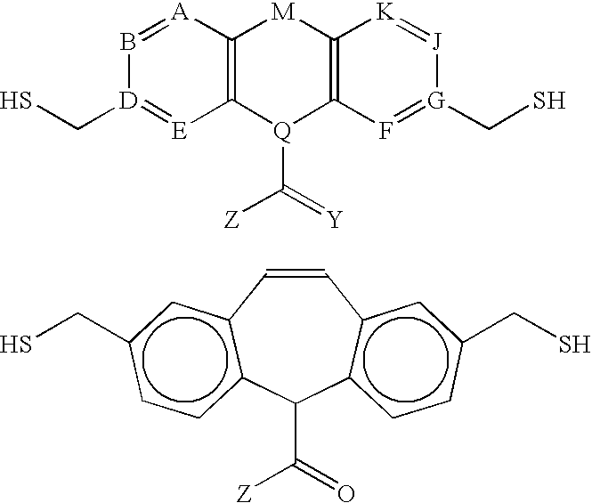


Priority Applications (6)
| Application Number | Priority Date | Filing Date | Title |
|---|---|---|---|
| US10/187,721 US7186380B2 (en) | 2002-07-01 | 2002-07-01 | Transistor and sensors made from molecular materials with electric dipoles |
| KR1020047021718A KR101015759B1 (en) | 2002-07-01 | 2003-06-26 | Transistor and sensors made from molecular materials with electric dipoles |
| AU2003263755A AU2003263755A1 (en) | 2002-07-01 | 2003-06-26 | Transistor and sensors made from molecular materials with electric dipoles |
| EP03762044A EP1518280A2 (en) | 2002-07-01 | 2003-06-26 | Transistor and sensors made from molecular materials with electric dipoles |
| JP2004517827A JP2005533371A (en) | 2002-07-01 | 2003-06-26 | Transistor and sensor made of molecular material with electric dipole |
| PCT/US2003/020068 WO2004003972A2 (en) | 2002-07-01 | 2003-06-26 | Transistor and sensors made from molecular materials with electric dipoles |
Applications Claiming Priority (1)
| Application Number | Priority Date | Filing Date | Title |
|---|---|---|---|
| US10/187,721 US7186380B2 (en) | 2002-07-01 | 2002-07-01 | Transistor and sensors made from molecular materials with electric dipoles |
Publications (2)
| Publication Number | Publication Date |
|---|---|
| US20040001778A1 true US20040001778A1 (en) | 2004-01-01 |
| US7186380B2 US7186380B2 (en) | 2007-03-06 |
Family
ID=29780066
Family Applications (1)
| Application Number | Title | Priority Date | Filing Date |
|---|---|---|---|
| US10/187,721 Expired - Fee Related US7186380B2 (en) | 2002-07-01 | 2002-07-01 | Transistor and sensors made from molecular materials with electric dipoles |
Country Status (6)
| Country | Link |
|---|---|
| US (1) | US7186380B2 (en) |
| EP (1) | EP1518280A2 (en) |
| JP (1) | JP2005533371A (en) |
| KR (1) | KR101015759B1 (en) |
| AU (1) | AU2003263755A1 (en) |
| WO (1) | WO2004003972A2 (en) |
Cited By (25)
| Publication number | Priority date | Publication date | Assignee | Title |
|---|---|---|---|---|
| US20040012062A1 (en) * | 2002-07-19 | 2004-01-22 | Matsushita Electric Works, Ltd. | Mechanical deformation amount sensor |
| US20050093425A1 (en) * | 2002-08-01 | 2005-05-05 | Sanyo Electric Co., Ltd | Optical sensor, method of manufacturing and driving an optical sensor, method of detecting light intensity |
| US20050127461A1 (en) * | 2003-11-25 | 2005-06-16 | Dey Sandwip K. | Molecular modifications of metal/dielectric interfaces |
| US20050205861A1 (en) * | 2004-03-17 | 2005-09-22 | Lucent Technologies Inc. | P-type OFET with fluorinated channels |
| US20050274609A1 (en) * | 2004-05-18 | 2005-12-15 | Yong Chen | Composition of matter which results in electronic switching through intra- or inter- molecular charge transfer, or charge transfer between molecules and electrodes induced by an electrical field |
| WO2006004952A1 (en) * | 2004-06-30 | 2006-01-12 | Hewlett-Packard Development Company L.P. | Molecules for langmuir-blodgett deposition of a molecular layer |
| US20060102889A1 (en) * | 2004-11-18 | 2006-05-18 | Electronics And Telecommunications Research Institute | Tri-gated molecular field effect transistor and method of fabricating the same |
| FR2886459A1 (en) * | 2005-05-31 | 2006-12-01 | Thales Sa | NETWORK OF NANOTUBE OR NANOFIL SEMICONDUCTOR FET TRANSISTORS AND CORRESPONDING ELECTRONIC DEVICE FOR THE DETECTION OF ANALYTES |
| US20060284543A1 (en) * | 2005-06-18 | 2006-12-21 | Chung Deuk-Seok | Ferroelectric cold cathode and ferroelectric field emission device including the ferroelectric cold cathode |
| US20080102213A1 (en) * | 2006-01-03 | 2008-05-01 | International Business Machines Corporation | Selective placement of carbon nanotubes through functionalization |
| US20080229839A1 (en) * | 2007-03-21 | 2008-09-25 | Rosemount Inc. | Sensor with composite diaphragm containing carbon nanotubes or semiconducting nanowires |
| EP2239561A1 (en) | 2009-04-09 | 2010-10-13 | Technische Universität Graz | OFET-based sensor for detecting an analyte |
| CN101893494A (en) * | 2010-08-13 | 2010-11-24 | 武汉大学 | Zinc oxide nano-rod pressure sensor and manufacturing method thereof |
| CN102099673A (en) * | 2008-01-28 | 2011-06-15 | 罗伯特.博世有限公司 | Sensor element of a gas sensor |
| WO2014045274A1 (en) * | 2012-09-24 | 2014-03-27 | Ben Gurion University Of The Negev Research And Development Authority | Bilayer graphene diode |
| US8704321B2 (en) | 2009-11-05 | 2014-04-22 | Panasonic Corporation | Solid-state imaging device |
| US8945912B2 (en) | 2008-09-29 | 2015-02-03 | The Board Of Trustees Of The University Of Illinois | DNA sequencing and amplification systems using nanoscale field effect sensor arrays |
| US20150102283A1 (en) * | 2003-08-29 | 2015-04-16 | Japan Science And Technology Agency | Field-effect transistor, single-electron transistor and sensor using the same |
| WO2015121534A1 (en) * | 2014-02-17 | 2015-08-20 | Nokia Technologies Oy | Field-effect sensor and associated methods |
| US20170146483A1 (en) * | 2014-06-03 | 2017-05-25 | The Regents Of The University Of California | Chemically sensitive field effect transistor sensors |
| WO2017171851A1 (en) * | 2016-04-01 | 2017-10-05 | Intel Corporation | Ferroelectric-based field-effect transistor with threshold voltage switching for enhanced on-state and off-state performance |
| TWI612642B (en) * | 2015-10-20 | 2018-01-21 | 國立研究開發法人產業技術總合研究所 | Non-volatile storage element |
| JP2021005644A (en) * | 2019-06-26 | 2021-01-14 | 国立大学法人広島大学 | Field effect transistor and memory device |
| US11232832B2 (en) * | 2016-04-01 | 2022-01-25 | Intel Corporation | Polarization gate stack SRAM |
| US11469323B2 (en) | 2018-09-25 | 2022-10-11 | Intel Corporation | Ferroelectric gate stack for band-to-band tunneling reduction |
Families Citing this family (21)
| Publication number | Priority date | Publication date | Assignee | Title |
|---|---|---|---|---|
| US7247877B2 (en) * | 2004-08-20 | 2007-07-24 | International Business Machines Corporation | Integrated carbon nanotube sensors |
| JP4745652B2 (en) * | 2004-11-30 | 2011-08-10 | シャープ株式会社 | Semiconductor device |
| DE102005017533A1 (en) * | 2004-12-29 | 2006-07-13 | Hynix Semiconductor Inc., Ichon | Nonvolatile ferroelectric memory device e.g. ferroelectric random access memory device, has ferroelectric layer formed on floating channel layer and word line formed on ferroelectric layer |
| JP4727287B2 (en) * | 2005-04-27 | 2011-07-20 | 日本電信電話株式会社 | Molecular control method |
| KR100966301B1 (en) * | 2005-05-11 | 2010-06-28 | 서울시립대학교 산학협력단 | Manufacturing method of ferroelectric Memory Device |
| JP2007096129A (en) * | 2005-09-29 | 2007-04-12 | Kyoto Univ | Molecule transistor, and method for manufacturing the same and nonvolatile memory and piezoelectric sensor using the same method |
| JP2008042102A (en) * | 2006-08-10 | 2008-02-21 | Kyoto Univ | Ferroelectric memory |
| US8030637B2 (en) * | 2006-08-25 | 2011-10-04 | Qimonda Ag | Memory element using reversible switching between SP2 and SP3 hybridized carbon |
| US7960776B2 (en) * | 2006-09-27 | 2011-06-14 | Cornell Research Foundation, Inc. | Transistor with floating gate and electret |
| US20080102278A1 (en) | 2006-10-27 | 2008-05-01 | Franz Kreupl | Carbon filament memory and method for fabrication |
| US7915603B2 (en) * | 2006-10-27 | 2011-03-29 | Qimonda Ag | Modifiable gate stack memory element |
| KR100866314B1 (en) * | 2006-12-13 | 2008-11-03 | 서울시립대학교 산학협력단 | MFMS FET and ferroelectric memory device |
| KR101143706B1 (en) * | 2008-09-24 | 2012-05-09 | 인터내셔널 비지네스 머신즈 코포레이션 | Nanoelectronic device |
| KR20100094192A (en) * | 2009-02-18 | 2010-08-26 | 삼성전자주식회사 | Static random access memory using carbon nanotube thin films |
| TWI394948B (en) * | 2009-03-17 | 2013-05-01 | Univ Nat Chiao Tung | Label-free sensor |
| JP6122854B2 (en) * | 2011-09-29 | 2017-04-26 | インテル・コーポレーション | Method for manufacturing a substrate having a metal layer |
| ITMI20122041A1 (en) | 2012-11-29 | 2014-05-30 | Dhitech Distretto Tecnologico H Igh Tech S C A R | ELECTRONIC DEVICE FOR THE REALIZATION OF DIGITAL FUNCTIONS BY MOLECULAR FUNCTIONAL ELEMENTS. |
| US11476353B2 (en) * | 2016-11-21 | 2022-10-18 | The Government Of The United States Of America, As Represented By The Secretary Of The Navy | Lateral heterojunctions in two-dimensional materials integrated with multiferroic layers |
| KR102116655B1 (en) * | 2018-12-03 | 2020-06-01 | 연세대학교 산학협력단 | Oxide semiconductor thin film transistor |
| KR102399039B1 (en) * | 2020-06-19 | 2022-05-16 | 성균관대학교산학협력단 | Sensor for monitoring 3D-cultured cell or tissue and Method for fabricating the same based on roll-to-roll process |
| JP7450928B2 (en) * | 2020-07-29 | 2024-03-18 | 国立大学法人広島大学 | Monomolecular dielectric film and method for producing monomolecular dielectric film |
Citations (8)
| Publication number | Priority date | Publication date | Assignee | Title |
|---|---|---|---|---|
| US5034608A (en) * | 1989-09-08 | 1991-07-23 | Massachusetts Institute Of Technology | Infrared sensor operable without cooling |
| US5471069A (en) * | 1990-10-31 | 1995-11-28 | Sumitomo Electric Industries, Ltd. | Superconducting device having an extremely short superconducting channel formed of extremely thin oxide superconductor film |
| US5864161A (en) * | 1994-09-13 | 1999-01-26 | Kabushiki Kaisha Toshiba | Semiconductor device and manufacturing method thereof |
| US20020075420A1 (en) * | 2000-12-14 | 2002-06-20 | Xiao-An Zhang | Molecular devices activated by an electric field for electronic ink and other visual display |
| US20040238814A1 (en) * | 2001-12-25 | 2004-12-02 | Masanobu Mizusaki | Transistor and display device including the transistor |
| US20050023522A1 (en) * | 2001-11-07 | 2005-02-03 | Gitti Frey | Organic field effect transistors |
| US6858162B2 (en) * | 2002-04-01 | 2005-02-22 | Hewlett-Packard Development Company, L.P. | Single molecule realization of the switch and doide combination |
| US20050062097A1 (en) * | 2001-12-14 | 2005-03-24 | Veena Misra | Method and system for molecular charge storage field effect transistor |
Family Cites Families (7)
| Publication number | Priority date | Publication date | Assignee | Title |
|---|---|---|---|---|
| GB1572181A (en) | 1975-08-18 | 1980-07-23 | Ici Ltd | Device comprising a thin film of organic materila |
| JPH0766991B2 (en) * | 1990-04-27 | 1995-07-19 | 松下電器産業株式会社 | Electric control element |
| JPH03222476A (en) * | 1990-01-29 | 1991-10-01 | Matsushita Electric Ind Co Ltd | Electric control cell |
| JPH03262170A (en) * | 1990-03-13 | 1991-11-21 | Toshiba Corp | Organic/inorganic junction type semiconductor element |
| JP3150331B2 (en) * | 1990-09-28 | 2001-03-26 | 株式会社東芝 | Organic thin film element |
| US6459095B1 (en) | 1999-03-29 | 2002-10-01 | Hewlett-Packard Company | Chemically synthesized and assembled electronics devices |
| JP4178904B2 (en) * | 2002-10-16 | 2008-11-12 | アンデン株式会社 | Power element temperature protection device |
-
2002
- 2002-07-01 US US10/187,721 patent/US7186380B2/en not_active Expired - Fee Related
-
2003
- 2003-06-26 KR KR1020047021718A patent/KR101015759B1/en not_active IP Right Cessation
- 2003-06-26 EP EP03762044A patent/EP1518280A2/en not_active Withdrawn
- 2003-06-26 JP JP2004517827A patent/JP2005533371A/en active Pending
- 2003-06-26 WO PCT/US2003/020068 patent/WO2004003972A2/en active Application Filing
- 2003-06-26 AU AU2003263755A patent/AU2003263755A1/en not_active Abandoned
Patent Citations (8)
| Publication number | Priority date | Publication date | Assignee | Title |
|---|---|---|---|---|
| US5034608A (en) * | 1989-09-08 | 1991-07-23 | Massachusetts Institute Of Technology | Infrared sensor operable without cooling |
| US5471069A (en) * | 1990-10-31 | 1995-11-28 | Sumitomo Electric Industries, Ltd. | Superconducting device having an extremely short superconducting channel formed of extremely thin oxide superconductor film |
| US5864161A (en) * | 1994-09-13 | 1999-01-26 | Kabushiki Kaisha Toshiba | Semiconductor device and manufacturing method thereof |
| US20020075420A1 (en) * | 2000-12-14 | 2002-06-20 | Xiao-An Zhang | Molecular devices activated by an electric field for electronic ink and other visual display |
| US20050023522A1 (en) * | 2001-11-07 | 2005-02-03 | Gitti Frey | Organic field effect transistors |
| US20050062097A1 (en) * | 2001-12-14 | 2005-03-24 | Veena Misra | Method and system for molecular charge storage field effect transistor |
| US20040238814A1 (en) * | 2001-12-25 | 2004-12-02 | Masanobu Mizusaki | Transistor and display device including the transistor |
| US6858162B2 (en) * | 2002-04-01 | 2005-02-22 | Hewlett-Packard Development Company, L.P. | Single molecule realization of the switch and doide combination |
Cited By (45)
| Publication number | Priority date | Publication date | Assignee | Title |
|---|---|---|---|---|
| US6848320B2 (en) * | 2002-07-19 | 2005-02-01 | Matsushita Electric Works, Ltd. | Mechanical deformation amount sensor |
| US20040012062A1 (en) * | 2002-07-19 | 2004-01-22 | Matsushita Electric Works, Ltd. | Mechanical deformation amount sensor |
| US20050093425A1 (en) * | 2002-08-01 | 2005-05-05 | Sanyo Electric Co., Ltd | Optical sensor, method of manufacturing and driving an optical sensor, method of detecting light intensity |
| US9506892B2 (en) * | 2003-08-29 | 2016-11-29 | Japan Science And Technology Agency | Field-effect transistor, single-electron transistor and sensor using the same |
| US20150102283A1 (en) * | 2003-08-29 | 2015-04-16 | Japan Science And Technology Agency | Field-effect transistor, single-electron transistor and sensor using the same |
| US20050127461A1 (en) * | 2003-11-25 | 2005-06-16 | Dey Sandwip K. | Molecular modifications of metal/dielectric interfaces |
| US7510942B2 (en) * | 2003-11-25 | 2009-03-31 | Arizona Board Of Regents, Acting For And On Behalf Of Arizona State University | Molecular modifications of metal/dielectric interfaces |
| US20050205861A1 (en) * | 2004-03-17 | 2005-09-22 | Lucent Technologies Inc. | P-type OFET with fluorinated channels |
| US7057205B2 (en) * | 2004-03-17 | 2006-06-06 | Lucent Technologies Inc. | P-type OFET with fluorinated channels |
| US20050274609A1 (en) * | 2004-05-18 | 2005-12-15 | Yong Chen | Composition of matter which results in electronic switching through intra- or inter- molecular charge transfer, or charge transfer between molecules and electrodes induced by an electrical field |
| WO2006004952A1 (en) * | 2004-06-30 | 2006-01-12 | Hewlett-Packard Development Company L.P. | Molecules for langmuir-blodgett deposition of a molecular layer |
| US20060102889A1 (en) * | 2004-11-18 | 2006-05-18 | Electronics And Telecommunications Research Institute | Tri-gated molecular field effect transistor and method of fabricating the same |
| US7436033B2 (en) | 2004-11-18 | 2008-10-14 | Electronics And Telecommunications Research Institute | Tri-gated molecular field effect transistor and method of fabricating the same |
| FR2886459A1 (en) * | 2005-05-31 | 2006-12-01 | Thales Sa | NETWORK OF NANOTUBE OR NANOFIL SEMICONDUCTOR FET TRANSISTORS AND CORRESPONDING ELECTRONIC DEVICE FOR THE DETECTION OF ANALYTES |
| WO2006128828A1 (en) * | 2005-05-31 | 2006-12-07 | Thales | Conductive nanotube or nanowire fet transistor network and corresponding electronic device, for detecting analytes |
| US8115198B2 (en) | 2005-05-31 | 2012-02-14 | Thales and Ecole Polytechnique | Array of differentiated FETS having a nanotube or nanowire channel and corresponding electronic device, for the detection of analytes |
| US20060284543A1 (en) * | 2005-06-18 | 2006-12-21 | Chung Deuk-Seok | Ferroelectric cold cathode and ferroelectric field emission device including the ferroelectric cold cathode |
| US8084012B2 (en) | 2006-01-03 | 2011-12-27 | International Business Machines Corporation | Selective placement of carbon nanotubes through functionalization |
| US8859048B2 (en) * | 2006-01-03 | 2014-10-14 | International Business Machines Corporation | Selective placement of carbon nanotubes through functionalization |
| US20100145034A1 (en) * | 2006-01-03 | 2010-06-10 | International Business Machines Corporation | Selective placement of carbon nanotubes through functionalization |
| US20080102213A1 (en) * | 2006-01-03 | 2008-05-01 | International Business Machines Corporation | Selective placement of carbon nanotubes through functionalization |
| US8283453B2 (en) | 2006-01-03 | 2012-10-09 | International Business Machines Corporation | Selective placement of carbon nanotubes through functionalization |
| WO2008143720A2 (en) | 2007-03-21 | 2008-11-27 | Rosemount Inc. | Sensor with composite diaphragm containing carbon nanotubes or semiconducting nanowires |
| US7437938B2 (en) | 2007-03-21 | 2008-10-21 | Rosemount Inc. | Sensor with composite diaphragm containing carbon nanotubes or semiconducting nanowires |
| US20080229839A1 (en) * | 2007-03-21 | 2008-09-25 | Rosemount Inc. | Sensor with composite diaphragm containing carbon nanotubes or semiconducting nanowires |
| CN102099673A (en) * | 2008-01-28 | 2011-06-15 | 罗伯特.博世有限公司 | Sensor element of a gas sensor |
| US8945912B2 (en) | 2008-09-29 | 2015-02-03 | The Board Of Trustees Of The University Of Illinois | DNA sequencing and amplification systems using nanoscale field effect sensor arrays |
| EP2239561A1 (en) | 2009-04-09 | 2010-10-13 | Technische Universität Graz | OFET-based sensor for detecting an analyte |
| US8704321B2 (en) | 2009-11-05 | 2014-04-22 | Panasonic Corporation | Solid-state imaging device |
| CN101893494A (en) * | 2010-08-13 | 2010-11-24 | 武汉大学 | Zinc oxide nano-rod pressure sensor and manufacturing method thereof |
| WO2014045274A1 (en) * | 2012-09-24 | 2014-03-27 | Ben Gurion University Of The Negev Research And Development Authority | Bilayer graphene diode |
| WO2015121534A1 (en) * | 2014-02-17 | 2015-08-20 | Nokia Technologies Oy | Field-effect sensor and associated methods |
| US20170176380A1 (en) * | 2014-02-17 | 2017-06-22 | Nokia Technologies Oy | Field-effect sensor and associated methods |
| CN106233481A (en) * | 2014-02-17 | 2016-12-14 | 诺基亚技术有限公司 | Field effect transistor and the method being associated |
| US9989488B2 (en) * | 2014-02-17 | 2018-06-05 | Nokia Technologies Oy | Field-effect sensor and associated methods |
| US10330637B2 (en) * | 2014-06-03 | 2019-06-25 | The Regents Of The University Of California | Chemically sensitive field effect transistor sensors |
| US20170146483A1 (en) * | 2014-06-03 | 2017-05-25 | The Regents Of The University Of California | Chemically sensitive field effect transistor sensors |
| TWI612642B (en) * | 2015-10-20 | 2018-01-21 | 國立研究開發法人產業技術總合研究所 | Non-volatile storage element |
| US10256288B2 (en) | 2015-10-20 | 2019-04-09 | National Institute Of Advanced Industrial Science And Technology | Nonvolatile memory device |
| WO2017171851A1 (en) * | 2016-04-01 | 2017-10-05 | Intel Corporation | Ferroelectric-based field-effect transistor with threshold voltage switching for enhanced on-state and off-state performance |
| US10720505B2 (en) | 2016-04-01 | 2020-07-21 | Intel Corporation | Ferroelectric-based field-effect transistor with threshold voltage switching for enhanced on-state and off-state performance |
| US11232832B2 (en) * | 2016-04-01 | 2022-01-25 | Intel Corporation | Polarization gate stack SRAM |
| US11476345B2 (en) * | 2016-04-01 | 2022-10-18 | Intel Corporation | Ferroelectric-based field-effect transistor with threshold voltage switching for enhanced on-state and off-state performance |
| US11469323B2 (en) | 2018-09-25 | 2022-10-11 | Intel Corporation | Ferroelectric gate stack for band-to-band tunneling reduction |
| JP2021005644A (en) * | 2019-06-26 | 2021-01-14 | 国立大学法人広島大学 | Field effect transistor and memory device |
Also Published As
| Publication number | Publication date |
|---|---|
| KR101015759B1 (en) | 2011-02-22 |
| AU2003263755A1 (en) | 2004-01-19 |
| JP2005533371A (en) | 2005-11-04 |
| WO2004003972A3 (en) | 2004-07-08 |
| AU2003263755A8 (en) | 2004-01-19 |
| EP1518280A2 (en) | 2005-03-30 |
| US7186380B2 (en) | 2007-03-06 |
| WO2004003972A2 (en) | 2004-01-08 |
| KR20050024458A (en) | 2005-03-10 |
Similar Documents
| Publication | Publication Date | Title |
|---|---|---|
| US7186380B2 (en) | Transistor and sensors made from molecular materials with electric dipoles | |
| US8471298B2 (en) | Nanoscopic wire-based devices and arrays | |
| JP5810103B2 (en) | Semiconductor device including electro-permeable source layer and method of manufacturing the same | |
| Ouyang et al. | Organic memory device fabricated through solution processing | |
| Chen et al. | Graphene and its derivatives: switching ON and OFF | |
| US6559468B1 (en) | Molecular wire transistor (MWT) | |
| US6911682B2 (en) | Electromechanical three-trace junction devices | |
| JP4499418B2 (en) | Method for manufacturing a molecular electronic device | |
| EP1500110B1 (en) | Molecular wire crossbar flash memory | |
| EP2092528B1 (en) | Memory device and method for fabricating a memory device | |
| Dongale et al. | Shifting towards nanoelectronics: A device level overview | |
| Ruhee et al. | Visions for a molecular future | |
| Chakraborty et al. | Brace of Nanowire FETs in the Advancements and Miniaturizations of Recent Integrated Circuits Design | |
| AU2006202493B2 (en) | Nanoscopic wire-based devices, arrays, and methods of their manufacture | |
| AU2005201840B2 (en) | Nanoscopic wire-based devices, arrays, and methods of their manufacture | |
| Hornyak et al. | Nanoelectronics | |
| Kornilovitch | Molecular Electronics and Resistance of Molecule-Metal Interfaces |
Legal Events
| Date | Code | Title | Description |
|---|---|---|---|
| AS | Assignment |
Owner name: HEWLETT-PACKARD COMPANY, COLORADO Free format text: ASSIGNMENT OF ASSIGNORS INTEREST;ASSIGNORS:CHEN, YONG;BRATKOVSKI, ALEXANDRE M.;WILLIAMS, R. STANLEY;REEL/FRAME:013539/0571 Effective date: 20020628 |
|
| AS | Assignment |
Owner name: HEWLETT-PACKARD DEVELOPMENT COMPANY, L.P., COLORAD Free format text: ASSIGNMENT OF ASSIGNORS INTEREST;ASSIGNOR:HEWLETT-PACKARD COMPANY;REEL/FRAME:013776/0928 Effective date: 20030131 Owner name: HEWLETT-PACKARD DEVELOPMENT COMPANY, L.P.,COLORADO Free format text: ASSIGNMENT OF ASSIGNORS INTEREST;ASSIGNOR:HEWLETT-PACKARD COMPANY;REEL/FRAME:013776/0928 Effective date: 20030131 |
|
| AS | Assignment |
Owner name: HEWLETT-PACKARD DEVELOPMENT COMPANY L.P., TEXAS Free format text: ASSIGNMENT OF ASSIGNORS INTEREST;ASSIGNOR:HEWLETT-PACKARD COMPANY;REEL/FRAME:014061/0492 Effective date: 20030926 Owner name: HEWLETT-PACKARD DEVELOPMENT COMPANY L.P.,TEXAS Free format text: ASSIGNMENT OF ASSIGNORS INTEREST;ASSIGNOR:HEWLETT-PACKARD COMPANY;REEL/FRAME:014061/0492 Effective date: 20030926 |
|
| CC | Certificate of correction | ||
| FPAY | Fee payment |
Year of fee payment: 4 |
|
| REMI | Maintenance fee reminder mailed | ||
| LAPS | Lapse for failure to pay maintenance fees | ||
| STCH | Information on status: patent discontinuation |
Free format text: PATENT EXPIRED DUE TO NONPAYMENT OF MAINTENANCE FEES UNDER 37 CFR 1.362 |
|
| FP | Lapsed due to failure to pay maintenance fee |
Effective date: 20150306 |