US20030198065A1 - Inverter having self adjusting output frequency for use with other inverters in parallel - Google Patents
Inverter having self adjusting output frequency for use with other inverters in parallel Download PDFInfo
- Publication number
- US20030198065A1 US20030198065A1 US10/457,722 US45772203A US2003198065A1 US 20030198065 A1 US20030198065 A1 US 20030198065A1 US 45772203 A US45772203 A US 45772203A US 2003198065 A1 US2003198065 A1 US 2003198065A1
- Authority
- US
- United States
- Prior art keywords
- sine wave
- phase angle
- power
- wave reference
- output
- Prior art date
- Legal status (The legal status is an assumption and is not a legal conclusion. Google has not performed a legal analysis and makes no representation as to the accuracy of the status listed.)
- Granted
Links
Images


Classifications
-
- H—ELECTRICITY
- H02—GENERATION; CONVERSION OR DISTRIBUTION OF ELECTRIC POWER
- H02M—APPARATUS FOR CONVERSION BETWEEN AC AND AC, BETWEEN AC AND DC, OR BETWEEN DC AND DC, AND FOR USE WITH MAINS OR SIMILAR POWER SUPPLY SYSTEMS; CONVERSION OF DC OR AC INPUT POWER INTO SURGE OUTPUT POWER; CONTROL OR REGULATION THEREOF
- H02M7/00—Conversion of AC power input into DC power output; Conversion of DC power input into AC power output
- H02M7/42—Conversion of DC power input into AC power output without possibility of reversal
- H02M7/44—Conversion of DC power input into AC power output without possibility of reversal by static converters
- H02M7/48—Conversion of DC power input into AC power output without possibility of reversal by static converters using discharge tubes with control electrode or semiconductor devices with control electrode
- H02M7/493—Conversion of DC power input into AC power output without possibility of reversal by static converters using discharge tubes with control electrode or semiconductor devices with control electrode the static converters being arranged for operation in parallel
-
- H—ELECTRICITY
- H02—GENERATION; CONVERSION OR DISTRIBUTION OF ELECTRIC POWER
- H02M—APPARATUS FOR CONVERSION BETWEEN AC AND AC, BETWEEN AC AND DC, OR BETWEEN DC AND DC, AND FOR USE WITH MAINS OR SIMILAR POWER SUPPLY SYSTEMS; CONVERSION OF DC OR AC INPUT POWER INTO SURGE OUTPUT POWER; CONTROL OR REGULATION THEREOF
- H02M5/00—Conversion of AC power input into AC power output, e.g. for change of voltage, for change of frequency, for change of number of phases
- H02M5/40—Conversion of AC power input into AC power output, e.g. for change of voltage, for change of frequency, for change of number of phases with intermediate conversion into DC
- H02M5/42—Conversion of AC power input into AC power output, e.g. for change of voltage, for change of frequency, for change of number of phases with intermediate conversion into DC by static converters
- H02M5/44—Conversion of AC power input into AC power output, e.g. for change of voltage, for change of frequency, for change of number of phases with intermediate conversion into DC by static converters using discharge tubes or semiconductor devices to convert the intermediate DC into AC
- H02M5/443—Conversion of AC power input into AC power output, e.g. for change of voltage, for change of frequency, for change of number of phases with intermediate conversion into DC by static converters using discharge tubes or semiconductor devices to convert the intermediate DC into AC using devices of a thyratron or thyristor type requiring extinguishing means
- H02M5/45—Conversion of AC power input into AC power output, e.g. for change of voltage, for change of frequency, for change of number of phases with intermediate conversion into DC by static converters using discharge tubes or semiconductor devices to convert the intermediate DC into AC using devices of a thyratron or thyristor type requiring extinguishing means using semiconductor devices only
- H02M5/4505—Conversion of AC power input into AC power output, e.g. for change of voltage, for change of frequency, for change of number of phases with intermediate conversion into DC by static converters using discharge tubes or semiconductor devices to convert the intermediate DC into AC using devices of a thyratron or thyristor type requiring extinguishing means using semiconductor devices only having a rectifier with controlled elements
-
- H—ELECTRICITY
- H02—GENERATION; CONVERSION OR DISTRIBUTION OF ELECTRIC POWER
- H02M—APPARATUS FOR CONVERSION BETWEEN AC AND AC, BETWEEN AC AND DC, OR BETWEEN DC AND DC, AND FOR USE WITH MAINS OR SIMILAR POWER SUPPLY SYSTEMS; CONVERSION OF DC OR AC INPUT POWER INTO SURGE OUTPUT POWER; CONTROL OR REGULATION THEREOF
- H02M5/00—Conversion of AC power input into AC power output, e.g. for change of voltage, for change of frequency, for change of number of phases
- H02M5/40—Conversion of AC power input into AC power output, e.g. for change of voltage, for change of frequency, for change of number of phases with intermediate conversion into DC
- H02M5/42—Conversion of AC power input into AC power output, e.g. for change of voltage, for change of frequency, for change of number of phases with intermediate conversion into DC by static converters
- H02M5/44—Conversion of AC power input into AC power output, e.g. for change of voltage, for change of frequency, for change of number of phases with intermediate conversion into DC by static converters using discharge tubes or semiconductor devices to convert the intermediate DC into AC
- H02M5/443—Conversion of AC power input into AC power output, e.g. for change of voltage, for change of frequency, for change of number of phases with intermediate conversion into DC by static converters using discharge tubes or semiconductor devices to convert the intermediate DC into AC using devices of a thyratron or thyristor type requiring extinguishing means
- H02M5/45—Conversion of AC power input into AC power output, e.g. for change of voltage, for change of frequency, for change of number of phases with intermediate conversion into DC by static converters using discharge tubes or semiconductor devices to convert the intermediate DC into AC using devices of a thyratron or thyristor type requiring extinguishing means using semiconductor devices only
- H02M5/451—Conversion of AC power input into AC power output, e.g. for change of voltage, for change of frequency, for change of number of phases with intermediate conversion into DC by static converters using discharge tubes or semiconductor devices to convert the intermediate DC into AC using devices of a thyratron or thyristor type requiring extinguishing means using semiconductor devices only with automatic control of output voltage or frequency
-
- H—ELECTRICITY
- H02—GENERATION; CONVERSION OR DISTRIBUTION OF ELECTRIC POWER
- H02M—APPARATUS FOR CONVERSION BETWEEN AC AND AC, BETWEEN AC AND DC, OR BETWEEN DC AND DC, AND FOR USE WITH MAINS OR SIMILAR POWER SUPPLY SYSTEMS; CONVERSION OF DC OR AC INPUT POWER INTO SURGE OUTPUT POWER; CONTROL OR REGULATION THEREOF
- H02M5/00—Conversion of AC power input into AC power output, e.g. for change of voltage, for change of frequency, for change of number of phases
- H02M5/40—Conversion of AC power input into AC power output, e.g. for change of voltage, for change of frequency, for change of number of phases with intermediate conversion into DC
- H02M5/42—Conversion of AC power input into AC power output, e.g. for change of voltage, for change of frequency, for change of number of phases with intermediate conversion into DC by static converters
- H02M5/44—Conversion of AC power input into AC power output, e.g. for change of voltage, for change of frequency, for change of number of phases with intermediate conversion into DC by static converters using discharge tubes or semiconductor devices to convert the intermediate DC into AC
- H02M5/453—Conversion of AC power input into AC power output, e.g. for change of voltage, for change of frequency, for change of number of phases with intermediate conversion into DC by static converters using discharge tubes or semiconductor devices to convert the intermediate DC into AC using devices of a triode or transistor type requiring continuous application of a control signal
- H02M5/458—Conversion of AC power input into AC power output, e.g. for change of voltage, for change of frequency, for change of number of phases with intermediate conversion into DC by static converters using discharge tubes or semiconductor devices to convert the intermediate DC into AC using devices of a triode or transistor type requiring continuous application of a control signal using semiconductor devices only
- H02M5/4585—Conversion of AC power input into AC power output, e.g. for change of voltage, for change of frequency, for change of number of phases with intermediate conversion into DC by static converters using discharge tubes or semiconductor devices to convert the intermediate DC into AC using devices of a triode or transistor type requiring continuous application of a control signal using semiconductor devices only having a rectifier with controlled elements
-
- H—ELECTRICITY
- H02—GENERATION; CONVERSION OR DISTRIBUTION OF ELECTRIC POWER
- H02P—CONTROL OR REGULATION OF ELECTRIC MOTORS, ELECTRIC GENERATORS OR DYNAMO-ELECTRIC CONVERTERS; CONTROLLING TRANSFORMERS, REACTORS OR CHOKE COILS
- H02P9/00—Arrangements for controlling electric generators for the purpose of obtaining a desired output
- H02P9/14—Arrangements for controlling electric generators for the purpose of obtaining a desired output by variation of field
- H02P9/26—Arrangements for controlling electric generators for the purpose of obtaining a desired output by variation of field using discharge tubes or semiconductor devices
- H02P9/30—Arrangements for controlling electric generators for the purpose of obtaining a desired output by variation of field using discharge tubes or semiconductor devices using semiconductor devices
- H02P9/305—Arrangements for controlling electric generators for the purpose of obtaining a desired output by variation of field using discharge tubes or semiconductor devices using semiconductor devices controlling voltage
-
- H—ELECTRICITY
- H02—GENERATION; CONVERSION OR DISTRIBUTION OF ELECTRIC POWER
- H02M—APPARATUS FOR CONVERSION BETWEEN AC AND AC, BETWEEN AC AND DC, OR BETWEEN DC AND DC, AND FOR USE WITH MAINS OR SIMILAR POWER SUPPLY SYSTEMS; CONVERSION OF DC OR AC INPUT POWER INTO SURGE OUTPUT POWER; CONTROL OR REGULATION THEREOF
- H02M1/00—Details of apparatus for conversion
- H02M1/0083—Converters characterised by their input or output configuration
- H02M1/0085—Partially controlled bridges
Definitions
- This invention relates to an inverter suitable for use with portable AC power supply units.
- Inverters have been incorporated in portable AC power supply units, drivers of AC motors, uninterruptable power supply units, etc.
- portable AC power supply units As one of modes of application, a plurality of, for example, two portable AC power supply units are connected in parallel with each other to drive a load. In this case, the portable AC power supply units are operated with output frequencies in synchronism with each other. Current (cross current) flows from one of the power supply units to the other when a change in the load etc. results in a subtle change in the frequency of either power supply unit. The cross current sometimes breaks circuit components of the portable AC power supply unit. The cross current flows from the power supply unit with a higher output frequency to the one with a lower output frequency.
- a portable AC power supply unit 1 comprises an engine drive AC generator 2 and an inverter unit 3 having output terminals 3 a and 3 b from which a sinusoidal AC voltage is delivered.
- the inverter unit 3 includes a rectifier circuit 4 rectifying a three-phase AC voltage generated by the AC generator 2 , a smoothing capacitor 5 , a single-phase full-bridge inverter circuit 6 , a filter circuit 7 , a control circuit 8 and a drive circuit 9 .
- the control circuit 8 includes a microcomputer 10 and a pulse-width-modulation (PWM) circuit 11 generating a drive signal.
- PWM pulse-width-modulation
- the inverter circuit 6 is adapted to be connected to a load. When a plurality of the portable AC power supply units 1 are to be connected to each other, the inverter circuits 6 of the respective power supply units 1 are connected to each other.
- the control circuit 8 controls the generator 2 so that the engine maintains a predetermined number of revolution.
- the control circuit 8 further performs a PWM control so that a sine wave AC voltage having a predetermined voltage (for example, an effective value of 100V) at a predetermined frequency (50 Hz or 60 Hz) is delivered from the output terminals 3 a and 3 b .
- the control circuit 8 further includes an output voltage detecting circuit 12 detecting an output voltage of the inverter circuit 6 , an output current detecting circuit 13 detecting an output current of the inverter circuit 6 and a phase difference detecting circuit 14 detecting a phase difference between the output voltage and the output current.
- the control circuit 8 increases an output frequency when the output current lags behind the output voltage.
- control circuit 8 decreases the output frequency when the output current leads the output voltage. Consequently, an output balance is achieved between the two AC power supply units 1 connected in parallel with each other.
- the output frequencies are adjusted in a range between 49.90 Hz and 50.10 Hz when the portable AC power supply units are of 50 Hz specification.
- the phase difference is detected by measuring a time from a zero cross point of the output voltage (AC) to a zero cross point of the output current.
- AC output voltage
- the zero crossing may occur twice or the timing of the zero crossing may not be normal.
- the output currents are not balanced between the power supply units in a parallel operation of the power supply units.
- an object of the present invention is to provide an inverter in which the output currents are balanced in the parallel operation of the power supply units.
- the present invention provides an inverter comprising a DC power supply circuit, an inverter circuit having a plurality of switching elements and switching an output of the DC power supply circuit on the basis of a PWM signal to deliver a high-frequency voltage, a filter circuit converting the high-frequency voltage to a substantially sinusoidal AC voltage, a power detector detecting an effective or wattless power of the AC power, a phase angle calculator calculating a phase angle of current relative to voltage from the detected effective or wattless power, a phase.
- phase detector detecting a leading or lagging state of the phase angle
- controller decreasing a frequency of the output voltage when the phase detector detects the leading state of the phase angle, the controller increasing the frequency of the output voltage when the phase detector detects the lagging state of the phase angle.
- the effective power or wattless power contains a phase angle element between the output voltage and the output current.
- the effective or wattless power is detected, and the phase angle calculator calculates a phase angle on the basis of the detected effective or wattless power. Consequently, an accurate phase angle can be detected even when the output current or the output current detector contains a waveform distortion and accordingly, the accuracy in the detection of the phase angle can be improved.
- the phase detector detects the leading or lagging state of the calculated phase angle, and the controller decreases the frequency of the output voltage when the phase detector detects the leading state of the phase angle.
- the phase detector increases the frequency of the output voltage when the phase detector detects the lagging state of the phase angle. Consequently, an accurate frequency control can be carried out, and the output currents are balanced in the parallel operation of the power supply units.
- FIG. 1 is a circuit diagram showing an electrical arrangement of a portable AC power supply unit to which an inverter of an embodiment in accordance with the present invention is applied;
- FIG. 2 is a schematic block diagram showing functions of a microcomputer employed in the power supply unit
- FIG. 3 is a graph showing a data table of sine wave reference data
- FIG. 4 is a graph showing a sine wave reference signal and an output current detection signal
- FIG. 5 is a circuit diagram showing a part of a PWM circuit
- FIGS. 6A to 6 C show waveforms at points in the circuit of FIG. 5 respectively;
- FIGS. 7A to 7 C shows waveforms related to the PWM control
- FIG. 8 is a flowchart showing a control manner by the microcomputer
- FIG. 9 shows frequency setting data
- FIG. 10 is a flowchart showing another control manner by the microcomputer
- FIG. 11 shows a parallel operation of two portable AC power supply units with cross current due to output frequency occurring
- FIG. 12 shows a parallel operation of two portable AC power supply units with cross current due to output voltage occurring
- FIG. 13 is a flowchart showing a control manner in a second embodiment in accordance with the invention.
- FIG. 14 is a view similar to FIG. 9;
- FIGS. 15A to 15 C are waveform charts showing a third embodiment in accordance with the invention.
- FIGS. 16A to 16 D are waveform charts showing a fourth embodiment in accordance with the invention.
- FIG. 17 is a flowchart showing an overall control manner for correction in a fifth embodiment in accordance with the invention.
- FIG. 18 is a flowchart showing a control manner for correction
- FIG. 19 is a flowchart showing a control manner for correction using sine wave reference data
- FIG. 20 is a waveform chart showing an output voltage signal and an output current signal
- FIG. 21 is a flowchart showing determination of a leading or lagging state of the output current.
- FIG. 22 is a view similar to FIG. 1, showing a conventional power supply unit.
- the inverter of the invention is incorporated in a portable AC power supply unit in the embodiment.
- a portable AC power supply unit 21 generating AC power of 100 V and 50 Hz or 60 Hz, for example.
- the portable AC power supply unit 21 comprises a three-phase AC generator 22 driven by an engine (not shown) and a single-phase inverter unit 23 connected to a rear stage of the generator.
- the generator 22 includes a rotor, an armature neither of which is shown, and a stepping motor 24 controlling a flow rate of fuel (gasoline) to the engine so that a rotational speed of the engine is controlled.
- the armature has Y-connected primary windings 25 u , 25 v and 25 w wound thereon and an auxiliary winding 26 wound thereon.
- Primary winding terminals 27 u , 27 v and 27 w and auxiliary winding terminals 28 a and 28 b are connected to input terminals 29 u , 29 v and 29 w , 30 a and 30 b of the inverter unit 23 respectively.
- a rectifier circuit 33 is connected between DC power supply lines 31 and 32 .
- the rectifier circuit 33 is further connected to the input terminals 29 u , 29 v and 29 w .
- a smoothing capacitor 34 and an inverter circuit 37 are also connected between the DC power supply lines 31 and 32 .
- the inverter circuit 37 is further connected to output terminals 35 and 36 of the inverter unit 23 .
- a filter circuit 38 is connected to the inverter circuit 37 .
- the rectifier circuit 33 serves as a DC power supply circuit in the invention.
- the rectifier circuit 33 comprises thyristors 39 to 41 and diodes 42 to 44 connected into a three-phase hybrid bridge configuration.
- the inverter circuit 37 comprises transistors (switching elements) 45 to 48 and diodes 49 to 52 connected into a full bridge configuration.
- the filter circuit 38 comprises a reactor 55 and a capacitor 56 .
- the reactor 55 is interposed between the output terminal 53 of the inverter circuit 37 and the output terminal 35 of the inverter unit 23 .
- the capacitor 56 is connected between the output terminals 35 and 36 of the inverter unit 23 .
- the inverter circuit 37 has an output terminal 54 directly connected to the output terminal 36 of the inverter unit 23 .
- a current transformer 57 is connected across a current path between the output terminal 54 and the filter circuit 38 for detecting an output current.
- the output terminals 35 and 36 of the inverter units 23 are connected in parallel with each other or one another, respectively.
- the inverter unit 23 further comprises a control power supply circuit 58 , a control circuit 59 and a drive circuit 60 .
- AC voltage induced in the auxiliary winding 26 is supplied to input terminals 30 a and 30 b of the control power supply circuit 58 .
- the supplied AC voltage is rectified and smoothed into a control DC voltage (5 V or ⁇ 15 V, for example) for energizing the control circuit 59 .
- the AC voltage induced in the auxiliary winding 26 is also supplied to the control circuit 59 for detection of the rotational speed of the engine.
- the control circuit 59 comprises a microcomputer 61 , a DC voltage detecting circuit 62 , an output voltage detecting circuit 63 , an output current detecting circuit 64 and a pulse width modulation (PWM) circuit 65 .
- the microcomputer 61 comprises a CPU 61 a , a ROM 61 b and a RAM 61 c the latter two of which serve as storage means, and a D/A converter 61 d serving as sine wave reference signal generator, as shown in FIG. 2.
- the microcomputer 61 further includes an input/output port, an A/D converter, a timer circuit, an oscillator circuit none of which are shown. These components are incorporated into a one-chip IC.
- the ROM 61 b stores as initial data sine wave reference data D(n) for one cycle where n changes from 1 to 256.
- FIG. 3 shows a data table of the sine wave reference data. More specifically, an axis of abscissas denotes a memory address sequence, whereas an axis of ordinates denotes sine wave reference data D(n).
- the sine wave reference data D(n) is sequentially increased or decreased between 1 and 256.
- the RAM 61 c stores new sine wave reference data D(n).
- the sine wave reference data D(n) stored on the ROM 61 b includes 256 data for one cycle as shown in FIG. 3.
- the 256 data correspond to values of amplitude of a sine wave reference signal Vsin (as shown in FIG.
- the DC voltage detecting circuit 62 detects DC voltage Vdc between the DC power supply lines 31 and 32 to deliver the detected DC voltage as a DC voltage signal to the microcomputer 61 .
- the microcomputer 61 inputs the DC voltage signal.
- the microcomputer 61 turns off the thyristors 39 to 41 when the input DC voltage Vdc is above 180 V.
- the microcomputer 61 turns on the thyristors 39 to 41 when the input DC voltage Vdc is at or below 180 V.
- the output voltage detecting circuit 63 serving as output current detector includes a voltage divider circuit dividing voltage between the terminals 53 and 54 of the inverter circuit 37 and a filter eliminating carrier wave components from divided rectangular wave voltage, neither of which is shown.
- the output voltage detecting circuit 63 delivers an output voltage signal Vs to the microcomputer 61 and the PWM circuit 65 .
- the output current detecting circuit 64 converts the output current detected by the current transformer 57 to a predetermined voltage level.
- the output current detecting circuit 64 delivers an output current signal Is as an output current signal to the microcomputer 61 and the PWM circuit 65 .
- the PWM circuit 65 executes a PWM control to generate drive signals G 1 to G 4 for the transistors 45 to 48 respectively.
- the drive signals G 1 to G 4 are applied via the drive circuits 60 to the bases of the transistors 45 to 48 respectively.
- An output frequency of the microcomputer 61 is set at either 50 Hz or 60 Hz by an input from an switch input section (not shown).
- the PWM circuit 65 is supplied with the sine wave reference signal Vsin as an AC reference voltage having a frequency equal to the set output frequency.
- the sine wave reference signal Vsin is supplied to an error amplifier circuit 66 of the PWM circuit 65 as shown in FIG. 5.
- the error amplifier circuit 66 is also supplied with an output voltage signal Vs delivered by the output voltage detecting circuit 63 .
- the error amplifier circuit 63 executes amplification by subtraction to deliver a PWM control signal Vsin′, whereupon the output voltage signal Vs is adjusted so that voltage and frequency of the signal Vs correspond to set values respectively, namely, a feedback control is carried out for the output voltage.
- the sine wave reference signal Vsin is also used for calculation of an effective power as will be described later.
- the PWM circuit 65 includes a peak limiter circuit 67 as shown in FIG. 5.
- the peak limiter circuit 67 comprises an operational amplifier 68 and an integration circuit 69 .
- the output current signal Is delivered by the output current detecting circuit 64 is supplied to the operational amplifier 68 .
- a peak current reference signal Ik is also supplied to the operational amplifier 68 .
- the operational amplifier 68 is turned on with respect to a portion where the peak current reference signal Ik is exceeded.
- the aforesaid peak current reference signal Ik includes signal levels of +Ik and ⁇ Ik due to hysteresis as shown in FIG. 6A.
- the integration circuit 69 applies feedback to the operational amplifier 68 , a peak portion of the PWM control signal Vsin′ is cut off substantially into a flat portion as shown in FIG. 6C. Without the integration circuit 69 , the PWM control signal Vsin′ delivered by the peak limiter circuit 69 would instantaneously rise up and fall down such that the circuit would oscillate. In the embodiment, however, such a problem can be solved since the PWM control signal Vsin′ takes a sinusoidal waveform when no overcurrent occurs, as shown by broken line in FIG. 6C.
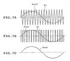
- the PWM circuit 65 includes a comparator 70 comparing the aforesaid PWM control signal Vsin′ with a carrier wave frequency signal Sc such as a triangular wave of 16 kHz, for example, as shown in FIG. 7A.
- the carrier wave frequency signal Sc is shown as having an excessively low frequency for the purpose of illustration in the drawing. Consequently, the PWM circuit 65 generates drive signals G 1 to G 4 so that a triangular wave high-frequency voltage V 0 (100 V, 50 or 60 Hz) as shown in FIG. 7B is obtained.
- the filter circuit 38 eliminates high frequency components from the voltage V 0 such that AC output V 0 ac of 100 V, 50 or 60 Hz is produced as shown in FIG. 7C.
- the PWM control signal Vsin′ as shown in FIG. 7A denotes the condition where no overcurrent has occurred.
- the microcomputer 61 serves as a power detector, a phase angle detector, a phase detector and a controller. Upon start of operation, the microcomputer 61 controls an output frequency according to the flowchart of FIG. 8. More specifically, at step Q 1 , the microcomputer 61 detects an initial zero cross in one cycle of the sine-wave reference voltage Vsin (see timing t 0 in FIG. 4). Since an effective zero cross of the sine-wave reference signal Vsin corresponds with an effective zero cross of the output voltage V 0 , timing t 0 of the initial zero cross in one cycle of the reference signal Vsin is detected.
- the microcomputer 61 determines which an instantaneous value Is( 1 ) of the current is, positive or negative, namely, whether the current leads or lags behind the voltage, thereby detecting whether a phase angle ⁇ is in the leading or lag phase.
- the microcomputer 61 obtains products of the instantaneous values Is(n) at times ( 1 ) to ( 6 ) in FIG. 4 and the sine-wave reference signal Vsin(n) which is previously found, storing data of the obtained values.
- the microcomputer 61 further obtains a square of the instantaneous value I(n) at step Q 5 , storing data of the obtained value (step Q 5 ).
- step Q 8 The microcomputer 61 advances to step Q 8 to calculate an effective current value I, which is obtained by the equation:
- I (( Is ( 1 ) 2 +( Is ( 2 ) 2 + . . . +( Is ( 6 ) 2 )/6) 1/2 .
- step Q 9 the microcomputer 61 calculates a phase angle ⁇ .
- the relationship between an apparent power (I ⁇ E) and the effective power P is shown by the equation:
- phase angle ⁇ is obtained from cos ⁇ since:
- the microcomputer 61 determines that the phase angle ⁇ is in the leading phase. On the other hand, when the instantaneous value Is(n) is negative at step Q 2 , the microcomputer 61 determines that the phase angle ⁇ is in the lag phase.
- an output frequency is set on the basis of the phase angle ⁇ and the leading or lag phase.
- This setting is executed on the basis of a data table as shown in FIG. 9. More specifically, when the phase angle is in the leading phase, the output frequency is set so as to become small according to the phase angle ⁇ . The output frequency is set so as to become large according to the phase angle ⁇ when the phase angle is in the. lag phase. For example, the output frequency is 50.0 Hz when the phase angle ⁇ is 0°. The output frequency is 50.1 Hz when the phase angle ⁇ is 90°. The output frequency is linearly set between these values.
- the microcomputer 61 has a function of detecting the DC voltage Vdc to adjust the output voltage irrespective of an on-off control of the thyristors 39 to 41 . More specifically, as shown in steps R 1 to R 3 of FIG. 10, when the DC voltage Vdc is at or above 180 V, the output voltage is controlled to be increased. That is, the amplitude of the sine wave reference signal Vsin is increased so that the output voltage is increased. For example, when the DC voltage Vdc rises 1 V from 180 V, the output frequency is increased 0.01 Hz.
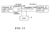
- FIG. 11 Two portable AC power supply units 21 A and 21 B are shown. Assume now that the output frequency of the unit 21 B has instantaneously reduced to 49.96 Hz for some reason (load variation, for example). In this case, a cross current flows from the unit 21 A to the unit 21 B. In the unit 21 B, the current leads the voltage and the phase angle is in the leading phase, whereas the current lags behind the voltage in the unit 21 A such that the phase angle is in the lag phase. In the embodiment, the output frequency is increased when the phase angle is in the lag phase, and the output frequency is reduced when the phase angle is in the leading phase.
- the output frequency is increased in the unit 21 A, whereas the output frequency is reduced in the unit 21 B. Consequently, an amount of cross current flowing into the unit 21 A is reduced such that the cross current is resolved between the units 21 A and 21 B.
- the output frequency since the output frequency is increased or reduced according to the phase angle ⁇ , the output frequency can be controlled promptly so as to take an optimum value.
- the effective power P contains the element of phase angle ⁇ between the output voltage and the output current.
- the effective power P is detected, and the phase angle ⁇ is calculated on the basis of the detected effective power P. Accordingly, an accurate phase angle ⁇ can be detected even when the output current or the signal Is detected by the output current detecting circuit 64 has waveform distortion. Consequently, the accuracy in the detection of the phase angle ⁇ can be improved.
- an appropriate frequency control can be performed on the basis of a phase angle with higher detection accuracy, and the output currents are normally balanced between the power supply units in the case of the parallel operation.
- the effective power is detected in the half cycle of the sine wave reference signal Vsin. Accordingly, the detection of the effective power can be executed in a short period of time and the subsequent frequency control can be carried out quickly. However, the effective power may be detected in one cycle of the sine wave reference signal Vsin, instead.
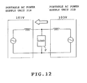
- FIG. 12 illustrates a case where the output voltage of the unit 21 B is higher than the output voltage of the unit 21 A although the output frequencies of both units 21 A and 21 B are the same (50 or 60 Hz).
- a cross current flows from the 21 B to the unit 21 A.
- the output voltage adjusting function of the unit 21 A detects the DC voltage Vdc which is at or above 180 V, thereby increasing the output voltage. As a result, the cross current can be prevented from flowing into the unit 21 A.
- FIGS. 13 and 14 show a second embodiment of the invention.
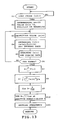
- the second embodiment differs from the first embodiment in that a wattless power is calculated from the effective power so that the output frequency is set according to the leading or lag phase of the phase angle in the wattless power.
- Steps S 1 to S 8 in the flowchart of FIG. 13 are identical with the steps Q 1 to Q 8 in FIG. 8 respectively.
- the value of cos ⁇ is obtained at step S 9 .
- step S 10 the value of sin ⁇ is obtained from cos ⁇ and the wattless power is calculated (wattless power calculator).
- the leading or lag phase of the phase angle is determined at step S 2 (phase detector).
- the phase angle is in the leading phase when the instantaneous value I( 1 ) of the current is positive.
- the phase angle is in the lag phase when the instantaneous value is negative.
- the frequency is set on the basis of the magnitude of the wattless power and the phase with reference to the data table as shown in FIG. 14. For example, when the wattless power in the leading phase is at ⁇ 2800 W (corresponding to phase angle ⁇ of ⁇ 90°), the frequency is set at 49.9 Hz. Consequently, the same effect can be achieved from the second embodiment as from the first embodiment.
- FIGS. 15A to 15 C illustrate a third embodiment of the invention.
- the microcomputer 61 sets a signal Vx having a waveform leading the sine wave reference signal Vsin by 90°.
- the product of the signal Vx and the output current signal Is is obtained six times in a half cycle.
- the six products are added together, whereby the wattless power is detected.
- the wattless power can directly be obtained.
- FIGS. 16A to 16 D illustrate a fourth embodiment of the invention.
- the portable AC power supply units 21 of the first and second embodiments can cope with a case where a relatively small cross current flows into one of the units in parallel operation.
- the phase angle is not more than 90° and the effective power is positive though the phase angle is in the leading or lag phase, as shown in FIG. 16A.
- the cross current is large, switching elements of the inverter circuit of the unit into which the cross current flow may be damaged. Accordingly, the cross current needs to be resolved or eliminated earlier.
- the current signal Is is 90° or more out of phase with the sine wave reference signal Vsin (180° out of phase) and the effective power is negative.
- an output voltage controller is provided for increasing the output voltage when the detected effective power is negative. Consequently, since a large cross current is prevented from flowing into the power supply unit without detection of the phase angle, phase lead or lag, the switching elements of the inverter circuit or the like can effectively be prevented from being damaged.
- an auxiliary controller may be provided for increasing the frequency of the output voltage when the detected effective power is negative. As a result, since the increase in the frequency reduces an amount of the cross current flowing into the power supply unit, the same effect can be achieved from the fourth embodiment as from the first embodiment.
- FIGS. 17 to 21 illustrate a fifth embodiment of the invention.
- the CPU (not shown) of the microcomputer 61 in the first embodiment further severs as a corrected value calculator, a phase angle detector and a sine wave reference data corrector, so that the sine wave reference signal is corrected to prevent variations in the output voltage.
- correction of the sine wave reference signal will now be described with reference to FIG. 17.
- the correction is executed in parallel with the control as shown in FIG. 8.
- the microcomputer 61 delivers the sine wave reference signal Vsin as will be described later.
- the PWM circuit 65 delivers a PWM signal on the basis of the sine wave reference signal Vsin.
- the inverter circuit 37 controls the switching elements 45 to 48 on the basis of the PWM signal thereby to deliver a high-frequency voltage V 0 as shown in FIG. 7.
- the output voltage detecting circuit 63 detects output voltage, and the microcomputer 61 determines whether the output current signal Is is in the leading or lag phase at zero cross t 0 and zero cross t 1 of the output voltage Vs, as shown in FIG.
- the microcomputer 61 determines that the output current signal is in the leading phase.
- the microcomputer 61 determines that the output current signal Is is in the lag phase.
- the microcomputer 61 determines that the output current signal Is is in the leading phase.
- the microcomputer 61 determines that the output current signal Is is in the lag phase.
- the microcomputer 61 corrects the sine wave reference data D(n) according to the flowcharts of FIGS. 17 and 18 thereby to correct the sine wave reference signal Vsin. More specifically, the microcomputer 61 sets the parameter n of the sine wave reference data D(n) at 0 at step Q 1 in FIG. 17. The microcomputer 61 then increments the parameter n at step Q 2 and carries out the correcting control at step Q 3 . The correcting control is shown as a subroutine in FIG. 18. At step R 1 , the microcomputer 61 reads from ROM 61 b the sine wave reference data D(n) corresponding to the current output timing.
- data D( 1 ) and sine wave reference data leading the data D( 1 ) by 900 and displaced by a phase angle 0 since 256 parameters n are present in 360° of electrical angle (one cycle at 50 or 60 Hz), n is increased to “2,” “3,” “4” and so on for every increase of (360/256)° when n is “1” at the phase angle of 0°.
- the aforesaid (360/256)° becomes ( ⁇ fraction (1/50) ⁇ sec.)/256 at 50 Hz and ( ⁇ fraction (1/60) ⁇ sec.)/256 at 60 Hz.
- Sequence “y” leads sequence “x” by the phase angle ⁇ .
- sequence “y” is out of the range between 1 and 256, the data displaced from sequence “y” by 180° is inverted. See “y′” in FIG. 19.
- the sine wave reference data D(n+90°+ ⁇ ) is the sine wave reference data D(y) in this sequence “y”.
- the microcomputer 61 then multiplies the data D(n+90°+ ⁇ ) by a correction value Ih to originate correction data Dh.
- the correction value Ih will be described later.
- the microcomputer 61 then advances to step R 3 where the correction data Dh is added to the current sine wave reference data D(n) to obtain new sine wave reference data D(n). Data stored on RAM 61 c is renewed such that the new data D(n) is stored on RAM 61 c .
- the microcomputer 61 further advances to step Q 4 in FIG. 17 to deliver the new data D(n) to the D/A converter 61 d .
- An output cycle is set to be at time intervals of 256 for ⁇ fraction (1/50) ⁇ sec. in the frequency of 50 Hz and at time intervals of 256 for ⁇ fraction (1/60) ⁇ sec. in the frequency of 60 Hz.
- step Q 7 the microcomputer 61 squares the detected current value Id(n), storing data of the squared value. The microcomputer 61 then advances to step Q 8 to determine whether n is 128 or 256. Since n is less than 128 at the beginning, the microcomputer 61 determines in the negative (NO) at step Q 8 , returning to step Q 2 . Thus, when steps Q 2 to Q 7 are repeatedly carried out at 128 times or a half cycle is completed, the microcomputer 61 determines in the affirmative at step Q 8 , advancing to step Q 9 where the microcomputer 61 determines whether n is 128. When n is 128, the microcomputer 61 advances to step Q 10 to calculate effective power P when n is 1 to 128. In this case, effective power P is obtained by the equation:
- the microcomputer 61 calculates an effective current value I at step Q 11 .
- the effective current value I is obtained by the equation:
- I (( Id ( 1 ) 2 + . . . Id ( 128 ) 2 )/ 128) 1/2 .
- the microcomputer 61 obtains the phase angle ⁇ at step Q 12 . More specifically, the relationship between an apparent power (I ⁇ E) and the effective power P is shown by the equation:
- phase angle ⁇ is obtained from cos ⁇ since:
- the result of detection at step S 2 in FIG. 21 is the latest.
- the phase angle ⁇ is in the leading phase when the latest result of detection is positive.
- the phase angle ⁇ is in the lagging phase when the result of detection is negative.
- a correction value Ih is calculated at step Q 13 .
- the correction value is obtained by multiplying a factor k by an effective value I of current.
- the factor k depends upon the reactor 55 of the filter circuit 38 etc.
- the microcomputer 61 reads out the sine wave reference data D(n) corresponding to the current output timing.
- the microcomputer 61 further reads out the sine wave reference data D(y) leading the read data D(n) by 90° and shifted by the phase angle ⁇ relative to the read data D(n).
- the microcomputer 61 multiplies the correction value Ih by the read sine wave reference data D(y) to obtain correction data Dh.
- the microcomputer 61 further adds the correction data Dh to the sine wave reference data D(n) corresponding to the current output timing to obtain new sine wave reference data D(n).
- the corrected sine wave reference data D(n) is delivered to the D/A converter 61 d , which delivers the sine wave reference signal corrected on the basis of the corrected sine wave reference data D(n). Consequently, the variations in the output voltage can be reduced. Further, the above-described arrangement requires no analog circuit such as a differential amplifier including resistors and capacitors or a power factor correcting circuit including resistors, capacitors and an operational amplifier. Consequently, the circuit arrangement can be simplified and accordingly, the cost can be reduced.
- the current value Id is detected in the half cycle of the output voltage signal Vs corresponding to the half cycle of the output voltage, and the effective current value I is calculated. Consequently, the output current value can be detected in a short period of time, and the detected effective value I contains a reduced amount of error detection.
- the current value Id may be detected in one cycle of the output voltage signal Vs, instead.
- the effective power P is calculated on the basis of the sine wave reference data D(n) in the half cycle and the effective value I, and the phase angle ⁇ is calculated on the basis of the effective power P in the half cycle. Consequently, the phase angle can be detected in a short period of time.
- the effective power P may be calculated on the basis of the data D(n) detected in one cycle.
- each of calculation of the correction value Ih and detection of the phase angle ⁇ may be carried out in a half cycle of the output voltage signal Vs.
- the obtained correction value Ih and phase angle ⁇ are used for correction of the data D(n) and output of the signal Vsin in the next half cycle. Consequently, the control for correction of the sine wave reference signal Vsin can be performed quickly such that a quick feedback control can be realized.
- the sine wave reference data D(n) corresponding to 256 phase angles in one cycle of the AC voltage to be delivered are stored in the foregoing embodiments.
- the number of data should not be limited to 256.
- the data in a half cycle of the AC voltage may be stored, instead. In this case, since the polarity in a first half cycle is inverted in the next half cycle, the data used in the first half cycle needs to be inverted in the next half cycle.
Landscapes
- Engineering & Computer Science (AREA)
- Power Engineering (AREA)
- Inverter Devices (AREA)
- Ac-Ac Conversion (AREA)
Abstract
Description
- 1. Field of the Invention
- This invention relates to an inverter suitable for use with portable AC power supply units.
- 2. Description of the Related Art
- Inverters have been incorporated in portable AC power supply units, drivers of AC motors, uninterruptable power supply units, etc. As one of modes of application, a plurality of, for example, two portable AC power supply units are connected in parallel with each other to drive a load. In this case, the portable AC power supply units are operated with output frequencies in synchronism with each other. Current (cross current) flows from one of the power supply units to the other when a change in the load etc. results in a subtle change in the frequency of either power supply unit. The cross current sometimes breaks circuit components of the portable AC power supply unit. The cross current flows from the power supply unit with a higher output frequency to the one with a lower output frequency.
- As one of measures preventing the cross current flowing between the portable AC power supply units, a lag or lead in a phase between output voltage and output current is monitored. An output frequency is adjusted on the basis of the phase lag or lead, whereby the cross current is prevented. FIG. 22 shows one of the conventional arrangements for preventing the cross current. A portable AC
power supply unit 1 comprises an enginedrive AC generator 2 and aninverter unit 3 havingoutput terminals 3 a and 3 b from which a sinusoidal AC voltage is delivered. Theinverter unit 3 includes arectifier circuit 4 rectifying a three-phase AC voltage generated by theAC generator 2, asmoothing capacitor 5, a single-phase full-bridge inverter circuit 6, afilter circuit 7, acontrol circuit 8 and adrive circuit 9. Thecontrol circuit 8 includes amicrocomputer 10 and a pulse-width-modulation (PWM)circuit 11 generating a drive signal. Theinverter circuit 6 is adapted to be connected to a load. When a plurality of the portable ACpower supply units 1 are to be connected to each other, theinverter circuits 6 of the respectivepower supply units 1 are connected to each other. - In the above-described arrangement, the
control circuit 8 controls thegenerator 2 so that the engine maintains a predetermined number of revolution. Thecontrol circuit 8 further performs a PWM control so that a sine wave AC voltage having a predetermined voltage (for example, an effective value of 100V) at a predetermined frequency (50 Hz or 60 Hz) is delivered from theoutput terminals 3 a and 3 b. Thecontrol circuit 8 further includes an outputvoltage detecting circuit 12 detecting an output voltage of theinverter circuit 6, an outputcurrent detecting circuit 13 detecting an output current of theinverter circuit 6 and a phasedifference detecting circuit 14 detecting a phase difference between the output voltage and the output current. Thecontrol circuit 8 increases an output frequency when the output current lags behind the output voltage. Further, thecontrol circuit 8 decreases the output frequency when the output current leads the output voltage. Consequently, an output balance is achieved between the two ACpower supply units 1 connected in parallel with each other. The output frequencies are adjusted in a range between 49.90 Hz and 50.10 Hz when the portable AC power supply units are of 50 Hz specification. - In the above-mentioned detection of the phase difference, the phase difference is detected by measuring a time from a zero cross point of the output voltage (AC) to a zero cross point of the output current. However, when a detected waveform of the output current is distorted, the zero crossing may occur twice or the timing of the zero crossing may not be normal. As a result, the output currents are not balanced between the power supply units in a parallel operation of the power supply units.
- Therefore, an object of the present invention is to provide an inverter in which the output currents are balanced in the parallel operation of the power supply units.
- The present invention provides an inverter comprising a DC power supply circuit, an inverter circuit having a plurality of switching elements and switching an output of the DC power supply circuit on the basis of a PWM signal to deliver a high-frequency voltage, a filter circuit converting the high-frequency voltage to a substantially sinusoidal AC voltage, a power detector detecting an effective or wattless power of the AC power, a phase angle calculator calculating a phase angle of current relative to voltage from the detected effective or wattless power, a phase. detector detecting a leading or lagging state of the phase angle, and a controller decreasing a frequency of the output voltage when the phase detector detects the leading state of the phase angle, the controller increasing the frequency of the output voltage when the phase detector detects the lagging state of the phase angle.
- According to the above-described arrangement, the effective power or wattless power contains a phase angle element between the output voltage and the output current. The effective or wattless power is detected, and the phase angle calculator calculates a phase angle on the basis of the detected effective or wattless power. Consequently, an accurate phase angle can be detected even when the output current or the output current detector contains a waveform distortion and accordingly, the accuracy in the detection of the phase angle can be improved. Furthermore, the phase detector detects the leading or lagging state of the calculated phase angle, and the controller decreases the frequency of the output voltage when the phase detector detects the leading state of the phase angle. The phase detector increases the frequency of the output voltage when the phase detector detects the lagging state of the phase angle. Consequently, an accurate frequency control can be carried out, and the output currents are balanced in the parallel operation of the power supply units.
- Other objects, features and advantages of the present invention will become clear upon reviewing the following description of a preferred embodiment, made with reference to the accompanying drawings, in which:
- FIG. 1 is a circuit diagram showing an electrical arrangement of a portable AC power supply unit to which an inverter of an embodiment in accordance with the present invention is applied;
- FIG. 2 is a schematic block diagram showing functions of a microcomputer employed in the power supply unit;
- FIG. 3 is a graph showing a data table of sine wave reference data;
- FIG. 4 is a graph showing a sine wave reference signal and an output current detection signal;
- FIG. 5 is a circuit diagram showing a part of a PWM circuit;
- FIGS. 6A to 6C show waveforms at points in the circuit of FIG. 5 respectively;
- FIGS. 7A to 7C shows waveforms related to the PWM control;
- FIG. 8 is a flowchart showing a control manner by the microcomputer;
- FIG. 9 shows frequency setting data;
- FIG. 10 is a flowchart showing another control manner by the microcomputer;
- FIG. 11 shows a parallel operation of two portable AC power supply units with cross current due to output frequency occurring;
- FIG. 12 shows a parallel operation of two portable AC power supply units with cross current due to output voltage occurring;
- FIG. 13 is a flowchart showing a control manner in a second embodiment in accordance with the invention;
- FIG. 14 is a view similar to FIG. 9;
- FIGS. 15A to 15C are waveform charts showing a third embodiment in accordance with the invention;
- FIGS. 16A to 16D are waveform charts showing a fourth embodiment in accordance with the invention;
- FIG. 17 is a flowchart showing an overall control manner for correction in a fifth embodiment in accordance with the invention;
- FIG. 18 is a flowchart showing a control manner for correction;
- FIG. 19 is a flowchart showing a control manner for correction using sine wave reference data;
- FIG. 20 is a waveform chart showing an output voltage signal and an output current signal;
- FIG. 21 is a flowchart showing determination of a leading or lagging state of the output current; and
- FIG. 22 is a view similar to FIG. 1, showing a conventional power supply unit.
- An embodiment in accordance with the present invention will be described with reference to FIGS. 1 to 12. The inverter of the invention is incorporated in a portable AC power supply unit in the embodiment. Referring to FIG. 1, an electrical arrangement of the portable AC
power supply unit 21 generating AC power of 100 V and 50 Hz or 60 Hz, for example. The portable ACpower supply unit 21 comprises a three-phase AC generator 22 driven by an engine (not shown) and a single-phase inverter unit 23 connected to a rear stage of the generator. Thegenerator 22 includes a rotor, an armature neither of which is shown, and a steppingmotor 24 controlling a flow rate of fuel (gasoline) to the engine so that a rotational speed of the engine is controlled. The armature has Y-connectedprimary windings terminals terminals 28 a and 28 b are connected to inputterminals inverter unit 23 respectively. - The
inverter unit 23 will be described in detail. Arectifier circuit 33 is connected between DCpower supply lines rectifier circuit 33 is further connected to theinput terminals capacitor 34 and aninverter circuit 37 are also connected between the DCpower supply lines inverter circuit 37 is further connected tooutput terminals inverter unit 23. Afilter circuit 38 is connected to theinverter circuit 37. Therectifier circuit 33 serves as a DC power supply circuit in the invention. Therectifier circuit 33 comprisesthyristors 39 to 41 anddiodes 42 to 44 connected into a three-phase hybrid bridge configuration. Theinverter circuit 37 comprises transistors (switching elements) 45 to 48 anddiodes 49 to 52 connected into a full bridge configuration. - The
filter circuit 38 comprises areactor 55 and acapacitor 56. Thereactor 55 is interposed between theoutput terminal 53 of theinverter circuit 37 and theoutput terminal 35 of theinverter unit 23. Thecapacitor 56 is connected between theoutput terminals inverter unit 23. Theinverter circuit 37 has anoutput terminal 54 directly connected to theoutput terminal 36 of theinverter unit 23. Acurrent transformer 57 is connected across a current path between theoutput terminal 54 and thefilter circuit 38 for detecting an output current. In a parallel operation of a plurality of the ACpower supply units 21, theoutput terminals inverter units 23 are connected in parallel with each other or one another, respectively. - The
inverter unit 23 further comprises a controlpower supply circuit 58, acontrol circuit 59 and adrive circuit 60. AC voltage induced in the auxiliary winding 26 is supplied to inputterminals 30 a and 30 b of the controlpower supply circuit 58. The supplied AC voltage is rectified and smoothed into a control DC voltage (5 V or ±15 V, for example) for energizing thecontrol circuit 59. The AC voltage induced in the auxiliary winding 26 is also supplied to thecontrol circuit 59 for detection of the rotational speed of the engine. Thecontrol circuit 59 comprises amicrocomputer 61, a DCvoltage detecting circuit 62, an outputvoltage detecting circuit 63, an output current detectingcircuit 64 and a pulse width modulation (PWM)circuit 65. Themicrocomputer 61 comprises aCPU 61 a, aROM 61 b and aRAM 61 c the latter two of which serve as storage means, and a D/A converter 61 d serving as sine wave reference signal generator, as shown in FIG. 2. Themicrocomputer 61 further includes an input/output port, an A/D converter, a timer circuit, an oscillator circuit none of which are shown. These components are incorporated into a one-chip IC. - The
ROM 61 b stores as initial data sine wave reference data D(n) for one cycle where n changes from 1 to 256. FIG. 3 shows a data table of the sine wave reference data. More specifically, an axis of abscissas denotes a memory address sequence, whereas an axis of ordinates denotes sine wave reference data D(n). The sine wave reference data D(n) is sequentially increased or decreased between 1 and 256. TheRAM 61 c stores new sine wave reference data D(n). The sine wave reference data D(n) stored on theROM 61 b includes 256 data for one cycle as shown in FIG. 3. The 256 data correspond to values of amplitude of a sine wave reference signal Vsin (as shown in FIG. 4). When the power supply frequency is at 50 Hz, the 256 data are sequentially read out by theCPU 61 a at an equal time interval for {fraction (1/50)} sec. When the power supply frequency is at 60 Hz, the 256 data are sequentially read out by theCPU 61 a at an equal time interval for {fraction (1/60)} sec. - The DC
voltage detecting circuit 62 detects DC voltage Vdc between the DCpower supply lines microcomputer 61. Themicrocomputer 61 inputs the DC voltage signal. Themicrocomputer 61 turns off thethyristors 39 to 41 when the input DC voltage Vdc is above 180 V. Themicrocomputer 61 turns on thethyristors 39 to 41 when the input DC voltage Vdc is at or below 180 V. The outputvoltage detecting circuit 63 serving as output current detector includes a voltage divider circuit dividing voltage between theterminals inverter circuit 37 and a filter eliminating carrier wave components from divided rectangular wave voltage, neither of which is shown. The outputvoltage detecting circuit 63 delivers an output voltage signal Vs to themicrocomputer 61 and thePWM circuit 65. The output current detectingcircuit 64 converts the output current detected by thecurrent transformer 57 to a predetermined voltage level. The output current detectingcircuit 64 delivers an output current signal Is as an output current signal to themicrocomputer 61 and thePWM circuit 65. ThePWM circuit 65 executes a PWM control to generate drive signals G1 to G4 for thetransistors 45 to 48 respectively. The drive signals G1 to G4 are applied via thedrive circuits 60 to the bases of thetransistors 45 to 48 respectively. - An output frequency of the
microcomputer 61 is set at either 50 Hz or 60 Hz by an input from an switch input section (not shown). For example, when an AC power supply of 50 Hz (100 V) is to be produced, thePWM circuit 65 is supplied with the sine wave reference signal Vsin as an AC reference voltage having a frequency equal to the set output frequency. The sine wave reference signal Vsin is supplied to anerror amplifier circuit 66 of thePWM circuit 65 as shown in FIG. 5. Theerror amplifier circuit 66 is also supplied with an output voltage signal Vs delivered by the outputvoltage detecting circuit 63. Theerror amplifier circuit 63 executes amplification by subtraction to deliver a PWM control signal Vsin′, whereupon the output voltage signal Vs is adjusted so that voltage and frequency of the signal Vs correspond to set values respectively, namely, a feedback control is carried out for the output voltage. The sine wave reference signal Vsin is also used for calculation of an effective power as will be described later. - The
PWM circuit 65 includes apeak limiter circuit 67 as shown in FIG. 5. Thepeak limiter circuit 67 comprises anoperational amplifier 68 and anintegration circuit 69. The output current signal Is delivered by the output current detectingcircuit 64 is supplied to theoperational amplifier 68. A peak current reference signal Ik is also supplied to theoperational amplifier 68. When the output current signal Is corresponds to an overcurrent, theoperational amplifier 68 is turned on with respect to a portion where the peak current reference signal Ik is exceeded. The aforesaid peak current reference signal Ik includes signal levels of +Ik and −Ik due to hysteresis as shown in FIG. 6A. Since theintegration circuit 69 applies feedback to theoperational amplifier 68, a peak portion of the PWM control signal Vsin′ is cut off substantially into a flat portion as shown in FIG. 6C. Without theintegration circuit 69, the PWM control signal Vsin′ delivered by thepeak limiter circuit 69 would instantaneously rise up and fall down such that the circuit would oscillate. In the embodiment, however, such a problem can be solved since the PWM control signal Vsin′ takes a sinusoidal waveform when no overcurrent occurs, as shown by broken line in FIG. 6C. - The
PWM circuit 65 includes acomparator 70 comparing the aforesaid PWM control signal Vsin′ with a carrier wave frequency signal Sc such as a triangular wave of 16 kHz, for example, as shown in FIG. 7A. The carrier wave frequency signal Sc is shown as having an excessively low frequency for the purpose of illustration in the drawing. Consequently, thePWM circuit 65 generates drive signals G1 to G4 so that a triangular wave high-frequency voltage V0 (100 V, 50 or 60 Hz) as shown in FIG. 7B is obtained. Thefilter circuit 38 eliminates high frequency components from the voltage V0 such that AC output V0 ac of 100 V, 50 or 60 Hz is produced as shown in FIG. 7C. The PWM control signal Vsin′ as shown in FIG. 7A denotes the condition where no overcurrent has occurred. - The
microcomputer 61 serves as a power detector, a phase angle detector, a phase detector and a controller. Upon start of operation, themicrocomputer 61 controls an output frequency according to the flowchart of FIG. 8. More specifically, at step Q1, themicrocomputer 61 detects an initial zero cross in one cycle of the sine-wave reference voltage Vsin (see timing t0 in FIG. 4). Since an effective zero cross of the sine-wave reference signal Vsin corresponds with an effective zero cross of the output voltage V0, timing t0 of the initial zero cross in one cycle of the reference signal Vsin is detected. At step Q2, themicrocomputer 61 determines which an instantaneous value Is(1) of the current is, positive or negative, namely, whether the current leads or lags behind the voltage, thereby detecting whether a phase angle θ is in the leading or lag phase. - Thereafter, the instantaneous value Is(n) where n changes from 1 to 6 is detected from the output current signal Is six times in a half cycle at equal time intervals at step Q 3. An effective instantaneous power P(n) is calculated at step Q4. More specifically, the
microcomputer 61 obtains products of the instantaneous values Is(n) at times (1) to (6) in FIG. 4 and the sine-wave reference signal Vsin(n) which is previously found, storing data of the obtained values. Themicrocomputer 61 further obtains a square of the instantaneous value I(n) at step Q5, storing data of the obtained value (step Q5). When steps Q3 to Q5 have been repeated six times (YES at step Q6), themicrocomputer 61 advances to step Q7 to calculate an effective power P, which is obtained by the equation: - P=P(1)+P(2)+ . . . +P (6).
- The
microcomputer 61 advances to step Q8 to calculate an effective current value I, which is obtained by the equation: - I=((Is(1)2+(Is(2)2+ . . . +(Is(6)2)/6)1/2.
- At step Q 9, the
microcomputer 61 calculates a phase angle θ. The relationship between an apparent power (I×E) and the effective power P is shown by the equation: - P=(I×E)cos θ.
- Accordingly, the phase angle θ is obtained from cos θ since:
- Cos θ=P/(I×E).
- When the instantaneous value Is(n) is positive at step Q 2, the
microcomputer 61 determines that the phase angle θ is in the leading phase. On the other hand, when the instantaneous value Is(n) is negative at step Q2, themicrocomputer 61 determines that the phase angle θ is in the lag phase. - At step Q 10, an output frequency is set on the basis of the phase angle θ and the leading or lag phase. This setting is executed on the basis of a data table as shown in FIG. 9. More specifically, when the phase angle is in the leading phase, the output frequency is set so as to become small according to the phase angle θ. The output frequency is set so as to become large according to the phase angle θ when the phase angle is in the. lag phase. For example, the output frequency is 50.0 Hz when the phase angle θ is 0°. The output frequency is 50.1 Hz when the phase angle θ is 90°. The output frequency is linearly set between these values.
- The
microcomputer 61 has a function of detecting the DC voltage Vdc to adjust the output voltage irrespective of an on-off control of thethyristors 39 to 41. More specifically, as shown in steps R1 to R3 of FIG. 10, when the DC voltage Vdc is at or above 180 V, the output voltage is controlled to be increased. That is, the amplitude of the sine wave reference signal Vsin is increased so that the output voltage is increased. For example, when the DC voltage Vdc rises 1 V from 180 V, the output frequency is increased 0.01 Hz. - Parallel connection of the portable AC
power supply units 21 will now be described. Referring to FIG. 11, two portable ACpower supply units unit 21B has instantaneously reduced to 49.96 Hz for some reason (load variation, for example). In this case, a cross current flows from theunit 21A to theunit 21B. In theunit 21B, the current leads the voltage and the phase angle is in the leading phase, whereas the current lags behind the voltage in theunit 21A such that the phase angle is in the lag phase. In the embodiment, the output frequency is increased when the phase angle is in the lag phase, and the output frequency is reduced when the phase angle is in the leading phase. Accordingly, the output frequency is increased in theunit 21A, whereas the output frequency is reduced in theunit 21B. Consequently, an amount of cross current flowing into theunit 21A is reduced such that the cross current is resolved between theunits - In the foregoing embodiment, the effective power P contains the element of phase angle θ between the output voltage and the output current. The effective power P is detected, and the phase angle θ is calculated on the basis of the detected effective power P. Accordingly, an accurate phase angle θ can be detected even when the output current or the signal Is detected by the output current detecting
circuit 64 has waveform distortion. Consequently, the accuracy in the detection of the phase angle θ can be improved. Thus, in the frequency control of the output voltage, an appropriate frequency control can be performed on the basis of a phase angle with higher detection accuracy, and the output currents are normally balanced between the power supply units in the case of the parallel operation. - Particularly, the effective power is detected in the half cycle of the sine wave reference signal Vsin. Accordingly, the detection of the effective power can be executed in a short period of time and the subsequent frequency control can be carried out quickly. However, the effective power may be detected in one cycle of the sine wave reference signal Vsin, instead.
- FIG. 12 illustrates a case where the output voltage of the
unit 21B is higher than the output voltage of theunit 21A although the output frequencies of bothunits unit 21A. The output voltage adjusting function of theunit 21A detects the DC voltage Vdc which is at or above 180 V, thereby increasing the output voltage. As a result, the cross current can be prevented from flowing into theunit 21A. - FIGS. 13 and 14 show a second embodiment of the invention. The second embodiment differs from the first embodiment in that a wattless power is calculated from the effective power so that the output frequency is set according to the leading or lag phase of the phase angle in the wattless power. Steps S 1 to S8 in the flowchart of FIG. 13 are identical with the steps Q1 to Q8 in FIG. 8 respectively. The value of cos θ is obtained at step S9. At step S10, the value of sin θ is obtained from cos θ and the wattless power is calculated (wattless power calculator). The leading or lag phase of the phase angle is determined at step S2 (phase detector). The phase angle is in the leading phase when the instantaneous value I(1) of the current is positive. The phase angle is in the lag phase when the instantaneous value is negative. At step S11, the frequency is set on the basis of the magnitude of the wattless power and the phase with reference to the data table as shown in FIG. 14. For example, when the wattless power in the leading phase is at −2800 W (corresponding to phase angle θ of −90°), the frequency is set at 49.9 Hz. Consequently, the same effect can be achieved from the second embodiment as from the first embodiment.
- FIGS. 15A to 15C illustrate a third embodiment of the invention. As another manner of detecting the wattless power, the
microcomputer 61 sets a signal Vx having a waveform leading the sine wave reference signal Vsin by 90°. The product of the signal Vx and the output current signal Is is obtained six times in a half cycle. The six products are added together, whereby the wattless power is detected. Thus, the wattless power can directly be obtained. - FIGS. 16A to 16D illustrate a fourth embodiment of the invention. The portable AC
power supply units 21 of the first and second embodiments can cope with a case where a relatively small cross current flows into one of the units in parallel operation. When the cross current is small, the phase angle is not more than 90° and the effective power is positive though the phase angle is in the leading or lag phase, as shown in FIG. 16A. However, when the cross current is large, switching elements of the inverter circuit of the unit into which the cross current flow may be damaged. Accordingly, the cross current needs to be resolved or eliminated earlier. In this case, the current signal Is is 90° or more out of phase with the sine wave reference signal Vsin (180° out of phase) and the effective power is negative. - In view of the above-described problem, an output voltage controller is provided for increasing the output voltage when the detected effective power is negative. Consequently, since a large cross current is prevented from flowing into the power supply unit without detection of the phase angle, phase lead or lag, the switching elements of the inverter circuit or the like can effectively be prevented from being damaged. In this case, an auxiliary controller may be provided for increasing the frequency of the output voltage when the detected effective power is negative. As a result, since the increase in the frequency reduces an amount of the cross current flowing into the power supply unit, the same effect can be achieved from the fourth embodiment as from the first embodiment.
- FIGS. 17 to 21 illustrate a fifth embodiment of the invention. In the fifth embodiment, the CPU (not shown) of the
microcomputer 61 in the first embodiment further severs as a corrected value calculator, a phase angle detector and a sine wave reference data corrector, so that the sine wave reference signal is corrected to prevent variations in the output voltage. - Correction of the sine wave reference signal will now be described with reference to FIG. 17. The correction is executed in parallel with the control as shown in FIG. 8. Upon start of the operation, the
microcomputer 61 delivers the sine wave reference signal Vsin as will be described later. ThePWM circuit 65 delivers a PWM signal on the basis of the sine wave reference signal Vsin. Theinverter circuit 37 controls the switchingelements 45 to 48 on the basis of the PWM signal thereby to deliver a high-frequency voltage V0 as shown in FIG. 7. At this time, the outputvoltage detecting circuit 63 detects output voltage, and themicrocomputer 61 determines whether the output current signal Is is in the leading or lag phase at zero cross t0 and zero cross t1 of the output voltage Vs, as shown in FIG. 20. More specifically, when detecting the zero cross t0 (from the negative to the positive) of the output voltage signal Vs at step S1 in FIG. 21 and detecting a positive digital value Id of the output current signal Is at step S2, themicrocomputer 61 determines that the output current signal is in the leading phase. On the other hand, when the digital value Id of the output current signal Is is negative, themicrocomputer 61 determines that the output current signal Is is in the lag phase. When detecting the zero cross t1 (from the positive to the negative) of the output voltage signal Vs at step S3 and detecting a negative digital value Id of the output current signal Is at step S4, themicrocomputer 61 determines that the output current signal Is is in the leading phase. When the digital value Id is positive, themicrocomputer 61 determines that the output current signal Is is in the lag phase. FIG. 20 shows a case where the detected current Is lags behind the detected voltage Vs. - At this time, the
microcomputer 61 corrects the sine wave reference data D(n) according to the flowcharts of FIGS. 17 and 18 thereby to correct the sine wave reference signal Vsin. More specifically, themicrocomputer 61 sets the parameter n of the sine wave reference data D(n) at 0 at step Q1 in FIG. 17. Themicrocomputer 61 then increments the parameter n at step Q2 and carries out the correcting control at step Q3. The correcting control is shown as a subroutine in FIG. 18. At step R1, themicrocomputer 61 reads fromROM 61 b the sine wave reference data D(n) corresponding to the current output timing. In this case, data D(1) and sine wave reference data leading the data D(1) by 900 and displaced by aphase angle 0. For example, since 256 parameters n are present in 360° of electrical angle (one cycle at 50 or 60 Hz), n is increased to “2,” “3,” “4” and so on for every increase of (360/256)° when n is “1” at the phase angle of 0°. When converted to time, the aforesaid (360/256)° becomes ({fraction (1/50)} sec.)/256 at 50 Hz and ({fraction (1/60)} sec.)/256 at 60 Hz. - For example, when the phase angle θ is 30° and in the leading phase, the parameter n (n=na) becomes sequence “x” which leads na by 90° as shown in FIG. 19. Sequence “y” leads sequence “x” by the phase angle θ. When sequence “y” is out of the range between 1 and 256, the data displaced from sequence “y” by 180° is inverted. See “y′” in FIG. 19. The sine wave reference data D(n+90°+θ) is the sine wave reference data D(y) in this sequence “y”. At step R 2, the
microcomputer 61 then multiplies the data D(n+90°+θ) by a correction value Ih to originate correction data Dh. The correction value Ih will be described later. Themicrocomputer 61 then advances to step R3 where the correction data Dh is added to the current sine wave reference data D(n) to obtain new sine wave reference data D(n). Data stored onRAM 61 c is renewed such that the new data D(n) is stored onRAM 61 c. Themicrocomputer 61 further advances to step Q4 in FIG. 17 to deliver the new data D(n) to the D/A converter 61 d. An output cycle is set to be at time intervals of 256 for {fraction (1/50)} sec. in the frequency of 50 Hz and at time intervals of 256 for {fraction (1/60)} sec. in the frequency of 60 Hz. - At step Q 7, the
microcomputer 61 squares the detected current value Id(n), storing data of the squared value. Themicrocomputer 61 then advances to step Q8 to determine whether n is 128 or 256. Since n is less than 128 at the beginning, themicrocomputer 61 determines in the negative (NO) at step Q8, returning to step Q2. Thus, when steps Q2 to Q7 are repeatedly carried out at 128 times or a half cycle is completed, themicrocomputer 61 determines in the affirmative at step Q8, advancing to step Q9 where themicrocomputer 61 determines whether n is 128. When n is 128, themicrocomputer 61 advances to step Q10 to calculate effective power P when n is 1 to 128. In this case, effective power P is obtained by the equation: - P=P(1)+P(2)+ . . . +P(128).
- The
microcomputer 61 calculates an effective current value I at step Q11. The effective current value I is obtained by the equation: - I=((Id(1)2 + . . . Id(128)2)/128) 1/2.
- Then, the
microcomputer 61 obtains the phase angle θ at step Q12. More specifically, the relationship between an apparent power (I×E) and the effective power P is shown by the equation: - P=(I×E)cos θ.
- Accordingly, the phase angle θ is obtained from cos θ since:
- Cos θ=P/(I×E).
- In an initial half cycle, the result of detection at step S 2 in FIG. 21 is the latest. The phase angle θ is in the leading phase when the latest result of detection is positive. On the other hand, the phase angle θ is in the lagging phase when the result of detection is negative.
- A correction value Ih is calculated at step Q 13. The correction value is obtained by multiplying a factor k by an effective value I of current. The factor k depends upon the
reactor 55 of thefilter circuit 38 etc. Thereafter, themicrocomputer 61 returns to step Q2 to carry out the same control in a latter half cycle (where n=129 to 256) as described above for the first half cycle. The phase angle θ and the correction value Ih obtained in the first half cycle (where n=1 to 128) are used in the latter half cycle. When the control at steps Q2 through Q7 is executed at 256 times, themicrocomputer 61 determines in the affirmative at step Q8 and in the negative at step Q9, executing steps Q14 to Q17 which are substantially identical with respective steps Q10 to Q13 with the exception of n=129 to 256. Themicrocomputer 61 then returns to step Q1. Thus, the sine wave reference data D(n) for one cycle is supplied to the D/A converter 61 d. The D/A converter 61 d delivers the sine wave reference signal Vsin on the basis of the supplied data D(n). The delivered sine wave reference signal Vsin is supplied to thePWM circuit 65. - According to the above-described embodiment, the
microcomputer 61 reads out the sine wave reference data D(n) corresponding to the current output timing. Themicrocomputer 61 further reads out the sine wave reference data D(y) leading the read data D(n) by 90° and shifted by the phase angle θ relative to the read data D(n). Themicrocomputer 61 multiplies the correction value Ih by the read sine wave reference data D(y) to obtain correction data Dh. Themicrocomputer 61 further adds the correction data Dh to the sine wave reference data D(n) corresponding to the current output timing to obtain new sine wave reference data D(n). Thus, data correction is performed in consideration of the lag of 90° due to thefilter circuit 38, the phase angle θ of the output current due to the load and an L component peculiar to thefilter circuit 38. The corrected sine wave reference data D(n) is delivered to the D/A converter 61 d, which delivers the sine wave reference signal corrected on the basis of the corrected sine wave reference data D(n). Consequently, the variations in the output voltage can be reduced. Further, the above-described arrangement requires no analog circuit such as a differential amplifier including resistors and capacitors or a power factor correcting circuit including resistors, capacitors and an operational amplifier. Consequently, the circuit arrangement can be simplified and accordingly, the cost can be reduced. - The current value Id is detected in the half cycle of the output voltage signal Vs corresponding to the half cycle of the output voltage, and the effective current value I is calculated. Consequently, the output current value can be detected in a short period of time, and the detected effective value I contains a reduced amount of error detection. On the other hand, the current value Id may be detected in one cycle of the output voltage signal Vs, instead. Further, the effective power P is calculated on the basis of the sine wave reference data D(n) in the half cycle and the effective value I, and the phase angle θ is calculated on the basis of the effective power P in the half cycle. Consequently, the phase angle can be detected in a short period of time. On the other hand, the effective power P may be calculated on the basis of the data D(n) detected in one cycle.
- Further, each of calculation of the correction value Ih and detection of the phase angle θ may be carried out in a half cycle of the output voltage signal Vs. The obtained correction value Ih and phase angle θ are used for correction of the data D(n) and output of the signal Vsin in the next half cycle. Consequently, the control for correction of the sine wave reference signal Vsin can be performed quickly such that a quick feedback control can be realized.
- The sine wave reference data D(n) corresponding to 256 phase angles in one cycle of the AC voltage to be delivered are stored in the foregoing embodiments. The number of data should not be limited to 256. Further, the data in a half cycle of the AC voltage may be stored, instead. In this case, since the polarity in a first half cycle is inverted in the next half cycle, the data used in the first half cycle needs to be inverted in the next half cycle.
- The foregoing description and drawings are merely illustrative of the principles of the present invention and are not to be construed in a limiting sense. Various changes and modifications will become apparent to those of ordinary skill in the art. All such changes and modifications are seen to fall within the scope of the invention as defined by the appended claims.
Claims (11)
Priority Applications (1)
| Application Number | Priority Date | Filing Date | Title |
|---|---|---|---|
| US10/457,722 US6771522B2 (en) | 2000-08-31 | 2003-06-10 | Inverter parallel operation system |
Applications Claiming Priority (6)
| Application Number | Priority Date | Filing Date | Title |
|---|---|---|---|
| JP2000262832A JP4693214B2 (en) | 2000-08-31 | 2000-08-31 | Inverter device |
| JP2000-262832 | 2000-08-31 | ||
| JP2001001497A JP4672149B2 (en) | 2001-01-09 | 2001-01-09 | Inverter device |
| JP2001-1497 | 2001-01-09 | ||
| US09/938,856 US20020024828A1 (en) | 2000-08-31 | 2001-08-27 | Inverter suitable for use with portable AC power supply unit |
| US10/457,722 US6771522B2 (en) | 2000-08-31 | 2003-06-10 | Inverter parallel operation system |
Related Parent Applications (1)
| Application Number | Title | Priority Date | Filing Date |
|---|---|---|---|
| US09/938,856 Continuation US20020024828A1 (en) | 2000-08-31 | 2001-08-27 | Inverter suitable for use with portable AC power supply unit |
Publications (2)
| Publication Number | Publication Date |
|---|---|
| US20030198065A1 true US20030198065A1 (en) | 2003-10-23 |
| US6771522B2 US6771522B2 (en) | 2004-08-03 |
Family
ID=26598924
Family Applications (2)
| Application Number | Title | Priority Date | Filing Date |
|---|---|---|---|
| US09/938,856 Abandoned US20020024828A1 (en) | 2000-08-31 | 2001-08-27 | Inverter suitable for use with portable AC power supply unit |
| US10/457,722 Expired - Fee Related US6771522B2 (en) | 2000-08-31 | 2003-06-10 | Inverter parallel operation system |
Family Applications Before (1)
| Application Number | Title | Priority Date | Filing Date |
|---|---|---|---|
| US09/938,856 Abandoned US20020024828A1 (en) | 2000-08-31 | 2001-08-27 | Inverter suitable for use with portable AC power supply unit |
Country Status (2)
| Country | Link |
|---|---|
| US (2) | US20020024828A1 (en) |
| EP (1) | EP1187305A3 (en) |
Cited By (14)
| Publication number | Priority date | Publication date | Assignee | Title |
|---|---|---|---|---|
| US20030173929A1 (en) * | 2002-03-15 | 2003-09-18 | Akio Takemori | Stepping motor driver |
| US20050057213A1 (en) * | 2003-09-11 | 2005-03-17 | Williams Kevin R. | AC motor control system using parallel integrated sub systems |
| US20060193158A1 (en) * | 2005-02-07 | 2006-08-31 | Mitsuo Fukaya | Inverter type AC generator |
| US20070013332A1 (en) * | 2005-07-18 | 2007-01-18 | Schneider Toshiba Inverter Europe Sas | Device for powering a variable speed drive |
| US20070091653A1 (en) * | 2005-10-26 | 2007-04-26 | David Leggate | Method and apparatus for adjustable voltage/adjustable frequency inverter control |
| WO2008049541A1 (en) * | 2006-10-24 | 2008-05-02 | Repower Systems Ag | Controllable phase-angle converter |
| US20090003022A1 (en) * | 2004-03-30 | 2009-01-01 | Makoto Nunoya | Non-Contact Power Supply System |
| US20100123439A1 (en) * | 2008-11-14 | 2010-05-20 | Remy Technologies, L.L.C. | Alternator Regulator With Variable Rotor Field Frequency |
| US20100270985A1 (en) * | 2009-04-24 | 2010-10-28 | Well Shin Technology Co., Ltd. | Dc-dc converter |
| US20110169442A1 (en) * | 2010-01-13 | 2011-07-14 | Canon Kabushiki Kaisha | Drive apparatus for stepping motor |
| US20130094258A1 (en) * | 2011-10-13 | 2013-04-18 | Rockwell Automation Technologies, Inc. | Active front end power converter with diagnostic and failure prevention using peak detector with decay |
| CN103701334A (en) * | 2013-12-31 | 2014-04-02 | 重庆力华科技有限责任公司 | Internal combustion engine-driven inverting generating set and inverting control method thereof |
| KR101395891B1 (en) * | 2007-11-20 | 2014-05-15 | 엘지전자 주식회사 | Motor controller of air conditioner |
| US8964808B2 (en) | 2007-12-21 | 2015-02-24 | Osram Opto Semiconductors Gmbh | Laser light source and method for producing a laser light source |
Families Citing this family (50)
| Publication number | Priority date | Publication date | Assignee | Title |
|---|---|---|---|---|
| US7042110B2 (en) * | 2003-05-07 | 2006-05-09 | Clipper Windpower Technology, Inc. | Variable speed distributed drive train wind turbine system |
| KR100636749B1 (en) * | 2004-10-15 | 2006-10-19 | 주식회사 현대오토넷 | Vehicle AC Power Supply |
| DE102005042615A1 (en) * | 2005-09-07 | 2007-03-08 | Franz Haimer Maschinenbau Kg | Circuit, shrink fitting and method of regulation |
| DE102006062406A1 (en) * | 2006-12-21 | 2008-06-26 | Prettl, Rolf | Converter circuit for the exchange of electrical power quantities, method for driving a converter circuit and power generator |
| US7852643B2 (en) * | 2007-06-27 | 2010-12-14 | General Electric Company | Cross current control for power converter system |
| US7847433B2 (en) * | 2007-11-27 | 2010-12-07 | Rain Bird Corporation | Universal irrigation controller power supply |
| KR101461559B1 (en) * | 2007-12-21 | 2014-11-13 | 엘지전자 주식회사 | Motor control device of air conditioner |
| US8625315B2 (en) * | 2008-05-09 | 2014-01-07 | Etm Electromatic Inc | Inverter modulator with variable switching frequency |
| JP5809558B2 (en) * | 2008-06-27 | 2015-11-11 | ザ リージェンツ オブ ザ ユニバーシティ オブ カリフォルニア | A circuit for direct energy extraction from charged particle beams. |
| US8493014B2 (en) * | 2009-08-10 | 2013-07-23 | Emerson Climate Technologies, Inc. | Controller and method for estimating, managing, and diagnosing motor parameters |
| US8264192B2 (en) | 2009-08-10 | 2012-09-11 | Emerson Climate Technologies, Inc. | Controller and method for transitioning between control angles |
| US8406021B2 (en) * | 2009-08-10 | 2013-03-26 | Emerson Climate Technologies, Inc. | System and method for reducing line current distortion |
| US8508166B2 (en) | 2009-08-10 | 2013-08-13 | Emerson Climate Technologies, Inc. | Power factor correction with variable bus voltage |
| US8264860B2 (en) * | 2009-08-10 | 2012-09-11 | Emerson Climate Technologies, Inc. | System and method for power factor correction frequency tracking and reference generation |
| US8698433B2 (en) | 2009-08-10 | 2014-04-15 | Emerson Climate Technologies, Inc. | Controller and method for minimizing phase advance current |
| US8344706B2 (en) * | 2009-08-10 | 2013-01-01 | Emerson Climate Technologies, Inc. | System and method for rejecting DC current in power factor correction systems |
| US8476873B2 (en) * | 2009-08-10 | 2013-07-02 | Emerson Climate Technologies, Inc. | System and method for current balancing |
| US8358098B2 (en) * | 2009-08-10 | 2013-01-22 | Emerson Climate Technologies, Inc. | System and method for power factor correction |
| WO2011029480A1 (en) * | 2009-09-11 | 2011-03-17 | Abb Research Ltd | Fault current limitation in dc power transmission systems |
| CN102598455B (en) * | 2009-09-18 | 2017-06-20 | 金斯顿女王大学 | distributed power generation interface |
| CN101895204B (en) * | 2010-06-03 | 2012-05-23 | 山东新风光电子科技发展有限公司 | High voltage converter circuit structure |
| CN103026606B (en) * | 2010-07-28 | 2015-08-05 | 三菱电机株式会社 | Chopper device |
| JP2012078782A (en) * | 2010-09-09 | 2012-04-19 | Ricoh Co Ltd | High voltage power supply device, image forming apparatus, and color image forming apparatus |
| CN103119821B (en) * | 2010-09-30 | 2016-01-13 | Abb研究有限公司 | Multiterminal HVDC system coordination controls |
| CN102162428B (en) * | 2011-02-23 | 2013-12-04 | 深圳市华为安捷信电气有限公司 | Controller, method for controlling energy and detection control signal plate |
| US9634593B2 (en) | 2012-04-26 | 2017-04-25 | Emerson Climate Technologies, Inc. | System and method for permanent magnet motor control |
| CN202634345U (en) * | 2012-05-04 | 2012-12-26 | 中山大洋电机股份有限公司 | An ECM motor controller adaptable to different frequencies and different power supply voltages |
| WO2014026124A1 (en) | 2012-08-10 | 2014-02-13 | Emerson Climate Technologies, Inc. | Motor drive control using pulse-width modulation pulse skipping |
| US9557753B2 (en) * | 2012-10-10 | 2017-01-31 | Maschinefabrik Reinhausen Gmbh | Method for regulating the voltage of a transformer |
| US9939883B2 (en) | 2012-12-27 | 2018-04-10 | Nvidia Corporation | Supply-voltage control for device power management |
| CN203278615U (en) * | 2013-05-22 | 2013-11-06 | Abb技术有限公司 | A power module for a medium-high voltage inverter and an inverter including the same |
| US9766649B2 (en) | 2013-07-22 | 2017-09-19 | Nvidia Corporation | Closed loop dynamic voltage and frequency scaling |
| US9602083B2 (en) | 2013-07-03 | 2017-03-21 | Nvidia Corporation | Clock generation circuit that tracks critical path across process, voltage and temperature variation |
| RU2549917C2 (en) * | 2013-10-04 | 2015-05-10 | Федеральное государственное бюджетное образовательное учреждение высшего профессионального образования "Чувашский государственный университет имени И.Н. Ульянова" | Ultrasonic cleaner of deposits in heat exchangers |
| US10466763B2 (en) * | 2013-12-02 | 2019-11-05 | Nvidia Corporation | Dynamic voltage-frequency scaling to limit power transients |
| EP3262750B1 (en) | 2015-02-25 | 2020-01-29 | Otis Elevator Company | Interposition inductor arrangement for multiple drives in parallel |
| CN105610309B (en) * | 2015-11-18 | 2019-01-18 | 哈尔滨工业大学(威海) | A kind of heavy-duty rectifier using DC side electric current direct injection |
| CN107046370B (en) * | 2016-02-09 | 2020-05-26 | 松下知识产权经营株式会社 | Converter, power transmission system and controller |
| CN107046379B (en) * | 2016-02-09 | 2020-07-10 | 松下知识产权经营株式会社 | Converter, power transmission system and controller |
| EP3343745B1 (en) * | 2016-12-29 | 2020-07-15 | MICROTEC S.r.l. | Inverter-generator apparatus |
| WO2018184076A1 (en) * | 2017-04-07 | 2018-10-11 | Allume Energy Pty Ltd | Behind-the-meter system and method for controlled distribution of solar energy in multi-unit buildings |
| CN107086563B (en) * | 2017-06-15 | 2019-08-23 | 温州大学 | A kind of efficient balance control method of parallel operation system output power |
| CN109981013A (en) * | 2017-12-27 | 2019-07-05 | 上海大郡动力控制技术有限公司 | The discrimination method of electric machine phase current sampling delay time |
| EP3512083B1 (en) * | 2018-01-12 | 2023-08-23 | ABB Schweiz AG | Determining and compensating power transistor switching delay |
| CN110676840A (en) * | 2019-08-30 | 2020-01-10 | 合肥学院 | Power system control equipment and power system control method |
| CN112104252B (en) * | 2020-09-08 | 2021-08-20 | 中车青岛四方车辆研究所有限公司 | Method and device for calculating power of auxiliary converter of motor train unit |
| JP7345673B2 (en) * | 2020-10-26 | 2023-09-15 | 三菱電機株式会社 | Power conversion equipment, motor drive equipment, and refrigeration cycle application equipment |
| US11533013B1 (en) * | 2021-07-29 | 2022-12-20 | Rivian Ip Holdings, Llc | Pulse width modulation clock synchronization |
| US12609541B2 (en) | 2021-09-21 | 2026-04-21 | Volvo Car Corporation | Intelligent battery cell |
| JP7768003B2 (en) * | 2022-03-23 | 2025-11-12 | 株式会社リコー | Power conversion device and image forming device |
Citations (9)
| Publication number | Priority date | Publication date | Assignee | Title |
|---|---|---|---|---|
| US3922594A (en) * | 1974-10-15 | 1975-11-25 | Lorain Prod Corp | Control system for phase displacement regulator circuits |
| US4251736A (en) * | 1979-07-23 | 1981-02-17 | United Technologies Corporation | Method for controlling power flow between an electrochemical cell and a power grid |
| US4639848A (en) * | 1984-05-24 | 1987-01-27 | Kabushiki Kaisha Toshiba | Method and system for controlling an AC-DC converter system |
| US4879639A (en) * | 1987-05-11 | 1989-11-07 | Fuji Electric Co., Ltd. | Power converter for driving an AC motor at a variable speed |
| US5053939A (en) * | 1990-08-27 | 1991-10-01 | Sundstrand Corporation | Control of PWM inverters by pattern development from stored constants relating D.C. link harmonics to output distortion |
| US5083039A (en) * | 1991-02-01 | 1992-01-21 | U.S. Windpower, Inc. | Variable speed wind turbine |
| US5187427A (en) * | 1991-11-27 | 1993-02-16 | U.S. Windpower, Inc. | Static reactive power compensator |
| US5438253A (en) * | 1992-12-07 | 1995-08-01 | Mitsubishi Denki Kabushiki Kaisha | Static var generator using self-commutated inverter |
| US6459601B1 (en) * | 2001-10-18 | 2002-10-01 | Mitsubishi Denki Kabushiki Kaisha | Control circuit of power converter |
Family Cites Families (7)
| Publication number | Priority date | Publication date | Assignee | Title |
|---|---|---|---|---|
| US3675037A (en) * | 1971-06-01 | 1972-07-04 | Bell Telephone Labor Inc | Technique for synchronous parallel operation of static inverters |
| US3864620A (en) * | 1973-09-11 | 1975-02-04 | Westinghouse Electric Corp | Arrangement of parallel static ac power sources proportions |
| JPS61254026A (en) * | 1985-04-30 | 1986-11-11 | 三菱電機株式会社 | Parallel operation control system of ac output converter |
| JP2526992B2 (en) * | 1988-05-30 | 1996-08-21 | 三菱電機株式会社 | AC output converter parallel operation system |
| JP3192498B2 (en) | 1991-11-07 | 2001-07-30 | 本田技研工業株式会社 | Inverter device |
| JP3363170B2 (en) * | 1992-02-10 | 2003-01-08 | 本田技研工業株式会社 | Inverter controlled generator |
| JP3356795B2 (en) | 1992-02-24 | 2002-12-16 | 本田技研工業株式会社 | Generator |
-
2001
- 2001-08-27 US US09/938,856 patent/US20020024828A1/en not_active Abandoned
- 2001-08-30 EP EP01307387A patent/EP1187305A3/en not_active Withdrawn
-
2003
- 2003-06-10 US US10/457,722 patent/US6771522B2/en not_active Expired - Fee Related
Patent Citations (10)
| Publication number | Priority date | Publication date | Assignee | Title |
|---|---|---|---|---|
| US3922594A (en) * | 1974-10-15 | 1975-11-25 | Lorain Prod Corp | Control system for phase displacement regulator circuits |
| US4251736A (en) * | 1979-07-23 | 1981-02-17 | United Technologies Corporation | Method for controlling power flow between an electrochemical cell and a power grid |
| US4639848A (en) * | 1984-05-24 | 1987-01-27 | Kabushiki Kaisha Toshiba | Method and system for controlling an AC-DC converter system |
| US4879639A (en) * | 1987-05-11 | 1989-11-07 | Fuji Electric Co., Ltd. | Power converter for driving an AC motor at a variable speed |
| US5053939A (en) * | 1990-08-27 | 1991-10-01 | Sundstrand Corporation | Control of PWM inverters by pattern development from stored constants relating D.C. link harmonics to output distortion |
| US5083039A (en) * | 1991-02-01 | 1992-01-21 | U.S. Windpower, Inc. | Variable speed wind turbine |
| US5083039B1 (en) * | 1991-02-01 | 1999-11-16 | Zond Energy Systems Inc | Variable speed wind turbine |
| US5187427A (en) * | 1991-11-27 | 1993-02-16 | U.S. Windpower, Inc. | Static reactive power compensator |
| US5438253A (en) * | 1992-12-07 | 1995-08-01 | Mitsubishi Denki Kabushiki Kaisha | Static var generator using self-commutated inverter |
| US6459601B1 (en) * | 2001-10-18 | 2002-10-01 | Mitsubishi Denki Kabushiki Kaisha | Control circuit of power converter |
Cited By (27)
| Publication number | Priority date | Publication date | Assignee | Title |
|---|---|---|---|---|
| US6850026B2 (en) * | 2002-03-15 | 2005-02-01 | Japan Servo Co., Ltd. | Stepping motor driver |
| US20030173929A1 (en) * | 2002-03-15 | 2003-09-18 | Akio Takemori | Stepping motor driver |
| US20050057213A1 (en) * | 2003-09-11 | 2005-03-17 | Williams Kevin R. | AC motor control system using parallel integrated sub systems |
| US6989650B2 (en) * | 2003-09-11 | 2006-01-24 | Oilfield-Electric-Marine, Inc. | AC motor control system using parallel integrated sub systems |
| US20090003022A1 (en) * | 2004-03-30 | 2009-01-01 | Makoto Nunoya | Non-Contact Power Supply System |
| US7733676B2 (en) | 2004-03-30 | 2010-06-08 | Daifuku Co., Ltd. | Non-contact power supply system utilizing synchronized command signals to control and correct phase differences amongst power supply units |
| US20060193158A1 (en) * | 2005-02-07 | 2006-08-31 | Mitsuo Fukaya | Inverter type AC generator |
| US7652900B2 (en) * | 2005-02-07 | 2010-01-26 | Yamaha Motor Power Products Kabushiki Kaisha | Inverter type AC generator with a zero-crossing detection circuit used to provide a synchronized operation and method of operating the same |
| US7336052B2 (en) * | 2005-07-18 | 2008-02-26 | Schneider Toshiba Inverter Europe Sas | Device for powering a variable speed drive |
| US20070013332A1 (en) * | 2005-07-18 | 2007-01-18 | Schneider Toshiba Inverter Europe Sas | Device for powering a variable speed drive |
| US20070091653A1 (en) * | 2005-10-26 | 2007-04-26 | David Leggate | Method and apparatus for adjustable voltage/adjustable frequency inverter control |
| US7626836B2 (en) * | 2005-10-26 | 2009-12-01 | Rockwell Automation Technologies, Inc. | Method and apparatus for adjustable voltage/adjustable frequency inverter control |
| WO2008049541A1 (en) * | 2006-10-24 | 2008-05-02 | Repower Systems Ag | Controllable phase-angle converter |
| US8378514B2 (en) | 2006-10-24 | 2013-02-19 | Repower Systems Ag | Phase-angle offsettng converter to minimize damaging effects of sudden phase changes due to network disturbance |
| KR101395891B1 (en) * | 2007-11-20 | 2014-05-15 | 엘지전자 주식회사 | Motor controller of air conditioner |
| US9559496B2 (en) | 2007-12-21 | 2017-01-31 | Osram Opto Semiconductors Gmbh | Laser light source |
| US9531158B2 (en) | 2007-12-21 | 2016-12-27 | Osram Opto Semiconductors Gmbh | Laser light source |
| US9407063B2 (en) | 2007-12-21 | 2016-08-02 | Osram Opto Semiconductors Gmbh | Laser light source and method for producing a laser light source |
| US8964808B2 (en) | 2007-12-21 | 2015-02-24 | Osram Opto Semiconductors Gmbh | Laser light source and method for producing a laser light source |
| US20100123439A1 (en) * | 2008-11-14 | 2010-05-20 | Remy Technologies, L.L.C. | Alternator Regulator With Variable Rotor Field Frequency |
| US8330430B2 (en) * | 2008-11-14 | 2012-12-11 | Remy Technologies, Llc | Alternator regulator with variable rotor field frequency |
| US20100270985A1 (en) * | 2009-04-24 | 2010-10-28 | Well Shin Technology Co., Ltd. | Dc-dc converter |
| US8508176B2 (en) * | 2010-01-13 | 2013-08-13 | Canon Kabushiki Kaisha | Drive apparatus for stepping motor |
| US20110169442A1 (en) * | 2010-01-13 | 2011-07-14 | Canon Kabushiki Kaisha | Drive apparatus for stepping motor |
| US8902616B2 (en) * | 2011-10-13 | 2014-12-02 | Rockwell Automation Technologies, Inc. | Active front end power converter with diagnostic and failure prevention using peak detector with decay |
| US20130094258A1 (en) * | 2011-10-13 | 2013-04-18 | Rockwell Automation Technologies, Inc. | Active front end power converter with diagnostic and failure prevention using peak detector with decay |
| CN103701334A (en) * | 2013-12-31 | 2014-04-02 | 重庆力华科技有限责任公司 | Internal combustion engine-driven inverting generating set and inverting control method thereof |
Also Published As
| Publication number | Publication date |
|---|---|
| US6771522B2 (en) | 2004-08-03 |
| US20020024828A1 (en) | 2002-02-28 |
| EP1187305A3 (en) | 2006-06-07 |
| EP1187305A2 (en) | 2002-03-13 |
Similar Documents
| Publication | Publication Date | Title |
|---|---|---|
| US6771522B2 (en) | Inverter parallel operation system | |
| US6958589B2 (en) | Inverter controller for driving motor and air conditioner using inverter controller | |
| US4692855A (en) | Constant voltage and frequency type PWM inverter with minimum output distortion | |
| JP2002034160A (en) | Inverter parallel operation device | |
| US20030067793A1 (en) | Pulse with modualtion inverter generation using a correction co-efficient and a reference to the ratio to obtain a real duty ratio | |
| JP4712148B2 (en) | Power converter | |
| EP0769221B1 (en) | Load-commutated synchronous motor drive | |
| JP4693214B2 (en) | Inverter device | |
| JPS58141699A (en) | Motor controller | |
| JP3598936B2 (en) | Inverter generator | |
| JP2001268924A (en) | How to correct the output voltage of a portable generator | |
| JP2001037252A (en) | Method of generating sine-wave for controlling power factor compensation | |
| JP4672149B2 (en) | Inverter device | |
| JP3070314B2 (en) | Inverter output voltage compensation circuit | |
| JP3371522B2 (en) | PWM control voltage source inverter | |
| JP3992652B2 (en) | 3-phase input charger | |
| EP1708351A2 (en) | Control systems for inverters | |
| JPH07108092B2 (en) | AC power supply | |
| JP2968027B2 (en) | Control device for current source inverter | |
| JPH0652998B2 (en) | Method and device for controlling control voltage of three-phase inverter for AC motor power supply | |
| JP3267946B2 (en) | Portable generator | |
| JP3230987B2 (en) | Control device for power converter | |
| JP2001309664A (en) | Inverter device | |
| JP2002051567A (en) | Power converter | |
| JPH1127946A (en) | Pulse width modulation control converter |
Legal Events
| Date | Code | Title | Description |
|---|---|---|---|
| AS | Assignment |
Owner name: KABUSHIKI KAISHA TOSHIBA, JAPAN Free format text: ASSIGNMENT OF ASSIGNORS INTEREST;ASSIGNORS:HAYASHI, HIDETAKE;TAKIMOTO, HITOSHI;YOSHIOKA, TOURU;REEL/FRAME:014175/0025;SIGNING DATES FROM 20011002 TO 20011009 Owner name: SAWAFUJI ELECTRIC CO., LTD., JAPAN Free format text: ASSIGNMENT OF ASSIGNORS INTEREST;ASSIGNORS:HAYASHI, HIDETAKE;TAKIMOTO, HITOSHI;YOSHIOKA, TOURU;REEL/FRAME:014175/0025;SIGNING DATES FROM 20011002 TO 20011009 |
|
| FPAY | Fee payment |
Year of fee payment: 4 |
|
| REMI | Maintenance fee reminder mailed | ||
| FPAY | Fee payment |
Year of fee payment: 8 |
|
| REMI | Maintenance fee reminder mailed | ||
| LAPS | Lapse for failure to pay maintenance fees | ||
| STCH | Information on status: patent discontinuation |
Free format text: PATENT EXPIRED DUE TO NONPAYMENT OF MAINTENANCE FEES UNDER 37 CFR 1.362 |
|
| STCH | Information on status: patent discontinuation |
Free format text: PATENT EXPIRED DUE TO NONPAYMENT OF MAINTENANCE FEES UNDER 37 CFR 1.362 |
|
| FP | Lapsed due to failure to pay maintenance fee |
Effective date: 20160803 |