US20030197981A1 - Spin valve type transducer capable of reducing reproducing gap - Google Patents
Spin valve type transducer capable of reducing reproducing gap Download PDFInfo
- Publication number
- US20030197981A1 US20030197981A1 US10/446,106 US44610603A US2003197981A1 US 20030197981 A1 US20030197981 A1 US 20030197981A1 US 44610603 A US44610603 A US 44610603A US 2003197981 A1 US2003197981 A1 US 2003197981A1
- Authority
- US
- United States
- Prior art keywords
- layer
- magnetic
- set forth
- transducer
- magnetic shield
- Prior art date
- Legal status (The legal status is an assumption and is not a legal conclusion. Google has not performed a legal analysis and makes no representation as to the accuracy of the status listed.)
- Granted
Links
- 230000005291 magnetic effect Effects 0.000 claims abstract description 184
- 239000000758 substrate Substances 0.000 claims description 24
- 238000002955 isolation Methods 0.000 claims description 17
- 229910000859 α-Fe Inorganic materials 0.000 claims description 17
- 239000003302 ferromagnetic material Substances 0.000 claims description 15
- 239000002885 antiferromagnetic material Substances 0.000 claims description 8
- 238000003860 storage Methods 0.000 claims description 6
- 239000011810 insulating material Substances 0.000 claims 5
- 238000000034 method Methods 0.000 description 15
- PNEYBMLMFCGWSK-UHFFFAOYSA-N aluminium oxide Inorganic materials [O-2].[O-2].[O-2].[Al+3].[Al+3] PNEYBMLMFCGWSK-UHFFFAOYSA-N 0.000 description 14
- 230000005294 ferromagnetic effect Effects 0.000 description 9
- 229910001030 Iron–nickel alloy Inorganic materials 0.000 description 8
- 230000005381 magnetic domain Effects 0.000 description 8
- 229910003321 CoFe Inorganic materials 0.000 description 7
- 229910003962 NiZn Inorganic materials 0.000 description 6
- 238000004519 manufacturing process Methods 0.000 description 6
- 229920002120 photoresistant polymer Polymers 0.000 description 6
- 230000007423 decrease Effects 0.000 description 5
- 238000004544 sputter deposition Methods 0.000 description 5
- 239000010931 gold Substances 0.000 description 4
- 238000001659 ion-beam spectroscopy Methods 0.000 description 4
- 230000004048 modification Effects 0.000 description 4
- 238000012986 modification Methods 0.000 description 4
- 229910019041 PtMn Inorganic materials 0.000 description 3
- 229910052593 corundum Inorganic materials 0.000 description 3
- 238000010884 ion-beam technique Methods 0.000 description 3
- 229910001845 yogo sapphire Inorganic materials 0.000 description 3
- 229910019233 CoFeNi Inorganic materials 0.000 description 2
- 229910018979 CoPt Inorganic materials 0.000 description 2
- 230000005303 antiferromagnetism Effects 0.000 description 2
- 230000015572 biosynthetic process Effects 0.000 description 2
- 230000000694 effects Effects 0.000 description 2
- 238000005530 etching Methods 0.000 description 2
- 230000004907 flux Effects 0.000 description 2
- 238000001755 magnetron sputter deposition Methods 0.000 description 2
- 239000002245 particle Substances 0.000 description 2
- 230000035945 sensitivity Effects 0.000 description 2
- BVGSSXDMHDNNIF-UHFFFAOYSA-N (4-oxo-2,3-dihydro-1h-cyclopenta[c]chromen-7-yl) 3-chloro-4-[2-[(2-methylpropan-2-yl)oxycarbonylamino]acetyl]oxybenzoate Chemical compound C1=C(Cl)C(OC(=O)CNC(=O)OC(C)(C)C)=CC=C1C(=O)OC1=CC=C(C2=C(CCC2)C(=O)O2)C2=C1 BVGSSXDMHDNNIF-UHFFFAOYSA-N 0.000 description 1
- 230000005330 Barkhausen effect Effects 0.000 description 1
- 229910045601 alloy Inorganic materials 0.000 description 1
- 239000000956 alloy Substances 0.000 description 1
- 230000006866 deterioration Effects 0.000 description 1
- 238000010586 diagram Methods 0.000 description 1
- PCHJSUWPFVWCPO-UHFFFAOYSA-N gold Chemical compound [Au] PCHJSUWPFVWCPO-UHFFFAOYSA-N 0.000 description 1
- 229910052737 gold Inorganic materials 0.000 description 1
- 230000005415 magnetization Effects 0.000 description 1
- 239000000463 material Substances 0.000 description 1
- 238000007747 plating Methods 0.000 description 1
- 239000000725 suspension Substances 0.000 description 1
- 238000004804 winding Methods 0.000 description 1
Images


Classifications
-
- G—PHYSICS
- G11—INFORMATION STORAGE
- G11B—INFORMATION STORAGE BASED ON RELATIVE MOVEMENT BETWEEN RECORD CARRIER AND TRANSDUCER
- G11B5/00—Recording by magnetisation or demagnetisation of a record carrier; Reproducing by magnetic means; Record carriers therefor
- G11B5/127—Structure or manufacture of heads, e.g. inductive
- G11B5/33—Structure or manufacture of flux-sensitive heads, i.e. for reproduction only; Combination of such heads with means for recording or erasing only
- G11B5/39—Structure or manufacture of flux-sensitive heads, i.e. for reproduction only; Combination of such heads with means for recording or erasing only using magneto-resistive devices or effects
- G11B5/3903—Structure or manufacture of flux-sensitive heads, i.e. for reproduction only; Combination of such heads with means for recording or erasing only using magneto-resistive devices or effects using magnetic thin film layers or their effects, the films being part of integrated structures
- G11B5/3906—Details related to the use of magnetic thin film layers or to their effects
- G11B5/3912—Arrangements in which the active read-out elements are transducing in association with active magnetic shields, e.g. magnetically coupled shields
-
- B—PERFORMING OPERATIONS; TRANSPORTING
- B82—NANOTECHNOLOGY
- B82Y—SPECIFIC USES OR APPLICATIONS OF NANOSTRUCTURES; MEASUREMENT OR ANALYSIS OF NANOSTRUCTURES; MANUFACTURE OR TREATMENT OF NANOSTRUCTURES
- B82Y10/00—Nanotechnology for information processing, storage or transmission, e.g. quantum computing or single electron logic
-
- B—PERFORMING OPERATIONS; TRANSPORTING
- B82—NANOTECHNOLOGY
- B82Y—SPECIFIC USES OR APPLICATIONS OF NANOSTRUCTURES; MEASUREMENT OR ANALYSIS OF NANOSTRUCTURES; MANUFACTURE OR TREATMENT OF NANOSTRUCTURES
- B82Y25/00—Nanomagnetism, e.g. magnetoimpedance, anisotropic magnetoresistance, giant magnetoresistance or tunneling magnetoresistance
-
- G—PHYSICS
- G01—MEASURING; TESTING
- G01R—MEASURING ELECTRIC VARIABLES; MEASURING MAGNETIC VARIABLES
- G01R33/00—Arrangements or instruments for measuring magnetic variables
- G01R33/02—Measuring direction or magnitude of magnetic fields or magnetic flux
- G01R33/06—Measuring direction or magnitude of magnetic fields or magnetic flux using galvano-magnetic devices
- G01R33/09—Magnetoresistive devices
- G01R33/093—Magnetoresistive devices using multilayer structures, e.g. giant magnetoresistance sensors
-
- G—PHYSICS
- G11—INFORMATION STORAGE
- G11B—INFORMATION STORAGE BASED ON RELATIVE MOVEMENT BETWEEN RECORD CARRIER AND TRANSDUCER
- G11B5/00—Recording by magnetisation or demagnetisation of a record carrier; Reproducing by magnetic means; Record carriers therefor
- G11B5/127—Structure or manufacture of heads, e.g. inductive
- G11B5/33—Structure or manufacture of flux-sensitive heads, i.e. for reproduction only; Combination of such heads with means for recording or erasing only
- G11B5/39—Structure or manufacture of flux-sensitive heads, i.e. for reproduction only; Combination of such heads with means for recording or erasing only using magneto-resistive devices or effects
- G11B5/3903—Structure or manufacture of flux-sensitive heads, i.e. for reproduction only; Combination of such heads with means for recording or erasing only using magneto-resistive devices or effects using magnetic thin film layers or their effects, the films being part of integrated structures
- G11B5/3906—Details related to the use of magnetic thin film layers or to their effects
- G11B5/3929—Disposition of magnetic thin films not used for directly coupling magnetic flux from the track to the MR film or for shielding
-
- G—PHYSICS
- G11—INFORMATION STORAGE
- G11B—INFORMATION STORAGE BASED ON RELATIVE MOVEMENT BETWEEN RECORD CARRIER AND TRANSDUCER
- G11B5/00—Recording by magnetisation or demagnetisation of a record carrier; Reproducing by magnetic means; Record carriers therefor
- G11B5/48—Disposition or mounting of heads or head supports relative to record carriers ; arrangements of heads, e.g. for scanning the record carrier to increase the relative speed
- G11B5/4806—Disposition or mounting of heads or head supports relative to record carriers ; arrangements of heads, e.g. for scanning the record carrier to increase the relative speed specially adapted for disk drive assemblies, e.g. assembly prior to operation, hard or flexible disk drives
- G11B5/4826—Mounting, aligning or attachment of the transducer head relative to the arm assembly, e.g. slider holding members, gimbals, adhesive
Definitions
- the present invention relates to a magnetoresistance (MR) apparatus, and more particularly, to a spin value type transducer capable of reducing a reproducing gap to less than 0.1 ⁇ m.
- MR magnetoresistance
- MR magnetoresistive
- heads have been put into practical use (see: Robert P. Hunt, “A Magnetoresistive Readout Transducer”, IEEE Trans. on Magnetics, Vol. MAG-7, No. 1, pp. 150-154, March 1971). Since use is made of the anisotropy magnetoresistance (AMR) effect of NiFe alloy, these MR heads are called AMR heads.
- AMR anisotropy magnetoresistance
- GMR giant magnetoresistance
- a typical spin value type transducer includes a spin value structure which is constructed by a free ferromagnetic layer, a pinned ferromagnetic layer and a non-magnetic conductive layer sandwiched by the free ferromagnetic layer and the pinned ferromagnetic layer, and a pinning ferromagnetic layer for pinning the magnetic domain of the pinned ferromagnetic layer.
- the resultant response is given by a cosine of an angle between the magnetization directions of the free ferromagnetic layer and the pinned ferromagnetic layer.
- a prior art spin value type transducer is constructed by two magnetic shield layers, two gap layers (magnetic isolation layers) each adhered to the inside of one of the magnetic shield layers, a spin value structure sandwiched by the gap layers, a permanent magnet layer provided at the sides of the spin value structure to provide magnetic domain control over the free ferromagnetic layer in order to suppress the Barkhausen noise, and an electrode layer formed on the permanent magnet layer (see JP-A-10-162322 & JP-A-10-149513). This will be explained later in detail.
- a bit length for showing the density of bits on a medium is denoted by the number of inversions of magnetic fluxes per inch, i.e., kilo flux changes per inch (kFCI).
- kFCI kilo flux changes per inch
- the bit length is 200 kFCI
- one inversion length is 125 nm and one period is 250 nm. Therefore, the reproducing gap 0.1 ⁇ m (100 nm) is enough for 200 kFCI.
- the bit length is 400 kFCI
- one inversion length is 62.5 nm and one period is 125 nm. Therefore, the reproducing gap 0.1 ⁇ m (100 nm) is also enough for 400 kFCI.
- the bit length is 500 kFCI
- one inversion length is 50 nm and one period is 100 nm
- the reproducing gap 0.1 ⁇ m (100 nm) is insufficient for 500 kFCI.
- a patterned magnetoresistance element is in direct contact with one of the magnetic shield layers.
- a permanent magnet layer and an electrode layer are formed on the sides of the patterned magnetoresistance element.
- FIG. 1 is a cross-sectional, air bearing surface (ABS) view illustrating a prior art spin value type transducer
- FIGS. 2A and 2B are cross-sectional views of the spin value structure of FIG. 1;
- FIG. 3 is a cross-sectional view illustrating a modification of the spin value transducer of FIG. 1;
- FIG. 4 is a graph showing the magnetoresistance-external field of the transducer of FIG. 3;
- FIG. 5 is a cross-sectional, ABS view illustrating a first embodiment of the spin value type transducer according to the present invention
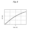
- FIG. 6 is a graph showing the magnetoresistance-external field of the transducer of FIG. 5;
- FIG. 7 is a cross-sectional, ABS view illustrating a second embodiment of the spin value type transducer according to the present invention.
- FIG. 8 is a cross-sectional, ABS view illustrating a third embodiment of the spin value type transducer according to the present invention.
- FIG. 9 is a cross-sectional, ABS view illustrating a fourth embodiment of the spin value type transducer according to the present invention.
- FIG. 10 is a cross-sectional, ABS view illustrating a fifth embodiment of the spin value type transducer according to the present invention.
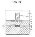
- FIGS. 11, 12, 13 , 14 and 15 are cross-sectional, ABS views illustrating modifications of the transducers of FIGS. 5, 7, 8 , 9 and 10 , respectively;
- FIG. 16 is a block circuit diagram illustrating a magnetic storage apparatus to which the transducer according to the present invention is applied.
- reference numeral 1 designates a substrate made of Al 2 O 3 .TiC which serves as a slider. Also, an about 1 ⁇ m thick lower magnetic shield layer 2 made of NiZn ferrite is deposited on the substrate 1 , and an about 30 nm thick lower gap layer (lower magnetic isolation layer) 3 made of alumina (AI 2 O 3 ) is deposited on the lower magnetic shield layer 2 .
- a spin value structure 4 is deposited on the lower gap layer 3 by a magnetron sputtering process, a radio frequency sputtering process or an ion beam sputtering process, and is patterned by an ion beam etching process.
- the spin value structure 4 will be explained later in detail.
- an about 20 nm thick permanent magnet layer 5 made of CoPt and an about 80 nm thick electrode layer 6 made of gold (Au) are formed on the lower gap layer 3 on the sides of the spin value structure 4 .
- an about 50 nm thick upper gap layer (upper magnetic isolation layer) 7 made of alumina, an about 2 ⁇ m thick upper magnetic shield layer 8 made of NiFe, an about 0.1 ⁇ m thick record gap layer 9 made of alumina and an about 2 ⁇ m thick patterned magnetic pole layer 10 made of CoFeNi are formed on the spin value structure 4 and the electrode layer 6 . Also, the magnetic pole layer 10 is coated by an alumina layer 11 .
- an exciting winding (not shown) isolated by a photoresist layer (not shown) is formed between the upper magnetic shield layer 8 and the magnetic pole layer 10 .
- the spin value structure 4 of FIG. 1 is illustrated in detail in FIGS. 2A and 2B.
- the spin value structure 4 is formed by an about 3 nm thick underlayer 41 made of Zr, an about 20 nm thick pinning layer 42 made of antiferromagnetic material such as PtMn, an about 3 nm thick pinned layer 43 made of CoFe, an about 2.1 nm thick non-magnetic conductive layer 44 made of Cu, an about 3.5 nm thick free layer 45 made of ferromagnetic material such as about 0.5 nm thick CoFe and about 3 nm thick NiFe, and an about 3 nm thick protection layer 46 made of Zr.
- FIG. 2B the sequence of the pinning layer 42 , the pinned layer 43 , the non-magnetic conductive layer 44 and the free layer 45 of FIG. 2A is reversed.
- the width of the spin value structure 4 is about 0.4 ⁇ m, and the thickness of the spin value structure 4 is about 35 nm.
- the pinning layer 42 for pinning the pinned layer 43 needs to be heat-resistant.
- PtMn is heat-resistant enough, it needs to be thicker than about 20 nm to sufficiently exhibit antiferromagnetism.
- IrMn is 7 nm thick, it can exhibit excellent antiferromagnetism, however, IrMn is not heat-resistant.
- the lower gap layer 3 is made of alumina. Since alumina is deposited by a sputtering process, it cannot be thin due to the deterioration of the insulating characteristics caused by pinholes. In order to suppress the generation of pinholes, the lower gap layer 3 needs to be at least 30 nm thick.
- the upper gap layer 7 is also made of alumina having good insulating characteristics. Besides the upper gap layer 7 needs to cover a step between the spin value structure 4 and the electrode layer 6 .
- the electrode layer 6 needs to be 80 nm thick to achieve a high signal-to-noise (S/N) ratio, even if the electrode layer 6 is made of Au. Therefore, the step between the spin value structure 4 and the electrode layer 6 is
- the upper gap layer 7 needs to be at least 50 nm.
- the resolution of a spin value type transducer is generally defined by a reproducing gap between the two magnetic shield layers, the resolution of the spin value type transistor of FIG. 1 is
- the reproducing gap is 102 nm.
- FIG. 3 which is a modification of the spin value type transducer of FIG. 1, the lower magnetic shield layer 2 of FIG. 1 is replaced by an insulating lower magnetic shield layer 2 ′, and the lower gap layer 3 of FIG. 1 is omitted. Therefore, the resolution of the spin value type transducer of FIG. 3 is
- FIG. 5 which illustrates a first embodiment of the present invention
- an about 10 nm thick magnetic isolation layer 3 A made of Cr is provided only between the permanent magnet layer 5 and the lower magnetic shield layer 2 instead of the lower gap layer 3 of FIG. 1.
- the thickness of the magnetic isolation layer 3 A is can be between 1 nm and 100 nm. That is, the spin value structure 4 is in direct contact with the lower magnetic shield layer 2 .
- the spin value structure 4 has the same configuration as illustrated in FIG. 2A.
- the upper gap layer 7 is made about 55 nm thick, since the electrode layer 6 is made about 25 nm thick and a step between the spin value structure 4 and the electrode layer 6 is a little larger. Therefore, the resolution of the spin value type transducer of FIG. 5 is
- FIG. 7 which illustrates a second embodiment of the present invention
- a spin value structure 4 A is provided instead of the spin value structure 4 of FIG. 1.
- the spin value, structure 4 A has the same configuration as illustrated in FIG. 2A except that the width of the free layer 45 and the protection layer 46 is about 0.3 ⁇ m while the width of the underlayer 41 , the pinning layer 42 , the pinned layer 43 and the nonmagnetic conductive layer 44 is the same as that of the lower magnetic shield layer 2 and the substrate 1 . Therefore, the underlayer 41 , the pinning layer 42 , the pinned layer 43 and the non-magnetic conductive layer 44 serve as the lower gap layer 3 of FIG. 1. In this case, the spin value structure 4 A is in direct contact with the lower magnetic shield layer 2 , and therefore, the resolution of the spin value type transducer of FIG. 7 is
- the spin value structure 4 has the same configuration as illustrated in FIG. 2B. Also, the electrode layer 7 is about 90 nm thick. Further, the upper gap layer 7 of FIG. 1 is not provided, so that the spin value structure 4 is in direct contact with the upper magnetic shield layer 8 . Therefore, the resolution of the spin value type transducer of FIG. 8 is
- FIG. 9 which illustrates a fourth embodiment of the present invention
- the first embodiment as illustrated in FIG. 5 is combined with the third embodiment as illustrated in FIG. 8. That is, an about 5 nm thick magnetic isolation layer 3 A made of Cr is provided only between the permanent magnet layer 5 and the lower magnetic shield layer 2 instead of the lower gap layer 3 of FIG. 1.
- the spin value structure 4 is in direct contact with the lower magnetic shield layer 2 .
- the spin value structure 4 has the same configuration as illustrated in FIG. 2A.
- the upper gap layer 7 of FIG. 1 is not provided, so that the spin value structure 4 is in direct contact with the upper magnetic layer 8 .
- the free layer 45 is on the lower side of the reproducing gap. In view of the sensitivity, it is preferable that the free layer 45 be in the center of the reproducing gap. Therefore, in FIG. 9, in order to locate the free layer 45 in the center of the reproducing gap, the thickness of the layers are made as follows:
- underlayer 41 3 nm
- pinned layer 43 2 nm
- non-magnetic conductive layer 44 2.1 nm
- free layer 45 2.5 nm (0.5 nm CoFe/2 nm NiFe)
- protection layer 46 27 nm
- the reproducing gap is 57 nm. Therefore, the resolution of the spin value type transducer of FIG. 9 is
- FIG. 10 which illustrates a fifth embodiment of the present invention
- the second embodiment as illustrated in FIG. 7 is combined with the third embodiment as illustrated in FIG. 8. That is, the spin value structure 4 A of FIG. 7 is provided instead of the spin value 4 of FIG. 1.
- the spin value structure 4 A is in direct contact with the lower magnetic shield layer 2 .
- the upper gap layer 7 of FIG. 1 is not provided, so that the spin value structure 4 is in direct contact with the upper magnetic layer 8 .
- the thickness of the layers are made as follows:
- underlayer 41 3 nm
- pinned layer 43 2 nm
- non-magnetic conductive layer 44 2.1 nm
- free layer 45 2.5 nm (0.5 nm CoFe/2 nm NiFe)
- protection layer 46 27 nm
- the reproducing gap is 57 nm. Therefore, the resolution of the spin value type transducer of FIG. 10 is
- the thickness of the layers can be made as follows:
- underlayer 41 3 nm
- non-magnetic conductive layer 44 2.1 nm
- free layer 45 2.5 nm (0.5 nm CoFe/2 nm NiFe)
- protection layer 46 22 nm
- the reproducing gap is 47 nm. Therefore, in this case, the resolution of the spin value type transducer of FIGS. 9 and 10 is
- FIGS. 11, 12, 13 , 14 and 15 which illustrate modifications of the transducers of FIGS. 5, 7, 8 , 9 and 10 , respectively, a NiZn ferrite substrate 2 A is provided instead of the Al 2 O 3 .TiC substrate 1 and the NiZn ferrite lower magnetic shield layer 2 , thus reducing the manufacturing cost.
- an about 1 ⁇ m thick lower magnetic shield layer 2 made of NiZn ferrite is deposited on a substrate 1 made of Al 2 O 3 .TiC. Note that other soft magnetic ferrite materials can be used instead of NiZn ferrite.
- a spin value structure 4 is deposited on the lower magnetic shield layer 2 by a magnetron sputtering process, a radio frequency sputtering process or an ion beam sputtering process. That is, an about 3 nm thick underlayer 41 made of Zr, an about 20 nm thick pinning layer 42 made of PtMn, an about 3 nm thick pinned layer 43 made of CoFe, an about 2.1 nm thick non-magnetic conductive layer 44 made of Cu, an about 3.5 nm thick free layer 45 made of about 0.5 nm thick CoFe and about 30 nm thick NiFe, and an about 3 nm thick protection layer 46 made of Zr are sequentially deposited on the lower magnetic shield layer 2 .
- a photoresist pattern (not shown) is formed on the spin value structure 4 .
- the spin value structure 4 is patterned by an ion beam etching process using the photoresist pattern as a mask. As a result, the spin value structure 4 is mesa-shaped due to the small ion beam scattering phenomenon.
- an about 10 nm thick magnetic gap layer (magnetic isolation layer) 3 A made of Cr, an about 25 nm thick permanent magnet layer 5 made of CoPt and an about 80 nm thick electrode layer 6 made of Au are sequentially deposited on the entire surface by an ion beam sputtering process using an Ar gas pressure of about 1.33 ⁇ 10 ⁇ 3 Pa (1 ⁇ 10 ⁇ 5 Torr) where the distance between the center of each target and a wafer rotating at 10 rpm is 25 cm.
- the Ar gas pressure is lower as compared with the other sputtering process where the Ar gas pressure is usually 1.33 ⁇ 10 ⁇ 2 Pa (1 ⁇ 10 ⁇ 4 Torr), the scattering effect of particles caused by the Ar gas can be small.
- the photoresist pattern is not heated, so that the photoresist pattern is not deformed. Then, the photoresist pattern is lifted off.
- an about 55 nm thick upper gap layer 7 made of alumina is deposited on the entire surface by a sputtering process. Then, an about 2 ⁇ m thick upper magnetic shield layer 8 made of NiFe and an about 0.1 ⁇ m thick record gap layer 9 made of alumina are sequentially deposited. Then, an about 2 ⁇ m thick magnetic pole layer 10 made of CoFeNi is formed by a plating process and is patterned. Then, an alumina layer 11 is coated.
- the spin value structure 4 is etched by using the non-magnetic conductive layer 44 as a stopper. Also, the upper magnetic shield layer 8 is formed without the formation of the upper gap layer 7 .
- the upper magnetic shield layer 8 is formed with the formation of the upper gap layer 7 .
- the lower magnetic shield layer 2 is not formed, and the spin value structure 4 or 4 A is formed directly on a NiZn ferrite substrate 2 A.
- the transducer according to the present invention is applied to a magnetic storage apparatus as illustrated in FIG. 16.
- a magnetic white/read head 1601 including the transducer according to the present invention faces a magnetic medium 1602 rotated by a motor 1603 .
- the magnetic write/read head 1601 is coupled via a suspension 1602 to an arm 1603 driven by a voice coil motor 1606 .
- the magnetic write/read head 1601 is tracked by the voice coil motor 1606 on the magnetic medium 1602 .
- the magnetic write/read head 1602 is controlled by a write/read control circuit 1607 .
- the motor 1603 , the voice coil motor 1606 and the write/read control circuit 1607 are controlled by a control unit 1608 .
- the transducer according to the present invention can have a reproducing gap of less than 0.1 ⁇ m for 500 kFCI, if the coercive force of the magnetic medium 1602 is more than 276.5 kA/m (3500 0e) and the distance between the head 1601 and the magnetic medium 1602 is less than 30 nm, the magnetic storage apparatus of FIG. 16 can have a storage capacity of more than 40 Gbits per square inch.
- the reproducing gap of a spin value type transducer can be less than 0.1 ⁇ m for 500 kFCI.
Landscapes
- Engineering & Computer Science (AREA)
- Chemical & Material Sciences (AREA)
- Nanotechnology (AREA)
- Manufacturing & Machinery (AREA)
- Physics & Mathematics (AREA)
- Crystallography & Structural Chemistry (AREA)
- Mathematical Physics (AREA)
- Theoretical Computer Science (AREA)
- Condensed Matter Physics & Semiconductors (AREA)
- General Physics & Mathematics (AREA)
- Hall/Mr Elements (AREA)
- Magnetic Heads (AREA)
Abstract
In a spin value type transducer including two magnetic shield layers, a patterned magnetoresistance element is in direct contact with one of the magnetic shield layers. A permanent magnet layer and an electrode layer are formed on the sides of the patterned magnetoresistance element.
Description
- The present invention relates to a magnetoresistance (MR) apparatus, and more particularly, to a spin value type transducer capable of reducing a reproducing gap to less than 0.1 μm.
- As magnetic storage apparatuses have been developed in size and capacity, highly sensitive magnetoresistive (MR) transducers (heads) have been put into practical use (see: Robert P. Hunt, “A Magnetoresistive Readout Transducer”, IEEE Trans. on Magnetics, Vol. MAG-7, No. 1, pp. 150-154, March 1971). Since use is made of the anisotropy magnetoresistance (AMR) effect of NiFe alloy, these MR heads are called AMR heads.
- Recently, more highly sensitive giant magnetoresistance (GMR) transducers (heads) which are called spin value type transducers, have also been developed in order to achieve higher area recording density (see: Ching Tsang et al., “Design, Fabrication & Testing of Spin-Value Read Heads for High Density Recording”, IEEE Trans. on Magnetics, Vol. 30, No. 6, pp. 3801-3806, November 1994). A typical spin value type transducer includes a spin value structure which is constructed by a free ferromagnetic layer, a pinned ferromagnetic layer and a non-magnetic conductive layer sandwiched by the free ferromagnetic layer and the pinned ferromagnetic layer, and a pinning ferromagnetic layer for pinning the magnetic domain of the pinned ferromagnetic layer. In the spin value type transducer, the resultant response is given by a cosine of an angle between the magnetization directions of the free ferromagnetic layer and the pinned ferromagnetic layer.
- A prior art spin value type transducer is constructed by two magnetic shield layers, two gap layers (magnetic isolation layers) each adhered to the inside of one of the magnetic shield layers, a spin value structure sandwiched by the gap layers, a permanent magnet layer provided at the sides of the spin value structure to provide magnetic domain control over the free ferromagnetic layer in order to suppress the Barkhausen noise, and an electrode layer formed on the permanent magnet layer (see JP-A-10-162322 & JP-A-10-149513). This will be explained later in detail.
- In the above-described prior art spin value type transducer, however, since the spin value structure is sandwiched by the two gap layers, the resolution of the transducer, i.e., a reproducing gap between the two magnetic shield layers cannot be less than 0.1 μm, which will be explained later.
- Generally, a bit length for showing the density of bits on a medium is denoted by the number of inversions of magnetic fluxes per inch, i.e., kilo flux changes per inch (kFCI). For example, if the bit length is 200 kFCI, one inversion length is 125 nm and one period is 250 nm. Therefore, the reproducing gap 0.1 μm (100 nm) is enough for 200 kFCI. Also, if the bit length is 400 kFCI, one inversion length is 62.5 nm and one period is 125 nm. Therefore, the reproducing gap 0.1 μm (100 nm) is also enough for 400 kFCI. On the other hand, if the bit length is 500 kFCI, one inversion length is 50 nm and one period is 100 nm, the reproducing gap 0.1 μm (100 nm) is insufficient for 500 kFCI.
- It is an object of the present invention to provide a spin value type transducer capable of reducing a reproducing gap to less than 0.1 μm.
- According to the present invention, in a spin value type transducer including two magnetic shield layers, a patterned magnetoresistance element is in direct contact with one of the magnetic shield layers. A permanent magnet layer and an electrode layer are formed on the sides of the patterned magnetoresistance element.
- The present invention will be more clearly understood from the description set forth below, as compared with the prior art, with reference to the accompanying drawings, wherein:
- FIG. 1 is a cross-sectional, air bearing surface (ABS) view illustrating a prior art spin value type transducer;
- FIGS. 2A and 2B are cross-sectional views of the spin value structure of FIG. 1;
- FIG. 3 is a cross-sectional view illustrating a modification of the spin value transducer of FIG. 1;
- FIG. 4 is a graph showing the magnetoresistance-external field of the transducer of FIG. 3;
- FIG. 5 is a cross-sectional, ABS view illustrating a first embodiment of the spin value type transducer according to the present invention;
- FIG. 6 is a graph showing the magnetoresistance-external field of the transducer of FIG. 5;
- FIG. 7 is a cross-sectional, ABS view illustrating a second embodiment of the spin value type transducer according to the present invention;
- FIG. 8 is a cross-sectional, ABS view illustrating a third embodiment of the spin value type transducer according to the present invention;
- FIG. 9 is a cross-sectional, ABS view illustrating a fourth embodiment of the spin value type transducer according to the present invention;
- FIG. 10 is a cross-sectional, ABS view illustrating a fifth embodiment of the spin value type transducer according to the present invention;
- FIGS. 11, 12, 13, 14 and 15 are cross-sectional, ABS views illustrating modifications of the transducers of FIGS. 5, 7, 8, 9 and 10, respectively; and
- FIG. 16 is a block circuit diagram illustrating a magnetic storage apparatus to which the transducer according to the present invention is applied.
- Before the description of the preferred embodiments, prior art spin value type transducers will be explained with reference to FIGS. 1, 2A, 2B and 3.
- In FIG. 1, which illustrates a prior art spin value type transducer (see JP-A-10-162322 & JP-A-10-149513),
reference numeral 1 designates a substrate made of Al2O3.TiC which serves as a slider. Also, an about 1 μm thick lowermagnetic shield layer 2 made of NiZn ferrite is deposited on thesubstrate 1, and an about 30 nm thick lower gap layer (lower magnetic isolation layer) 3 made of alumina (AI2O3) is deposited on the lowermagnetic shield layer 2. - A
spin value structure 4 is deposited on thelower gap layer 3 by a magnetron sputtering process, a radio frequency sputtering process or an ion beam sputtering process, and is patterned by an ion beam etching process. Thespin value structure 4 will be explained later in detail. - Also, an about 20 nm thick
permanent magnet layer 5 made of CoPt and an about 80 nmthick electrode layer 6 made of gold (Au) are formed on thelower gap layer 3 on the sides of thespin value structure 4. - Further, an about 50 nm thick upper gap layer (upper magnetic isolation layer) 7 made of alumina, an about 2 μm thick upper
magnetic shield layer 8 made of NiFe, an about 0.1 μm thickrecord gap layer 9 made of alumina and an about 2 μm thick patternedmagnetic pole layer 10 made of CoFeNi are formed on thespin value structure 4 and theelectrode layer 6. Also, themagnetic pole layer 10 is coated by analumina layer 11. - Note that an exciting winding (not shown) isolated by a photoresist layer (not shown) is formed between the upper
magnetic shield layer 8 and themagnetic pole layer 10. - The
spin value structure 4 of FIG. 1 is illustrated in detail in FIGS. 2A and 2B. - In FIG. 2A, the
spin value structure 4 is formed by an about 3 nmthick underlayer 41 made of Zr, an about 20 nmthick pinning layer 42 made of antiferromagnetic material such as PtMn, an about 3 nm thick pinnedlayer 43 made of CoFe, an about 2.1 nm thick non-magneticconductive layer 44 made of Cu, an about 3.5 nm thickfree layer 45 made of ferromagnetic material such as about 0.5 nm thick CoFe and about 3 nm thick NiFe, and an about 3 nmthick protection layer 46 made of Zr. - On the other hand, in FIG. 2B, the sequence of the
pinning layer 42, thepinned layer 43, the non-magneticconductive layer 44 and thefree layer 45 of FIG. 2A is reversed. - In FIGS. 2A and 2B, the width of the
spin value structure 4 is about 0.4 μm, and the thickness of thespin value structure 4 is about 35 nm. - Note that the
pinning layer 42 for pinning the pinnedlayer 43 needs to be heat-resistant. Although PtMn is heat-resistant enough, it needs to be thicker than about 20 nm to sufficiently exhibit antiferromagnetism. On the other hand, even if IrMn is 7 nm thick, it can exhibit excellent antiferromagnetism, however, IrMn is not heat-resistant. - As stated above, the
lower gap layer 3 is made of alumina. Since alumina is deposited by a sputtering process, it cannot be thin due to the deterioration of the insulating characteristics caused by pinholes. In order to suppress the generation of pinholes, thelower gap layer 3 needs to be at least 30 nm thick. - On the other hand, the
upper gap layer 7 is also made of alumina having good insulating characteristics. Besides theupper gap layer 7 needs to cover a step between thespin value structure 4 and theelectrode layer 6. In this case, theelectrode layer 6 needs to be 80 nm thick to achieve a high signal-to-noise (S/N) ratio, even if theelectrode layer 6 is made of Au. Therefore, the step between thespin value structure 4 and theelectrode layer 6 is - 20 nm (permanent magnet layer 5)
- +80 nm (electrode layer 6)
- +35 nm (spin value structure 4)
- =65 nm
- In order to cover the step of 65 nm, the
upper gap layer 7 needs to be at least 50 nm. - Since the resolution of a spin value type transducer is generally defined by a reproducing gap between the two magnetic shield layers, the resolution of the spin value type transistor of FIG. 1 is
- 30 nm (lower gap layer 3)
- +35 nm (spin value structure 4)
- +50 nm (upper gap layer 5)
- =115 nm
- Note that, even if the pinning
layer 42 is made of 7 nm thick IrMn, the reproducing gap is 102 nm. - Thus, in the spin value type transducer of FIG. 1, it is impossible to reduce the reproducing gap to less than 0.1 μm.
- In FIG. 3, which is a modification of the spin value type transducer of FIG. 1, the lower
magnetic shield layer 2 of FIG. 1 is replaced by an insulating lowermagnetic shield layer 2′, and thelower gap layer 3 of FIG. 1 is omitted. Therefore, the resolution of the spin value type transducer of FIG. 3 is - 35 nm (spin value structure 4)
- +50 nm (upper gap layer 5)
- =85 nm
- Thus, it is possible to reduce the reproducing gap less than 0.1 μm.
- In the spin value type transducer of FIG. 3, however, since a gap layer (magnetic isolation layer) is not provided between the
permanent magnet layer 5 and the insulating lowermagnetic shield layer 2′, the magnetic lines of force generated from thepermanent magnet layer 5 is leaked into the insulating lowermagnetic shield layer 2′, so that the magnetic domain of thefree layer 45 of thespin value structure 4 cannot be sufficiently controlled by thepermanent magnet layer 5. As a result, a large hysteresis is created in a magnetoresistance and magnetic field (R—H) loop as shown in FIG. 4, which also increases wiggled waveforms due to the Baukhausen noise in regenerated signals. - In FIG. 5, which illustrates a first embodiment of the present invention, an about 10 nm thick
magnetic isolation layer 3A made of Cr is provided only between thepermanent magnet layer 5 and the lowermagnetic shield layer 2 instead of thelower gap layer 3 of FIG. 1. Note that the thickness of themagnetic isolation layer 3A is can be between 1 nm and 100 nm. That is, thespin value structure 4 is in direct contact with the lowermagnetic shield layer 2. Also, thespin value structure 4 has the same configuration as illustrated in FIG. 2A. Note that theupper gap layer 7 is made about 55 nm thick, since theelectrode layer 6 is made about 25 nm thick and a step between thespin value structure 4 and theelectrode layer 6 is a little larger. Therefore, the resolution of the spin value type transducer of FIG. 5 is - 35 nm (spin value structure 4)
- +55 nm (upper gap layer 5)
- =90 nm
- Thus, it is possible to reduce the reproducing gap to less than 0.1 μm.
- In the spin value type transducer of FIG. 5, since the
magnetic isolation layer 3A is provided between thepermanent magnet layer 5 and the insulating lowermagnetic shield layer 2, the magnetic lines of force generated from thepermanent magnet layer 5 hardly leak into the lowermagnetic shield layer 2, so that the magnetic domain of thefree layer 45 of thespin value structure 4 can be sufficiently controlled by thepermanent magnet layer 5. As a result, no large hysteresis is created in a magnetoresistance and magnetic field (R—H) loop as shown in FIG. 6, which also decreases wiggled waveforms due to the Baukhausen noise in regenerated signals. - In FIG. 7, which illustrates a second embodiment of the present invention, a
spin value structure 4A is provided instead of thespin value structure 4 of FIG. 1. The spin value,structure 4A has the same configuration as illustrated in FIG. 2A except that the width of thefree layer 45 and theprotection layer 46 is about 0.3 μm while the width of theunderlayer 41, the pinninglayer 42, the pinnedlayer 43 and the nonmagneticconductive layer 44 is the same as that of the lowermagnetic shield layer 2 and thesubstrate 1. Therefore, theunderlayer 41, the pinninglayer 42, the pinnedlayer 43 and the non-magneticconductive layer 44 serve as thelower gap layer 3 of FIG. 1. In this case, thespin value structure 4A is in direct contact with the lowermagnetic shield layer 2, and therefore, the resolution of the spin value type transducer of FIG. 7 is - 35 nm (spin value structure 4)
- +50 nm (upper gap layer 5)
- =85 nm
- Thus, it is possible to reduce the reproducing gap to less than 0.1 μm.
- In the spin value type transducer of FIG. 7, since the non-magnetic
conductive layer 44 is provided between thepermanent magnet layer 5 and the lowermagnetic shield layer 2, the magnetic lines of force generated from thepermanent magnet layer 5 hardly leak into the lowermagnetic shield layer 2, so that the magnetic domain of thefree layer 45 of thespin value structure 4A can be sufficiently controlled by thepermanent magnet layer 5. As a result, no large hysteresis is created in a magnetoresistance and magnetic field (R—H) loop as shown in FIG. 6, which also decreases wiggled waveforms due to the Baukhausen noise in regenerated signals. - In FIG. 8, which illustrates a third embodiment of the present invention, the
spin value structure 4 has the same configuration as illustrated in FIG. 2B. Also, theelectrode layer 7 is about 90 nm thick. Further, theupper gap layer 7 of FIG. 1 is not provided, so that thespin value structure 4 is in direct contact with the uppermagnetic shield layer 8. Therefore, the resolution of the spin value type transducer of FIG. 8 is - 30 nm (lower gap layer 3)
- +35 nm (spin value structure 4)
- =65 nm
- Thus, it is possible to reduce the reproducing gap to less than 0.1 μm.
- In the spin value type transducer of FIG. 8, since the
lower gap layer 3 is provided between thepermanent magnet layer 5 and the lowermagnetic shield layer 2, the magnetic lines of force generated from thepermanent magnet layer 5 hardly leak into the lowermagnetic shield layer 2, so that the magnetic domain of thefree layer 45 of thespin value structure 4 can be sufficiently controlled by thepermanent magnet layer 5. As a result, no large hysteresis is created in a magnetoresistance and magnetic field (R—H) loop as shown in FIG. 6, which also decreases wiggled waveforms due to the Baukhausen noise in regenerated signals. Note that the magnetic lines of force generated from thepermanent magnet layer 5 toward the uppermagnetic shield layer 8 are stopped by thethin electrode layer 7. - In FIG. 9, which illustrates a fourth embodiment of the present invention, the first embodiment as illustrated in FIG. 5 is combined with the third embodiment as illustrated in FIG. 8. That is, an about 5 nm thick
magnetic isolation layer 3A made of Cr is provided only between thepermanent magnet layer 5 and the lowermagnetic shield layer 2 instead of thelower gap layer 3 of FIG. 1. As a result, thespin value structure 4 is in direct contact with the lowermagnetic shield layer 2. In this case, thespin value structure 4 has the same configuration as illustrated in FIG. 2A. On the other hand, theupper gap layer 7 of FIG. 1 is not provided, so that thespin value structure 4 is in direct contact with the uppermagnetic layer 8. - In FIG. 5, the
free layer 45 is on the lower side of the reproducing gap. In view of the sensitivity, it is preferable that thefree layer 45 be in the center of the reproducing gap. Therefore, in FIG. 9, in order to locate thefree layer 45 in the center of the reproducing gap, the thickness of the layers are made as follows: - underlayer 41: 3 nm
- pinning layer 42: 20 nm
- pinned layer 43: 2 nm
- non-magnetic conductive layer 44: 2.1 nm
- free layer 45: 2.5 nm (0.5 nm CoFe/2 nm NiFe)
- protection layer 46: 27 nm
- In this case, the reproducing gap is 57 nm. Therefore, the resolution of the spin value type transducer of FIG. 9 is
- 57 nm (spin value structure 4)
- =57 nm
- Thus, it is possible to reduce the reproducing gap to less than 0.1 μm.
- In the spin value type transducer of FIG. 9, since the
magnetic isolation layer 3A is provided between thepermanent magnet layer 5 and the insulating lowermagnetic shield layer 2, the magnetic lines of force generated from thepermanent magnet layer 5 hardly leak into the lowermagnetic shield layer 2, so that the magnetic domain of thefree layer 45 of thespin value structure 4 can be sufficiently controlled by thepermanent magnet layer 5. As a result, no large hysteresis is created in a magnetoresistance and magnetic field (R—H) loop as shown in FIG. 6, which also decreases wiggled waveforms due to the Baukhausen noise in regenerated signals. - In FIG. 10, which illustrates a fifth embodiment of the present invention, the second embodiment as illustrated in FIG. 7 is combined with the third embodiment as illustrated in FIG. 8. That is, the
spin value structure 4A of FIG. 7 is provided instead of thespin value 4 of FIG. 1. As a result, thespin value structure 4A is in direct contact with the lowermagnetic shield layer 2. On the other hand, theupper gap layer 7 of FIG. 1 is not provided, so that thespin value structure 4 is in direct contact with the uppermagnetic layer 8. - Even in FIG. 10, in order to locate the
free layer 45 in the center of the reproducing gap to improve the sensitivity, the thickness of the layers are made as follows: - underlayer 41: 3 nm
- pinning layer 42: 20 nm
- pinned layer 43: 2 nm
- non-magnetic conductive layer 44: 2.1 nm
- free layer 45: 2.5 nm (0.5 nm CoFe/2 nm NiFe)
- protection layer 46: 27 nm
- In this case, the reproducing gap is 57 nm. Therefore, the resolution of the spin value type transducer of FIG. 10 is
- 57 nm (spin value structure 4)
- =57 nm
- Thus, it is possible to reduce the reproducing gap to less than 0.1 μm.
- In the spin value type transducer of FIG. 10, since the non-magnetic
conductive layer 44 is provided between thepermanent magnet layer 5 and the insulating lowermagnetic shield layer 2, the magnetic lines of force generated from thepermanent magnet layer 5 hardly leak into the lowermagnetic shield layer 2, so that the magnetic domain of thefree layer 45 of thespin value structure 4 can be sufficiently controlled by thepermanent magnet layer 5. As a result, no large hysteresis is created in a magnetoresistance and magnetic field (R—H) loop as shown in FIG. 6, which also decreases wiggled waveforms due to the Baukhausen noise in regenerated signals. - In the transducers of FIGS. 9 and 10, the thickness of the layers can be made as follows:
- underlayer 41: 3 nm
- pinning layer 42: 15 nm
- pinned layer 43: 2 nm
- non-magnetic conductive layer 44: 2.1 nm
- free layer 45: 2.5 nm (0.5 nm CoFe/2 nm NiFe)
- protection layer 46: 22 nm
- In this case, the reproducing gap is 47 nm. Therefore, in this case, the resolution of the spin value type transducer of FIGS. 9 and 10 is
- 47 nm (spin value structure 4)
- =47 nm
- Thus, it is possible to reduce the reproducing gap less than 0.05 μm, which is sufficient for 1000 kFCI where one inversion length is 25 nm and one period is 50 nm.
- In FIGS. 11, 12, 13, 14 and 15, which illustrate modifications of the transducers of FIGS. 5, 7, 8, 9 and 10, respectively, a
NiZn ferrite substrate 2A is provided instead of the Al2O3.TiC substrate 1 and the NiZn ferrite lowermagnetic shield layer 2, thus reducing the manufacturing cost. - The method for manufacturing the transducer of FIG. 5 is explained below.
- First, an about 1 μm thick lower
magnetic shield layer 2 made of NiZn ferrite is deposited on asubstrate 1 made of Al2O3.TiC. Note that other soft magnetic ferrite materials can be used instead of NiZn ferrite. - Next, a
spin value structure 4 is deposited on the lowermagnetic shield layer 2 by a magnetron sputtering process, a radio frequency sputtering process or an ion beam sputtering process. That is, an about 3 nmthick underlayer 41 made of Zr, an about 20 nm thick pinninglayer 42 made of PtMn, an about 3 nm thick pinnedlayer 43 made of CoFe, an about 2.1 nm thick non-magneticconductive layer 44 made of Cu, an about 3.5 nm thickfree layer 45 made of about 0.5 nm thick CoFe and about 30 nm thick NiFe, and an about 3 nmthick protection layer 46 made of Zr are sequentially deposited on the lowermagnetic shield layer 2. - Next, a photoresist pattern (not shown) is formed on the
spin value structure 4. Then, thespin value structure 4 is patterned by an ion beam etching process using the photoresist pattern as a mask. As a result, thespin value structure 4 is mesa-shaped due to the small ion beam scattering phenomenon. - Next, an about 10 nm thick magnetic gap layer (magnetic isolation layer) 3A made of Cr, an about 25 nm thick
permanent magnet layer 5 made of CoPt and an about 80 nmthick electrode layer 6 made of Au are sequentially deposited on the entire surface by an ion beam sputtering process using an Ar gas pressure of about 1.33×10⁻³ Pa (1×10⁻⁵ Torr) where the distance between the center of each target and a wafer rotating at 10 rpm is 25 cm. In this case, since the Ar gas pressure is lower as compared with the other sputtering process where the Ar gas pressure is usually 1.33×10⁻² Pa (1×10⁻⁴ Torr), the scattering effect of particles caused by the Ar gas can be small. Also, since the distance between each target and the wafer is large, the direction of particles deposited on the wafer can be uniform. Further, since no plasma gas is present on the surface of the wafer in the ion beam sputtering process, the photoresist pattern is not heated, so that the photoresist pattern is not deformed. Then, the photoresist pattern is lifted off. - Next, an about 55 nm thick
upper gap layer 7 made of alumina is deposited on the entire surface by a sputtering process. Then, an about 2 μm thick uppermagnetic shield layer 8 made of NiFe and an about 0.1 μm thickrecord gap layer 9 made of alumina are sequentially deposited. Then, an about 2 μm thickmagnetic pole layer 10 made of CoFeNi is formed by a plating process and is patterned. Then, analumina layer 11 is coated. - When manufacturing the transducers of FIGS. 7, 10, 12 and 15, the
spin value structure 4 is etched by using the non-magneticconductive layer 44 as a stopper. Also, the uppermagnetic shield layer 8 is formed without the formation of theupper gap layer 7. - When manufacturing the transducers of FIGS. 8, 9, 10, 13, 14 and 15, the upper
magnetic shield layer 8 is formed with the formation of theupper gap layer 7. - When manufacturing the transducers of FIGS. 11, 12, 13, 14 and 15, the lower
magnetic shield layer 2 is not formed, and thespin value structure NiZn ferrite substrate 2A. - The transducer according to the present invention is applied to a magnetic storage apparatus as illustrated in FIG. 16. In FIG. 16, a magnetic white/
read head 1601 including the transducer according to the present invention faces a magnetic medium 1602 rotated by amotor 1603. The magnetic write/read head 1601 is coupled via asuspension 1602 to anarm 1603 driven by avoice coil motor 1606. Thus, the magnetic write/read head 1601 is tracked by thevoice coil motor 1606 on themagnetic medium 1602. The magnetic write/read head 1602 is controlled by a write/read control circuit 1607. Also, themotor 1603, thevoice coil motor 1606 and the write/read control circuit 1607 are controlled by acontrol unit 1608. As explained above, the transducer according to the present invention can have a reproducing gap of less than 0.1 μm for 500 kFCI, if the coercive force of the magnetic medium 1602 is more than 276.5 kA/m (3500 0e) and the distance between thehead 1601 and the magnetic medium 1602 is less than 30 nm, the magnetic storage apparatus of FIG. 16 can have a storage capacity of more than 40 Gbits per square inch. - According to the present invention, the reproducing gap of a spin value type transducer can be less than 0.1 μm for 500 kFCI.
Claims (54)
1. A spin value type transducer comprising:
two magnetic shield layers;
a patterned magnetoresistance element in direct contact with one of said two shield layers;
a permanent magnet layer formed on sides of said patterned magnetoresistance element; and an
an electrode layer formed on the sides of said patterned magnetoresistance element.
2. The transducer as set forth in claim 1 , wherein said one of said magnetic shield layers in direct contact with said magnetoresistance element is made of insulating material.
3. The apparatus as set forth in claim 1 , wherein a reproducing gap between said two magnetic shield layers is less than 0.1 μm.
4. The transducer as set forth in claim 1 , further comprising a magnetic isolation layer interposed between said one of said magnetic shield layers in direct contact with said magnetoresistance element and said permanent magnet layer.
5. The transducer as set forth in claim 4 , where a thickness of said magnetic isolation layer is between 1 nm and 100 nm.
6. The transducer as set forth in claim 1 , wherein said patterned magnetoresistance element comprises a patterned portion connected to ends of said permanent magnet layer and said electrode layer and a non-patterned portion interposed between said one of said magnetic shield layers and said electrode layer.
7. The transducer as set forth in claim 1 , further comprising a non-magnetic insulating substrate on which said one of said magnetic shield layers is formed.
8. The transducer as set forth in claim 7 , wherein said one of said magnetic shield layers formed on said non-magnetic substrate is made of soft-magnetic ferrite.
9. The transducer as set forth in claim 1 , wherein said one of said magnetic shield layers comprises a non-magnetic insulating substrate.
10. The transducer as set forth in claim 1 , wherein one of said magnetic shield layers comprises an insulating substrate made of soft magnetic ferrite.
11. The transducer as set forth in claim 1 , wherein said patterned magnetoresistance element comprises:
a pinning layer made of antiferromagnetic material;
a pinned layer made of ferromagnetic material adhered to said pinning layer;
a free layer made of ferromagnetic material; and
a non-magnetic conductive layer sandwiched by said pinned layer and said free layer.
12. The transducer as set forth in claim 6 , wherein said patterned magnetoresistance element comprises:
a pinning layer made of antiferromagnetic material;
a pinned layer made of ferromagnetic material adhered to said pinning layer;
a free layer made of ferromagnetic material; and
a non-magnetic conductive layer sandwiched by said pinned layer and said free layer,
said patterned portion being formed by said free layer,
said non-patterned portion being formed by said pinning layer, said pinned layer and said non-magnetic conductive layer.
13. A spin value type transducer comprising:
first and second magnetic shield layers;
a patterned magnetoresistance element in direct contact with said first shield layer;
a magnetic isolation layer formed on sides of said patterned magnetoresistance element in direct contact with said first magnetic shield layer;
a permanent magnet layer formed on said magnetic isolation layer; and
an electrode layer formed on said permanent magnet layer.
14. The transducer as set forth in claim 13 , further comprising a gap layer interposed between said magnetoresistance element and said second magnetic shield layer and between said electrode layer and said second magnetic shield layer.
15. The transducer as set forth in claim 13 , wherein said second magnetic shield layer is in direct contact with said magnetoresistance element and said electrode layer.
16. The transducer as set forth in claim 13 , wherein of said first magnetic shield layer is made of insulating material.
17. The transducer as set forth in claim 13 , wherein a reproducing gap between said first and second magnetic shield layers is less than 0.1 μm.
18. The transducer as set forth in claim 13 , wherein a thickness of said magnetic isolation layer is between 1 nm and 100 nm.
19. The transducer as set forth in claim 13 , further comprising a non-magnetic insulating substrate on which said first magnetic shield layer is formed.
20. The transducer as set forth in claim 19 , wherein said first magnetic shield layer is made of soft-magnetic ferrite.
21. The transducer as set forth in claim 13 , wherein said first magnetic shield layer comprises a non-magnetic substrate.
22. The transducer as set forth in claim 13 , wherein said first magnetic shield layer comprises an insulating substrate made of soft magnetic ferrite.
23. The transducer as set forth in claim 13 , wherein said patterned magnetoresistance element comprises:
a pinning layer made of antiferromagnetic material;
a pinned layer made of ferromagnetic material adhered to said pinning layer;
a free layer made of ferromagnetic material; and
a non-magnetic conductive layer sandwiched by said pinned layer and said free layer.
24. A spin value type transducer comprising:
first and second magnetic shield layers;
a magnetoresistance element including a patterned portion and a non-patterned portion in direct contact with said first shield layer;
a permanent magnet layer formed on said non-patterned portion of said magnetoresistance element; and
an electrode layer formed on said permanent magnet layer.
25. The transducer as set forth in claim 24 , further comprising a gap layer interposed between said patterned portion of said magnetoresistance element and said second magnetic shield layer and between said electrode layer and said second magnetic shield layer.
26. The transducer as set forth in claim 24 , wherein said second magnetic shield layer is in direct contact with said patterned portion of said magnetoresistance element and said electrode layer.
27. The transducer as set forth in claim 24 , wherein said first magnetic shield layer is made of insulating material.
28. The transducer as set forth in claim 24 , wherein a reproducing gap between said first and second magnetic shield layers is less than 0.1 μm.
29. The transducer as set forth in claim 24 , further comprising a non-magnetic insulating substrate on which said first magnetic shield layer is formed.
30. The transducer as set forth in claim 29 , wherein said first magnetic shield layer is made of soft-magnetic ferrite.
31. The transducer as set forth in claim 24 , wherein said first magnetic shield layer comprises a non-magnetic substrate.
32. The transducer as set forth in claim 24 , wherein said first magnetic shield layer comprises an insulating substrate made of soft magnetic ferrite.
33. The transducer as set forth in claim 6 , wherein said patterned magnetoresistance element comprises:
a pinning layer made of antiferromagnetic material;
a pinned layer made of ferromagnetic material adhered to said pinning layer;
a free layer made of ferromagnetic material; and
a non-magnetic conductive layer sandwiched by said pinned layer and said free layer,
said patterned portion being formed by said free layer,
said non-patterned portion being formed by said pinning layer, said pinned layer and said non-magnetic conductive layer.
34. A spin value type transducer comprising:
first and second magnetic shield layers;
a gap layer formed on said first magnetic shield layer;
a patterned magnetoresistance element in direct contact with said gap layer;
a permanent magnet layer formed on sides of said patterned magnetoresistance element; and
an electrode layer formed on said permanent magnet layer,
said second magnetic shield layer is in direct contact with said magnetoresistance element and said electrode layer.
35. The transducer as set forth in claim 34 , wherein said first magnetic shield layer is made of insulating material.
36. The transducer as set forth in claim 34 , wherein a reproducing gap between said first and second magnetic shield layers is less than 0.1 μm.
37. The transducer as set forth in claim 34 , further comprising a non-magnetic insulating substrate on which said first magnetic shield layer is formed.
38. The transducer as set forth in claim 37 , wherein said first magnetic shield layer is made of soft-magnetic ferrite.
39. The transducer as set forth in claim 34 , wherein said first magnetic shield layers comprises a non-magnetic insulating substrate.
40. The transducer as set forth in claim 34 , wherein said first magnetic shield layer comprises an insulating substrate made of soft magnetic ferrite.
41. The transducer as set forth in claim 34 , wherein said patterned magnetoresistance element comprises:
a pinning layer made of antiferromagnetic material;
a pinned layer made of ferromagnetic material adhered to said pinning layer;
a free layer made of ferromagnetic material; and
a non-magnetic conductive layer sandwiched by said pinned layer and said free layer.
42. A magnetic storage apparatus including a magnetic write head, a magnetic read head and a magnetic medium, said magnetic read head comprising:
two magnetic shield layers;
a patterned magnetoresistance element in direct contact with one of said two shield layers;
a permanent magnet layer formed on sides of said patterned magnetoresistance element; and
an electrode layer formed on the sides of said patterned magnetoresistance element.
43. The apparatus as set forth in claim 42 , wherein said one of said magnetic shield layers in direct contact with said magnetoresistance element is made of insulating material.
44. The apparatus as set forth in claim 41 , wherein a reproducing gap between said two magnetic shield layers is less than 0.1 μm.
45. The apparatus as set forth in claim 42 , wherein said magnetic read head further comprises a magnetic isolation layer interposed between said one of said magnetic shield layers in direct contact with said magnetoresistance element and said permanent magnet layer.
46. The apparatus as set forth in claim 45 , where a thickness of said magnetic isolation layer is between 1 nm and 100 nm.
47. The apparatus as set forth in claim 42 , wherein said patterned magnetoresistance element comprises a patterned portion connected to ends of said permanent magnet layer and said electrode layer and a non-patterned portion interposed between said one of said magnetic shield layers and said electrode layer.
48. The apparatus as set forth in claim 42 , further comprising a non-magnetic insulating substrate on which said one of said magnetic shield layers is formed.
49. The apparatus as set forth in claim 48 , wherein said one of said magnetic shield layers formed on said non-magnetic substrate is made of soft-magnetic ferrite.
50. The apparatus as set forth in claim 42 , wherein said one of said magnetic shield layers comprises a non-magnetic substrate.
51. The apparatus as set forth in claim 42 , wherein said one of said magnetic shield layers comprises an insulating substrate made of soft magnetic ferrite.
52. The apparatus as set forth in claim 42 , wherein said patterned magnetoresistance element comprises:
a pinning layer made of antiferromagnetic material;
a pinned layer made of ferromagnetic material adhered to said pinning layer;
a free layer made of ferromagnetic material; and
a non-magnetic conductive layer sandwiched by said pinned layer and said free layer.
53. The apparatus as set forth in claim 47 , wherein said patterned magnetoresistance element comprises:
a pinning layer made of antiferromagnetic material;
a pinned layer made of ferromagnetic material adhered to said pinning layer;
a free layer made of ferromagnetic material; and
a non-magnetic conductive layer sandwiched by said pinned layer and said free layer,
said patterned portion being formed by said free layer,
said non-patterned portion being formed by said pinning layer, said pinned layer and said non-magnetic conductive layer.
54. The apparatus as set forth in claim 42 , wherein a distance between said magnetic read head and said magnetic medium is less than about 30 nm.
Priority Applications (2)
| Application Number | Priority Date | Filing Date | Title |
|---|---|---|---|
| US10/446,106 US6754051B2 (en) | 1999-03-24 | 2003-05-28 | Spin valve transducer having partly patterned magnetoresistance element |
| US10/835,399 US7079360B2 (en) | 1999-03-24 | 2004-04-30 | Spin valve transducer having partly patterned magnetoresistance element |
Applications Claiming Priority (5)
| Application Number | Priority Date | Filing Date | Title |
|---|---|---|---|
| JP11079977A JP2000276716A (en) | 1999-03-24 | 1999-03-24 | Magnetoresistance effect type head, its manufacture and magnetic storage device |
| JP11-079977 | 1999-03-24 | ||
| JP079977/1999 | 1999-03-24 | ||
| US09/532,444 US7085109B1 (en) | 1999-03-24 | 2000-03-23 | Spin valve type transducer capable of reducing reproducing gap |
| US10/446,106 US6754051B2 (en) | 1999-03-24 | 2003-05-28 | Spin valve transducer having partly patterned magnetoresistance element |
Related Parent Applications (1)
| Application Number | Title | Priority Date | Filing Date |
|---|---|---|---|
| US09/532,444 Division US7085109B1 (en) | 1999-03-24 | 2000-03-23 | Spin valve type transducer capable of reducing reproducing gap |
Related Child Applications (1)
| Application Number | Title | Priority Date | Filing Date |
|---|---|---|---|
| US10/835,399 Division US7079360B2 (en) | 1999-03-24 | 2004-04-30 | Spin valve transducer having partly patterned magnetoresistance element |
Publications (2)
| Publication Number | Publication Date |
|---|---|
| US20030197981A1 true US20030197981A1 (en) | 2003-10-23 |
| US6754051B2 US6754051B2 (en) | 2004-06-22 |
Family
ID=13705397
Family Applications (3)
| Application Number | Title | Priority Date | Filing Date |
|---|---|---|---|
| US09/532,444 Expired - Fee Related US7085109B1 (en) | 1999-03-24 | 2000-03-23 | Spin valve type transducer capable of reducing reproducing gap |
| US10/446,106 Expired - Lifetime US6754051B2 (en) | 1999-03-24 | 2003-05-28 | Spin valve transducer having partly patterned magnetoresistance element |
| US10/835,399 Expired - Fee Related US7079360B2 (en) | 1999-03-24 | 2004-04-30 | Spin valve transducer having partly patterned magnetoresistance element |
Family Applications Before (1)
| Application Number | Title | Priority Date | Filing Date |
|---|---|---|---|
| US09/532,444 Expired - Fee Related US7085109B1 (en) | 1999-03-24 | 2000-03-23 | Spin valve type transducer capable of reducing reproducing gap |
Family Applications After (1)
| Application Number | Title | Priority Date | Filing Date |
|---|---|---|---|
| US10/835,399 Expired - Fee Related US7079360B2 (en) | 1999-03-24 | 2004-04-30 | Spin valve transducer having partly patterned magnetoresistance element |
Country Status (2)
| Country | Link |
|---|---|
| US (3) | US7085109B1 (en) |
| JP (1) | JP2000276716A (en) |
Cited By (2)
| Publication number | Priority date | Publication date | Assignee | Title |
|---|---|---|---|---|
| US20070025026A1 (en) * | 2005-07-28 | 2007-02-01 | Hitachi Global Storage Technologies | Thin shield structure for reduced protrusion in a magnetoresistive head |
| EP2662856A4 (en) * | 2011-01-07 | 2017-08-30 | Multidimension Technology Co., Ltd | Thin-film magnetoresistance sensing element, combination thereof, and electronic device coupled to the combination |
Families Citing this family (5)
| Publication number | Priority date | Publication date | Assignee | Title |
|---|---|---|---|---|
| JP2000276716A (en) * | 1999-03-24 | 2000-10-06 | Nec Corp | Magnetoresistance effect type head, its manufacture and magnetic storage device |
| US6879471B2 (en) * | 2003-06-17 | 2005-04-12 | Seagate Technology Llc | Recording head design for identifying reader-to-permanent magnet isolation failure |
| US7270854B2 (en) * | 2003-11-19 | 2007-09-18 | Hitachi Global Storage Technologies Netherlands B.V. | Method for forming a head having improved spin valve properties |
| KR100832583B1 (en) * | 2007-01-04 | 2008-05-27 | 한국과학기술연구원 | Spin Transistor Using Leakage Field |
| US8305715B2 (en) * | 2007-12-27 | 2012-11-06 | HGST Netherlands, B.V. | Magnetoresistance (MR) read elements having an active shield |
Citations (2)
| Publication number | Priority date | Publication date | Assignee | Title |
|---|---|---|---|---|
| US5910870A (en) * | 1996-11-15 | 1999-06-08 | Nec Corporation | Magnetoresistive effect composite head with laminated magnetic layer isolated from magnetic pole layer |
| US6125009A (en) * | 1996-11-28 | 2000-09-26 | Nec Corporation | Magnetoresistive effect composite head having a pole containing Co-M |
Family Cites Families (14)
| Publication number | Priority date | Publication date | Assignee | Title |
|---|---|---|---|---|
| US4044392A (en) * | 1975-08-14 | 1977-08-23 | International Business Machines Corporation | Process for making a read-while-write tape head and the product made thereby |
| JPS58189819A (en) | 1982-04-30 | 1983-11-05 | Nec Corp | Magneto-resistance effect head |
| JPS60113313A (en) * | 1983-11-22 | 1985-06-19 | Nec Corp | Magneto-resistance effect head |
| US4663684A (en) * | 1984-01-27 | 1987-05-05 | Hitachi, Ltd. | Magnetic transducer using magnetoresistance effect |
| JP2613239B2 (en) * | 1988-02-26 | 1997-05-21 | 株式会社日立製作所 | Magnetoresistive head |
| JPH06274834A (en) | 1993-03-24 | 1994-09-30 | Sumitomo Metal Ind Ltd | Thin film magnetic head and manufacturing method thereof |
| JPH0855310A (en) | 1994-08-12 | 1996-02-27 | Sumitomo Metal Ind Ltd | Magnetoresistive head |
| US5434826A (en) * | 1994-09-26 | 1995-07-18 | Read-Rite Corporation | Multilayer hard bias films for longitudinal biasing in magnetoresistive transducer |
| JPH08124122A (en) | 1994-10-25 | 1996-05-17 | Hitachi Ltd | Magnetoresistive reproducing head and magnetic recording / reproducing apparatus |
| JP3130811B2 (en) * | 1996-11-28 | 2001-01-31 | 日本電気株式会社 | Magnetoresistive thin film magnetic head |
| JPH10283617A (en) | 1997-04-04 | 1998-10-23 | Minebea Co Ltd | Composite head for perpendicular magnetic recording |
| JPH10289423A (en) | 1997-04-10 | 1998-10-27 | Minebea Co Ltd | Manufacture of combined type head for vertical magnetic recording |
| JP2000276716A (en) * | 1999-03-24 | 2000-10-06 | Nec Corp | Magnetoresistance effect type head, its manufacture and magnetic storage device |
| US6700752B2 (en) * | 2001-04-18 | 2004-03-02 | Seagate Technology Llc | Non-magnetic metallic layer in a reader gap of a disc drive |
-
1999
- 1999-03-24 JP JP11079977A patent/JP2000276716A/en active Pending
-
2000
- 2000-03-23 US US09/532,444 patent/US7085109B1/en not_active Expired - Fee Related
-
2003
- 2003-05-28 US US10/446,106 patent/US6754051B2/en not_active Expired - Lifetime
-
2004
- 2004-04-30 US US10/835,399 patent/US7079360B2/en not_active Expired - Fee Related
Patent Citations (2)
| Publication number | Priority date | Publication date | Assignee | Title |
|---|---|---|---|---|
| US5910870A (en) * | 1996-11-15 | 1999-06-08 | Nec Corporation | Magnetoresistive effect composite head with laminated magnetic layer isolated from magnetic pole layer |
| US6125009A (en) * | 1996-11-28 | 2000-09-26 | Nec Corporation | Magnetoresistive effect composite head having a pole containing Co-M |
Cited By (3)
| Publication number | Priority date | Publication date | Assignee | Title |
|---|---|---|---|---|
| US20070025026A1 (en) * | 2005-07-28 | 2007-02-01 | Hitachi Global Storage Technologies | Thin shield structure for reduced protrusion in a magnetoresistive head |
| US7652853B2 (en) * | 2005-07-28 | 2010-01-26 | Hitachi Global Storage Technologies Netherlands B.V. | Thin shield structure for reduced protrusion in a magnetoresistive head |
| EP2662856A4 (en) * | 2011-01-07 | 2017-08-30 | Multidimension Technology Co., Ltd | Thin-film magnetoresistance sensing element, combination thereof, and electronic device coupled to the combination |
Also Published As
| Publication number | Publication date |
|---|---|
| US20040201927A1 (en) | 2004-10-14 |
| US7085109B1 (en) | 2006-08-01 |
| US7079360B2 (en) | 2006-07-18 |
| JP2000276716A (en) | 2000-10-06 |
| US6754051B2 (en) | 2004-06-22 |
Similar Documents
| Publication | Publication Date | Title |
|---|---|---|
| US6542342B1 (en) | Magnetoresistive effect transducer having longitudinal bias layer directly connected to free layer | |
| US6452204B1 (en) | Tunneling magnetoresistance transducer and method for manufacturing the same | |
| KR100440032B1 (en) | Magneto resistance effect element, magneto resistance effect head, magneto resistance transducer system, and magnetic storage system | |
| US6724585B2 (en) | Magnetoresistive element and device utilizing magnetoresistance effect | |
| US7116530B2 (en) | Thin differential spin valve sensor having both pinned and self pinned structures for reduced difficulty in AFM layer polarity setting | |
| JP3760095B2 (en) | Two-element reproducing sensor, thin film magnetic head for perpendicular magnetic recording / reproducing, and perpendicular magnetic recording / reproducing apparatus | |
| KR19990083593A (en) | Spin tunnel magneto-resistance effect type magnetic sensor and production method thereof | |
| KR20000016943A (en) | Low moment/high coercivity pinned layer for magnetic tunnel junction sensors | |
| KR20010062412A (en) | Magneto-resistance effect head and magnetic storage device employing the head | |
| JP2000215415A (en) | Magnetoresistance effect element | |
| JP2001325704A (en) | Magnetoresistive effect sensor, method for manufacturing the same, magnetic resistance detecting system and magnetic storage system | |
| JP3680655B2 (en) | Magnetoresistive element and manufacturing method thereof | |
| JPH10289417A (en) | Thin film magnetic head | |
| JP3989368B2 (en) | Magnetic head and magnetic recording apparatus | |
| US6270588B1 (en) | Magnetoresistive effect sensor, thin-film magnetic head with the sensor and manufacturing method of the thin-film magnetic head | |
| US7085109B1 (en) | Spin valve type transducer capable of reducing reproducing gap | |
| US6665153B1 (en) | Magnetoresistance element, head, sensing system, and magnetic storing system | |
| JPH1091920A (en) | Magneto-resistance effect type head | |
| JP2000293823A (en) | Magneto-resistance effect element, its production, magneto-resistance effect head, and magnetic recording and reproducing device | |
| JPH10302227A (en) | Magnetoresistive head | |
| JPH0944819A (en) | Magnetic conversion element and thin-film magnetic head | |
| JP2000076629A (en) | Magnetoresistive effect type head, its manufacture and magnetic storage device | |
| US20040134877A1 (en) | magnetoresistance apparatus having reduced overlapping of permanent magnet layer and method for manufacturing the same | |
| JP2000276714A (en) | Spin valve sensor that fixes magnetization with current | |
| JPH09305924A (en) | Magneto-resistance effect type magneto-sensitive element and magnetic head using the same |
Legal Events
| Date | Code | Title | Description |
|---|---|---|---|
| STCF | Information on status: patent grant |
Free format text: PATENTED CASE |
|
| FPAY | Fee payment |
Year of fee payment: 4 |
|
| FEPP | Fee payment procedure |
Free format text: PAYOR NUMBER ASSIGNED (ORIGINAL EVENT CODE: ASPN); ENTITY STATUS OF PATENT OWNER: LARGE ENTITY |
|
| FPAY | Fee payment |
Year of fee payment: 8 |
|
| FPAY | Fee payment |
Year of fee payment: 12 |