US20030197624A1 - Method and device for receiving sequential instructions - Google Patents
Method and device for receiving sequential instructions Download PDFInfo
- Publication number
- US20030197624A1 US20030197624A1 US10/124,040 US12404002A US2003197624A1 US 20030197624 A1 US20030197624 A1 US 20030197624A1 US 12404002 A US12404002 A US 12404002A US 2003197624 A1 US2003197624 A1 US 2003197624A1
- Authority
- US
- United States
- Prior art keywords
- instruction
- instructions
- response
- time
- receiving
- Prior art date
- Legal status (The legal status is an assumption and is not a legal conclusion. Google has not performed a legal analysis and makes no representation as to the accuracy of the status listed.)
- Granted
Links
Images


Classifications
-
- G—PHYSICS
- G08—SIGNALLING
- G08C—TRANSMISSION SYSTEMS FOR MEASURED VALUES, CONTROL OR SIMILAR SIGNALS
- G08C23/00—Non-electrical signal transmission systems, e.g. optical systems
- G08C23/04—Non-electrical signal transmission systems, e.g. optical systems using light waves, e.g. infrared
Definitions
- the present invention relates to a method and/or architecture for receiving sequential instructions generally and, more particularly, to rejecting instructions with improper timing relative to an initial instruction.
- Infrared (IR) remote control devices are commonly used to transmit instructions to receivers in consumer electronics such as televisions, radios, cameras, video cassette recorders, and digital versatile disc (DVD) players.
- the IR remote control devices use infrared light pulses to transmit instructions to the receiver in accordance with a standard protocol.
- a standard protocol According to an NEC Corporation standard protocol, when a key of the remote control is pressed and held for a while, a set of pulses indicating a repeat key instruction (i.e., REP_KEY) is sent after a train of pulses that carries coded information for an instruction (i.e., KEY_A) of the key being pressed.
- REP_KEY repeat key instruction
- the receiver interprets the repeat key instruction REP_KEY by repeating a most recently received non-repeat key instruction. For example, reception of the instruction KEY_A followed by three repeat key instructions REP_KEY will be interpreted as a sequence of four instructions KEY_A.
- a rate of repeating it is also desirable for a rate of repeating to vary for different keys.
- a volume instruction and a string of repeat key instructions REP_KEY will be transmitted and received at a fixed rate when the user presses and holds a volume-up key.
- a channel increment instruction and another string of repeat key instructions REP_KEY will be transmitted and received at the same fixed rate.
- the manufacturer and the user commonly want the volume to increase at a slow rate for fine control and the television channel to increment quickly for rapid scrolling. With the fixed repeat rate for all repeat key instructions REP_KEY, the volume and channel change at the same rate.
- the present invention concerns a method of receiving a plurality of instructions.
- the method generally comprises the steps of (A) storing a first of the instructions in response to receiving the first instruction at an initial time, and (B) rejecting a second of the instructions that depends from the first instruction in response to receiving the second instruction greater than a maximum delay after the initial time.
- the objects, features and advantages of the present invention include providing a method and/or architecture for receiving sequential instructions that may (i) discard false repeat instructions, (ii) disable acceptance of repeat instructions for predetermined key presses, (iii) provide for variable periods to consider a repeat instruction valid, (iv) vary an expected time when a new repeat instruction will be received, and/or (v) dynamically update repeat key characteristics at run time.
- FIG. 1 is a block diagram of a device implementing a preferred embodiment of the present invention
- FIG. 2 is an example waveform of instructions
- FIG. 3 is an example waveform of a non-repeat key
- FIG. 4 is a detailed example waveform of a portion of the non-repeat key instruction
- FIG. 5 is an example waveform of a repeat key
- FIG. 6 is an example waveform of a carrier
- FIG. 7 is a detailed block diagram of a receiver circuit
- FIG. 8 is a flow diagram for a method of operation.
- the device 100 may be implemented as an infrared (IR) remote control receiver configured to receive a signal (e.g., REC).
- IR infrared
- the device 100 generally comprises a sensor 102 , a receiver circuit 104 and a clock circuit 106 .
- the sensor 102 may have an input 108 to receive the signal REC.
- An output 110 of the sensor 102 may be coupled to an input 112 of the receiver circuit 104 to transfer a signal (e.g., PULSE).
- the receiver circuit 104 may have an output 114 to present a signal (e.g., INSTR).
- the receiver 104 may have another output 116 to present another signal (e.g., STATUS).
- An input 118 of the receiver circuit 104 may be coupled to an output 120 of the clock circuit 106 to receive a signal (e.g., CURRENT_TIME).
- the signal REC may be implemented as an optical signal.
- the optical signal REC may be implemented as an infrared (IR) optical signal.
- the optical signal REC may transfer codes or instructions from a remote control 122 to the device 100 .
- the instructions may provide parameters for the operation of the device 100 .
- the instructions may be pulse encoded within the optical signal REC.
- the optical signal REC may be implemented as other types of signals, for example radio-frequency, acoustic and electrical, to meet the design criteria of a particular application.
- the signal PULSE may be implemented as an electrical signal.
- the electrical signal PULSE may be an electrical version of the optical signal REC.
- the electrical signal PULSE may transfer the same instruction carried by the optical signal REC.
- the instructions may be pulse encoded within the electrical signal PULSE.
- the signal INSTR may be implemented as a decoded instruction signal.
- the signal INSTR may carry the instructions decoded from the signal PULSE. A unique value may be used to identify each type of instruction presented by the signal INSTR.
- the signal STATUS may be implemented as a status signal.
- the signal STATUS may provide additional information about the signal INSTR.
- a valid state may be provided in the signal STATUS while the signal INSTR contains a valid or accepted instruction.
- An invalid state may be provided in the signal STATUS while the signal INSTR contains an invalid or rejected instruction.
- the invalid state information may be presented in the signal INSTR as a special code while all other codes are presumed to be valid.
- the signal INSTR may be suppressed by the receiver circuit 104 while the signal STATUS simultaneously conveys the invalid state.
- the signal CURRENT_TIME may be implemented as a time signal.
- the signal CURRENT_TIME may provide a time value to the receiver circuit 104 that updates on a periodic basis.
- the length of a period is generally less than a time duration for receiving an instruction within the signal REC.
- the sensor 102 may be operational to convert the signal REC to the signal PULSE. Different types of sensors 102 may be implemented to match the type (e.g., optical, radio-frequency, etc.) of signal REC.
- the receiver circuit 104 may be operational to accept or reject instructions within the signal PULSE based upon (i) the type of instruction received, (ii) a previously received instructions, (iii) a time of reception as determined by the signal CURRENT_TIME, and/or (iv) a value of a disable signal allocated to each type of instruction.
- the clock circuit 106 may be configured to generate the signal CURRENT_TIME.
- the instructions conveyed by the signals REC, PULSE and INSTR may be generally categorized as repeat instructions and non-repeat instructions.
- a unique non-repeat instruction is generally generated and transmitted by the remove control 122 for each key press detected by the remote control 122 .
- Examples of non-repeat instructions may include, but are not limited to, volume increase, volume decrease, channel increase, channel decrease, 0, 1, 2, 3, 4, 5, 6, 7, 8, 9, 0, play, stop, fast forward, reverse, pause, record and the like.
- Repeat instructions generally depend on a previously received non-repeat instruction.
- One or more repeat instructions may follow any non-repeat instruction while a selected key of the remote control circuit 122 remains pressed.
- the device 100 may interpret each received repeat instruction as if a duplicate of a last received non-repeat instruction had been received. For example, a volume increase instruction followed by five repeat instructions may be treated as six consecutive volume increase instructions.
- the waveform 124 generally comprises a non-repeat instruction (e.g., New Key 126 ) followed by two repeat instructions (e.g., Repeat Key press 128 and Repeat Key press 130 ).
- a non-repeat instruction e.g., New Key 126
- two repeat instructions e.g., Repeat Key press 128 and Repeat Key press 130 .
- Each instruction generally has a constant pulse period or frame period 131 .
- the frame period 131 may be approximately 108 milliseconds (ms) regardless of the type of instruction being transmitted. Sequential frames may be transmitted without an inter-frame gap. Therefore, a frame for the repeat key press 130 may be being at a known time (e.g., 216 ms) after a beginning of the frame for the new key 126 .
- Other implementations of the waveform 124 may be provided to meet the design criteria of a particular application.
- the new key 126 instruction generally comprises a leader code 132 a followed by an information code 134 .
- a combined duration of the leader code 132 a and the information code 134 may vary in time depending on the instruction being send. For example, the combined duration may vary from approximately 58.5 ms to approximately 76.5 ms. The remainder of the frame period may be silent.
- the repeat key press 128 instruction generally comprises a leader code 132 b followed by a repeat code 136 .
- a combined duration of the leader code 132 b and the repeat code 136 may be a predetermined time.
- the predetermined time may be approximately 11.81 ms.
- the remainder of the frame period may be silent.
- the repeat key press 130 instruction may be a copy of the repeat key press 128 .
- the waveform 138 generally comprises the leader code 132 a , two custom codes 140 and 142 , and two data codes 144 and 146 .
- the leader code 132 A may comprise a synchronization pulse 148 having a duration and a gap 150 having another duration.
- the duration of the synchronization pulse 148 may be approximately 9 ms and the duration of the gap 150 may be approximately 4.5 ms.
- the custom codes 140 and 142 combined generally comprise a series of code pulses 152 a - n .
- the pulses 152 a - n may occur over a time range, for example approximately 18-36 ms, depending upon the type of instruction.
- the data codes 144 and 146 combined generally comprise another series of the code pulses 154 a - m .
- the pulses 154 a - m may occur over a time range of approximately 27 ms.
- Other types of waveforms 138 may be implemented for the non-repeat instructions to meet the design criteria of a particular application.
- the custom code 140 may convey a sequence of logical ones (e.g., “1”) and logical zeros (e.g., “0”) based upon a pulse period modulation.
- the code pulse 152 a may define a beginning of a logical zero.
- the logical zero may have a duration of approximately 1.125 ms from a start of a current code pulse (e.g., 152 a ) until a start of a subsequent code pulse (e.g., 152 b ).
- the code pulse 152 b may define a beginning of a logical one.
- the logical one may have a period of approximately 2.25 ms from a start of a current code pulse (e.g., 152 b ) until a start of a subsequent code pulse (e.g., 152 c ).
- Each of the individual code pulses 152 a - n (and 154 a - m ) may have a predetermined period.
- each code pulse period may be approximately 0.56 ms.
- the repeat key press 128 generally comprises the leader code 132 b , a gap 158 and a repeat code 136 .
- the leader code 132 b may have a fixed duration.
- the fixed duration of the leader code 132 b may be approximately 9 ms.
- the gap 158 may have another fixed duration.
- the fixed duration of the gap 158 may be approximately 2.25 ms.
- the repeat pulse 136 may have another duration.
- the duration of the repeat pulse 136 may be approximately 0.56 ms.
- the carrier may be used to build up the synchronization pulses, repeat pulses and code pulses.
- the carrier generally comprises a sequence of high symbols 162 separated by low symbols 162 .
- Each high symbol 162 may have a predetermined duration or period.
- Each low symbol 164 may have another predetermined duration or period.
- the predetermined duration of each high symbol 162 may be approximately 8.77 microseconds (us) and the predetermined duration of each low symbol 164 may be approximately 17.53 us for a total period of approximately 26.3 us.
- a string of high symbols 162 and low symbols 164 may span a range of time
- the sting of high symbols 162 and low symbols 164 may range from approximately 0.56 ms to approximately 9 ms.
- the high symbols 162 may be implemented as a presence of photons.
- the low symbols 164 may be implemented as an absence at photons.
- Other types of symbols may be implemented to meet the design criteria of a particular application.
- the signal CURRENT_TIME is shown with respect to the waveform 124 .
- the signal CURRENT_TIME may quantize continuous time into finite periods 165 a - l .
- Each of the finite periods Tx may have a predetermined period controlled by the clock generator 106 .
- the values Tx may increment as time increases.
- the periods 165 may be non-synchronous or synchronous with the signals REC and PULSE.
- the periods 165 may be an integer or non-integer traction of the frame period 131 .
- the receiver circuit 104 may use the time Tx of the signal CURRENT_TIME to determine when the new key 126 instruction arrives (e.g., Ta). From the arrival time Ta, the receiver circuit 104 may determine a validity of the subsequent repeat key press 128 that may arrive at a later time (e.g., Tb).
- the arrival time Ta of the new key 126 instruction may be detected during the period 165 a of the signal CURRENT_TIME.
- the receiver circuit 104 may use the value Tn of the period 165 a to calculate a maximum delay in which a valid repeat key instruction may arrive.
- the receiver circuit 104 may use the value Tn to calculate a minimum delay during which the valid repeat key instruction should not arrive.
- the minimum delay and the maximum delay may be a beginning and an end respectively of a finite period 165 .
- a difference between the minimum delay and the maximum delay may be one finite period 165 .
- the repeat key press 128 may only be considered valid if the arrival time Tb occurs anywhere within the period 165 e at the time Tn+4.
- Acceptance of the repeat key press 128 may cause the receiver circuit 104 to calculate a new expected arrival time for the repeat key press 130 based upon the arrival time of the repeat key press 128 .
- the repeat key press 130 may be accepted upon arrival after a minimum delay and before a maximum delay after the time Tn+4.
- the minimum delay (e.g., Tmin) and the maximum delay (e.g., Tmax) may be the beginning and end of a finite period or time, for example the time Tn+8.
- Arrival of an instruction may be determined by any one or more features of the instruction.
- the arrival time may be determined by (i) a start to the leader code 132 , (ii) a valid completion of the synchronization pulse 148 , (iii) a valid completion of the leader code 132 , (iv) a subsequent pulse 152 or 136 and/or (v) completion of the pulse period 131 .
- Other parameters may be used to define an arrival of an instruction to meet the design criteria of a particular application.
- the receiver circuit 104 may be able to discard a programmable number of repeat key instructions before accepting a subsequent repeat key instruction.
- the ability to discard some repeat key instructions may allow the receiver circuit 104 to control a rate at which the prior non-repeat key instruction may be repeated.
- the receiver circuit 104 may be programmed to discard the repeat key press 128 after acceptance of the new key press 126 . Therefore, the receiver circuit 104 may accept the second repeat key press 130 if the repeat key press 130 arrives after a minimal delay and before a maximum delay from acceptance of the new key press 126 .
- the receiver circuit 104 may be programmed to accept a repeat key instruction that arrives a single discard period after the initial time Tn. As shown in FIG. 2, a discard period may be approximately four finite periods 165 long.
- the window to accept the second repeat key press 130 may anywhere during the finite time Tn+8.
- the receiver circuit 104 may be programmable to ignore all repeat key instructions for certain new key instructions.
- the receiver circuit 104 may contain a signal (e.g., ENABLE_REP) for each type of new key instruction.
- ENABLE_REP a signal for each type of new key instruction.
- the receiver circuit 104 may check the signal ENABLE_REP, indexed for the received new key instruction, to determine if following repeat key instructions are to be accepted or rejected.
- the receiver circuit 104 generally comprises an instruction detector circuit 166 , a timing circuit 168 and a gate circuit 170 .
- the instruction detector circuit 166 may receive the signal PULSE from the sensor 102 .
- the instruction detector circuit 166 may generate and present a signal (e.g., IN) to the timing circuit 168 .
- the instruction detector circuit 166 may generate and present another signal (e.g., BET) to the timing circuit 168 .
- the timing circuit 168 may generate and present a signal (e.g., OUT) to the gate circuit 170 .
- the timing circuit 168 may also generate and present the signal STATUS external to the receiver circuit 104 and to the gate circuit 170 .
- the timing circuit 168 may receive the signal CURRENT TIME from the clock circuit 106 .
- the signal IN may be implemented as an internal instruction input signal.
- the signal IN may carry the instructions received by the sensor 102 and detected by the instruction detector circuit 166 .
- the signal DET may be implemented as a detection flag.
- the signal DET may identify when the signal IN contains a valid instruction or code.
- the signal OUT may be implemented as an internal instruction output signal.
- the signal OUT may convey a validly received key instruction.
- the signal OUT may be suppressed by the gate circuit 170 when an improperly timed repeat key instruction has been received.
- the signal OUT may convey an invalid value upon receipt of an illegal or improperly timed instruction.
- the timing circuit 168 may not present the signal OUT upon receipt of an illegal or improperly timed instruction.
- the instruction detector circuit 166 may examine the signal PULSE to search for valid instructions. Upon receipt of a valid instruction, the instruction detector circuit 166 may present the valid instruction in the signal IN and set the signal DET to a valid state. Upon receipt of an invalid or partial instruction, the instruction detector circuit 166 may (i) suppress the invalid instruction or (ii) simultaneously present the invalid instruction in the signal IN and set the signal DET to an invalid state.
- the timing circuit 168 may check for enabled repetition of the most recently received new key instruction.
- the timing circuit 168 may also check the timing of the repeat key instructions against the arrival time of the most recent new key instruction.
- the gate circuit 170 may be optionally implemented to pass valid instructions and reject invalid instructions.
- the gate circuit 170 may pass the instructions in the signal OUT through to the signal INSTR while the signal STATUS has the valid state.
- the gate circuit 170 may suppress the instructions in the signal OUT while the signal STATUS has the invalid state.
- the timing circuit 168 generally comprises a logic circuit 172 and a memory 174 .
- the logic circuit 172 generally performs the operations of accepting or rejecting repeat key instructions based upon the signal ENABLE_REP and/or the arrival time.
- the logic circuit 172 may also store the most recently received non-repeat key instruction in the memory 174 and calculate the next valid arrival time of a repeat key instruction.
- the memory 174 generally comprises a lookup table (e.g., CODE [y,x]), a variable (e.g., PREV_DATA_CODE) for the previously received non-repeat key instruction, and a variable (e.g., PULSE_PERIOD) for a duration of an instruction in units of the finite period 165 .
- the parameter y of the lookup table CODE may provide an index for a particular non-repeat key instruction.
- the parameter x of the lookup table CODE may provide an index for the variables ENABLE_REP, NUM_DISC_PERIOD and NEW_T1.
- Reception of the repeat key instruction before or after the time NEW_T1 generally indicates that the repeat key instruction may not be related to the previously received new key instruction, so the repeat key instruction should not be executed.
- the clock circuit 106 may use operating system clock ticks as a way to keep track of the time passing from one reception to the other.
- the lookup table CODE may be set in the memory 174 together with the previously received valid data instruction. Another field may also be added in the lookup table CODE that, for each key instruction, may give a new data code value thus allowing a mapping of protocol defined keys to custom defined keys.
- the lookup table CODE may be loaded into the memory 174 permanently or at a run time for the timing circuit 168 .
- FIG. 8 a flow diagram for a method of operating the device 100 is shown.
- the method generally starts with a reception of the optical signal REC by the sensor 102 (e.g., block 176 ).
- the instruction detector circuit 166 may generate and present the signal IN with the appropriate instruction code received and assert the signal DET accordingly (e.g., block 178 ).
- the logic circuit 172 may determine and buffer the arrival time of the instruction as determined by the signal CURRENT_TIME (e.g., block 180 ).
- logic circuit 172 may store the new instruction in the memory 174 as the variable PREV_DATA_CODE in place of a previous new instruction (e.g., block 184 ). The logic circuit 172 may then calculate and store (in the memory 174 ) the expected arrival time NEW_T1 of a repeat key instruction dependent on the new key instruction (e.g., block 186 ). The logic circuit 172 may generate (i) the signal INSTR and (ii) the signal STATUS in the valid state (e.g., block 188 ).
- the logic circuit 172 may read the expected arrival time NEW_T1 and the enable flag ENABLE_REP from the memory 174 (e.g., block 190 ). If the enable flag ENABLE_REP has a disabled state (e.g., the DISABLE branch of the decision block 192 ), the logic circuit 172 may generate and present the signal STATUS having the invalid state (e.g., block 194 ). If the signal ENABLE_REP has an enabled state (e.g., the ENABLE branch of decision block 192 ), the arrival time of the repeat key instruction may be checked (e.g., decision block 196 ). For an arrival time greater than the maximum delay (e.g., the YES branch of decision block 196 ), the logic block may generate the signal STATUS with the invalid state (e.g., block 194 ) as the repeat key instruction may have arrived too late.
- the enable flag ENABLE_REP has a disabled state (e.g., the DISABLE branch of the decision block 192 )
- the arrival time may be compared against the minimum delay determined by the variables NUM_DISC_PERIOD and PULSE_PERIOD (e.g., decision block 198 ).
- the logic circuit 172 may generate the signal STATUS with the invalid state (e.g., block 194 ) as the repeat key instruction may have arrived too early.
- the logic circuit 172 may recalculate a next expected arrival time NEW_T1 based on the time CURRENT_TIME and store the expected arrival time NEW_T1 in the memory 174 (e.g., block 200 ). The logic circuit 172 may then generate (i) the signal INSTR and (ii) the signal STATUS with the valid state.
- the various signals of the present invention are generally “on” (e.g., a digital HIGH, or 1) or “off” (e.g., a digital LOW, or 0).
- the particular polarities of the on (e.g., asserted) and off (e.g., de-asserted) states of the signals may be adjusted (e.g., reversed) accordingly to meet the design criteria of a particular implementation.
- inverters may be added to change a particular polarity of the signals.
- the term “simultaneously” is meant to describe events that share some common time period but the term is not meant to be limited to events that begin at the same point in time, end at the same point in time, or have the same duration.
Landscapes
- Physics & Mathematics (AREA)
- General Physics & Mathematics (AREA)
- Details Of Television Systems (AREA)
- Selective Calling Equipment (AREA)
Abstract
Description
- The present invention relates to a method and/or architecture for receiving sequential instructions generally and, more particularly, to rejecting instructions with improper timing relative to an initial instruction.
- Infrared (IR) remote control devices are commonly used to transmit instructions to receivers in consumer electronics such as televisions, radios, cameras, video cassette recorders, and digital versatile disc (DVD) players. The IR remote control devices use infrared light pulses to transmit instructions to the receiver in accordance with a standard protocol. According to an NEC Corporation standard protocol, when a key of the remote control is pressed and held for a while, a set of pulses indicating a repeat key instruction (i.e., REP_KEY) is sent after a train of pulses that carries coded information for an instruction (i.e., KEY_A) of the key being pressed. The receiver interprets the repeat key instruction REP_KEY by repeating a most recently received non-repeat key instruction. For example, reception of the instruction KEY_A followed by three repeat key instructions REP_KEY will be interpreted as a sequence of four instructions KEY_A.
- The above interpretation does not always produce a desired result for both a user and a maker of the consumer electronics. Situations commonly occur where the receiver accepts the instruction key KEY_A, misses a new instruction (i.e., KEY_B) and then receives a subsequent string of repeat key instructions REP_KEY intended for the new instruction KEY_B. As a result, the instruction KEY_A will be repeated because the instruction KEY_A was the most recently accepted instruction. Many factors can cause the new instruction KEY_B to be missed. Such factors include distance from the remote control, an object that shields the remote control from the receiver, and misalignment of the remote control and the receiver.
- It is also desirable for a rate of repeating to vary for different keys. For example, a volume instruction and a string of repeat key instructions REP_KEY will be transmitted and received at a fixed rate when the user presses and holds a volume-up key. When the user presses and holds a television channel increment key, a channel increment instruction and another string of repeat key instructions REP_KEY will be transmitted and received at the same fixed rate. However, the manufacturer and the user commonly want the volume to increase at a slow rate for fine control and the television channel to increment quickly for rapid scrolling. With the fixed repeat rate for all repeat key instructions REP_KEY, the volume and channel change at the same rate.
- Some remote control keys should not be repeated if pressed and held. In particular, numeric keys used to directly entered a desired television channel must not be repeated to avoid accidental selections of
channels 11, 22, 33 and so on. The remote control, though, will transmit the repeat key instruction REP_KEY as long as a numeric key is pressed to comply with the protocol. Experience has shown that it is quite easy for users to cause unwanted repeat key instructions. - The present invention concerns a method of receiving a plurality of instructions. The method generally comprises the steps of (A) storing a first of the instructions in response to receiving the first instruction at an initial time, and (B) rejecting a second of the instructions that depends from the first instruction in response to receiving the second instruction greater than a maximum delay after the initial time.
- The objects, features and advantages of the present invention include providing a method and/or architecture for receiving sequential instructions that may (i) discard false repeat instructions, (ii) disable acceptance of repeat instructions for predetermined key presses, (iii) provide for variable periods to consider a repeat instruction valid, (iv) vary an expected time when a new repeat instruction will be received, and/or (v) dynamically update repeat key characteristics at run time.
- These and other objects, features and advantages of the present invention will be apparent from the following detailed description and the appended claims and drawings in which:
- FIG. 1 is a block diagram of a device implementing a preferred embodiment of the present invention;
- FIG. 2 is an example waveform of instructions;
- FIG. 3 is an example waveform of a non-repeat key
- FIG. 4 is a detailed example waveform of a portion of the non-repeat key instruction;
- FIG. 5 is an example waveform of a repeat key
- FIG. 6 is an example waveform of a carrier;
- FIG. 7 is a detailed block diagram of a receiver circuit;
- FIG. 8 is a flow diagram for a method of operation.
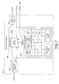
- Referring to FIG. 1, a block diagram of
device 100 is shown in accordance with a preferred embodiment of the present invention. Thedevice 100 may be implemented as an infrared (IR) remote control receiver configured to receive a signal (e.g., REC). Thedevice 100 generally comprises asensor 102, areceiver circuit 104 and aclock circuit 106. - The
sensor 102 may have aninput 108 to receive the signal REC. Anoutput 110 of thesensor 102 may be coupled to aninput 112 of thereceiver circuit 104 to transfer a signal (e.g., PULSE). Thereceiver circuit 104 may have anoutput 114 to present a signal (e.g., INSTR). Thereceiver 104 may have anotheroutput 116 to present another signal (e.g., STATUS). Aninput 118 of thereceiver circuit 104 may be coupled to anoutput 120 of theclock circuit 106 to receive a signal (e.g., CURRENT_TIME). - The signal REC may be implemented as an optical signal. In one embodiment, the optical signal REC may be implemented as an infrared (IR) optical signal. The optical signal REC may transfer codes or instructions from a
remote control 122 to thedevice 100. The instructions may provide parameters for the operation of thedevice 100. The instructions may be pulse encoded within the optical signal REC. The optical signal REC may be implemented as other types of signals, for example radio-frequency, acoustic and electrical, to meet the design criteria of a particular application. - The signal PULSE may be implemented as an electrical signal. The electrical signal PULSE may be an electrical version of the optical signal REC. The electrical signal PULSE may transfer the same instruction carried by the optical signal REC. The instructions may be pulse encoded within the electrical signal PULSE.
- The signal INSTR may be implemented as a decoded instruction signal. The signal INSTR may carry the instructions decoded from the signal PULSE. A unique value may be used to identify each type of instruction presented by the signal INSTR.
- The signal STATUS may be implemented as a status signal. The signal STATUS may provide additional information about the signal INSTR. A valid state may be provided in the signal STATUS while the signal INSTR contains a valid or accepted instruction. An invalid state may be provided in the signal STATUS while the signal INSTR contains an invalid or rejected instruction. In one embodiment, the invalid state information may be presented in the signal INSTR as a special code while all other codes are presumed to be valid. In another embodiment, the signal INSTR may be suppressed by the
receiver circuit 104 while the signal STATUS simultaneously conveys the invalid state. - The signal CURRENT_TIME may be implemented as a time signal. The signal CURRENT_TIME may provide a time value to the
receiver circuit 104 that updates on a periodic basis. The length of a period is generally less than a time duration for receiving an instruction within the signal REC. - The
sensor 102 may be operational to convert the signal REC to the signal PULSE. Different types ofsensors 102 may be implemented to match the type (e.g., optical, radio-frequency, etc.) of signal REC. Thereceiver circuit 104 may be operational to accept or reject instructions within the signal PULSE based upon (i) the type of instruction received, (ii) a previously received instructions, (iii) a time of reception as determined by the signal CURRENT_TIME, and/or (iv) a value of a disable signal allocated to each type of instruction. Theclock circuit 106 may be configured to generate the signal CURRENT_TIME. - The instructions conveyed by the signals REC, PULSE and INSTR may be generally categorized as repeat instructions and non-repeat instructions. A unique non-repeat instruction is generally generated and transmitted by the
remove control 122 for each key press detected by theremote control 122. Examples of non-repeat instructions may include, but are not limited to, volume increase, volume decrease, channel increase, channel decrease, 0, 1, 2, 3, 4, 5, 6, 7, 8, 9, 0, play, stop, fast forward, reverse, pause, record and the like. Repeat instructions generally depend on a previously received non-repeat instruction. One or more repeat instructions may follow any non-repeat instruction while a selected key of theremote control circuit 122 remains pressed. Thedevice 100 may interpret each received repeat instruction as if a duplicate of a last received non-repeat instruction had been received. For example, a volume increase instruction followed by five repeat instructions may be treated as six consecutive volume increase instructions. - Referring to FIG. 2, an
example waveform 124 of the signal REC is shown. Thewaveform 124 generally comprises a non-repeat instruction (e.g., New Key 126) followed by two repeat instructions (e.g.,Repeat Key press 128 and Repeat Key press 130). - Each instruction generally has a constant pulse period or
frame period 131. For example, theframe period 131 may be approximately 108 milliseconds (ms) regardless of the type of instruction being transmitted. Sequential frames may be transmitted without an inter-frame gap. Therefore, a frame for the repeatkey press 130 may be being at a known time (e.g., 216 ms) after a beginning of the frame for thenew key 126. Other implementations of thewaveform 124 may be provided to meet the design criteria of a particular application. - The
new key 126 instruction generally comprises aleader code 132 a followed by aninformation code 134. A combined duration of theleader code 132 a and theinformation code 134 may vary in time depending on the instruction being send. For example, the combined duration may vary from approximately 58.5 ms to approximately 76.5 ms. The remainder of the frame period may be silent. - The repeat
key press 128 instruction generally comprises aleader code 132 b followed by arepeat code 136. A combined duration of theleader code 132 b and therepeat code 136 may be a predetermined time. For example, the predetermined time may be approximately 11.81 ms. The remainder of the frame period may be silent. The repeatkey press 130 instruction may be a copy of the repeatkey press 128. - Referring to FIG. 3, a
waveform 138 of a portion of the newkey press 126 is shown. Thewaveform 138 generally comprises theleader code 132 a, twocustom codes data codes synchronization pulse 148 having a duration and agap 150 having another duration. As an example, the duration of thesynchronization pulse 148 may be approximately 9 ms and the duration of thegap 150 may be approximately 4.5 ms. Thecustom codes data codes waveforms 138 may be implemented for the non-repeat instructions to meet the design criteria of a particular application. - Referring to FIG. 4, a detailed portion of the
waveform 138 is shown. Thecustom code 140 may convey a sequence of logical ones (e.g., “1”) and logical zeros (e.g., “0”) based upon a pulse period modulation. For example, thecode pulse 152 a may define a beginning of a logical zero. In thecode pulse 152 a example, the logical zero may have a duration of approximately 1.125 ms from a start of a current code pulse (e.g., 152 a) until a start of a subsequent code pulse (e.g., 152 b). In contrast, thecode pulse 152 b may define a beginning of a logical one. For example, the logical one may have a period of approximately 2.25 ms from a start of a current code pulse (e.g., 152 b) until a start of a subsequent code pulse (e.g., 152 c). Each of the individual code pulses 152 a-n (and 154 a-m) may have a predetermined period. For example, each code pulse period may be approximately 0.56 ms. - Referring to FIG. 5, a
waveform 156 of the repeatkey press 128 is shown. The repeatkey press 128 generally comprises theleader code 132 b, agap 158 and arepeat code 136. Theleader code 132 b may have a fixed duration. For example, the fixed duration of theleader code 132 b may be approximately 9 ms. Thegap 158 may have another fixed duration. For example, the fixed duration of thegap 158 may be approximately 2.25 ms. Therepeat pulse 136 may have another duration. For example, the duration of therepeat pulse 136 may be approximately 0.56 ms. - Referring to FIG. 6, a
waveform 160 of a carrier is shown. The carrier may be used to build up the synchronization pulses, repeat pulses and code pulses. The carrier generally comprises a sequence ofhigh symbols 162 separated bylow symbols 162. Eachhigh symbol 162 may have a predetermined duration or period. Eachlow symbol 164 may have another predetermined duration or period. For example, the predetermined duration of eachhigh symbol 162 may be approximately 8.77 microseconds (us) and the predetermined duration of eachlow symbol 164 may be approximately 17.53 us for a total period of approximately 26.3 us. A string ofhigh symbols 162 andlow symbols 164 may span a range of time For example, the sting ofhigh symbols 162 andlow symbols 164 may range from approximately 0.56 ms to approximately 9 ms. Thehigh symbols 162 may be implemented as a presence of photons. Thelow symbols 164 may be implemented as an absence at photons. Other types of symbols may be implemented to meet the design criteria of a particular application. - Referring again to FIG. 2, the signal CURRENT_TIME is shown with respect to the
waveform 124. The signal CURRENT_TIME may quantize continuous time into finite periods 165 a-l. Each of the finite periods Tx may have a predetermined period controlled by theclock generator 106. Each of the finite periods 165 may have a unique value (e.g., Tx, where x=n, n+1, n+2, . . . ). The values Tx may increment as time increases. The periods 165 may be non-synchronous or synchronous with the signals REC and PULSE. The periods 165 may be an integer or non-integer traction of theframe period 131. - The
receiver circuit 104 may use the time Tx of the signal CURRENT_TIME to determine when thenew key 126 instruction arrives (e.g., Ta). From the arrival time Ta, thereceiver circuit 104 may determine a validity of the subsequent repeatkey press 128 that may arrive at a later time (e.g., Tb). - For example, the arrival time Ta of the
new key 126 instruction may be detected during theperiod 165 a of the signal CURRENT_TIME. Thereceiver circuit 104 may use the value Tn of theperiod 165 a to calculate a maximum delay in which a valid repeat key instruction may arrive. Likewise, thereceiver circuit 104 may use the value Tn to calculate a minimum delay during which the valid repeat key instruction should not arrive. In one embodiment, the minimum delay and the maximum delay may be a beginning and an end respectively of a finite period 165. In other words, a difference between the minimum delay and the maximum delay may be one finite period 165. For example, the repeatkey press 128 may only be considered valid if the arrival time Tb occurs anywhere within theperiod 165 e at the time Tn+4. - Acceptance of the repeat
key press 128 may cause thereceiver circuit 104 to calculate a new expected arrival time for the repeatkey press 130 based upon the arrival time of the repeatkey press 128. The repeatkey press 130 may be accepted upon arrival after a minimum delay and before a maximum delay after the time Tn+4. As before, the minimum delay (e.g., Tmin) and the maximum delay (e.g., Tmax) may be the beginning and end of a finite period or time, for example the time Tn+8. - Arrival of an instruction may be determined by any one or more features of the instruction. For example, the arrival time may be determined by (i) a start to the leader code 132, (ii) a valid completion of the
synchronization pulse 148, (iii) a valid completion of the leader code 132, (iv) asubsequent pulse 152 or 136 and/or (v) completion of thepulse period 131. Other parameters may be used to define an arrival of an instruction to meet the design criteria of a particular application. - The
receiver circuit 104 may be able to discard a programmable number of repeat key instructions before accepting a subsequent repeat key instruction. The ability to discard some repeat key instructions may allow thereceiver circuit 104 to control a rate at which the prior non-repeat key instruction may be repeated. By way of example, thereceiver circuit 104 may be programmed to discard the repeatkey press 128 after acceptance of the newkey press 126. Therefore, thereceiver circuit 104 may accept the second repeatkey press 130 if the repeatkey press 130 arrives after a minimal delay and before a maximum delay from acceptance of the newkey press 126. For example, thereceiver circuit 104 may be programmed to accept a repeat key instruction that arrives a single discard period after the initial time Tn. As shown in FIG. 2, a discard period may be approximately four finite periods 165 long. Thus, the window to accept the second repeatkey press 130 may anywhere during the finite time Tn+8. - The
receiver circuit 104 may be programmable to ignore all repeat key instructions for certain new key instructions. Thereceiver circuit 104 may contain a signal (e.g., ENABLE_REP) for each type of new key instruction. Upon reception of each new key instruction, thereceiver circuit 104 may check the signal ENABLE_REP, indexed for the received new key instruction, to determine if following repeat key instructions are to be accepted or rejected. - Referring to FIG. 7, a block diagram of the
receiver circuit 104 is shown. Thereceiver circuit 104 generally comprises aninstruction detector circuit 166, atiming circuit 168 and agate circuit 170. Theinstruction detector circuit 166 may receive the signal PULSE from thesensor 102. Theinstruction detector circuit 166 may generate and present a signal (e.g., IN) to thetiming circuit 168. Theinstruction detector circuit 166 may generate and present another signal (e.g., BET) to thetiming circuit 168. Thetiming circuit 168 may generate and present a signal (e.g., OUT) to thegate circuit 170. Thetiming circuit 168 may also generate and present the signal STATUS external to thereceiver circuit 104 and to thegate circuit 170. Thetiming circuit 168 may receive the signal CURRENT TIME from theclock circuit 106. - The signal IN may be implemented as an internal instruction input signal. The signal IN may carry the instructions received by the
sensor 102 and detected by theinstruction detector circuit 166. The signal DET may be implemented as a detection flag. The signal DET may identify when the signal IN contains a valid instruction or code. The signal OUT may be implemented as an internal instruction output signal. The signal OUT may convey a validly received key instruction. In one embodiment, the signal OUT may be suppressed by thegate circuit 170 when an improperly timed repeat key instruction has been received. In another embodiment, the signal OUT may convey an invalid value upon receipt of an illegal or improperly timed instruction. In still another embodiment, thetiming circuit 168 may not present the signal OUT upon receipt of an illegal or improperly timed instruction. - The
instruction detector circuit 166 may examine the signal PULSE to search for valid instructions. Upon receipt of a valid instruction, theinstruction detector circuit 166 may present the valid instruction in the signal IN and set the signal DET to a valid state. Upon receipt of an invalid or partial instruction, theinstruction detector circuit 166 may (i) suppress the invalid instruction or (ii) simultaneously present the invalid instruction in the signal IN and set the signal DET to an invalid state. - The
timing circuit 168 may check for enabled repetition of the most recently received new key instruction. Thetiming circuit 168 may also check the timing of the repeat key instructions against the arrival time of the most recent new key instruction. The method implemented by thetiming circuit 168 may be express by the following pseudo-code:if (NEW_KEY)/ { use new_key; /* store new key */ PREV_DATA_CODE = NEW_KEY; /* store expected time of a repeat key instruction at NEW_T1 */ CODE [NEW_KEY] [NEW_T1] = CURRENT_TIME + CODE [PREV_DATA_CODE] [NUM_DISC_PERIOD] * PULSE_PERIOD; } if (REP_KEY) { /* Check for arrival time and enabled repetition */ if( (CURRENT_TIME == CODE [PREV_DATA_CODE] [NEW_T1]) && CODE [PREV_DATA_CODE] [ENABLE_REP] ) { /* repeat key instruction arrived in calculated window */ use prev_data_code; CODE [PREV_DATA_CODE] [NEW_T1] = CURRENT_TIME + CODE [PREV_DATA_CODE] [NUM_DISC_PERIOD] * PULSE_PERIOD; } else /* repeat key instruction arrived outside calculated window */ do not update timing; } - The
gate circuit 170 may be optionally implemented to pass valid instructions and reject invalid instructions. Thegate circuit 170 may pass the instructions in the signal OUT through to the signal INSTR while the signal STATUS has the valid state. Thegate circuit 170 may suppress the instructions in the signal OUT while the signal STATUS has the invalid state. - The
timing circuit 168 generally comprises alogic circuit 172 and amemory 174. Thelogic circuit 172 generally performs the operations of accepting or rejecting repeat key instructions based upon the signal ENABLE_REP and/or the arrival time. Thelogic circuit 172 may also store the most recently received non-repeat key instruction in thememory 174 and calculate the next valid arrival time of a repeat key instruction. - The
memory 174 generally comprises a lookup table (e.g., CODE [y,x]), a variable (e.g., PREV_DATA_CODE) for the previously received non-repeat key instruction, and a variable (e.g., PULSE_PERIOD) for a duration of an instruction in units of the finite period 165. The parameter y of the lookup table CODE may provide an index for a particular non-repeat key instruction. The parameter x of the lookup table CODE may provide an index for the variables ENABLE_REP, NUM_DISC_PERIOD and NEW_T1. - The main idea is generally that once a new key instruction has been received (e.g., at a time Tx), a first repeat key instruction should be received as defined in
equation 1 as follows: - NEW — T1=Tx+(NUM — DISC — PERIOD*PULSE PERIOD) Eq. (1)
- Reception of the repeat key instruction before or after the time NEW_T1 generally indicates that the repeat key instruction may not be related to the previously received new key instruction, so the repeat key instruction should not be executed. The
clock circuit 106 may use operating system clock ticks as a way to keep track of the time passing from one reception to the other. The lookup table CODE may be set in thememory 174 together with the previously received valid data instruction. Another field may also be added in the lookup table CODE that, for each key instruction, may give a new data code value thus allowing a mapping of protocol defined keys to custom defined keys. The lookup table CODE may be loaded into thememory 174 permanently or at a run time for thetiming circuit 168. - Referring to FIG. 8, a flow diagram for a method of operating the
device 100 is shown. The method generally starts with a reception of the optical signal REC by the sensor 102 (e.g., block 176). Theinstruction detector circuit 166 may generate and present the signal IN with the appropriate instruction code received and assert the signal DET accordingly (e.g., block 178). Thelogic circuit 172 may determine and buffer the arrival time of the instruction as determined by the signal CURRENT_TIME (e.g., block 180). For a non-repeat key instruction type (e.g., the NEW branch from decision block 182)1 thenlogic circuit 172 may store the new instruction in thememory 174 as the variable PREV_DATA_CODE in place of a previous new instruction (e.g., block 184). Thelogic circuit 172 may then calculate and store (in the memory 174) the expected arrival time NEW_T1 of a repeat key instruction dependent on the new key instruction (e.g., block 186). Thelogic circuit 172 may generate (i) the signal INSTR and (ii) the signal STATUS in the valid state (e.g., block 188). - For a repeat key instruction (e.g., the REPEAT branch of decision block 182), the
logic circuit 172 may read the expected arrival time NEW_T1 and the enable flag ENABLE_REP from the memory 174 (e.g., block 190). If the enable flag ENABLE_REP has a disabled state (e.g., the DISABLE branch of the decision block 192), thelogic circuit 172 may generate and present the signal STATUS having the invalid state (e.g., block 194). If the signal ENABLE_REP has an enabled state (e.g., the ENABLE branch of decision block 192), the arrival time of the repeat key instruction may be checked (e.g., decision block 196). For an arrival time greater than the maximum delay (e.g., the YES branch of decision block 196), the logic block may generate the signal STATUS with the invalid state (e.g., block 194) as the repeat key instruction may have arrived too late. - For an arrival time less than or equal to the maximum delay (e.g., the NO branch of decision block 196), the arrival time may be compared against the minimum delay determined by the variables NUM_DISC_PERIOD and PULSE_PERIOD (e.g., decision block 198). For an arrival time less than the minimum delay (e.g., the YES branch of decision block 198), the
logic circuit 172 may generate the signal STATUS with the invalid state (e.g., block 194) as the repeat key instruction may have arrived too early. For an arrival time greater than or equal to the minimum time (e.g., the NO branch of decision block 198), thelogic circuit 172 may recalculate a next expected arrival time NEW_T1 based on the time CURRENT_TIME and store the expected arrival time NEW_T1 in the memory 174 (e.g., block 200). Thelogic circuit 172 may then generate (i) the signal INSTR and (ii) the signal STATUS with the valid state. - The various signals of the present invention are generally “on” (e.g., a digital HIGH, or 1) or “off” (e.g., a digital LOW, or 0). However, the particular polarities of the on (e.g., asserted) and off (e.g., de-asserted) states of the signals may be adjusted (e.g., reversed) accordingly to meet the design criteria of a particular implementation. Additionally, inverters may be added to change a particular polarity of the signals.
- As used herein, the term “simultaneously” is meant to describe events that share some common time period but the term is not meant to be limited to events that begin at the same point in time, end at the same point in time, or have the same duration.
- While the invention has been particularly shown and described with reference to the preferred embodiments thereof, it will be understood by those skilled in the art that various changes in form and details may be made without departing from the spirit and scope of the invention.
Claims (20)
Priority Applications (1)
| Application Number | Priority Date | Filing Date | Title |
|---|---|---|---|
| US10/124,040 US7482944B2 (en) | 2002-04-17 | 2002-04-17 | Method and device for receiving sequential instructions |
Applications Claiming Priority (1)
| Application Number | Priority Date | Filing Date | Title |
|---|---|---|---|
| US10/124,040 US7482944B2 (en) | 2002-04-17 | 2002-04-17 | Method and device for receiving sequential instructions |
Publications (2)
| Publication Number | Publication Date |
|---|---|
| US20030197624A1 true US20030197624A1 (en) | 2003-10-23 |
| US7482944B2 US7482944B2 (en) | 2009-01-27 |
Family
ID=29214525
Family Applications (1)
| Application Number | Title | Priority Date | Filing Date |
|---|---|---|---|
| US10/124,040 Active 2026-11-04 US7482944B2 (en) | 2002-04-17 | 2002-04-17 | Method and device for receiving sequential instructions |
Country Status (1)
| Country | Link |
|---|---|
| US (1) | US7482944B2 (en) |
Cited By (6)
| Publication number | Priority date | Publication date | Assignee | Title |
|---|---|---|---|---|
| US20090091664A1 (en) * | 2007-10-09 | 2009-04-09 | Shahal Shay | Ergonomic learning remote control |
| EP2538692A1 (en) * | 2011-06-23 | 2012-12-26 | Samsung Electronics Co., Ltd. | Device for receiving a remote control signal and a signal processing method thereof |
| CN103685904A (en) * | 2012-09-14 | 2014-03-26 | 华为技术有限公司 | Video camera management method and equipment |
| CN106101790A (en) * | 2016-07-18 | 2016-11-09 | 乐视控股(北京)有限公司 | Signal processing method and device |
| US11350153B2 (en) * | 2020-04-03 | 2022-05-31 | Charter Communications Operating, Llc | Remote control with automated audio and video selection control |
| TWI775137B (en) * | 2020-09-01 | 2022-08-21 | 新唐科技股份有限公司 | Integrated circuit and method of command comparison for infrared receiver |
Families Citing this family (4)
| Publication number | Priority date | Publication date | Assignee | Title |
|---|---|---|---|---|
| US7733425B2 (en) * | 2003-03-31 | 2010-06-08 | Sony Corporation | Automatic picture conditioning based upon user input choosing a video label |
| CN101394406B (en) * | 2008-10-22 | 2012-10-03 | 深圳市金蝶中间件有限公司 | Method and apparatus for preventing duplicate button pressing by user |
| CN105469591A (en) * | 2016-01-04 | 2016-04-06 | 西安交通大学 | Portable infrared remote control pulse signal generator and pulse width correction method |
| CN111260910B (en) * | 2020-02-24 | 2021-08-27 | 珠海荣邦智能科技有限公司 | Control method, device and circuit of infrared transmitting tube |
Citations (6)
| Publication number | Priority date | Publication date | Assignee | Title |
|---|---|---|---|---|
| US4325081A (en) * | 1979-08-10 | 1982-04-13 | Hitachi, Ltd. | Programmed timer for VTR |
| US4866542A (en) * | 1985-12-27 | 1989-09-12 | Sony Corporation | Remote-controlling commander with multi-function rotary dial |
| US5187469A (en) * | 1990-08-06 | 1993-02-16 | Tandy Corporation | Universal remote control including quick touch function |
| US5412377A (en) * | 1990-06-08 | 1995-05-02 | Evans; Benjamin F. | Universal remote control program scheduling system |
| US5677664A (en) * | 1995-10-10 | 1997-10-14 | Jon Snyder, Inc. | Controlling automobile alarm systems |
| US5835665A (en) * | 1997-03-10 | 1998-11-10 | Joseph Enterprises, Inc. | Simplified VCR programmer |
-
2002
- 2002-04-17 US US10/124,040 patent/US7482944B2/en active Active
Patent Citations (6)
| Publication number | Priority date | Publication date | Assignee | Title |
|---|---|---|---|---|
| US4325081A (en) * | 1979-08-10 | 1982-04-13 | Hitachi, Ltd. | Programmed timer for VTR |
| US4866542A (en) * | 1985-12-27 | 1989-09-12 | Sony Corporation | Remote-controlling commander with multi-function rotary dial |
| US5412377A (en) * | 1990-06-08 | 1995-05-02 | Evans; Benjamin F. | Universal remote control program scheduling system |
| US5187469A (en) * | 1990-08-06 | 1993-02-16 | Tandy Corporation | Universal remote control including quick touch function |
| US5677664A (en) * | 1995-10-10 | 1997-10-14 | Jon Snyder, Inc. | Controlling automobile alarm systems |
| US5835665A (en) * | 1997-03-10 | 1998-11-10 | Joseph Enterprises, Inc. | Simplified VCR programmer |
Cited By (11)
| Publication number | Priority date | Publication date | Assignee | Title |
|---|---|---|---|---|
| US20090091664A1 (en) * | 2007-10-09 | 2009-04-09 | Shahal Shay | Ergonomic learning remote control |
| EP2538692A1 (en) * | 2011-06-23 | 2012-12-26 | Samsung Electronics Co., Ltd. | Device for receiving a remote control signal and a signal processing method thereof |
| CN102843530A (en) * | 2011-06-23 | 2012-12-26 | 三星电子株式会社 | Device and signal processing method thereof |
| US9407949B2 (en) | 2011-06-23 | 2016-08-02 | Samsung Electronics Co., Ltd. | Device and signal processing method thereof |
| KR101789225B1 (en) * | 2011-06-23 | 2017-11-20 | 삼성전자주식회사 | Device and signal processing method thereof |
| CN103685904A (en) * | 2012-09-14 | 2014-03-26 | 华为技术有限公司 | Video camera management method and equipment |
| CN106101790A (en) * | 2016-07-18 | 2016-11-09 | 乐视控股(北京)有限公司 | Signal processing method and device |
| US11350153B2 (en) * | 2020-04-03 | 2022-05-31 | Charter Communications Operating, Llc | Remote control with automated audio and video selection control |
| US20220256224A1 (en) * | 2020-04-03 | 2022-08-11 | Charter Communications Operating, Llc | Remote control with automated audio and video selection control |
| US11974003B2 (en) * | 2020-04-03 | 2024-04-30 | Charter Communications Operating, Llc | Remote control with automated audio and video selection control |
| TWI775137B (en) * | 2020-09-01 | 2022-08-21 | 新唐科技股份有限公司 | Integrated circuit and method of command comparison for infrared receiver |
Also Published As
| Publication number | Publication date |
|---|---|
| US7482944B2 (en) | 2009-01-27 |
Similar Documents
| Publication | Publication Date | Title |
|---|---|---|
| US8139653B2 (en) | Multi-channel galvanic isolator utilizing a single transmission channel | |
| EP1110337B1 (en) | Optical remote control interface system and method | |
| US4185273A (en) | Data rate adaptive control device for Manchester code decoders | |
| US4779266A (en) | Encoding and decoding for code division multiple access communication systems | |
| US9118392B2 (en) | Isolated serializer-deserializer | |
| US7482944B2 (en) | Method and device for receiving sequential instructions | |
| JP2621884B2 (en) | Communication method and encoding device | |
| US20020191719A1 (en) | Differential signal-delaying apparatus, receiver employing the apparatus, and communication system | |
| US4779265A (en) | Multiple access communication system | |
| NL8202886A (en) | DEVICE FOR READING DATA USED IN DATA TRANSFER. | |
| US4543611A (en) | Method and an apparatus for image processing | |
| EP0627144B1 (en) | A bit-serial decoder | |
| US5303270A (en) | Frame guard system | |
| SU1695353A1 (en) | Device for receiving excessive signals | |
| SU1145486A1 (en) | Receiver for speed-error minimizing command signals | |
| SU1107336A2 (en) | Vertical synchronization device | |
| RU1805485C (en) | Device for synchronization of cycles | |
| RU2022476C1 (en) | Digital data transmission system characterized by two-sided speed matching | |
| RU2023309C1 (en) | Device for receiving telecontrol programs | |
| JPH05219133A (en) | Coded data reception circuit | |
| JPS5819055A (en) | Clock reproducing circuit | |
| KR940008743B1 (en) | Base decision circuit of Viterbi error correction device | |
| SU1172052A1 (en) | Cycle synchronization device | |
| SU1510105A1 (en) | Data transceiver | |
| SU1753615A1 (en) | Device for transmission of information |
Legal Events
| Date | Code | Title | Description |
|---|---|---|---|
| AS | Assignment |
Owner name: LSI LOGIC CORPORATION, CALIFORNIA Free format text: ASSIGNMENT OF ASSIGNORS INTEREST;ASSIGNOR:BRESIN, GIOVANNI;REEL/FRAME:012840/0568 Effective date: 20020416 |
|
| AS | Assignment |
Owner name: LSI CORPORATION, CALIFORNIA Free format text: MERGER;ASSIGNOR:LSI SUBSIDIARY CORP.;REEL/FRAME:020548/0977 Effective date: 20070404 Owner name: LSI CORPORATION,CALIFORNIA Free format text: MERGER;ASSIGNOR:LSI SUBSIDIARY CORP.;REEL/FRAME:020548/0977 Effective date: 20070404 |
|
| FEPP | Fee payment procedure |
Free format text: PAYOR NUMBER ASSIGNED (ORIGINAL EVENT CODE: ASPN); ENTITY STATUS OF PATENT OWNER: LARGE ENTITY |
|
| STCF | Information on status: patent grant |
Free format text: PATENTED CASE |
|
| FPAY | Fee payment |
Year of fee payment: 4 |
|
| AS | Assignment |
Owner name: DEUTSCHE BANK AG NEW YORK BRANCH, AS COLLATERAL AGENT, NEW YORK Free format text: PATENT SECURITY AGREEMENT;ASSIGNORS:LSI CORPORATION;AGERE SYSTEMS LLC;REEL/FRAME:032856/0031 Effective date: 20140506 Owner name: DEUTSCHE BANK AG NEW YORK BRANCH, AS COLLATERAL AG Free format text: PATENT SECURITY AGREEMENT;ASSIGNORS:LSI CORPORATION;AGERE SYSTEMS LLC;REEL/FRAME:032856/0031 Effective date: 20140506 |
|
| AS | Assignment |
Owner name: LSI CORPORATION, CALIFORNIA Free format text: CHANGE OF NAME;ASSIGNOR:LSI LOGIC CORPORATION;REEL/FRAME:033102/0270 Effective date: 20070406 |
|
| AS | Assignment |
Owner name: AVAGO TECHNOLOGIES GENERAL IP (SINGAPORE) PTE. LTD Free format text: ASSIGNMENT OF ASSIGNORS INTEREST;ASSIGNOR:LSI CORPORATION;REEL/FRAME:035058/0248 Effective date: 20140804 |
|
| AS | Assignment |
Owner name: AGERE SYSTEMS LLC, PENNSYLVANIA Free format text: TERMINATION AND RELEASE OF SECURITY INTEREST IN PATENT RIGHTS (RELEASES RF 032856-0031);ASSIGNOR:DEUTSCHE BANK AG NEW YORK BRANCH, AS COLLATERAL AGENT;REEL/FRAME:037684/0039 Effective date: 20160201 Owner name: LSI CORPORATION, CALIFORNIA Free format text: TERMINATION AND RELEASE OF SECURITY INTEREST IN PATENT RIGHTS (RELEASES RF 032856-0031);ASSIGNOR:DEUTSCHE BANK AG NEW YORK BRANCH, AS COLLATERAL AGENT;REEL/FRAME:037684/0039 Effective date: 20160201 |
|
| AS | Assignment |
Owner name: BANK OF AMERICA, N.A., AS COLLATERAL AGENT, NORTH CAROLINA Free format text: PATENT SECURITY AGREEMENT;ASSIGNOR:AVAGO TECHNOLOGIES GENERAL IP (SINGAPORE) PTE. LTD.;REEL/FRAME:037808/0001 Effective date: 20160201 Owner name: BANK OF AMERICA, N.A., AS COLLATERAL AGENT, NORTH Free format text: PATENT SECURITY AGREEMENT;ASSIGNOR:AVAGO TECHNOLOGIES GENERAL IP (SINGAPORE) PTE. LTD.;REEL/FRAME:037808/0001 Effective date: 20160201 |
|
| FPAY | Fee payment |
Year of fee payment: 8 |
|
| AS | Assignment |
Owner name: AVAGO TECHNOLOGIES GENERAL IP (SINGAPORE) PTE. LTD., SINGAPORE Free format text: TERMINATION AND RELEASE OF SECURITY INTEREST IN PATENTS;ASSIGNOR:BANK OF AMERICA, N.A., AS COLLATERAL AGENT;REEL/FRAME:041710/0001 Effective date: 20170119 Owner name: AVAGO TECHNOLOGIES GENERAL IP (SINGAPORE) PTE. LTD Free format text: TERMINATION AND RELEASE OF SECURITY INTEREST IN PATENTS;ASSIGNOR:BANK OF AMERICA, N.A., AS COLLATERAL AGENT;REEL/FRAME:041710/0001 Effective date: 20170119 |
|
| AS | Assignment |
Owner name: AVAGO TECHNOLOGIES INTERNATIONAL SALES PTE. LIMITED, SINGAPORE Free format text: MERGER;ASSIGNOR:AVAGO TECHNOLOGIES GENERAL IP (SINGAPORE) PTE. LTD.;REEL/FRAME:047195/0827 Effective date: 20180509 Owner name: AVAGO TECHNOLOGIES INTERNATIONAL SALES PTE. LIMITE Free format text: MERGER;ASSIGNOR:AVAGO TECHNOLOGIES GENERAL IP (SINGAPORE) PTE. LTD.;REEL/FRAME:047195/0827 Effective date: 20180509 |
|
| AS | Assignment |
Owner name: AVAGO TECHNOLOGIES INTERNATIONAL SALES PTE. LIMITED, SINGAPORE Free format text: CORRECTIVE ASSIGNMENT TO CORRECT THE EFFECTIVE DATE OF MERGER PREVIOUSLY RECORDED AT REEL: 047195 FRAME: 0827. ASSIGNOR(S) HEREBY CONFIRMS THE MERGER;ASSIGNOR:AVAGO TECHNOLOGIES GENERAL IP (SINGAPORE) PTE. LTD.;REEL/FRAME:047924/0571 Effective date: 20180905 Owner name: AVAGO TECHNOLOGIES INTERNATIONAL SALES PTE. LIMITE Free format text: CORRECTIVE ASSIGNMENT TO CORRECT THE EFFECTIVE DATE OF MERGER PREVIOUSLY RECORDED AT REEL: 047195 FRAME: 0827. ASSIGNOR(S) HEREBY CONFIRMS THE MERGER;ASSIGNOR:AVAGO TECHNOLOGIES GENERAL IP (SINGAPORE) PTE. LTD.;REEL/FRAME:047924/0571 Effective date: 20180905 |
|
| MAFP | Maintenance fee payment |
Free format text: PAYMENT OF MAINTENANCE FEE, 12TH YEAR, LARGE ENTITY (ORIGINAL EVENT CODE: M1553); ENTITY STATUS OF PATENT OWNER: LARGE ENTITY Year of fee payment: 12 |