US20030197469A1 - Plasma display panel and method of manufacturing partitions thereof - Google Patents
Plasma display panel and method of manufacturing partitions thereof Download PDFInfo
- Publication number
- US20030197469A1 US20030197469A1 US10/449,029 US44902903A US2003197469A1 US 20030197469 A1 US20030197469 A1 US 20030197469A1 US 44902903 A US44902903 A US 44902903A US 2003197469 A1 US2003197469 A1 US 2003197469A1
- Authority
- US
- United States
- Prior art keywords
- light emitting
- emitting zone
- filling portion
- display panel
- plasma display
- Prior art date
- Legal status (The legal status is an assumption and is not a legal conclusion. Google has not performed a legal analysis and makes no representation as to the accuracy of the status listed.)
- Granted
Links
Images


Classifications
-
- H—ELECTRICITY
- H01—ELECTRIC ELEMENTS
- H01J—ELECTRIC DISCHARGE TUBES OR DISCHARGE LAMPS
- H01J11/00—Gas-filled discharge tubes with alternating current induction of the discharge, e.g. alternating current plasma display panels [AC-PDP]; Gas-filled discharge tubes without any main electrode inside the vessel; Gas-filled discharge tubes with at least one main electrode outside the vessel
- H01J11/20—Constructional details
- H01J11/34—Vessels, containers or parts thereof, e.g. substrates
- H01J11/36—Spacers, barriers, ribs, partitions or the like
-
- H—ELECTRICITY
- H01—ELECTRIC ELEMENTS
- H01J—ELECTRIC DISCHARGE TUBES OR DISCHARGE LAMPS
- H01J11/00—Gas-filled discharge tubes with alternating current induction of the discharge, e.g. alternating current plasma display panels [AC-PDP]; Gas-filled discharge tubes without any main electrode inside the vessel; Gas-filled discharge tubes with at least one main electrode outside the vessel
- H01J11/10—AC-PDPs with at least one main electrode being out of contact with the plasma
- H01J11/12—AC-PDPs with at least one main electrode being out of contact with the plasma with main electrodes provided on both sides of the discharge space
-
- H—ELECTRICITY
- H01—ELECTRIC ELEMENTS
- H01J—ELECTRIC DISCHARGE TUBES OR DISCHARGE LAMPS
- H01J11/00—Gas-filled discharge tubes with alternating current induction of the discharge, e.g. alternating current plasma display panels [AC-PDP]; Gas-filled discharge tubes without any main electrode inside the vessel; Gas-filled discharge tubes with at least one main electrode outside the vessel
- H01J11/20—Constructional details
- H01J11/48—Sealing, e.g. seals specially adapted for leading-in conductors
-
- H—ELECTRICITY
- H01—ELECTRIC ELEMENTS
- H01J—ELECTRIC DISCHARGE TUBES OR DISCHARGE LAMPS
- H01J11/00—Gas-filled discharge tubes with alternating current induction of the discharge, e.g. alternating current plasma display panels [AC-PDP]; Gas-filled discharge tubes without any main electrode inside the vessel; Gas-filled discharge tubes with at least one main electrode outside the vessel
- H01J11/20—Constructional details
- H01J11/54—Means for exhausting the gas
-
- H—ELECTRICITY
- H01—ELECTRIC ELEMENTS
- H01J—ELECTRIC DISCHARGE TUBES OR DISCHARGE LAMPS
- H01J9/00—Apparatus or processes specially adapted for the manufacture, installation, removal, maintenance of electric discharge tubes, discharge lamps, or parts thereof; Recovery of material from discharge tubes or lamps
- H01J9/24—Manufacture or joining of vessels, leading-in conductors or bases
- H01J9/241—Manufacture or joining of vessels, leading-in conductors or bases the vessel being for a flat panel display
- H01J9/242—Spacers between faceplate and backplate
-
- H—ELECTRICITY
- H01—ELECTRIC ELEMENTS
- H01J—ELECTRIC DISCHARGE TUBES OR DISCHARGE LAMPS
- H01J2211/00—Plasma display panels with alternate current induction of the discharge, e.g. AC-PDPs
- H01J2211/20—Constructional details
- H01J2211/34—Vessels, containers or parts thereof, e.g. substrates
- H01J2211/36—Spacers, barriers, ribs, partitions or the like
- H01J2211/368—Dummy spacers, e.g. in a non display region
Definitions
- the present invention relates to a plasma display panel and a method of manufacturing partitions thereof, and more particularly, to a plasma display panel in which neon light emission due to mis-discharge in a non-light emitting zone is fundamentally removed, and to a method of manufacturing partitions thereof.
- a typical plasma display device for displaying an image by using a gas discharge phenomenon is widely noted for its superior display capabilities (display capacity, brightness, contrast, afterimage, and a viewing angle) so as to replace a CRT.
- discharge is generated between electrodes in a gas by direct current or alternating current applied to the electrodes. Then, a fluorescent substance is excited by an ultraviolet ray radiated as the discharge is generated, and a light is emitted.
- FIG. 1 is an exploded perspective view showing a panel of a typical alternating current type plasma display device.
- a first electrode 13 a which is a transparent display electrode
- a second electrode 13 b which is an address electrode
- the first electrode 13 a includes an X electrode and a Y electrode.
- a sustaining discharge is generated between a pair of the first electrodes 13 a during operation of the panel.
- the first and second electrodes 13 a and 13 b are formed in strips, facing to each other, on the inner surfaces of the front glass substrate 11 and the rear glass substrate 12 , respectively.
- the first and second electrodes 13 a and 13 b cross each other.
- a dielectric layer 14 and a protective layer 15 are stacked in order on the inner surface of the front glass substrate 11 .
- Partitions 17 are formed on the upper surface of a dielectric layer 14 ′ formed on the rear glass substrate 12 .
- a cell 19 is formed by the partitions 17 and is filled with an inert gas such as neon (Ne) and xenon (Xe).
- a fluorescent substance 18 is coated on a predetermined portion of the inside of each cell 19 .
- a bus electrode 13 c is formed on the surface of the first electrode 13 a to prevent line resistance, which increases as the length of the first electrode 13 a increases.
- a high voltage (a trigger voltage) is applied to generate a discharge between the X electrode of the first electrode 13 a and the second electrode 13 b .
- the discharge is generated.
- the trigger voltage exceeds a threshold voltage
- the discharge gas in the cell 19 becomes a plasma state by the discharge.
- a stable discharge state can be maintained between pairs of the first electrodes 13 a (see FIG. 2).
- this sustaining discharge state of the discharge lights generated, light in a range of an ultraviolet area collides with the fluorescent substance 18 and emits another light. Accordingly, each pixel formed by a unit of the cell 19 can display an image.
- FIG. 2 is a sectional view showing the assembled plasma display panel of FIG. 1 by cutting the partitions in a widthwise direction.
- the same reference numerals are used for the same elements shown in FIGS. 1 and 2.
- the front glass substrate 11 and the rear glass substrate 12 are coupled to each other with the partitions 17 interposed therebetween.
- Such coupling is made by a sealing material having similar properties to those of a substrate material such as a frit glass 22 coated between the front and rear glass substrates 11 and 12 .
- the frit glass 22 is coated on the inner surfaces of the front and rear substrates 11 and 12 along the edge thereof.
- the frit glass 22 is heated and melted in a state in which the front and rear substrates 11 and 12 are pressed against each other, and then is solidified so that the substrates 11 and 12 can be combined by being attached to each other.
- An outermost partition 23 is positioned at the edge of the substrates 11 and 12 and defines a non-light emitting zone 21 with the frit glass 22 . That is, the non-light emitting zone 21 is defined between the outermost partition 23 and the frit glass 22 . Since the second electrode 13 b is not formed in the non-light emitting zone 21 , and since the fluorescent substance 18 is not coated thereon, theoretically, no discharge is generated.
- the non-light emitting zone 21 is also called a dummy and margin zone, and is formed at the outskirts of a display where an image is displayed.
- the dummy zone prevents an edge effect that may occur in discharge cells 19 at the outermost area of the display, and the margin zone compensates for a limit in accuracy of the manufacturing processes.
- the dummy and margin zone 21 is designed considering a property of each of the layers of a plasma display panel.
- the non-light emission zone 21 is actually filled with the discharge gas filled in the discharge cell 19 , when the sustaining discharge is generated between a pair of first electrodes 13 a , discharge is generated in the non-light emitting zone 21 .
- Such a mis-discharge phenomenon causes light emission by the discharge gas itself. In particular, a light emission phenomenon of an orange color occurs.
- the overall color purity of a display is lowered due to the presence of the non-light emitting zone 21 .
- a dummy electrode is used in the conventional technology.
- a plurality of dummy electrodes is formed parallel to an address electrode at a portion corresponding to the outermost portion of a display area.
- the dummy electrodes are electrically connected to one another to be connected in common with an external connection terminal.
- a dummy electrode is formed parallel to an address electrode at a portion corresponding to the outermost portion of a display area.
- the outermost address electrode and the dummy electrode are electrically connected to each other.
- a plurality of dummy electrodes is formed parallel to an address electrode at a portion corresponding to the outermost portion of a display area.
- the outermost address electrode and the dummy electrode are electrically connected to each other.
- a predetermined voltage is applied to the outermost address electrode during a priming discharge period, an address discharge period, and a sustain discharge period.
- a plasma display panel comprising a front glass substrate and a rear glass substrate coupled to each other by a sealing material coated at edges of the front and rear glass substrates, first and second electrodes respectively formed to cross each other on opposing inner surfaces of the front and rear glass substrates, a dielectric layer formed on each of the opposing inner surfaces of the front and rear glass substrates to cover the first and second electrodes, respective partitions formed on an upper surface of the dielectric layer of the rear glass substrate; red, green and blue fluorescent substances coated between the partitions, and a non-light emitting zone filling portion formed by filling a non-light emitting zone between an outermost partition among the partitions and the sealing material with a material for the partition.
- the outermost partition and the non-light emitting zone filling portion are substantially formed integrally.
- the non-light emitting zone filling portion completely fills a space between the sealing material and the outermost partition.
- the non-light emitting zone filling portion covers end portions of the first electrodes formed on the front glass substrate.
- a gas exhaust hole is formed at an upper surface of the non-light emitting zone filling portion parallel to a lengthwise direction of the partition.
- a depth of the gas exhaust hole is within a range of 10 ⁇ m through 160 ⁇ m.
- a plasma display panel comprising a front glass substrate and a rear glass substrate coupled to each other by a sealing material coated at the edges of both substrates, first and second electrodes respectively formed to cross each other on opposing inner surfaces of the front and rear glass substrates, a dielectric layer formed on each of the opposing inner surfaces of the front and rear glass substrates to cover the first and second electrodes, partitions formed on an upper surface of the dielectric layer of the rear glass substrate, red, green and blue fluorescent substances coated between the respective partitions, and a non-light emitting zone filling portion formed by filling a non-light emitting zone between an outermost partition among the partitions and the sealing material to be close to the outermost partition using the material for the partition, thereby forming an empty space between the sealing material and the non-light emitting zone filling portion and covering end portions of the electrodes formed on the front glass substrate.
- a width of the non-light emitting zone filling portion is equal to a length of end portions of the first electrodes on the front glass substrate which extend past the outermost partition.
- the width of the non-light emitting zone filling portion is greater than a length of end portions of the first electrodes on the front glass substrate which extend past the outermost partition.
- the sum (W3) of a width of the non-light emitting zone filling portion and a width of the outermost partition is 1.0 mm, and a length of the end portion of each of the first electrodes on the front glass substrate covered by the non-light emitting zone filling portion and the outermost partition is 0.3 mm.
- the first electrodes on the front glass substrate extend past the non-light emitting zone filling portion under the condition that the width of the empty space is less than 50 ⁇ m.
- a method of manufacturing partitions of a plasma display panel comprising coating a material for partitions on the upper surface of a dielectric layer on a glass substrate also having electrodes in a predetermined pattern so as to form a cured pattern of dry film resist to shield the partitions and portions corresponding to a non-light emitting zone between an outermost partition and a sealing material by coating a dry film resist on the upper surface of the coated partition material, exposing the dry film resist, and developing the exposed dry film resist, and partially removing the partition material by ejecting abrasion particles at a high speed using the cured pattern as a mask.
- FIG. 1 is an exploded perspective view of a conventional plasma display panel
- FIG. 2 is a sectional view of the conventional plasma display panel of FIG. 1;
- FIG. 3 is a sectional view showing a plasma display panel according to an embodiment of the present invention.
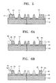
- FIGS. 4A through 4E are sectional views showing a method of manufacturing partitions of the plasma display panel of FIG. 3 according to an embodiment of the present invention
- FIG. 5 is a sectional view showing the structure of a rear glass substrate of a plasma display panel according to another embodiment of the present invention.
- FIG. 6A and FIG. 7 are a sectional view of the rear glass substrate and a bottom view of a front glass substrate of the plasma display panel according to another embodiment of the present invention.
- FIG. 6B is a sectional view of a rear glass substrate of a plasma display panel according to yet another embodiment of the present invention.
- FIG. 8 is a view showing a plasma display panel according to still yet another embodiment of the present invention corresponding to a circled portion of FIG. 7 indicated by reference character A.
- FIG. 3 shows a cross section in a widthwise direction across partitions 17 of a plasma display panel according to an embodiment of the present invention.
- the same elements as the plasma display panel of FIG. 2 are indicated by the same reference numerals.
- the first electrode 13 a , a third electrode (not shown), the dielectric layer 14 , and the protective layer 15 are formed in order on the front glass substrate 11 .
- the second electrode 13 b , the dielectric layer 14 ′, and the partitions 17 are formed in order on the rear glass substrate 12 .
- the front and rear glass substrates 11 and 12 are combined with each other by a sealing material such as the frit glass 22 .
- the frit glass 22 is coated on the inner surfaces of the front and rear glass substrates 11 and 12 along the edge thereof, as described above.
- the frit glass 22 is heated to a melting point and solidified so that the substrates 11 and 12 can be combined by being attached to each other.
- a non-light emitting zone filling portion 31 is formed integrally with the outermost partitions 33 in the non-light emitting zone (shown as element 21 in FIG. 2) formed between the outermost partition and the frit glass 22 .
- the non-light emitting zone filling portion 31 completely fills the space in the non-light emitting zone 21 to prevent the non-light emitting zone 21 from being filled with a discharge gas. That is, as can be seen from FIG.
- the non-light emitting zone filling portion 31 is formed by filling the non-light emitting zone 21 defined between the outermost partition 33 and the frit glass 22 (as indicated by a dotted line) with the same material as used for the partitions 33 , where the non-light emitting zone filling portion 31 having the same height as the partitions 33 .
- the non-light emitting zone filling portion 31 can be understood as one being formed by extending the outermost partition 33 to the inner surface of the frit glass 22 . However, it is understood that the non-light emitting zone filling portion 31 could also be separately manufactured and inserted into the non-light emitting zone 21 .
- the mis-discharge is not generated in the non-light emitting zone 21 in the panel having the structure shown in FIG. 3 both because there is no space to be filled with the discharge gas, and because the end portions of the electrodes 13 a formed on the front glass substrate 11 are covered by the non-light emitting zone filling portion 31 . That is, the end portions of the X electrode or the Y electrode of the electrodes 13 a formed on the front glass substrate 11 are typically extended lengthwise to end between the frit glass 22 and the outermost partition 33 . Since the non-light emission zone filling portion 31 covers the end portions of the first electrodes 13 a , mis-discharge is not generated. This mechanism will be later described in detail with reference to FIG. 7.
- FIG. 4A shows a method of manufacturing partitions of the plasma display panel described above according to an embodiment of the present invention.
- the rear glass substrate 12 is provided.
- the rear glass substrate has the second electrode 13 b (an address electrode) and the dielectric layer 14 ′ are formed on the rear glass substrate 12 using a conventional method.
- a partition material 41 is coated on the entire upper surface of the dielectric layer 14 ′.
- FIG. 4C shows that a dry film resist (DFR) is coated on the surface of the partition material 41 to form a DFR layer 42 .
- the DFR layer 42 is formed on the entire surface of the partition material 41 .
- DFR dry film resist
- the DFR layer 42 is formed to have a predetermined pattern 42 ′, and the partition material 41 is removed by a sand blasting method to have a predetermined pattern.
- the DFR layer 42 is formed to have a predetermined cured pattern 42 ′ as shown in FIG. 4D using an exposure and developing processes. That is, the DFR layer 42 is partially cured by the exposure process, and developed so that the cured pattern 42 ′ remains. As shown, in a portion corresponding to the upper portion of the non-light emitting zone 21 shown in FIG. 2, the DFR layer 42 remains in a pattern 43 ′.
- the cured patterns 42 ′ and 43 ′ of the DFR layer 42 serve as masks with respect to abrasion particles 47 ejected at a high speed. Thus, a portion of the partition material 41 not shielded by the cured patterns 42 ′ and 43 ′ is removed by the abrasion particles 47 using sand blasting.
- FIG. 4E shows the completed partitions 17 and 33 .
- the cured patterns 42 ′ and 43 ′ are removed after the partitions 17 and 33 are completely formed by the sand blasting method.
- the outermost partition 33 is located at the outermost position. As shown, substantially, the outermost partition 33 and the non-light emitting zone filling portion 31 are integrally formed.
- Reference numeral 45 ′ denotes a space where the frit glass 22 shown in FIG. 3 is coated.
- FIGS. 4A through 4E Although the method of manufacturing partitions of a plasma display panel using a sand blasting method is shown in FIGS. 4A through 4E, it is obvious that other methods can be adopted to form the non-light emitting zone filling portion 31 using the partition material 41 in the non-light emitting zone 21 shown in FIG. 2.
- the partitions 17 and 33 are formed by a printing method
- the partition material 41 is printed onto the non-light emitting zone 21 of FIG. 2 so that a plasma display panel of the present invention can be manufactured.
- the partition material 41 can be printed onto the non-light emitting zone 21 of FIG. 2 by appropriately changing a screen used in the method.
- FIG. 5 shows the structure of a rear glass substrate of a plasma display panel according to another embodiment of the present invention.
- the basic structure is similar to the structure described above and the same elements are indicated by the same reference numerals.
- a non-light emitting zone filling portion 51 is formed between the outermost partition 23 and the frit glass space 45 ′, and a gas exhaust hole 52 is formed at an upper surface of the non-light emitting zone filling portion 51 .
- end portions of the X electrode and the Y electrode of the electrode 13 a formed on the front glass substrate are partially covered by the non-light emitting zone filling portion 51 having the gas exhaust hole 52 .
- the gas exhaust hole 52 facilitates the exhaustion of gas from inside the panel.
- the gas exhaust hole 52 extends in a lengthwise direction parallel to the partitions 17 .
- the depth and width of the gas exhaust hole 52 may be variously formed so that mis-discharge is not generated.
- the gas exhaust hole 52 is formed too deep, the amount of a discharge gas filled therein is large.
- the width of the gas exhaust hole 52 is formed too wide, the length of an end portion of an electrode exposed in the gas exhaust hole 52 is extended.
- the height of the partition 17 is 160 ⁇ m high, the depth of the gas exhaust hole 52 is preferably within a range of 10 ⁇ m through 160 ⁇ m.
- the width of one gas exhaust hole 52 is preferably less than 300 ⁇ m.
- FIGS. 6A and 7 are sectional views of a rear glass substrate and a bottom surface of a front glass substrate of a plasma display panel according to yet another embodiment of the present invention.
- the structure shown in FIG. 6A is similar to the structure of the plasma display panel described above. The same elements are indicated by the same reference numerals.
- a non-light emitting zone filling portion 61 is formed in a non-light emitting zone 21 shown in FIG. 2 formed between the outermost partition 23 and the frit glass space 45 ′.
- the non-light emitting zone filling portion 61 does not fill the entire space of the non-light emitting zone 21 , but partially fills only a portion closest to the outermost partition 23 .
- An empty space 62 is formed between the non-light emitting zone filling portion 61 and the frit glass space 45 ′.
- the empty space 62 facilitates the exhaustion and injection of gas.
- the interval between the outermost partition 23 and the frit glass space 45 ′ is 20 mm, and the width of the non-light emitting zone filling portion 61 is less than 10 mm. That is, about half the non-light emitting zone 21 of FIG. 2 between the outermost partition 23 and the frit glass space 45 ′ is filled with the non-light emitting zone filling portion 61 , and the remaining empty space 62 is used for exhaustion of gas.
- the non-light emitting zone filling portion 61 should be formed such that it can cover each of the end portions of the X electrode 73 a and the Y electrode 73 b to be formed on the front glass substrate. That is, as shown in FIG. 7, the X electrode 73 a and Y electrode 73 b are formed in pairs parallel to each other on the front glass substrate 11 .
- One end portion of each of the electrodes 73 a , 73 b is a terminal connected to an external circuit that starts at the edge of the front glass substrate 11 .
- the other end portion ends at a position corresponding to the space between the outermost partition 23 and the frit glass space 45 ′.
- terminals of X electrodes 73 a are formed at the left edge of the front glass substrate 11 while terminals of Y electrodes 73 b are formed at the right edge of the front glass substrate 11 .
- the other end portion of the X electrode 73 a which is not a terminal, ends at a position corresponding to the space between the outermost partition 23 and the frit glass space 45 ′ at the right side of the substrate
- the other end portion of the Y electrode 73 b which is not a terminal, ends at a position corresponding to the space between the outermost partition 23 and the frit glass space 45 ′ at the left side of the substrate.
- the non-light emitting zone filling portion 61 consequently covers all the end portions of the electrodes 73 a and 77 b disposed between a portion 75 where frit glass (not shown) is coated and the positions 77 a and 77 b corresponding to the outermost partitions 23 .
- the above structure can prevent mis-discharge between the electrodes located between the frit glass coating position 75 and a position 77 where the partitions are formed.
- mis-discharge can also be prevented without having the outermost partition 23 and the non-light emitting zone filling portion 61 be of the same height. For instance, if the height difference is less than 20 ⁇ m, mis-discharge is prevented where the width of the empty space 62 is less than 50 ⁇ m. Even if the width of the empty space 62 is not less than 50 ⁇ m, the probability of mis-discharge is low.
- mis-discharge between the electrodes 73 a and 73 b can be prevented under a predetermined condition. That is, when the end portions, which are not the terminals for external connection of the X or Y electrodes 73 a and 73 b , are not completely covered by the non-light emitting zone filling portion 61 , and are extended above the empty space 62 past the non-light emitting zone filling portion 61 , mis-discharge is not generated if the width of the empty space 62 is less than 50 ⁇ m.
- FIG. 6B shows a plasma display panel according to still yet another embodiment of the present invention.
- This embodiment may be understood as one combining the embodiments shown in FIGS. 5 and 6A.
- a non-light emitting zone filling portion 63 is formed closer to the outermost partition 23 , so that an empty space 62 is formed between the non-light emitting zone filling portion 63 and the frit glass space 45 ′.
- a gas exhaust hole 64 is formed at an upper surface of the non-light emitting zone filling portion 63 .
- the gas exhaust hole 64 extends in a lengthwise direction of the partition, and may be formed in multiple numbers and parallel to one another.
- the non-light emitting zone filling portion 63 where the gas exhaust hole 64 is formed covers the end portion of the electrode 13 a (not shown).
- FIG. 8 is a view showing a plasma display panel according to still yet another embodiment of the present invention, corresponding to a circled portion of FIG. 7 indicated by reference letter A.
- the overall structure of the plasma display panel shown in FIG. 8 is similar to that of the plasma display panel shown in FIG. 7, and the same elements are indicated by the same reference numerals.
- End portions of the X and Y electrodes 81 and 82 formed on the front glass substrate 11 are extended to cross a part of the width of a non-light emitting zone filling portion 61 ′.
- the non-light emitting zone filling portion 61 of FIG. 6A formed at each of the left and right sides of the front glass substrate 11 is indicated by reference numeral 61 ′ in FIG. 8, and the outer most partition 23 of FIG. 6A is indicated by reference numeral 79 .
- An area 83 corresponds to a length of an extended end portion of the electrode 81 from the outermost partition 79 into the non-light emitting zone filling portion 61 ′.
- W1 denotes a width of the outermost partition 79
- W2 denotes a length of the electrode 81 extending above the upper surface of the outermost partition 79
- W3 denotes the sum of the width W1 and a width of the non-light emitting zone filling portion 61 ′.
- the non-light emitting zone filling portion 61 ′ is an area corresponding to the width of W3 excluding W1.
- W1 is about 0.1 mm and W3 is about 1.0 mm.
- the area 83 is about 0.2 mm.
- W2 which is the length of an end portion of the electrode 81 covered by the outermost partition 79 and the non-light emitting zone filling portion 61 ′ corresponds to about 0.3 mm. That is, in the embodiment shown in FIG. 7, the end portions of the electrodes 73 a and 73 b extend throughout the entire width of the non-light emitting zone filling portion 61 ′ while, in the embodiment shown in FIG. 8, the end portion of the electrode 81 extends over a part of the width of the non-light emitting zone filling portion 61 ′.
- the length of the extended end portion of the electrodes covered by the non-light emitting zone filling portion 61 ′ and the outermost partition 79 is about 0.3 mm as described above. In the embodiment shown in FIG. 8, even when the end portions of the electrodes 81 and 82 are extended as the substrate is contracted or expanded, they do not protrude from the non-light emitting zone filling portion 61 ′ into the empty space 62 .
- the end portions of the electrodes are covered by the non-light emitting zone filling portion, mis-discharge caused by mis-alignment of the substrates and an undesired positioning of an end portion of the electrode in a discharge cell as the substrate contracts or expands due to thermal deformation can be prevented. That is, by completely covering the end portion of the electrode with the non-light emitting zone filling portion, if dispersion of process occurs, mis-discharge is prevented since no discharge space is present.
- the non-light emitting zone is filled with a material used for the partition, intrusion of a discharge gas thereto is fundamentally prevented. Thus, lowering of color purity due to mis-discharge can be prevented.
Landscapes
- Engineering & Computer Science (AREA)
- Physics & Mathematics (AREA)
- Plasma & Fusion (AREA)
- Manufacturing & Machinery (AREA)
- Gas-Filled Discharge Tubes (AREA)
Abstract
Description
- This application is a continuation of U.S. patent application Ser. No. 09/840,290, filed Apr. 24, 2001 and currently pending, which claims the benefit of Korean Application Nos. 00-62873 and 00-21645, filed respectively on Oct. 25, 2000 and Apr. 24, 2000, in the Korean Industrial Property Office, the disclosures of which are incorporated herein by reference.
- 1. Field of the Invention
- The present invention relates to a plasma display panel and a method of manufacturing partitions thereof, and more particularly, to a plasma display panel in which neon light emission due to mis-discharge in a non-light emitting zone is fundamentally removed, and to a method of manufacturing partitions thereof.
- 2. Description of the Related Art
- A typical plasma display device for displaying an image by using a gas discharge phenomenon is widely noted for its superior display capabilities (display capacity, brightness, contrast, afterimage, and a viewing angle) so as to replace a CRT. In the plasma display device, discharge is generated between electrodes in a gas by direct current or alternating current applied to the electrodes. Then, a fluorescent substance is excited by an ultraviolet ray radiated as the discharge is generated, and a light is emitted.
- FIG. 1 is an exploded perspective view showing a panel of a typical alternating current type plasma display device. Referring to the drawing, a
first electrode 13 a, which is a transparent display electrode, and asecond electrode 13 b, which is an address electrode, are formed between afront glass substrate 11 and arear glass substrate 12. Thefirst electrode 13 a includes an X electrode and a Y electrode. A sustaining discharge is generated between a pair of thefirst electrodes 13 a during operation of the panel. The first andsecond electrodes front glass substrate 11 and therear glass substrate 12, respectively. When the front andrear glass substrates second electrodes dielectric layer 14 and aprotective layer 15 are stacked in order on the inner surface of thefront glass substrate 11.Partitions 17 are formed on the upper surface of adielectric layer 14′ formed on therear glass substrate 12. Acell 19 is formed by thepartitions 17 and is filled with an inert gas such as neon (Ne) and xenon (Xe). Afluorescent substance 18 is coated on a predetermined portion of the inside of eachcell 19. Abus electrode 13 c is formed on the surface of thefirst electrode 13 a to prevent line resistance, which increases as the length of thefirst electrode 13 a increases. - In the operation of the plasma display device having the above structure, first, a high voltage (a trigger voltage) is applied to generate a discharge between the X electrode of the
first electrode 13 a and thesecond electrode 13 b. When anions are accumulated in thedielectric layer 14 by the trigger voltage, the discharge is generated. When the trigger voltage exceeds a threshold voltage, the discharge gas in thecell 19 becomes a plasma state by the discharge. Thus, a stable discharge state can be maintained between pairs of thefirst electrodes 13 a (see FIG. 2). In this sustaining discharge state, of the discharge lights generated, light in a range of an ultraviolet area collides with thefluorescent substance 18 and emits another light. Accordingly, each pixel formed by a unit of thecell 19 can display an image. - FIG. 2 is a sectional view showing the assembled plasma display panel of FIG. 1 by cutting the partitions in a widthwise direction. The same reference numerals are used for the same elements shown in FIGS. 1 and 2.
- Referring to the drawing, the
front glass substrate 11 and therear glass substrate 12 are coupled to each other with thepartitions 17 interposed therebetween. Such coupling is made by a sealing material having similar properties to those of a substrate material such as afrit glass 22 coated between the front andrear glass substrates frit glass 22 is coated on the inner surfaces of the front andrear substrates frit glass 22 is heated and melted in a state in which the front andrear substrates substrates - An
outermost partition 23 is positioned at the edge of thesubstrates non-light emitting zone 21 with thefrit glass 22. That is, thenon-light emitting zone 21 is defined between theoutermost partition 23 and thefrit glass 22. Since thesecond electrode 13 b is not formed in thenon-light emitting zone 21, and since thefluorescent substance 18 is not coated thereon, theoretically, no discharge is generated. Thenon-light emitting zone 21 is also called a dummy and margin zone, and is formed at the outskirts of a display where an image is displayed. Within the dummy andmargin zone 21, the dummy zone prevents an edge effect that may occur indischarge cells 19 at the outermost area of the display, and the margin zone compensates for a limit in accuracy of the manufacturing processes. The dummy andmargin zone 21 is designed considering a property of each of the layers of a plasma display panel. However, since thenon-light emission zone 21 is actually filled with the discharge gas filled in thedischarge cell 19, when the sustaining discharge is generated between a pair offirst electrodes 13 a, discharge is generated in thenon-light emitting zone 21. Such a mis-discharge phenomenon causes light emission by the discharge gas itself. In particular, a light emission phenomenon of an orange color occurs. Thus, the overall color purity of a display is lowered due to the presence of thenon-light emitting zone 21. - To prevent such a phenomenon, a dummy electrode is used in the conventional technology. For example, a plurality of dummy electrodes is formed parallel to an address electrode at a portion corresponding to the outermost portion of a display area. The dummy electrodes are electrically connected to one another to be connected in common with an external connection terminal. Also, a dummy electrode is formed parallel to an address electrode at a portion corresponding to the outermost portion of a display area. The outermost address electrode and the dummy electrode are electrically connected to each other. Further, a plurality of dummy electrodes is formed parallel to an address electrode at a portion corresponding to the outermost portion of a display area. The outermost address electrode and the dummy electrode are electrically connected to each other. A predetermined voltage is applied to the outermost address electrode during a priming discharge period, an address discharge period, and a sustain discharge period. However, since the above conventional technologies require an additional dummy electrode, the structures thereof become complicated.
- To solve the above problem, it is an object of the present invention to provide a plasma display panel which can prevent a mis-discharge phenomenon in a non-light emitting zone.
- It is another object of the present invention to provide a method of manufacturing partitions of the plasma display panel to prevent a mis-discharge phenomenon in the non-light emitting zone.
- Additional objects and advantages of the invention will be set forth in part in the description which follows and, in part, will be obvious from the description, or may be learned by practice of the invention.
- Accordingly, to achieve the above and other objects, there is provided a plasma display panel according to an embodiment of the present invention comprising a front glass substrate and a rear glass substrate coupled to each other by a sealing material coated at edges of the front and rear glass substrates, first and second electrodes respectively formed to cross each other on opposing inner surfaces of the front and rear glass substrates, a dielectric layer formed on each of the opposing inner surfaces of the front and rear glass substrates to cover the first and second electrodes, respective partitions formed on an upper surface of the dielectric layer of the rear glass substrate; red, green and blue fluorescent substances coated between the partitions, and a non-light emitting zone filling portion formed by filling a non-light emitting zone between an outermost partition among the partitions and the sealing material with a material for the partition.
- According to an aspect of the present invention, the outermost partition and the non-light emitting zone filling portion are substantially formed integrally.
- According to still another aspect of the present invention, the non-light emitting zone filling portion completely fills a space between the sealing material and the outermost partition.
- According to yet another aspect of the present invention, the non-light emitting zone filling portion covers end portions of the first electrodes formed on the front glass substrate.
- According to a further aspect of the present invention, a gas exhaust hole is formed at an upper surface of the non-light emitting zone filling portion parallel to a lengthwise direction of the partition.
- According to a yet further aspect of the present invention, a depth of the gas exhaust hole is within a range of 10 μm through 160 μm.
- According to another embodiment of the present invention, there is provided a plasma display panel comprising a front glass substrate and a rear glass substrate coupled to each other by a sealing material coated at the edges of both substrates, first and second electrodes respectively formed to cross each other on opposing inner surfaces of the front and rear glass substrates, a dielectric layer formed on each of the opposing inner surfaces of the front and rear glass substrates to cover the first and second electrodes, partitions formed on an upper surface of the dielectric layer of the rear glass substrate, red, green and blue fluorescent substances coated between the respective partitions, and a non-light emitting zone filling portion formed by filling a non-light emitting zone between an outermost partition among the partitions and the sealing material to be close to the outermost partition using the material for the partition, thereby forming an empty space between the sealing material and the non-light emitting zone filling portion and covering end portions of the electrodes formed on the front glass substrate.
- According to still another aspect of the present invention, a width of the non-light emitting zone filling portion is equal to a length of end portions of the first electrodes on the front glass substrate which extend past the outermost partition.
- According to a yet another aspect of the present invention, the width of the non-light emitting zone filling portion is greater than a length of end portions of the first electrodes on the front glass substrate which extend past the outermost partition.
- According to a further aspect of the present invention, the sum (W3) of a width of the non-light emitting zone filling portion and a width of the outermost partition is 1.0 mm, and a length of the end portion of each of the first electrodes on the front glass substrate covered by the non-light emitting zone filling portion and the outermost partition is 0.3 mm.
- According to a yet further aspect of the present invention, the first electrodes on the front glass substrate extend past the non-light emitting zone filling portion under the condition that the width of the empty space is less than 50 μm.
- According to a still further embodiment of the present invention, there is provided a method of manufacturing partitions of a plasma display panel comprising coating a material for partitions on the upper surface of a dielectric layer on a glass substrate also having electrodes in a predetermined pattern so as to form a cured pattern of dry film resist to shield the partitions and portions corresponding to a non-light emitting zone between an outermost partition and a sealing material by coating a dry film resist on the upper surface of the coated partition material, exposing the dry film resist, and developing the exposed dry film resist, and partially removing the partition material by ejecting abrasion particles at a high speed using the cured pattern as a mask.
- The above and other objects and advantages of the present invention will become more apparent and more readily appreciated from the following description of the preferred embodiments thereof with reference to the attached drawings in which:
- FIG. 1 is an exploded perspective view of a conventional plasma display panel;
- FIG. 2 is a sectional view of the conventional plasma display panel of FIG. 1;
- FIG. 3 is a sectional view showing a plasma display panel according to an embodiment of the present invention;
- FIGS. 4A through 4E are sectional views showing a method of manufacturing partitions of the plasma display panel of FIG. 3 according to an embodiment of the present invention;
- FIG. 5 is a sectional view showing the structure of a rear glass substrate of a plasma display panel according to another embodiment of the present invention;
- FIG. 6A and FIG. 7 are a sectional view of the rear glass substrate and a bottom view of a front glass substrate of the plasma display panel according to another embodiment of the present invention;
- FIG. 6B is a sectional view of a rear glass substrate of a plasma display panel according to yet another embodiment of the present invention; and
- FIG. 8 is a view showing a plasma display panel according to still yet another embodiment of the present invention corresponding to a circled portion of FIG. 7 indicated by reference character A.
- Reference will now be made in detail to the present preferred embodiments of the present invention, examples of which are illustrated in the accompanying drawings, wherein like reference numerals refer to the like elements throughout. The embodiments are described below in order to explain the present invention by referring to the figures.
- FIG. 3 shows a cross section in a widthwise direction across
partitions 17 of a plasma display panel according to an embodiment of the present invention. The same elements as the plasma display panel of FIG. 2 are indicated by the same reference numerals. Referring to FIG. 3, thefirst electrode 13 a, a third electrode (not shown), thedielectric layer 14, and theprotective layer 15 are formed in order on thefront glass substrate 11. Thesecond electrode 13 b, thedielectric layer 14′, and thepartitions 17 are formed in order on therear glass substrate 12. The front andrear glass substrates frit glass 22. Thefrit glass 22 is coated on the inner surfaces of the front andrear glass substrates frit glass 22 is heated to a melting point and solidified so that thesubstrates - A non-light emitting
zone filling portion 31 is formed integrally with theoutermost partitions 33 in the non-light emitting zone (shown aselement 21 in FIG. 2) formed between the outermost partition and thefrit glass 22. The non-light emittingzone filling portion 31 completely fills the space in thenon-light emitting zone 21 to prevent thenon-light emitting zone 21 from being filled with a discharge gas. That is, as can be seen from FIG. 3, the non-light emittingzone filling portion 31 is formed by filling thenon-light emitting zone 21 defined between theoutermost partition 33 and the frit glass 22 (as indicated by a dotted line) with the same material as used for thepartitions 33, where the non-light emittingzone filling portion 31 having the same height as thepartitions 33. - The non-light emitting
zone filling portion 31 can be understood as one being formed by extending theoutermost partition 33 to the inner surface of thefrit glass 22. However, it is understood that the non-light emittingzone filling portion 31 could also be separately manufactured and inserted into thenon-light emitting zone 21. - In the structure of the plasma display panel of FIG. 3, since the space between the
outermost partition 33 and thefrit glass 22, which is otherwise filled with a discharge gas, is completely removed. Thus, there is no possibility of a generation of a mis-discharge, and the color purity of the plasma display panel is improved. - The mis-discharge is not generated in the
non-light emitting zone 21 in the panel having the structure shown in FIG. 3 both because there is no space to be filled with the discharge gas, and because the end portions of theelectrodes 13 a formed on thefront glass substrate 11 are covered by the non-light emittingzone filling portion 31. That is, the end portions of the X electrode or the Y electrode of theelectrodes 13 a formed on thefront glass substrate 11 are typically extended lengthwise to end between thefrit glass 22 and theoutermost partition 33. Since the non-light emissionzone filling portion 31 covers the end portions of thefirst electrodes 13 a, mis-discharge is not generated. This mechanism will be later described in detail with reference to FIG. 7. - FIGS. 4A through 4E shows a method of manufacturing partitions of the plasma display panel described above according to an embodiment of the present invention. Referring to FIG. 4A, the
rear glass substrate 12 is provided. The rear glass substrate has thesecond electrode 13 b (an address electrode) and thedielectric layer 14′ are formed on therear glass substrate 12 using a conventional method. Next, as shown in FIG. 4B, apartition material 41 is coated on the entire upper surface of thedielectric layer 14′. FIG. 4C shows that a dry film resist (DFR) is coated on the surface of thepartition material 41 to form aDFR layer 42. TheDFR layer 42 is formed on the entire surface of thepartition material 41. - Referring to FIG. 4D, the
DFR layer 42 is formed to have a predeterminedpattern 42′, and thepartition material 41 is removed by a sand blasting method to have a predetermined pattern. TheDFR layer 42 is formed to have a predetermined curedpattern 42′ as shown in FIG. 4D using an exposure and developing processes. That is, theDFR layer 42 is partially cured by the exposure process, and developed so that the curedpattern 42′ remains. As shown, in a portion corresponding to the upper portion of thenon-light emitting zone 21 shown in FIG. 2, theDFR layer 42 remains in apattern 43′. - The cured
patterns 42′ and 43′ of theDFR layer 42 serve as masks with respect toabrasion particles 47 ejected at a high speed. Thus, a portion of thepartition material 41 not shielded by the curedpatterns 42′ and 43′ is removed by theabrasion particles 47 using sand blasting. - FIG. 4E shows the completed
partitions patterns 42′ and 43′ are removed after thepartitions outermost partition 33 is located at the outermost position. As shown, substantially, theoutermost partition 33 and the non-light emittingzone filling portion 31 are integrally formed.Reference numeral 45′ denotes a space where thefrit glass 22 shown in FIG. 3 is coated. - Although the method of manufacturing partitions of a plasma display panel using a sand blasting method is shown in FIGS. 4A through 4E, it is obvious that other methods can be adopted to form the non-light emitting
zone filling portion 31 using thepartition material 41 in thenon-light emitting zone 21 shown in FIG. 2. For example, when thepartitions partition material 41 is printed onto thenon-light emitting zone 21 of FIG. 2 so that a plasma display panel of the present invention can be manufactured. In the printing method, thepartition material 41 can be printed onto thenon-light emitting zone 21 of FIG. 2 by appropriately changing a screen used in the method. - FIG. 5 shows the structure of a rear glass substrate of a plasma display panel according to another embodiment of the present invention. Referring to FIG. 5, the basic structure is similar to the structure described above and the same elements are indicated by the same reference numerals. As shown in FIG. 5, a non-light emitting
zone filling portion 51 is formed between theoutermost partition 23 and thefrit glass space 45′, and agas exhaust hole 52 is formed at an upper surface of the non-light emittingzone filling portion 51. Thus, end portions of the X electrode and the Y electrode of theelectrode 13 a formed on the front glass substrate (not shown) are partially covered by the non-light emittingzone filling portion 51 having thegas exhaust hole 52. - The
gas exhaust hole 52 facilitates the exhaustion of gas from inside the panel. Thegas exhaust hole 52 extends in a lengthwise direction parallel to thepartitions 17. The depth and width of thegas exhaust hole 52 may be variously formed so that mis-discharge is not generated. When thegas exhaust hole 52 is formed too deep, the amount of a discharge gas filled therein is large. When the width of thegas exhaust hole 52 is formed too wide, the length of an end portion of an electrode exposed in thegas exhaust hole 52 is extended. Typically, when the height of thepartition 17 is 160 μm high, the depth of thegas exhaust hole 52 is preferably within a range of 10 μm through 160 μm. Also, the width of onegas exhaust hole 52 is preferably less than 300 μm. - FIGS. 6A and 7 are sectional views of a rear glass substrate and a bottom surface of a front glass substrate of a plasma display panel according to yet another embodiment of the present invention. The structure shown in FIG. 6A is similar to the structure of the plasma display panel described above. The same elements are indicated by the same reference numerals. As shown in FIG. 6A, a non-light emitting
zone filling portion 61 is formed in anon-light emitting zone 21 shown in FIG. 2 formed between theoutermost partition 23 and thefrit glass space 45′. The non-light emittingzone filling portion 61 does not fill the entire space of thenon-light emitting zone 21, but partially fills only a portion closest to theoutermost partition 23. Anempty space 62 is formed between the non-light emittingzone filling portion 61 and thefrit glass space 45′. Theempty space 62 facilitates the exhaustion and injection of gas. Preferably, the interval between theoutermost partition 23 and thefrit glass space 45′ is 20 mm, and the width of the non-light emittingzone filling portion 61 is less than 10 mm. That is, about half thenon-light emitting zone 21 of FIG. 2 between theoutermost partition 23 and thefrit glass space 45′ is filled with the non-light emittingzone filling portion 61, and the remainingempty space 62 is used for exhaustion of gas. - The non-light emitting
zone filling portion 61 should be formed such that it can cover each of the end portions of theX electrode 73 a and theY electrode 73 b to be formed on the front glass substrate. That is, as shown in FIG. 7, theX electrode 73 a andY electrode 73 b are formed in pairs parallel to each other on thefront glass substrate 11. One end portion of each of theelectrodes front glass substrate 11. The other end portion ends at a position corresponding to the space between theoutermost partition 23 and thefrit glass space 45′. For example, terminals ofX electrodes 73 a are formed at the left edge of thefront glass substrate 11 while terminals ofY electrodes 73 b are formed at the right edge of thefront glass substrate 11. Also, the other end portion of theX electrode 73 a,which is not a terminal, ends at a position corresponding to the space between theoutermost partition 23 and thefrit glass space 45′ at the right side of the substrate, while the other end portion of theY electrode 73 b, which is not a terminal, ends at a position corresponding to the space between theoutermost partition 23 and thefrit glass space 45′ at the left side of the substrate. Thus, even when the non-light emittingzone filling portion 61 is formed close topositions 77 a and 77 b corresponding to theoutermost partitions 23, and theempty space 62 is left between the non-light emittingzone filling portion 61 and thefrit glass space 45′, the non-light emittingzone filling portion 61 consequently covers all the end portions of theelectrodes portion 75 where frit glass (not shown) is coated and thepositions 77 a and 77 b corresponding to theoutermost partitions 23. The above structure can prevent mis-discharge between the electrodes located between the fritglass coating position 75 and aposition 77 where the partitions are formed. - While not shown, it is understood that mis-discharge can also be prevented without having the
outermost partition 23 and the non-light emittingzone filling portion 61 be of the same height. For instance, if the height difference is less than 20 μm, mis-discharge is prevented where the width of theempty space 62 is less than 50 μm. Even if the width of theempty space 62 is not less than 50 μm, the probability of mis-discharge is low. - However, when the non-light emitting
zone filling portion 61 does not cover all end portions of theelectrodes electrodes Y electrodes zone filling portion 61, and are extended above theempty space 62 past the non-light emittingzone filling portion 61, mis-discharge is not generated if the width of theempty space 62 is less than 50 μm. - FIG. 6B shows a plasma display panel according to still yet another embodiment of the present invention. This embodiment may be understood as one combining the embodiments shown in FIGS. 5 and 6A. Referring to FIG. 6B, in a
non-light emitting zone 21 of FIG. 2 formed between theoutermost partition 23 and thefrit glass space 45′, a non-light emittingzone filling portion 63 is formed closer to theoutermost partition 23, so that anempty space 62 is formed between the non-light emittingzone filling portion 63 and thefrit glass space 45′. Agas exhaust hole 64 is formed at an upper surface of the non-light emittingzone filling portion 63. Thegas exhaust hole 64 extends in a lengthwise direction of the partition, and may be formed in multiple numbers and parallel to one another. The non-light emittingzone filling portion 63 where thegas exhaust hole 64 is formed covers the end portion of theelectrode 13 a (not shown). - FIG. 8 is a view showing a plasma display panel according to still yet another embodiment of the present invention, corresponding to a circled portion of FIG. 7 indicated by reference letter A. The overall structure of the plasma display panel shown in FIG. 8 is similar to that of the plasma display panel shown in FIG. 7, and the same elements are indicated by the same reference numerals. End portions of the X and
Y electrodes front glass substrate 11 are extended to cross a part of the width of a non-light emittingzone filling portion 61′. The non-light emittingzone filling portion 61 of FIG. 6A formed at each of the left and right sides of thefront glass substrate 11 is indicated byreference numeral 61′ in FIG. 8, and the outermost partition 23 of FIG. 6A is indicated byreference numeral 79. - An
area 83 corresponds to a length of an extended end portion of theelectrode 81 from theoutermost partition 79 into the non-light emittingzone filling portion 61′. W1 denotes a width of theoutermost partition 79, W2 denotes a length of theelectrode 81 extending above the upper surface of theoutermost partition 79, and W3 denotes the sum of the width W1 and a width of the non-light emittingzone filling portion 61′. Here, the non-light emittingzone filling portion 61′ is an area corresponding to the width of W3 excluding W1. Typically, W1 is about 0.1 mm and W3 is about 1.0 mm. Thearea 83 is about 0.2 mm. Thus, W2, which is the length of an end portion of theelectrode 81 covered by theoutermost partition 79 and the non-light emittingzone filling portion 61′ corresponds to about 0.3 mm. That is, in the embodiment shown in FIG. 7, the end portions of theelectrodes zone filling portion 61′ while, in the embodiment shown in FIG. 8, the end portion of theelectrode 81 extends over a part of the width of the non-light emittingzone filling portion 61′. The length of the extended end portion of the electrodes covered by the non-light emittingzone filling portion 61′ and theoutermost partition 79 is about 0.3 mm as described above. In the embodiment shown in FIG. 8, even when the end portions of theelectrodes zone filling portion 61′ into theempty space 62. - As described above, in the plasma display panel according to the present invention, since the end portions of the electrodes are covered by the non-light emitting zone filling portion, mis-discharge caused by mis-alignment of the substrates and an undesired positioning of an end portion of the electrode in a discharge cell as the substrate contracts or expands due to thermal deformation can be prevented. That is, by completely covering the end portion of the electrode with the non-light emitting zone filling portion, if dispersion of process occurs, mis-discharge is prevented since no discharge space is present.
- In addition, since the non-light emitting zone is filled with a material used for the partition, intrusion of a discharge gas thereto is fundamentally prevented. Thus, lowering of color purity due to mis-discharge can be prevented.
- It is noted that the present invention is not limited to the preferred embodiment described above, and it is apparent that variations and modifications by those skilled in the art can be effected within the spirit and scope of the present invention defined in the appended claims.
Claims (37)
Priority Applications (2)
| Application Number | Priority Date | Filing Date | Title |
|---|---|---|---|
| US10/449,029 US6884142B2 (en) | 2000-04-24 | 2003-06-02 | Plasma display panel and method of manufacturing partitions thereof |
| US11/095,565 US7355345B2 (en) | 2000-04-24 | 2005-04-01 | Plasma display panel and method of manufacturing partitions thereof |
Applications Claiming Priority (6)
| Application Number | Priority Date | Filing Date | Title |
|---|---|---|---|
| KR20000021645 | 2000-04-24 | ||
| KR00-21645 | 2000-04-24 | ||
| KR10-2000-0062873A KR100373720B1 (en) | 2000-04-24 | 2000-10-25 | Plasama display panel and method for manufacturing partition thereof |
| KR00-62873 | 2000-10-25 | ||
| US09/840,290 US6828731B2 (en) | 2000-04-24 | 2001-04-24 | Plasma display panel having a non-light emitting zone filling portion |
| US10/449,029 US6884142B2 (en) | 2000-04-24 | 2003-06-02 | Plasma display panel and method of manufacturing partitions thereof |
Related Parent Applications (1)
| Application Number | Title | Priority Date | Filing Date |
|---|---|---|---|
| US09/840,290 Continuation US6828731B2 (en) | 2000-04-24 | 2001-04-24 | Plasma display panel having a non-light emitting zone filling portion |
Related Child Applications (1)
| Application Number | Title | Priority Date | Filing Date |
|---|---|---|---|
| US11/095,565 Continuation US7355345B2 (en) | 2000-04-24 | 2005-04-01 | Plasma display panel and method of manufacturing partitions thereof |
Publications (2)
| Publication Number | Publication Date |
|---|---|
| US20030197469A1 true US20030197469A1 (en) | 2003-10-23 |
| US6884142B2 US6884142B2 (en) | 2005-04-26 |
Family
ID=26637904
Family Applications (3)
| Application Number | Title | Priority Date | Filing Date |
|---|---|---|---|
| US09/840,290 Expired - Fee Related US6828731B2 (en) | 2000-04-24 | 2001-04-24 | Plasma display panel having a non-light emitting zone filling portion |
| US10/449,029 Expired - Fee Related US6884142B2 (en) | 2000-04-24 | 2003-06-02 | Plasma display panel and method of manufacturing partitions thereof |
| US11/095,565 Expired - Fee Related US7355345B2 (en) | 2000-04-24 | 2005-04-01 | Plasma display panel and method of manufacturing partitions thereof |
Family Applications Before (1)
| Application Number | Title | Priority Date | Filing Date |
|---|---|---|---|
| US09/840,290 Expired - Fee Related US6828731B2 (en) | 2000-04-24 | 2001-04-24 | Plasma display panel having a non-light emitting zone filling portion |
Family Applications After (1)
| Application Number | Title | Priority Date | Filing Date |
|---|---|---|---|
| US11/095,565 Expired - Fee Related US7355345B2 (en) | 2000-04-24 | 2005-04-01 | Plasma display panel and method of manufacturing partitions thereof |
Country Status (4)
| Country | Link |
|---|---|
| US (3) | US6828731B2 (en) |
| EP (1) | EP1150323B1 (en) |
| JP (2) | JP2001312972A (en) |
| CN (1) | CN1278358C (en) |
Cited By (5)
| Publication number | Priority date | Publication date | Assignee | Title |
|---|---|---|---|---|
| US20050017638A1 (en) * | 2003-07-22 | 2005-01-27 | Woo-Tae Kim | Plasma display device |
| US20050206316A1 (en) * | 2004-01-30 | 2005-09-22 | Jong-Sang Lee | Plasma display panel and method of manufacturing the same |
| US20060061277A1 (en) * | 2004-09-21 | 2006-03-23 | Chong-Gi Hong | Plasma display panel and manufacturing method thereof |
| US20060170356A1 (en) * | 2005-02-01 | 2006-08-03 | Lg Electronics Inc. | Plasma display panel |
| US20070211024A1 (en) * | 2006-03-10 | 2007-09-13 | Jae-Ik Kwon | Plasma display panel |
Families Citing this family (16)
| Publication number | Priority date | Publication date | Assignee | Title |
|---|---|---|---|---|
| JP2001312972A (en) * | 2000-04-24 | 2001-11-09 | Samsung Sdi Co Ltd | Plasma display panel and method of manufacturing partition wall thereof |
| JP3984946B2 (en) * | 2002-12-06 | 2007-10-03 | キヤノン株式会社 | Manufacturing method of image display device |
| KR100932974B1 (en) * | 2003-04-08 | 2009-12-21 | 삼성에스디아이 주식회사 | Method for producing carbon-based composite particles for electron emission |
| WO2005027182A1 (en) * | 2003-09-09 | 2005-03-24 | Lecip Kabushiki Kaisha | Flat type discharge tube |
| KR100578972B1 (en) * | 2004-06-30 | 2006-05-12 | 삼성에스디아이 주식회사 | Plasma display panel |
| US20080211408A1 (en) * | 2004-08-17 | 2008-09-04 | Hiroyuki Yamakita | Plasma Display Panel and Method for Manufacturing Same |
| KR100697197B1 (en) * | 2004-12-29 | 2007-03-21 | 엘지전자 주식회사 | Plasma Display Panel |
| KR100670270B1 (en) | 2005-01-17 | 2007-01-16 | 삼성에스디아이 주식회사 | Plasma display panel |
| KR100670283B1 (en) | 2005-02-03 | 2007-01-16 | 삼성에스디아이 주식회사 | Plasma display panel and flat panel display device having same |
| KR100627371B1 (en) * | 2005-04-01 | 2006-09-22 | 삼성에스디아이 주식회사 | Plasma display panel |
| KR100637238B1 (en) * | 2005-08-27 | 2006-10-23 | 삼성에스디아이 주식회사 | Plasma Display Panel And Method Of Manufacturing The Same |
| KR100777734B1 (en) * | 2006-03-06 | 2007-11-19 | 삼성에스디아이 주식회사 | Plasma display panel |
| KR100762249B1 (en) * | 2006-05-30 | 2007-10-01 | 엘지전자 주식회사 | Plasma display device |
| KR100762251B1 (en) * | 2006-05-30 | 2007-10-01 | 엘지전자 주식회사 | Plasma display device |
| KR100869799B1 (en) * | 2006-11-17 | 2008-11-21 | 삼성에스디아이 주식회사 | Plasma display panel |
| US20180218317A1 (en) * | 2015-03-25 | 2018-08-02 | Joseph Marsh Ryan, III | System and method for determining product movement using a sensor |
Citations (7)
| Publication number | Priority date | Publication date | Assignee | Title |
|---|---|---|---|---|
| US5754003A (en) * | 1994-12-28 | 1998-05-19 | Noritake Co., Limited | Discharger display device having means for air-tight separation of discharge chambers by partition walls, and process of producing the same |
| US5860843A (en) * | 1996-10-15 | 1999-01-19 | Fujitsu Ltd. | Method of manufacturing a plasma display panel |
| US5909261A (en) * | 1996-12-09 | 1999-06-01 | Sony Corporation | Plasma addressed electro-optical display |
| US6242859B1 (en) * | 1997-04-10 | 2001-06-05 | Fujitsu Limited | Plasma display panel and method of manufacturing same |
| US6285128B1 (en) * | 1997-12-19 | 2001-09-04 | Pioneer Electronic Corporation | Surface discharge type plasma display panel |
| US6313579B1 (en) * | 1998-06-30 | 2001-11-06 | Pioneer Electronic Corporation | Plasma display panel with seal bonding member |
| US6414434B1 (en) * | 1998-07-15 | 2002-07-02 | Pioneer Corporation | Plasma display panel having first and second partition walls |
Family Cites Families (17)
| Publication number | Priority date | Publication date | Assignee | Title |
|---|---|---|---|---|
| JPS62246226A (en) * | 1986-04-18 | 1987-10-27 | Fujitsu Ltd | Gas discharge display panel |
| JPH0337933A (en) * | 1989-07-04 | 1991-02-19 | Mitsubishi Electric Corp | Manufacture of discharge-in-gas type display panel |
| JP2966527B2 (en) | 1990-12-25 | 1999-10-25 | 富士通株式会社 | Surface discharge type plasma display panel |
| JPH05135702A (en) * | 1991-11-13 | 1993-06-01 | Mitsubishi Electric Corp | Plasma display |
| JP3096400B2 (en) | 1995-03-20 | 2000-10-10 | 富士通株式会社 | Surface discharge type PDP and driving method thereof |
| JP3434416B2 (en) * | 1996-07-10 | 2003-08-11 | 株式会社日立製作所 | Plasma display panel sealing structure |
| JP3209925B2 (en) * | 1996-07-11 | 2001-09-17 | 富士通株式会社 | Plasma display panel and partition wall forming method |
| JPH10283936A (en) * | 1997-03-31 | 1998-10-23 | Mitsubishi Electric Corp | Gas discharge display |
| JPH10275563A (en) | 1997-03-31 | 1998-10-13 | Mitsubishi Electric Corp | Plasma display panel |
| JPH117897A (en) | 1997-06-13 | 1999-01-12 | Hitachi Ltd | Gas discharge type display panel and display device using the same |
| JPH11238466A (en) | 1998-02-24 | 1999-08-31 | Dainippon Printing Co Ltd | Plasma display panel |
| JPH11296139A (en) | 1998-04-13 | 1999-10-29 | Mitsubishi Electric Corp | Dummy electrode driving device, dummy electrode driving method, and AC surface discharge type plasma display device |
| JP3626352B2 (en) * | 1998-07-15 | 2005-03-09 | パイオニア株式会社 | Plasma display panel |
| JP2000306512A (en) * | 1999-04-20 | 2000-11-02 | Mitsubishi Electric Corp | Surface discharge type plasma display panel and printing screen plate used for manufacturing the same |
| JP2001035381A (en) | 1999-07-23 | 2001-02-09 | Hitachi Ltd | Discharge display panel and display device |
| JP2001312972A (en) | 2000-04-24 | 2001-11-09 | Samsung Sdi Co Ltd | Plasma display panel and method of manufacturing partition wall thereof |
| JP2004501270A (en) | 2000-06-22 | 2004-01-15 | ザ ルブリゾル コーポレイション | Acylating and dispersing agents for lubricating oils and fuels |
-
2001
- 2001-03-26 JP JP2001087291A patent/JP2001312972A/en active Pending
- 2001-04-19 EP EP01303578A patent/EP1150323B1/en not_active Expired - Lifetime
- 2001-04-24 US US09/840,290 patent/US6828731B2/en not_active Expired - Fee Related
- 2001-04-24 CN CNB011172061A patent/CN1278358C/en not_active Expired - Fee Related
-
2003
- 2003-06-02 US US10/449,029 patent/US6884142B2/en not_active Expired - Fee Related
-
2005
- 2005-04-01 US US11/095,565 patent/US7355345B2/en not_active Expired - Fee Related
-
2006
- 2006-11-09 JP JP2006304189A patent/JP4860440B2/en not_active Expired - Fee Related
Patent Citations (7)
| Publication number | Priority date | Publication date | Assignee | Title |
|---|---|---|---|---|
| US5754003A (en) * | 1994-12-28 | 1998-05-19 | Noritake Co., Limited | Discharger display device having means for air-tight separation of discharge chambers by partition walls, and process of producing the same |
| US5860843A (en) * | 1996-10-15 | 1999-01-19 | Fujitsu Ltd. | Method of manufacturing a plasma display panel |
| US5909261A (en) * | 1996-12-09 | 1999-06-01 | Sony Corporation | Plasma addressed electro-optical display |
| US6242859B1 (en) * | 1997-04-10 | 2001-06-05 | Fujitsu Limited | Plasma display panel and method of manufacturing same |
| US6285128B1 (en) * | 1997-12-19 | 2001-09-04 | Pioneer Electronic Corporation | Surface discharge type plasma display panel |
| US6313579B1 (en) * | 1998-06-30 | 2001-11-06 | Pioneer Electronic Corporation | Plasma display panel with seal bonding member |
| US6414434B1 (en) * | 1998-07-15 | 2002-07-02 | Pioneer Corporation | Plasma display panel having first and second partition walls |
Cited By (8)
| Publication number | Priority date | Publication date | Assignee | Title |
|---|---|---|---|---|
| US20050017638A1 (en) * | 2003-07-22 | 2005-01-27 | Woo-Tae Kim | Plasma display device |
| US7084568B2 (en) | 2003-07-22 | 2006-08-01 | Samsung Sdi Co., Ltd. | Plasma display device |
| US20050206316A1 (en) * | 2004-01-30 | 2005-09-22 | Jong-Sang Lee | Plasma display panel and method of manufacturing the same |
| US20060061277A1 (en) * | 2004-09-21 | 2006-03-23 | Chong-Gi Hong | Plasma display panel and manufacturing method thereof |
| US7518311B2 (en) * | 2004-09-21 | 2009-04-14 | Samsung Sdi Co., Ltd. | Plasma display panel and manufacturing method thereof |
| US20060170356A1 (en) * | 2005-02-01 | 2006-08-03 | Lg Electronics Inc. | Plasma display panel |
| US7800306B2 (en) * | 2005-02-01 | 2010-09-21 | Lg Electronics Inc. | Plasma display panel having varying distance between electrode pairs |
| US20070211024A1 (en) * | 2006-03-10 | 2007-09-13 | Jae-Ik Kwon | Plasma display panel |
Also Published As
| Publication number | Publication date |
|---|---|
| EP1150323A3 (en) | 2003-10-01 |
| US6828731B2 (en) | 2004-12-07 |
| CN1278358C (en) | 2006-10-04 |
| JP4860440B2 (en) | 2012-01-25 |
| JP2001312972A (en) | 2001-11-09 |
| CN1320945A (en) | 2001-11-07 |
| EP1150323B1 (en) | 2010-07-28 |
| US20050168145A1 (en) | 2005-08-04 |
| US6884142B2 (en) | 2005-04-26 |
| EP1150323A2 (en) | 2001-10-31 |
| US20020003406A1 (en) | 2002-01-10 |
| JP2007035653A (en) | 2007-02-08 |
| US7355345B2 (en) | 2008-04-08 |
Similar Documents
| Publication | Publication Date | Title |
|---|---|---|
| US6884142B2 (en) | Plasma display panel and method of manufacturing partitions thereof | |
| JP3705914B2 (en) | Surface discharge type plasma display panel and manufacturing method thereof | |
| EP1763054A2 (en) | Plasma display panel and manufacturing method thereof | |
| US20040113555A1 (en) | Plasma display panel without transparent electrode | |
| US6232717B1 (en) | AC type color plasma display panel | |
| JP3476217B2 (en) | Plasma display panel | |
| EP1381071B1 (en) | Plasma display device | |
| CN100385600C (en) | plasma display panel | |
| JP3476215B2 (en) | Surface discharge type plasma display panel | |
| US20040000870A1 (en) | Panel assembly for PDP and manufacturing method thereof | |
| KR100383056B1 (en) | Plasma display panel and method for manufacturing the same | |
| US5989089A (en) | Method of fabricating separator walls of a plasma display panel | |
| JP2004055495A (en) | Plasma display panel, and method for manufacturing the same | |
| JP3411628B2 (en) | Method for manufacturing surface discharge type plasma display panel | |
| KR100373720B1 (en) | Plasama display panel and method for manufacturing partition thereof | |
| US20010015622A1 (en) | Plasma display panel and method for manufacturing the same | |
| KR100625985B1 (en) | Plasma display panel with improved dielectric layer and method for manufacturing same | |
| KR100892826B1 (en) | Plasma Display Panel And Method Of Manufacturing The Same | |
| KR100560511B1 (en) | Manufacturing Method Of Plasma Display Panel | |
| KR100464302B1 (en) | Manufacturing method of gas discharge display device | |
| KR100647671B1 (en) | Plasma Display Panel With Dummy | |
| US20070069359A1 (en) | Plasma display panel and the method of manufacturing the same | |
| JP2002231143A (en) | Gas discharge display | |
| KR20060122020A (en) | Plasma Display Panel And Method Of Manufacturing The Same | |
| JP2008091093A (en) | Plasma display panel |
Legal Events
| Date | Code | Title | Description |
|---|---|---|---|
| FEPP | Fee payment procedure |
Free format text: PAYOR NUMBER ASSIGNED (ORIGINAL EVENT CODE: ASPN); ENTITY STATUS OF PATENT OWNER: LARGE ENTITY |
|
| FPAY | Fee payment |
Year of fee payment: 4 |
|
| FEPP | Fee payment procedure |
Free format text: PAYER NUMBER DE-ASSIGNED (ORIGINAL EVENT CODE: RMPN); ENTITY STATUS OF PATENT OWNER: LARGE ENTITY Free format text: PAYOR NUMBER ASSIGNED (ORIGINAL EVENT CODE: ASPN); ENTITY STATUS OF PATENT OWNER: LARGE ENTITY |
|
| FPAY | Fee payment |
Year of fee payment: 8 |
|
| REMI | Maintenance fee reminder mailed | ||
| LAPS | Lapse for failure to pay maintenance fees | ||
| STCH | Information on status: patent discontinuation |
Free format text: PATENT EXPIRED DUE TO NONPAYMENT OF MAINTENANCE FEES UNDER 37 CFR 1.362 |
|
| STCH | Information on status: patent discontinuation |
Free format text: PATENT EXPIRED DUE TO NONPAYMENT OF MAINTENANCE FEES UNDER 37 CFR 1.362 |
|
| FP | Lapsed due to failure to pay maintenance fee |
Effective date: 20170426 |