US20030197219A1 - Flash memory device and fabricating method therefor - Google Patents
Flash memory device and fabricating method therefor Download PDFInfo
- Publication number
- US20030197219A1 US20030197219A1 US10/330,765 US33076502A US2003197219A1 US 20030197219 A1 US20030197219 A1 US 20030197219A1 US 33076502 A US33076502 A US 33076502A US 2003197219 A1 US2003197219 A1 US 2003197219A1
- Authority
- US
- United States
- Prior art keywords
- flash memory
- control gate
- memory device
- floating gate
- oxide film
- Prior art date
- Legal status (The legal status is an assumption and is not a legal conclusion. Google has not performed a legal analysis and makes no representation as to the accuracy of the status listed.)
- Abandoned
Links
Images


Classifications
-
- H—ELECTRICITY
- H10—SEMICONDUCTOR DEVICES; ELECTRIC SOLID-STATE DEVICES NOT OTHERWISE PROVIDED FOR
- H10D—INORGANIC ELECTRIC SEMICONDUCTOR DEVICES
- H10D30/00—Field-effect transistors [FET]
- H10D30/01—Manufacture or treatment
- H10D30/021—Manufacture or treatment of FETs having insulated gates [IGFET]
- H10D30/0411—Manufacture or treatment of FETs having insulated gates [IGFET] of FETs having floating gates
-
- H—ELECTRICITY
- H10—SEMICONDUCTOR DEVICES; ELECTRIC SOLID-STATE DEVICES NOT OTHERWISE PROVIDED FOR
- H10B—ELECTRONIC MEMORY DEVICES
- H10B69/00—Erasable-and-programmable ROM [EPROM] devices not provided for in groups H10B41/00 - H10B63/00, e.g. ultraviolet erasable-and-programmable ROM [UVEPROM] devices
-
- H—ELECTRICITY
- H10—SEMICONDUCTOR DEVICES; ELECTRIC SOLID-STATE DEVICES NOT OTHERWISE PROVIDED FOR
- H10D—INORGANIC ELECTRIC SEMICONDUCTOR DEVICES
- H10D30/00—Field-effect transistors [FET]
- H10D30/60—Insulated-gate field-effect transistors [IGFET]
- H10D30/68—Floating-gate IGFETs
- H10D30/6891—Floating-gate IGFETs characterised by the shapes, relative sizes or dispositions of the floating gate electrode
Definitions
- the present invention relates to a method for fabricating a flash memory device, more particularly to a flash memory device and fabricating method thereof which is capable of increasing activating characteristics and reliability of the device by improving patterning of a control gate.
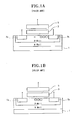
- FIGS. 1 a and 1 b general activating principles of a flash memory device and Fowler-Nordheim Tunneling (FN Tunneling) phenomenon are explained below.
- FIG. 1 a is a schematic sectional view of a general stacked gate cell flash memory transistor showing FN tunneling phenomena in the case of programming
- FIG. 1 b shows the stacked gate cell flash memory in the case of erasing.
- FIGS. 1 a and 1 b as regards the general principles of the flash memory device, programming is carried out through implanting electrons into a floating gate 3 by utilizing the Fowler-Nordheim Tunneling phenomenon, and erasing activity is carried out through discharging the electrons.
- the Fowler-Nordheim Tunneling phenomenon which is a kind of quantum mechanical tunneling of electrons
- a classic mechanical phenomenon can occur in the quantum mechanics such as electrons may not jump over the barrier thereof, however, although the energy level of electrons is lower than the energy barrier, electrons can pass through the barrier when a high electric field above 10MV/cm is produced by the application of high voltage, or the barrier is very thin.
- the high voltage means that it is higher than the gate voltage of 1.8 to 3.3 V, which is employed for the reading activity of a flash memory device.
- FIG. 2 is a schematic view of the conventional stacked gate cell flash memory device in section showing conventional patterning of a control gate.
- a floating gate 25 is first formed by depositing a conductive layer for the floating gate on a semiconductor substrate 21 and patterning it, and then a conductive layer for a control gate is deposited on the semiconductor substrate 21 including the floating gate 25 , next photoresist materials (not shown) are sprayed on the conductive layer.
- a photoresist film pattern 31 is formed by exposing and developing the photoresist materials with photolithography technology and a control gate 29 is formed by patterning of the conductive layer with using the photoresist film pattern as a mask.
- an object of the present invention is to provide a method for fabricating a flash memory device, which is capable of increasing conservation effects of electrons implanted into a floating gate by a Fowler-Nordheim Tunneling phenomenon and improving reliability of the activity characteristics of the flash memory device.
- Another object of the present invention is to provide a method for fabricating a flash memory device, which can easily perform patterning of the memory device, because interactions between neighboring patterns can be reduced by decreasing the size of the mask pattern.
- Still another object of the present invention is to provide a method for fabricating a flash memory device, which can minimize the unsymmetrical property of the lower part of the control gate resulting from misalignment of the mask, because contact areas with a silicon substrate can be increased by forming a tail part in the lower part of the control gate.
- a method for fabricating a flash memory device comprising the steps of: forming a floating gate oxide film on a silicon substrate, forming a floating gate on the floating gate oxide film, forming a control gate oxide film on the floating gate, forming a control gate including slant side surfaces on the control gate oxide film.
- a flash memory device comprising: a floating gate oxide film formed on a silicon substrate, a floating gate formed on the floating gate oxide film, a control gate oxide film formed on the floating gate, and a control gate formed on the control gate oxide film and including slant side surfaces.
- FIG. 1A is a schematic sectional view of a general stacked gate cell flash memory transistor showing FN tunneling phenomenon in the case of programming
- FIG. 1B is a schematic sectional view of a general stacked gate cell flash memory transistor in the case of erasing
- FIG. 2 is a schematic view of the conventional stacked gate cell flash memory device in section showing conventional patterning of the control gate
- FIG. 3 is a sectional view illustrating a method for fabricating a flash memory device in accordance with the present invention
- FIGS. 4A and 4B are sectional views illustrating the flash memory device and fabricating method thereof in accordance with the present invention.
- FIG. 3 is a sectional view illustrating a flash memory device and fabricating method thereof in accordance with the present invention.
- a floating gate oxide film 43 is formed on a silicon substrate 41 , and a floating gate 45 is formed on the oxide film 43 .
- a control gate oxide film 47 is formed on the floating gate 45 , and a control gate 49 is formed on the control gate oxide film 47 .
- side parts 49 a of the control gate 49 are formed slantly, and tails 49 b are formed on a lower part thereof.
- a width L 2 of a photoresist film pattern 51 which is used to form the control gate 49 , is smaller than a conventional width L, and a thickness T 2 of the floating gate 45 is increased to one and a half times of a conventional thickness T 1 shown in FIG. 2.
- FIGS. 4A and 4B are sectional views illustrating a method for fabricating a flash memory device in accordance with the present invention.
- a floating gate oxide film 43 is formed on a silicon substrate 41 , a first polysilicon layer for making floating gate is deposited on the floating gate oxide 43 , first photoresist materials are sprayed on the polysilicon layer, exposing and developing processes and selective patterning of the photoresist materials are carried out by employing photolithography technology to produce a first photoresist film pattern (not shown), and then selective patterning of the first polysilicon layer is carried out using the first photoresist film pattern (not shown) as a mask, resulting in production of a floating gate 45 .
- the first polysilicon layer deposited to form the floating gate 45 is formed thickly to make the side walls of the control gate, which will be made in the following process, thicker than that of the conventional side walls.
- a control gate oxide film 47 is deposited on the entire surfaces of the silicon substrate 41 and the floating gate 45 after removing the first photoresist film pattern (not shown), and a second polysilicon layer 49 is deposited on the control gate oxide film to form the control gate.
- second photoresist materials are sprayed on the second polysilicon layer 49 , and exposing, developing and selective patterning of the photoresist materials are carried out by photolithography technology, resulting in the production of the second photoresist film pattern 51 .
- the second photoresist film pattern 51 has a smaller width L 2 than the conventional width L.
- a control gate 49 a with slant side walls is formed by selective patterning of the second polysilicon layer 49 using the second photoresist film pattern 51 as a mask.
- tail parts 49 b are formed at lower part of the control gate 49 b , resulting in increase of the contact areas of the silicon substrate 41 .
- the present invention it is possible to make the width of the photoresist film pattern smaller than that of the conventional case, thereby securing adequate intervals between the neighboring patterns. Also, it is possible to make the side walls of the control gate thicker than the conventional case while the width of the photoresist film pattern is made smaller than that of the conventional case.
- the characteristics of the flash memory device is improved based on the increase of the thickness of the floating gate and enlargement of the capability of preventing the electrons from tunneling through channels.
Landscapes
- Non-Volatile Memory (AREA)
- Semiconductor Memories (AREA)
Abstract
A flash memory device and fabricating method thereof. The fabricating method comprises the steps of: forming a floating gate oxide film on a silicon substrate, forming a floating gate on the floating gate oxide film, forming a control gate oxide film on the floating gate, forming a control gate including slant side surfaces on the control gate oxide film; and the flash memory device comprises: a floating gate oxide film formed on a silicon substrate, a floating gate formed on the floating gate oxide film, a control gate oxide film formed on the floating gate, and a control gate formed on the control gate oxide film and including slant side surfaces.
Description
- 1. Field of the Invention
- The present invention relates to a method for fabricating a flash memory device, more particularly to a flash memory device and fabricating method thereof which is capable of increasing activating characteristics and reliability of the device by improving patterning of a control gate.
- 2. Description of the Prior Art
- Referring to FIGS. 1 a and 1 b, general activating principles of a flash memory device and Fowler-Nordheim Tunneling (FN Tunneling) phenomenon are explained below.
- FIG. 1 a is a schematic sectional view of a general stacked gate cell flash memory transistor showing FN tunneling phenomena in the case of programming, and FIG. 1b shows the stacked gate cell flash memory in the case of erasing.
- As shown in FIGS. 1 a and 1 b, as regards the general principles of the flash memory device, programming is carried out through implanting electrons into a floating
gate 3 by utilizing the Fowler-Nordheim Tunneling phenomenon, and erasing activity is carried out through discharging the electrons. - Also, according to situations whether electrons are implanted and existed in the floating gate, reading activity of
logics 1 or 0 is carried out. Theunexplained numeral 1 in the drawing refers to a silicon substrate, thenumeral 5 in the drawing refers to a control gate, thenumeral 7 a refers to a source region, and thenumeral 7 b refers to a drain region. - Further, according to the Fowler-Nordheim Tunneling phenomenon, which is a kind of quantum mechanical tunneling of electrons, when a energy barrier level is higher than that of electrons, a classic mechanical phenomenon can occur in the quantum mechanics such as electrons may not jump over the barrier thereof, however, although the energy level of electrons is lower than the energy barrier, electrons can pass through the barrier when a high electric field above 10MV/cm is produced by the application of high voltage, or the barrier is very thin. In this case, the high voltage means that it is higher than the gate voltage of 1.8 to 3.3 V, which is employed for the reading activity of a flash memory device.
- FIG. 2 is a schematic view of the conventional stacked gate cell flash memory device in section showing conventional patterning of a control gate.
- With regard to a conventional method for fabricating a flash memory device as shown in FIG. 2, a floating gate 25 is first formed by depositing a conductive layer for the floating gate on a
semiconductor substrate 21 and patterning it, and then a conductive layer for a control gate is deposited on thesemiconductor substrate 21 including the floating gate 25, next photoresist materials (not shown) are sprayed on the conductive layer. - Then, a
photoresist film pattern 31 is formed by exposing and developing the photoresist materials with photolithography technology and acontrol gate 29 is formed by patterning of the conductive layer with using the photoresist film pattern as a mask. - However, according to the conventional art as explained above, as side walls of the
control gate 29 are thin when they are subjected to conventional etching, effective transfer of the voltages applied can not be achieved. - Further, as shown in FIG. 2, it is difficult to pattern the
control gate 29 by way of increasing the length L1 of the mask as noted by “A” in FIG. 2 in order to thicken the side walls of thecontrol gate 29, because the intervals S between the conventional patterns become narrower as noted by “S1”. - Also, if a precious photo process is not secured, symmetries of the right and left in a lower part of the control gate is not achieved due to misalignment of the mask, resulting in reliability problems.
- Accordingly, the present invention has been made to solve the above-mentioned problems occurring in the prior art, and an object of the present invention is to provide a method for fabricating a flash memory device, which is capable of increasing conservation effects of electrons implanted into a floating gate by a Fowler-Nordheim Tunneling phenomenon and improving reliability of the activity characteristics of the flash memory device.
- Another object of the present invention is to provide a method for fabricating a flash memory device, which can easily perform patterning of the memory device, because interactions between neighboring patterns can be reduced by decreasing the size of the mask pattern.
- Still another object of the present invention is to provide a method for fabricating a flash memory device, which can minimize the unsymmetrical property of the lower part of the control gate resulting from misalignment of the mask, because contact areas with a silicon substrate can be increased by forming a tail part in the lower part of the control gate.
- In order to accomplish these objects, there is provided a method for fabricating a flash memory device comprising the steps of: forming a floating gate oxide film on a silicon substrate, forming a floating gate on the floating gate oxide film, forming a control gate oxide film on the floating gate, forming a control gate including slant side surfaces on the control gate oxide film.
- In accordance with another aspect of the present invention, there is also provided a flash memory device comprising: a floating gate oxide film formed on a silicon substrate, a floating gate formed on the floating gate oxide film, a control gate oxide film formed on the floating gate, and a control gate formed on the control gate oxide film and including slant side surfaces.
- The above and other objects, features and advantages of the present invention will be more apparent from the following detailed description taken in conjunction with the accompanying drawings, in which:
- FIG. 1A is a schematic sectional view of a general stacked gate cell flash memory transistor showing FN tunneling phenomenon in the case of programming, and FIG. 1B is a schematic sectional view of a general stacked gate cell flash memory transistor in the case of erasing;
- FIG. 2 is a schematic view of the conventional stacked gate cell flash memory device in section showing conventional patterning of the control gate;
- FIG. 3 is a sectional view illustrating a method for fabricating a flash memory device in accordance with the present invention;
- FIGS. 4A and 4B are sectional views illustrating the flash memory device and fabricating method thereof in accordance with the present invention.
- Hereinafter, a preferred embodiment of the present invention will be described with reference to the accompanying drawings.
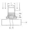
- FIG. 3 is a sectional view illustrating a flash memory device and fabricating method thereof in accordance with the present invention.
- As shown in FIG. 3, in the flash memory device according to the present invention, a floating
gate oxide film 43 is formed on asilicon substrate 41, and afloating gate 45 is formed on theoxide film 43. - Further, a control
gate oxide film 47 is formed on thefloating gate 45, and acontrol gate 49 is formed on the controlgate oxide film 47. In this case,side parts 49 a of thecontrol gate 49 are formed slantly, andtails 49 b are formed on a lower part thereof. Also, a width L2 of aphotoresist film pattern 51, which is used to form thecontrol gate 49, is smaller than a conventional width L, and a thickness T2 of thefloating gate 45 is increased to one and a half times of a conventional thickness T1 shown in FIG. 2. - A patterning process of the control gate in the flash memory device in accordance with the present invention is explained below.
- FIGS. 4A and 4B are sectional views illustrating a method for fabricating a flash memory device in accordance with the present invention.
- According to the method for fabricating a flash memory device in accordance with the present invention, as shown in FIG. 4A, a floating
gate oxide film 43 is formed on asilicon substrate 41, a first polysilicon layer for making floating gate is deposited on the floatinggate oxide 43, first photoresist materials are sprayed on the polysilicon layer, exposing and developing processes and selective patterning of the photoresist materials are carried out by employing photolithography technology to produce a first photoresist film pattern (not shown), and then selective patterning of the first polysilicon layer is carried out using the first photoresist film pattern (not shown) as a mask, resulting in production of afloating gate 45. In this case, the first polysilicon layer deposited to form thefloating gate 45 is formed thickly to make the side walls of the control gate, which will be made in the following process, thicker than that of the conventional side walls. - Then, a control
gate oxide film 47 is deposited on the entire surfaces of thesilicon substrate 41 and thefloating gate 45 after removing the first photoresist film pattern (not shown), and asecond polysilicon layer 49 is deposited on the control gate oxide film to form the control gate. - Next, as shown in FIG. 4B, second photoresist materials are sprayed on the
second polysilicon layer 49, and exposing, developing and selective patterning of the photoresist materials are carried out by photolithography technology, resulting in the production of the secondphotoresist film pattern 51. In this instance, the secondphotoresist film pattern 51 has a smaller width L2 than the conventional width L. - Subsequently, a
control gate 49 a with slant side walls is formed by selective patterning of thesecond polysilicon layer 49 using the secondphotoresist film pattern 51 as a mask. In this case,tail parts 49 b are formed at lower part of thecontrol gate 49 b, resulting in increase of the contact areas of thesilicon substrate 41. - In accordance with the method for fabricating a flash memory device of the present invention, the following advantages are achieved.
- According to the present invention, it is possible to make the width of the photoresist film pattern smaller than that of the conventional case, thereby securing adequate intervals between the neighboring patterns. Also, it is possible to make the side walls of the control gate thicker than the conventional case while the width of the photoresist film pattern is made smaller than that of the conventional case.
- Therefore, it is possible to form the side walls of the control gate slant, to deposit films on them, and to etch the deposited films on the slant side walls so that a part of the deposited films remains as tails in the lower part of the control gate.
- Also, it is possible to minimize the unsymmetrical property of the lower part in the control gate resulting from the misalignment of the mask. That is, as the area of the lower part is increased in comparison with the conventional case, it is possible to secure minimum areas for activating the flash memory device in spite of some misalignment of the mask.
- Further, the characteristics of the flash memory device is improved based on the increase of the thickness of the floating gate and enlargement of the capability of preventing the electrons from tunneling through channels.
- Therefore, it is possible to improve the securing effect of the electrons implanted into the floating gate through the Fowler-Nordheim Tunneling phenomenon by increasing the thickness of the floating gate, resulting in improvement of the reliability and characteristics of the flash memory device.
- Although a preferred embodiment of the present invention has been described for illustrative purposes, those skilled in the art will appreciate that various modifications, additions and substitutions are possible, without departing from the scope and spirit of the invention as disclosed in the accompanying claims.
Claims (6)
1. A flash memory device comprising:
a floating gate oxide film formed on a silicon substrate;
a floating gate formed on the floating gate oxide film;
a control gate oxide film formed on the floating gate; and
a control gate formed on the control gate oxide film and including slant side surfaces.
2. The flash memory device according to claim 1 , wherein the control gate is formed integrally with upper and side surfaces of the floating gate.
3. The flash memory device according to claim 1 , wherein tails are formed on the lower surface of the control gate.
4. A method for fabricating a flash memory device, the method comprising the steps of:
forming a floating gate oxide film on a silicon substrate;
forming a floating gate on the floating gate oxide film;
forming a control gate oxide film on the floating gate;
forming a control gate including slant side surfaces on the control gate oxide film.
5. The method for fabricating a flash memory device according to claim 4 , wherein the control gate is formed integrally with upper and side surfaces of the floating gate.
6. The method for fabricating a flash memory device according to claim 4 , wherein tails are formed on a lower surface of the control gate.
Applications Claiming Priority (2)
| Application Number | Priority Date | Filing Date | Title |
|---|---|---|---|
| KR2002-22119 | 2002-04-23 | ||
| KR10-2002-0022119A KR100464659B1 (en) | 2002-04-23 | 2002-04-23 | Flash memory device and method for fabricating thereof |
Publications (1)
| Publication Number | Publication Date |
|---|---|
| US20030197219A1 true US20030197219A1 (en) | 2003-10-23 |
Family
ID=29208764
Family Applications (1)
| Application Number | Title | Priority Date | Filing Date |
|---|---|---|---|
| US10/330,765 Abandoned US20030197219A1 (en) | 2002-04-23 | 2002-12-27 | Flash memory device and fabricating method therefor |
Country Status (4)
| Country | Link |
|---|---|
| US (1) | US20030197219A1 (en) |
| KR (1) | KR100464659B1 (en) |
| CN (1) | CN1453872A (en) |
| TW (1) | TW200306000A (en) |
Cited By (3)
| Publication number | Priority date | Publication date | Assignee | Title |
|---|---|---|---|---|
| US20060189073A1 (en) * | 2005-02-22 | 2006-08-24 | Intel Corporation | Control gate profile for flash technology |
| US20080061348A1 (en) * | 2006-09-08 | 2008-03-13 | Samsung Electronics Co., Ltd. | Nonvolatile memory structure and method of forming the same |
| US20110084327A1 (en) * | 2009-09-18 | 2011-04-14 | Semiconductor Manufacturing International (Shanghai) Corporation | 3-d electrically programmable and erasable single-transistor non-volatile semiconductor memory device |
Families Citing this family (4)
| Publication number | Priority date | Publication date | Assignee | Title |
|---|---|---|---|---|
| KR100647001B1 (en) * | 2005-03-09 | 2006-11-23 | 주식회사 하이닉스반도체 | Floating gate electrode formation method of flash memory device |
| KR100635199B1 (en) | 2005-05-12 | 2006-10-16 | 주식회사 하이닉스반도체 | Flash memory device and manufacturing method thereof |
| CN105826269B (en) * | 2015-01-07 | 2019-07-02 | 中芯国际集成电路制造(上海)有限公司 | Flash memory and forming method thereof |
| US10211511B2 (en) | 2015-01-23 | 2019-02-19 | Unist (Ulsan National Institute Of Science And Technology) | Terahertz detector using field-effect transistor |
Family Cites Families (3)
| Publication number | Priority date | Publication date | Assignee | Title |
|---|---|---|---|---|
| US5212541A (en) * | 1991-04-18 | 1993-05-18 | National Semiconductor Corporation | Contactless, 5v, high speed eprom/flash eprom array utilizing cells programmed using source side injection |
| KR100311486B1 (en) * | 1995-11-23 | 2002-08-17 | 현대반도체 주식회사 | Semiconductor memory device and manufacturing method thereof |
| JP2924833B2 (en) * | 1996-12-13 | 1999-07-26 | 日本電気株式会社 | Nonvolatile semiconductor memory device and method of manufacturing the same |
-
2002
- 2002-04-23 KR KR10-2002-0022119A patent/KR100464659B1/en not_active Expired - Fee Related
- 2002-12-27 US US10/330,765 patent/US20030197219A1/en not_active Abandoned
- 2002-12-27 TW TW091137742A patent/TW200306000A/en unknown
- 2002-12-31 CN CN02160890A patent/CN1453872A/en active Pending
Cited By (7)
| Publication number | Priority date | Publication date | Assignee | Title |
|---|---|---|---|---|
| US20060189073A1 (en) * | 2005-02-22 | 2006-08-24 | Intel Corporation | Control gate profile for flash technology |
| US7449743B2 (en) * | 2005-02-22 | 2008-11-11 | Intel Corporation | Control gate profile for flash technology |
| DE112006000413B4 (en) * | 2005-02-22 | 2011-05-05 | Intel Corporation, Santa Clara | Non-volatile memory device with chamfered control gate profile and its manufacturing method, associated flash memory and method for storing information in such a memory device |
| US20080061348A1 (en) * | 2006-09-08 | 2008-03-13 | Samsung Electronics Co., Ltd. | Nonvolatile memory structure and method of forming the same |
| US7592664B2 (en) | 2006-09-08 | 2009-09-22 | Samsung Electronics Co., Ltd. | Nonvolatile memory structure and method of forming the same |
| US20110084327A1 (en) * | 2009-09-18 | 2011-04-14 | Semiconductor Manufacturing International (Shanghai) Corporation | 3-d electrically programmable and erasable single-transistor non-volatile semiconductor memory device |
| US8471323B2 (en) * | 2009-09-18 | 2013-06-25 | Semiconductor Manufacturing International (Shanghai) Corporation | 3-D electrically programmable and erasable single-transistor non-volatile semiconductor memory device |
Also Published As
| Publication number | Publication date |
|---|---|
| CN1453872A (en) | 2003-11-05 |
| KR100464659B1 (en) | 2005-01-03 |
| TW200306000A (en) | 2003-11-01 |
| KR20030083443A (en) | 2003-10-30 |
Similar Documents
| Publication | Publication Date | Title |
|---|---|---|
| KR0150048B1 (en) | Flash Y pyrom cell and manufacturing method thereof | |
| KR100607785B1 (en) | Manufacturing method of split gate flash Y pyrom | |
| JPH0855920A (en) | Method for manufacturing semiconductor device | |
| KR20050032443A (en) | Semiconductor device and fabrication method thereof | |
| US20030197219A1 (en) | Flash memory device and fabricating method therefor | |
| KR100199381B1 (en) | Flash Ipyrom Cell Manufacturing Method | |
| US7271059B2 (en) | Semiconductor device and method of fabricating the same | |
| US5856224A (en) | Method of fabricating split-gate flash memory | |
| JPH04212472A (en) | Manufacture of non-volatile semiconductor memory | |
| ITMI971902A1 (en) | PROCESS FOR MANUFACTURING AN ELECTRICALLY PROGRAMMABLE NON-VOLATILE MEMORY DEVICE | |
| US20040043622A1 (en) | Method for preventing hole and electron movement in NROM devices | |
| US6391716B1 (en) | Method for forming poly spacer electron tunnel oxide flash with electric-field enhancing corners for poly to poly erase | |
| JP2004228575A (en) | EEPROM cell and method of manufacturing the same | |
| KR100452313B1 (en) | Nonvolatile Memory Device and Manufacturing Method | |
| KR100665835B1 (en) | Split gate type flash memory device manufacturing method | |
| US6365449B1 (en) | Process for making a non-volatile memory cell with a polysilicon spacer defined select gate | |
| JP2877556B2 (en) | Nonvolatile semiconductor device and method of manufacturing the same | |
| KR100972906B1 (en) | Flash memory cell and manufacturing method thereof | |
| JP2000188344A (en) | Nonvolatile semiconductor memory device and method of manufacturing the same | |
| US20040214433A1 (en) | Flash memory and fabrication method thereof | |
| KR0172274B1 (en) | Non-volatile memory & the manufacturing method thereof | |
| KR100218358B1 (en) | Manufacturing method of flash memory cell | |
| KR100447218B1 (en) | Structure of flash memory device and Method for manufacturing of the same | |
| US20050164453A1 (en) | Method of manufacturing nonvolatile semiconductor storage device | |
| KR100917056B1 (en) | Cell Gate Formation Method of Semiconductor Memory Device |
Legal Events
| Date | Code | Title | Description |
|---|---|---|---|
| AS | Assignment |
Owner name: HYNIX SEMICONDUCTOR INC., KOREA, REPUBLIC OF Free format text: ASSIGNMENT OF ASSIGNORS INTEREST;ASSIGNORS:KIM, JONG IL;HWANG, CHOONG HO;REEL/FRAME:013626/0385 Effective date: 20021025 |
|
| STCB | Information on status: application discontinuation |
Free format text: ABANDONED -- FAILURE TO RESPOND TO AN OFFICE ACTION |