US20030196881A1 - Fastening of a contact element - Google Patents
Fastening of a contact element Download PDFInfo
- Publication number
- US20030196881A1 US20030196881A1 US10/417,826 US41782603A US2003196881A1 US 20030196881 A1 US20030196881 A1 US 20030196881A1 US 41782603 A US41782603 A US 41782603A US 2003196881 A1 US2003196881 A1 US 2003196881A1
- Authority
- US
- United States
- Prior art keywords
- contact
- element according
- holder
- tabs
- contact element
- Prior art date
- Legal status (The legal status is an assumption and is not a legal conclusion. Google has not performed a legal analysis and makes no representation as to the accuracy of the status listed.)
- Granted
Links
- 238000003466 welding Methods 0.000 claims description 8
- 238000013017 mechanical damping Methods 0.000 claims 1
- 238000003780 insertion Methods 0.000 description 2
- 230000037431 insertion Effects 0.000 description 2
- 238000004519 manufacturing process Methods 0.000 description 2
- 238000000034 method Methods 0.000 description 2
- 238000010276 construction Methods 0.000 description 1
- 230000001419 dependent effect Effects 0.000 description 1
- 238000010586 diagram Methods 0.000 description 1
Images


Classifications
-
- H—ELECTRICITY
- H01—ELECTRIC ELEMENTS
- H01H—ELECTRIC SWITCHES; RELAYS; SELECTORS; EMERGENCY PROTECTIVE DEVICES
- H01H11/00—Apparatus or processes specially adapted for the manufacture of electric switches
- H01H11/04—Apparatus or processes specially adapted for the manufacture of electric switches of switch contacts
- H01H11/041—Apparatus or processes specially adapted for the manufacture of electric switches of switch contacts by bonding of a contact marking face to a contact body portion
- H01H11/042—Apparatus or processes specially adapted for the manufacture of electric switches of switch contacts by bonding of a contact marking face to a contact body portion by mechanical deformation
-
- H—ELECTRICITY
- H01—ELECTRIC ELEMENTS
- H01H—ELECTRIC SWITCHES; RELAYS; SELECTORS; EMERGENCY PROTECTIVE DEVICES
- H01H11/00—Apparatus or processes specially adapted for the manufacture of electric switches
- H01H2011/0087—Welding switch parts by use of a laser beam
-
- H—ELECTRICITY
- H01—ELECTRIC ELEMENTS
- H01H—ELECTRIC SWITCHES; RELAYS; SELECTORS; EMERGENCY PROTECTIVE DEVICES
- H01H11/00—Apparatus or processes specially adapted for the manufacture of electric switches
- H01H11/04—Apparatus or processes specially adapted for the manufacture of electric switches of switch contacts
- H01H11/041—Apparatus or processes specially adapted for the manufacture of electric switches of switch contacts by bonding of a contact marking face to a contact body portion
- H01H2011/047—Apparatus or processes specially adapted for the manufacture of electric switches of switch contacts by bonding of a contact marking face to a contact body portion on both sides of the contact body portion
Definitions
- the invention relates to a construction of a contact element for the introduction of an electrical current into an electrical switch element, in which the contact element includes an electrical contact which is fastened in a contact holder of the switch element.
- the special contact material has to be riveted or welded to the contact holder.
- the invention has as its object to provide a contact fastening which does not damage the previously produced contact surfaces. Moreover an optimum electrical connection must result. The contact support must not be deformed hereby.
- the contact element including an electrical contact which is fastened in a contact holder of the switch element, with the contact being inserted into a bore of the contact holder and being connected to the contact holder in regions of opposite overlaps.
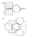
- FIGS. 1 and 2 show one possible alternative embodiment of a spherical contact to be fastened by laser welding
- FIGS. 3 and 4 show a possible alternative embodiment of a spherical contact to be fixed to a contact holder by special holding tabs and by permanently fastening with a special stamping,
- FIGS. 5 and 6 show the alternative embodiment of FIGS. 3 and 4, though without the use of holding tabs.
- FIG. 1 shows, by way of example, a spherical contact 1 , which is held by bent-down holding tabs 2 .
- the welding tabs 3 bent upward on the opposite side, serve in this case to weld the ball 1 to the support strip material 4 .
- the left-hand sectional half shows the state before welding the portion 1 to the weld tab 3 ; and the right-hand half of the diagram shows the welded state 5 which has been produced by a laser beam, shown symbolically as ( 6 ).
- the volume of welding material can be defined by the height of the welding tab 3 in order to obtain an optimum weld 5 .
- the angle of bend “alpha” can be chosen so that the ball 1 snaps into the contact holder on assembly and is held between the tabs 2 and 3 .
- FIG. 2 shows the blank of the contact holder 4 and a bore 11 formed in the blank and serving for insertion of the contact 1 , for which the tabs 2 , 3 have to be bent out of the plane of the contact holder before or during insertion of the contact.
- the bend lines 7 at which the tabs are bent are shown symbolically.
- the tabs 2 and 3 are arranged alternately and serve for optimum holding of the contact 1 with three each of bent up and bent down tabs. Embodiments are also conceivable with two each of the tabs 2 and 3 .
- the number and arrangement of the tabs also depends on the shape of the contact. For example, if a cylindrical contact 1 b (not shown) is used, the arrangement of the tabs would logically correspond.
- FIG. 3 shows, by way of example, a spherical contact 1 which in this case is held on one side downward in the contact holder by holding tabs 2 , and is stamped in the interspaces at three places by two dies 8 a and 8 b , so that the contact overlaps the contact holder 4 in the region of these deformations 9 and is hereby held positively and frictionally.
- FIG. 4 shows the blank of the contact holder with the bore 11 and the bend lines 7 .
- the spherical contact 1 is shown schematically with the stamping regions 9 dashed. In this example, three stamping regions over the periphery are shown.
- FIGS. 5 and 6 show an alternative embodiment similar to FIGS. 3 and 4, so that like components are identified with the same reference numerals. Only the holding tabs 2 are omitted in the constructional form of FIGS. 5 and 6, the contact 1 before stamping is not fixed in the contact holder 4 .
- the blank of the contact holder accordingly has (corresponding to the cross section of the contact 1 ) a circular bore 11 .
- the contact 1 is fixed in the contact holder 4 in the middle of, and symmetrically of the plane of, the contact holder 4 .
- the regions 9 deformed during stamping form the overlapping of the contact 1 with the contact holder 4 by means of which the contact is held positively and frictionally.
- the advantage of the invention is that the contact can be very easily mounted in the contact holder. Both the positioning and the fixing of the contact are ensured.
- the electrical connection can be produced by welding or stamping in the region of an opposite overlapping, thus ensuring that the support material is not deformed and the contact surface is not damaged.
Landscapes
- Engineering & Computer Science (AREA)
- Manufacturing & Machinery (AREA)
- Manufacture Of Switches (AREA)
- Contacts (AREA)
- Coupling Device And Connection With Printed Circuit (AREA)
- Connections Effected By Soldering, Adhesion, Or Permanent Deformation (AREA)
Abstract
Description
- The invention relates to a construction of a contact element for the introduction of an electrical current into an electrical switch element, in which the contact element includes an electrical contact which is fastened in a contact holder of the switch element.
- In order for an electrical switch element to have an optimum contact resistance, the special contact material has to be riveted or welded to the contact holder.
- It is known to weld these contacts to the contact holder by resistance welding methods. Likewise it is state of the art to rivet contacts into a contact holder. These rivets can be pre-produced rivets, or can be present as a wire section for riveting.
- The disadvantage of the method practiced up to now is that, particularly with thin support strips (e.g., 0.05 mm), the material thickness ratios differ greatly between the parts to be welded, which leads to poor welds and a variable manufacturing process. With contacts welded on both sides, this problem becomes even more severe.
- When riveting contacts, a given value of riveting force is necessary to form the rivet such that the rivet holds stably in the bore, and a good electrical contact is present. Furthermore, a high quality contact surface has to be produced by the riveting pressure. Thin support strips are thereby deformed, so that a properly functioning part does not result.
- The disadvantage furthermore exists that high quality coated contact surfaces can become damaged.
- The invention has as its object to provide a contact fastening which does not damage the previously produced contact surfaces. Moreover an optimum electrical connection must result. The contact support must not be deformed hereby.
- Both single-sided and double-sided contacts can be made. A more stable manufacturing process, particularly when integrated into a multi-stage tool, has to be ensured.
- The solution must in particular be suitable for very thin support strips (contact holders). It must be possible to use the usual contact materials.
- The object is attained according to the invention by the contact element including an electrical contact which is fastened in a contact holder of the switch element, with the contact being inserted into a bore of the contact holder and being connected to the contact holder in regions of opposite overlaps.
- Further features and advantages of the invention will become apparent from the dependent claims.
- Embodiments of the invention are shown in the drawing and are described in detail hereinafter.
- FIGS. 1 and 2 show one possible alternative embodiment of a spherical contact to be fastened by laser welding,
- FIGS. 3 and 4 show a possible alternative embodiment of a spherical contact to be fixed to a contact holder by special holding tabs and by permanently fastening with a special stamping,
- FIGS. 5 and 6 show the alternative embodiment of FIGS. 3 and 4, though without the use of holding tabs.
- FIG. 1 shows, by way of example, a
spherical contact 1, which is held by bent-downholding tabs 2. Thewelding tabs 3, bent upward on the opposite side, serve in this case to weld theball 1 to thesupport strip material 4. - The left-hand sectional half shows the state before welding the
portion 1 to theweld tab 3; and the right-hand half of the diagram shows the welded state 5 which has been produced by a laser beam, shown symbolically as (6). - The volume of welding material can be defined by the height of the
welding tab 3 in order to obtain an optimum weld 5. The angle of bend “alpha” can be chosen so that theball 1 snaps into the contact holder on assembly and is held between thetabs - FIG. 2 shows the blank of the
contact holder 4 and abore 11 formed in the blank and serving for insertion of thecontact 1, for which thetabs bend lines 7 at which the tabs are bent are shown symbolically. In this special case of use, thetabs contact 1 with three each of bent up and bent down tabs. Embodiments are also conceivable with two each of thetabs - The number and arrangement of the tabs also depends on the shape of the contact. For example, if a cylindrical contact 1 b (not shown) is used, the arrangement of the tabs would logically correspond.
- FIG. 3 shows, by way of example, a
spherical contact 1 which in this case is held on one side downward in the contact holder by holdingtabs 2, and is stamped in the interspaces at three places by twodies 8 a and 8 b, so that the contact overlaps thecontact holder 4 in the region of thesedeformations 9 and is hereby held positively and frictionally. - The fact is decisive here that only
short regions 9 of thecontact holder 4 are concerned in the stamping. Thecontact holder 4 remains free from deformation, and the underside curve around the hole remains small. Moreover, thecontact surface 10 of thecontact 1 remains unaffected and is thus not damaged. - In order to obtain a good positioning of the
contact 1 in thecontact holder 4 and also a good fastening of the contact, it is recommended to stamp thecontact 1 from both sides symmetrically toward the upper or lower side of the contact holder. - FIG. 4 shows the blank of the contact holder with the
bore 11 and thebend lines 7. Thespherical contact 1 is shown schematically with thestamping regions 9 dashed. In this example, three stamping regions over the periphery are shown. - FIGS. 5 and 6 show an alternative embodiment similar to FIGS. 3 and 4, so that like components are identified with the same reference numerals. Only the
holding tabs 2 are omitted in the constructional form of FIGS. 5 and 6, thecontact 1 before stamping is not fixed in thecontact holder 4. The blank of the contact holder accordingly has (corresponding to the cross section of the contact 1) acircular bore 11. By symmetrical action on the upper and lower side of the contact by the stamping die, and by the use of at least threepairs 8 a, 8 b of stamping dies uniformly distributed over the periphery, it can however be ensured that thecontact 1 is fixed in thecontact holder 4 in the middle of, and symmetrically of the plane of, thecontact holder 4. In this embodiment example also, theregions 9 deformed during stamping form the overlapping of thecontact 1 with thecontact holder 4 by means of which the contact is held positively and frictionally. - The advantage of the invention is that the contact can be very easily mounted in the contact holder. Both the positioning and the fixing of the contact are ensured. The electrical connection can be produced by welding or stamping in the region of an opposite overlapping, thus ensuring that the support material is not deformed and the contact surface is not damaged.
Claims (16)
Applications Claiming Priority (4)
| Application Number | Priority Date | Filing Date | Title |
|---|---|---|---|
| DE10217666.3 | 2002-04-19 | ||
| DE10217666 | 2002-04-19 | ||
| DE10257985A DE10257985A1 (en) | 2002-04-19 | 2002-12-12 | Attachment of a contact element |
| DE10257985.7 | 2002-12-12 |
Publications (2)
| Publication Number | Publication Date |
|---|---|
| US20030196881A1 true US20030196881A1 (en) | 2003-10-23 |
| US6812418B2 US6812418B2 (en) | 2004-11-02 |
Family
ID=28676068
Family Applications (1)
| Application Number | Title | Priority Date | Filing Date |
|---|---|---|---|
| US10/417,826 Expired - Fee Related US6812418B2 (en) | 2002-04-19 | 2003-04-17 | Fastening of a contact element |
Country Status (3)
| Country | Link |
|---|---|
| US (1) | US6812418B2 (en) |
| EP (1) | EP1355331A3 (en) |
| JP (1) | JP2003317561A (en) |
Citations (5)
| Publication number | Priority date | Publication date | Assignee | Title |
|---|---|---|---|---|
| US3555210A (en) * | 1969-05-27 | 1971-01-12 | Oak Electro Netics Corp | Switch contact mounting for rotary switches |
| US4414735A (en) * | 1980-04-16 | 1983-11-15 | Crouzet | Process for making conductor element with double contact face |
| US5057746A (en) * | 1990-10-12 | 1991-10-15 | Texas Instruments Incorporated | Current sensing relay |
| US6041497A (en) * | 1996-06-27 | 2000-03-28 | Murata Manufacturing Co., Ltd. | Method of making a connection terminal |
| US6143998A (en) * | 1996-07-29 | 2000-11-07 | Marquardt Gmbh | Electrical switch, and method of manufacturing such a switch |
Family Cites Families (7)
| Publication number | Priority date | Publication date | Assignee | Title |
|---|---|---|---|---|
| DE200822C (en) * | 1906-05-31 | |||
| US2700087A (en) * | 1949-05-31 | 1955-01-18 | Cutler Hammer Inc | Electrical contact member |
| GB1265309A (en) * | 1968-08-09 | 1972-03-01 | ||
| JPS542909B2 (en) * | 1971-12-09 | 1979-02-15 | ||
| US4025143A (en) * | 1975-06-10 | 1977-05-24 | Rozmus John J | Electrical contacts |
| DE2947811C2 (en) * | 1979-11-28 | 1983-06-16 | Leopold Kostal GmbH & Co KG, 5880 Lüdenscheid | Contact body |
| JP3034011B2 (en) * | 1990-10-31 | 2000-04-17 | アルプス電気株式会社 | Manufacturing method of sliding contact |
-
2003
- 2003-03-20 EP EP03006336A patent/EP1355331A3/en not_active Withdrawn
- 2003-04-17 US US10/417,826 patent/US6812418B2/en not_active Expired - Fee Related
- 2003-04-21 JP JP2003115367A patent/JP2003317561A/en active Pending
Patent Citations (5)
| Publication number | Priority date | Publication date | Assignee | Title |
|---|---|---|---|---|
| US3555210A (en) * | 1969-05-27 | 1971-01-12 | Oak Electro Netics Corp | Switch contact mounting for rotary switches |
| US4414735A (en) * | 1980-04-16 | 1983-11-15 | Crouzet | Process for making conductor element with double contact face |
| US5057746A (en) * | 1990-10-12 | 1991-10-15 | Texas Instruments Incorporated | Current sensing relay |
| US6041497A (en) * | 1996-06-27 | 2000-03-28 | Murata Manufacturing Co., Ltd. | Method of making a connection terminal |
| US6143998A (en) * | 1996-07-29 | 2000-11-07 | Marquardt Gmbh | Electrical switch, and method of manufacturing such a switch |
Also Published As
| Publication number | Publication date |
|---|---|
| EP1355331A2 (en) | 2003-10-22 |
| JP2003317561A (en) | 2003-11-07 |
| US6812418B2 (en) | 2004-11-02 |
| EP1355331A3 (en) | 2004-03-17 |
Similar Documents
| Publication | Publication Date | Title |
|---|---|---|
| KR101389172B1 (en) | Female terminal fitting and production method therefor | |
| US6905343B1 (en) | Interposer assembly | |
| CA2154958A1 (en) | Boardlock assembly | |
| US4546409A (en) | Device for cooling semiconductor elements | |
| US11824298B2 (en) | Multi-part contact | |
| KR20200069973A (en) | Press-fit pin, semiconductor package having the same and method for manufacturing the press-fit pin | |
| US6761597B2 (en) | Terminal structure with spring-loaded contact | |
| CN1046595C (en) | Battery and circuit backplane with terminals | |
| US6812418B2 (en) | Fastening of a contact element | |
| US20010027991A1 (en) | Conductive element and manufacturing method thereof | |
| WO2004098810A1 (en) | Process for joining together components | |
| US6723950B1 (en) | Method for welding thin tabs in wide slots | |
| US4367430A (en) | Shadow mask type color cathode-ray tube | |
| JP2004134241A (en) | Push-button switch member and its manufacturing method | |
| JP2008159357A (en) | Cylindrical secondary battery | |
| JPH0960617A (en) | Joining member and joining method for aluminum plate and sheet metal | |
| JP2007527816A (en) | Radius arm for automobile wheel suspension | |
| US4489228A (en) | Welding method and thermostat produced | |
| US6725537B2 (en) | Method of connecting circuit element | |
| US3971907A (en) | Electrical assembly, electrical contact and method of mounting an electrical contact | |
| JP4922777B2 (en) | How to connect terminals to metal plates | |
| US11855506B2 (en) | Base assembly of voice coil motor and voice coil motor | |
| CN219510588U (en) | Hardware support with elastic structure | |
| JP2002279875A (en) | pressure switch | |
| JP3056358B2 (en) | How to join metal contacts |
Legal Events
| Date | Code | Title | Description |
|---|---|---|---|
| AS | Assignment |
Owner name: KRAMSKI GMBH, GERMANY Free format text: ASSIGNMENT OF ASSIGNORS INTEREST;ASSIGNORS:KRAMSKI, WIESTAW;SCHWEIZER, JOACHIM;FRETZ, EWALD;REEL/FRAME:013983/0637 Effective date: 20030415 |
|
| AS | Assignment |
Owner name: KRAMSKI GMBH, GERMANY Free format text: CORRECTIVE COVERSHEET TO CORRECT THE ASSIGNEE'S ADDRESS PREVIOUSLY RECORDED ON REEL 013983, FRAME 0637.;ASSIGNORS:KRAMSKI, WIESTAW;SCHWEIZER, JOACHIM;FRETZ, EWALD;REEL/FRAME:014619/0462 Effective date: 20030415 |
|
| REMI | Maintenance fee reminder mailed | ||
| LAPS | Lapse for failure to pay maintenance fees | ||
| STCH | Information on status: patent discontinuation |
Free format text: PATENT EXPIRED DUE TO NONPAYMENT OF MAINTENANCE FEES UNDER 37 CFR 1.362 |
|
| FP | Expired due to failure to pay maintenance fee |
Effective date: 20081102 |