US20030192470A1 - Doped semiconductor wafer of float zone pulled semiconductor material, and process for producing the semiconductor wafer - Google Patents
Doped semiconductor wafer of float zone pulled semiconductor material, and process for producing the semiconductor wafer Download PDFInfo
- Publication number
- US20030192470A1 US20030192470A1 US10/410,812 US41081203A US2003192470A1 US 20030192470 A1 US20030192470 A1 US 20030192470A1 US 41081203 A US41081203 A US 41081203A US 2003192470 A1 US2003192470 A1 US 2003192470A1
- Authority
- US
- United States
- Prior art keywords
- single crystal
- magnetic field
- molten material
- semiconductor wafer
- float zone
- Prior art date
- Legal status (The legal status is an assumption and is not a legal conclusion. Google has not performed a legal analysis and makes no representation as to the accuracy of the status listed.)
- Granted
Links
Images


Classifications
-
- C—CHEMISTRY; METALLURGY
- C30—CRYSTAL GROWTH
- C30B—SINGLE-CRYSTAL GROWTH; UNIDIRECTIONAL SOLIDIFICATION OF EUTECTIC MATERIAL OR UNIDIRECTIONAL DEMIXING OF EUTECTOID MATERIAL; REFINING BY ZONE-MELTING OF MATERIAL; PRODUCTION OF A HOMOGENEOUS POLYCRYSTALLINE MATERIAL WITH DEFINED STRUCTURE; SINGLE CRYSTALS OR HOMOGENEOUS POLYCRYSTALLINE MATERIAL WITH DEFINED STRUCTURE; AFTER-TREATMENT OF SINGLE CRYSTALS OR A HOMOGENEOUS POLYCRYSTALLINE MATERIAL WITH DEFINED STRUCTURE; APPARATUS THEREFOR
- C30B29/00—Single crystals or homogeneous polycrystalline material with defined structure characterised by the material or by their shape
- C30B29/02—Elements
- C30B29/06—Silicon
-
- C—CHEMISTRY; METALLURGY
- C30—CRYSTAL GROWTH
- C30B—SINGLE-CRYSTAL GROWTH; UNIDIRECTIONAL SOLIDIFICATION OF EUTECTIC MATERIAL OR UNIDIRECTIONAL DEMIXING OF EUTECTOID MATERIAL; REFINING BY ZONE-MELTING OF MATERIAL; PRODUCTION OF A HOMOGENEOUS POLYCRYSTALLINE MATERIAL WITH DEFINED STRUCTURE; SINGLE CRYSTALS OR HOMOGENEOUS POLYCRYSTALLINE MATERIAL WITH DEFINED STRUCTURE; AFTER-TREATMENT OF SINGLE CRYSTALS OR A HOMOGENEOUS POLYCRYSTALLINE MATERIAL WITH DEFINED STRUCTURE; APPARATUS THEREFOR
- C30B13/00—Single-crystal growth by zone-melting; Refining by zone-melting
- C30B13/08—Single-crystal growth by zone-melting; Refining by zone-melting adding crystallising materials or reactants forming it in situ to the molten zone
- C30B13/10—Single-crystal growth by zone-melting; Refining by zone-melting adding crystallising materials or reactants forming it in situ to the molten zone with addition of doping materials
-
- C—CHEMISTRY; METALLURGY
- C30—CRYSTAL GROWTH
- C30B—SINGLE-CRYSTAL GROWTH; UNIDIRECTIONAL SOLIDIFICATION OF EUTECTIC MATERIAL OR UNIDIRECTIONAL DEMIXING OF EUTECTOID MATERIAL; REFINING BY ZONE-MELTING OF MATERIAL; PRODUCTION OF A HOMOGENEOUS POLYCRYSTALLINE MATERIAL WITH DEFINED STRUCTURE; SINGLE CRYSTALS OR HOMOGENEOUS POLYCRYSTALLINE MATERIAL WITH DEFINED STRUCTURE; AFTER-TREATMENT OF SINGLE CRYSTALS OR A HOMOGENEOUS POLYCRYSTALLINE MATERIAL WITH DEFINED STRUCTURE; APPARATUS THEREFOR
- C30B13/00—Single-crystal growth by zone-melting; Refining by zone-melting
- C30B13/26—Stirring of the molten zone
Definitions
- the invention relates to a doped semiconductor wafer of float zone-pulled semiconductor material and to a process for producing the semiconductor wafer.
- the process comprises the production of a doped single crystal by float zone pulling (floating zone crystal growth, FZ method) and the division of the single crystal into semiconductor wafers.
- float zone pulling floating zone crystal growth, FZ method
- FZ method floating zone crystal growth, FZ method
- a molten material which has been produced using an induction coil is exposed to at least one rotating magnetic field and is solidified.
- the single crystal which is formed during the solidification of the molten material is rotated.
- Striations are macroscopic dopant fluctuations. They are usually quantified by carrying out a spreading resistance analysis on the semiconductor wafer.
- the radial macroscopic resistance distribution is measured by the four-point methods described in ASTM F 84, taking a mean over a length of several millimeters.
- neutron doping has a large number of drawbacks.
- the method is only suitable for semiconductor material with a resistance of approximately 3 to approximately 800 Ohm*cm. Radiation damage which has to be annealed by a thermal aftertreatment is inevitably produced. Nevertheless, it is impossible to prevent a reduction in the minority charge carrier life. Furthermore, necessary decay times, the thermal aftertreatment and associated conveying operations make the method time-consuming and expensive.
- the present invention is directed to a doped semiconductor wafer of float zone-pulled semiconductor material which contains a dopant added to a molten material and has a radial macroscopic resistance distribution of less than 12% and striations of ⁇ 10% to +10%.
- the present invention is also directed to a process for producing a doped semiconductor wafer by float zone pulling of a single crystal and dividing up the single crystal, in which process, during the float zone pulling, a molten material which is produced using an induction coil is doped with a dopant, exposed to at least one rotating magnetic field and is solidified, and the single crystal which is formed during the solidification of the molten material is rotated, the single crystal and the magnetic field being rotated with opposite directions of rotation and the magnetic field having a frequency of 400 to 700 Hz.
- the selected frequency range is important because in this range the power required to drive the magnet system is low and, at the same time, the flow of molten material can be influenced most successfully within the context of the invention.
- a silicon semiconductor wafer produced using the process of the invention has a radial macroscopic resistance distribution which is similar to that of a neutron-doped semiconductor wafer.
- the wafer can have a minority charge carrier life of at least 100: ⁇ sec.
- the resistance ranges there is no restriction similar to that encountered with neutron-doped material.
- the resistances may be from below 3 Ohm*cm to above 800 Ohm*cm, preferably from 0.05 to 8000 Ohm*cm.
- the process of the invention has the advantage that fluctuations in the resistances of the semiconductor wafers which originate from one single crystal are less than +/ ⁇ 8%.
- FIG. 1 shows an arrangement which is suitable for carrying out the process
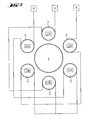
- FIG. 2 shows a preferred arrangement of a magnet system around a single crystal
- FIGS. 3 and 4 reproduce the flow conditions in the molten material which have been calculated in simulation calculations, the figures in each case illustrating only one of two symmetrical halves of a section through the molten material;
- FIG. 5 shows the resistance scatter and profile position for silicon wafers which originate from an FZ single crystal which has been pulled with a rotating magnetic field in accordance with the invention
- FIG. 6 shows a comparative illustration of measurements of the spreading resistance values for silicon semiconductor wafers with a diameter of 4 inches.
- the top diagram FIG. 6 a shows the values for material which has been pulled with a rotating magnetic field in accordance with the invention, while the lower diagram FIG. 6 b shows the values for material in which the rotating magnetic field was not used.
- FIG. 1 the arrangement illustrated in FIG. 1 comprises a single crystal 4 , which is connected to a polycrystalline stock ingot 1 via a molten material 3 .
- the molten material is produced by an induction coil 2 .
- the induction coil causes material of the stock ingot to melt, and in this way the volume of the molten material is increased.
- a magnet system 5 with at least three poles or a multiple thereof is to be provided, such as for example the system used in a three-phase electric motor with three-pole stator.
- This generates a magnetic field which rotates in the opposite direction to the direction of rotation of the single crystal.
- the magnet system is preferably shielded from thermal radiation and water-cooled. It is also preferable for it to be possible for the field strength of the magnetic field to be varied between 0 and 100% by means of a potentiometer.
- the field lines 6 of the magnetic field are illustrated by arrows in FIG. 1.
- the arrangement illustrated in FIG. 2 comprises a 6 -pole magnet system 5 with three-phase driving. This is formed by six individual magnets (L 1 a -L 3 b ) distributed uniformly around the single crystal, with in each case two opposite poles corresponding, is particularly preferred.
- the dopant distribution in the single crystal is influenced by the flow conditions in the molten material and by boundary layer diffusion.
- the flow in the molten material which is produced by the thermal, Marangoni and electromagnetic forces, has a typical twin-eddy structure, which is illustrated in FIG. 3, in particular for single crystals with large diameters.
- the dopant concentration is lower than in an outer eddy 20 . As long as these differences in concentration are present in the two eddies, making the diffusion boundary layer thickness more uniform has no effect with regard to radial dopant homogenization.
- the flow is directed downward toward the single crystal, which immediately has two drawbacks. Firstly, the downwardly directed flow causes fractions of molten material which contain relatively little dopant to pass to the growth front of the single crystal, while there are higher levels of dopant in the vicinity of the edges. Secondly, particles which originate from the stock ingot also pass to the growth front together with the flow, where they have an adverse effect on the dislocation-free growth of the single crystal.
- FIG. 4 A single-eddy structure 30 of this type is illustrated in FIG. 4.
- the molten material now forms a single area in which the flow in the center is directed upward, i.e. toward the stock ingot.
- dopant is conveyed from the edge regions into the center, so that the dopant concentration in the molten material becomes more uniform.
- the altered flow also forces particles to take a longer route to the growth front. In general, therefore, the particles are left with sufficient time to melt completely before they reach the growth front, so that the dislocation rate is greatly reduced.
- the rotation of the single crystal and the direction of rotation of the magnetic field have to be set in such a way that on average over the course of time an opposite direction of rotation results.
- the rotational speed of the single crystal is at least 1 rpm. If the single crystal is subject to alternating rotation (a periodic change in the direction of rotation), which is also possible in accordance with the invention, the rotation of the crystal taken as an average over the course of time is the decisive factor in defining the direction of rotation of the crystal. It is also possible for the direction of rotation of the magnetic field to be alternated accordingly.
- the single crystal executes a monodirectional rotation in just one direction or an alternating rotation which is taken as an average over the course of time. This results in a rotation in this direction, while the magnetic field rotates in the opposite direction.
- the single crystal executes a monodirectional rotation, while the direction of rotation of the magnetic field alternates but taken as an average over the course of time is directed in the opposite direction.
- the field strength of the magnetic field has to be matched to the prevailing process conditions.
- the form and scatter of the radial resistance profile can be corrected within wide limits by varying the magnetic field strength.
- the optimum field strength is dependent on other process parameters, such as the frequency of the magnetic field, the diameter and the rotational speed of the single crystal, the pulling rate and the shape of the induction coil used. It is therefore to be determined by tests.
- Tests carried out by the inventors have indicated that the process is preferably used to pull silicon single crystals which have a diameter of at least 3′′ (76.2 mm). Tests also indicate that the field strength of the rotating magnetic field can be in the range from 1 to 20 mT, and particularly preferably from 1 to 2.5 mT.
- the frequency of the rotating magnetic field can be in the range from 400 to 700 Hz, and particularly preferably in the range from 450 to 650 Hz. Above 700 Hz, the action of forces becomes saturated, since the depth of penetration into the molten material is considerably less than the height of the vessel holding the molten material. Furthermore, the technical problems increase, on account of the inevitably higher voltages. Below 400 Hz, the action of the forces becomes too low to achieve the desired effect with reasonable technical outlay.
- the rotating magnetic field may be symmetrical or asymmetrical with respect to the axis of rotation of the single crystal.
- An asymmetrical field can be produced by different driving of individual magnets with a regular arrangement of the individual magnets. It can also be produced by an asymmetrical arrangement of individual magnets or by tilting the regularly arranged individual magnets out of the horizontal plane.
- the first frequency, which drives the outer area of the molten material is from 400 to 700 Hz, particularly preferably 500 Hz, and if the second frequency, which drives the inner area of the molten material, is below 100 Hz, preferably is 50 Hz.
- FIG. 5 shows the resistance scatter and profile position for silicon wafers which originate from an FZ single crystal pulled using a rotating magnetic field in accordance with the invention.
- FIG. 6 shows a comparative illustration of measurements of the spreading resistance values.
- FIG. 6 a shows the values for material which has been pulled using a rotating magnetic field in accordance with the invention, while FIG. 6 b shows the values for material in which the rotating magnetic field was not used.
Landscapes
- Chemical & Material Sciences (AREA)
- Engineering & Computer Science (AREA)
- Crystallography & Structural Chemistry (AREA)
- Materials Engineering (AREA)
- Metallurgy (AREA)
- Organic Chemistry (AREA)
- Crystals, And After-Treatments Of Crystals (AREA)
Abstract
Description
- 1. Field of The Invention
- The invention relates to a doped semiconductor wafer of float zone-pulled semiconductor material and to a process for producing the semiconductor wafer. The process comprises the production of a doped single crystal by float zone pulling (floating zone crystal growth, FZ method) and the division of the single crystal into semiconductor wafers. During the pulling of the single crystal, a molten material which has been produced using an induction coil is exposed to at least one rotating magnetic field and is solidified. The single crystal which is formed during the solidification of the molten material is rotated.
- 2. The Prior Art
- The use of a rotating magnetic field in float zone pulling is described, for example, in DD-263 310 A1. However, the process which is proposed in this document attempts to make the diffusion boundary layer thickness more uniform. However the present invention achieves the most homogeneous distribution of dopants added to the molten material possible and of reducing striations. A homogeneous dopant distribution manifests itself in a tight radial macroscopic resistance distribution.
- Striations are macroscopic dopant fluctuations. They are usually quantified by carrying out a spreading resistance analysis on the semiconductor wafer.
- The radial macroscopic resistance distribution is measured by the four-point methods described in ASTM F 84, taking a mean over a length of several millimeters.
- Hitherto, it has been attempted to homogenize the dopant distribution and therefore reduce the radial resistance variation by varying the crystal rotation, by displacing the induction coil relative to the crystal axis and by changing the shape of the induction coil. A drawback of these measures is that they often lead to an increase in the dislocation rate and to a reduction in the process stability.
- It is also known that very flat radial dopant profiles can be set by neutron doping. However, neutron doping has a large number of drawbacks. For example, the method is only suitable for semiconductor material with a resistance of approximately 3 to approximately 800 Ohm*cm. Radiation damage which has to be annealed by a thermal aftertreatment is inevitably produced. Nevertheless, it is impossible to prevent a reduction in the minority charge carrier life. Furthermore, necessary decay times, the thermal aftertreatment and associated conveying operations make the method time-consuming and expensive.
- The present invention is directed to a doped semiconductor wafer of float zone-pulled semiconductor material which contains a dopant added to a molten material and has a radial macroscopic resistance distribution of less than 12% and striations of −10% to +10%.
- The present invention is also directed to a process for producing a doped semiconductor wafer by float zone pulling of a single crystal and dividing up the single crystal, in which process, during the float zone pulling, a molten material which is produced using an induction coil is doped with a dopant, exposed to at least one rotating magnetic field and is solidified, and the single crystal which is formed during the solidification of the molten material is rotated, the single crystal and the magnetic field being rotated with opposite directions of rotation and the magnetic field having a frequency of 400 to 700 Hz.
- The selected frequency range is important because in this range the power required to drive the magnet system is low and, at the same time, the flow of molten material can be influenced most successfully within the context of the invention.
- A silicon semiconductor wafer produced using the process of the invention, has a radial macroscopic resistance distribution which is similar to that of a neutron-doped semiconductor wafer. The wafer can have a minority charge carrier life of at least 100: μsec. However, with regard to the resistance ranges there is no restriction similar to that encountered with neutron-doped material. For example, the resistances may be from below 3 Ohm*cm to above 800 Ohm*cm, preferably from 0.05 to 8000 Ohm*cm. Furthermore, the process of the invention, has the advantage that fluctuations in the resistances of the semiconductor wafers which originate from one single crystal are less than +/− 8%.
- Other objects and features of the present invention will become apparent from the following detailed description considered in connection with the accompanying drawings which disclose several embodiments of the present invention. It should be understood, however, that the drawings are designed for the purpose of illustration only and not as a definition of the limits of the invention.
- In the drawing, wherein similar reference characters denote similar elements throughout the several views:
- FIG. 1 shows an arrangement which is suitable for carrying out the process;
- FIG. 2 shows a preferred arrangement of a magnet system around a single crystal;
- FIGS. 3 and 4 reproduce the flow conditions in the molten material which have been calculated in simulation calculations, the figures in each case illustrating only one of two symmetrical halves of a section through the molten material;
- FIG. 5 shows the resistance scatter and profile position for silicon wafers which originate from an FZ single crystal which has been pulled with a rotating magnetic field in accordance with the invention; and
- FIG. 6 shows a comparative illustration of measurements of the spreading resistance values for silicon semiconductor wafers with a diameter of 4 inches. The top diagram FIG. 6 a shows the values for material which has been pulled with a rotating magnetic field in accordance with the invention, while the lower diagram FIG. 6b shows the values for material in which the rotating magnetic field was not used.
- Turning now in detail to the drawings, the arrangement illustrated in FIG. 1 comprises a
single crystal 4, which is connected to a polycrystalline stock ingot 1 via amolten material 3. The molten material is produced by aninduction coil 2. During the lowering of the single crystal, some of the molten material solidifies, so that the volume of the single crystal increases. At the same time, the induction coil causes material of the stock ingot to melt, and in this way the volume of the molten material is increased. - According to the invention, a
magnet system 5 with at least three poles or a multiple thereof is to be provided, such as for example the system used in a three-phase electric motor with three-pole stator. This generates a magnetic field which rotates in the opposite direction to the direction of rotation of the single crystal. The magnet system is preferably shielded from thermal radiation and water-cooled. It is also preferable for it to be possible for the field strength of the magnetic field to be varied between 0 and 100% by means of a potentiometer. Thefield lines 6 of the magnetic field are illustrated by arrows in FIG. 1. - The arrangement illustrated in FIG. 2, comprises a 6-
pole magnet system 5 with three-phase driving. This is formed by six individual magnets (L1 a-L3 b) distributed uniformly around the single crystal, with in each case two opposite poles corresponding, is particularly preferred. - The dopant distribution in the single crystal is influenced by the flow conditions in the molten material and by boundary layer diffusion. The flow in the molten material, which is produced by the thermal, Marangoni and electromagnetic forces, has a typical twin-eddy structure, which is illustrated in FIG. 3, in particular for single crystals with large diameters. In the
central eddy 10, which is in contact with a polycrystalline stock ingot, the dopant concentration is lower than in anouter eddy 20. As long as these differences in concentration are present in the two eddies, making the diffusion boundary layer thickness more uniform has no effect with regard to radial dopant homogenization. - In the center, the flow is directed downward toward the single crystal, which immediately has two drawbacks. Firstly, the downwardly directed flow causes fractions of molten material which contain relatively little dopant to pass to the growth front of the single crystal, while there are higher levels of dopant in the vicinity of the edges. Secondly, particles which originate from the stock ingot also pass to the growth front together with the flow, where they have an adverse effect on the dislocation-free growth of the single crystal.
- The inventive application of a rotating magnetic field converts the twin-eddy structure into a single-eddy structure with altered flow conditions. A single-
eddy structure 30 of this type is illustrated in FIG. 4. The molten material now forms a single area in which the flow in the center is directed upward, i.e. toward the stock ingot. As a result, dopant is conveyed from the edge regions into the center, so that the dopant concentration in the molten material becomes more uniform. The altered flow also forces particles to take a longer route to the growth front. In general, therefore, the particles are left with sufficient time to melt completely before they reach the growth front, so that the dislocation rate is greatly reduced. - To optimally exploit the effect, the rotation of the single crystal and the direction of rotation of the magnetic field have to be set in such a way that on average over the course of time an opposite direction of rotation results. The rotational speed of the single crystal is at least 1 rpm. If the single crystal is subject to alternating rotation (a periodic change in the direction of rotation), which is also possible in accordance with the invention, the rotation of the crystal taken as an average over the course of time is the decisive factor in defining the direction of rotation of the crystal. It is also possible for the direction of rotation of the magnetic field to be alternated accordingly.
- The following variants are preferred: the single crystal executes a monodirectional rotation in just one direction or an alternating rotation which is taken as an average over the course of time. This results in a rotation in this direction, while the magnetic field rotates in the opposite direction. Or the single crystal executes a monodirectional rotation, while the direction of rotation of the magnetic field alternates but taken as an average over the course of time is directed in the opposite direction.
- To achieve the change from the twin-eddy structure of FIG. 3 to the single-eddy structure of FIG. 4, the field strength of the magnetic field has to be matched to the prevailing process conditions. The form and scatter of the radial resistance profile can be corrected within wide limits by varying the magnetic field strength.
- The optimum field strength is dependent on other process parameters, such as the frequency of the magnetic field, the diameter and the rotational speed of the single crystal, the pulling rate and the shape of the induction coil used. It is therefore to be determined by tests.
- Tests carried out by the inventors have indicated that the process is preferably used to pull silicon single crystals which have a diameter of at least 3″ (76.2 mm). Tests also indicate that the field strength of the rotating magnetic field can be in the range from 1 to 20 mT, and particularly preferably from 1 to 2.5 mT. The frequency of the rotating magnetic field can be in the range from 400 to 700 Hz, and particularly preferably in the range from 450 to 650 Hz. Above 700 Hz, the action of forces becomes saturated, since the depth of penetration into the molten material is considerably less than the height of the vessel holding the molten material. Furthermore, the technical problems increase, on account of the inevitably higher voltages. Below 400 Hz, the action of the forces becomes too low to achieve the desired effect with reasonable technical outlay.
- The rotating magnetic field may be symmetrical or asymmetrical with respect to the axis of rotation of the single crystal. An asymmetrical field can be produced by different driving of individual magnets with a regular arrangement of the individual magnets. It can also be produced by an asymmetrical arrangement of individual magnets or by tilting the regularly arranged individual magnets out of the horizontal plane.
- Simultaneous application of two rotating magnetic fields with different frequencies and field strengths makes it possible to improve the intimate mixing of the molten material and the radial homogenization of dopants even further. Fields with different frequencies have different penetration depths in the molten material and accordingly act on different areas of molten materials. The direction of rotation of the magnetic fields may be identical or opposite.
- It is preferable if the first frequency, which drives the outer area of the molten material, as stated above is from 400 to 700 Hz, particularly preferably 500 Hz, and if the second frequency, which drives the inner area of the molten material, is below 100 Hz, preferably is 50 Hz.
- Silicon single crystals with a diameter of 4 inches were pulled using the FZ method. Some of the single crystals were pulled using a rotating magnetic field in accordance with the invention, while in others the magnetic field was not used. Then, silicon wafers which had been cut from the single crystals were examined for the distribution of dopants. FIG. 5 shows the resistance scatter and profile position for silicon wafers which originate from an FZ single crystal pulled using a rotating magnetic field in accordance with the invention.
- FIG. 6 shows a comparative illustration of measurements of the spreading resistance values. FIG. 6a shows the values for material which has been pulled using a rotating magnetic field in accordance with the invention, while FIG. 6b shows the values for material in which the rotating magnetic field was not used.
- Accordingly, while a few embodiments of the present invention have been shown and described, it is to be understood that many changes and modifications may be made thereunto without departing from the spirit and scope of the invention as defined in the appended claims.
Claims (8)
Applications Claiming Priority (2)
| Application Number | Priority Date | Filing Date | Title |
|---|---|---|---|
| DE10216609.9 | 2002-04-15 | ||
| DE10216609A DE10216609B4 (en) | 2002-04-15 | 2002-04-15 | Process for producing the semiconductor wafer |
Publications (2)
| Publication Number | Publication Date |
|---|---|
| US20030192470A1 true US20030192470A1 (en) | 2003-10-16 |
| US7025827B2 US7025827B2 (en) | 2006-04-11 |
Family
ID=28685072
Family Applications (1)
| Application Number | Title | Priority Date | Filing Date |
|---|---|---|---|
| US10/410,812 Expired - Fee Related US7025827B2 (en) | 2002-04-15 | 2003-04-10 | Doped semiconductor wafer of float zone pulled semiconductor material, and process for producing the semiconductor wafer |
Country Status (4)
| Country | Link |
|---|---|
| US (1) | US7025827B2 (en) |
| JP (1) | JP2003313087A (en) |
| DE (1) | DE10216609B4 (en) |
| DK (1) | DK176922B1 (en) |
Cited By (5)
| Publication number | Priority date | Publication date | Assignee | Title |
|---|---|---|---|---|
| WO2008125104A1 (en) * | 2007-04-13 | 2008-10-23 | Topsil Simiconductor Materials A/S | Method and apparatus for producing a single crystal |
| CN103866375A (en) * | 2012-12-10 | 2014-06-18 | 有研半导体材料股份有限公司 | Preparation method for doped float zone silicon crystal |
| TWI561690B (en) * | 2014-12-18 | 2016-12-11 | Siltronic Ag | Method for growing a single crystal by crystallizing the single crystal from a float zone |
| US9627280B2 (en) * | 2012-11-29 | 2017-04-18 | Taiwan Semiconductor Manufacturing Company, Ltd. | Methods for probing semiconductor fins through four-point probe and determining carrier concentrations |
| EP3483310A1 (en) * | 2017-11-13 | 2019-05-15 | Sumco Corporation | Monocrystalline silicon production apparatus and monocrystalline silicon production method |
Families Citing this family (8)
| Publication number | Priority date | Publication date | Assignee | Title |
|---|---|---|---|---|
| DE102005063346B4 (en) | 2005-04-06 | 2010-10-28 | Pv Silicon Forschungs Und Produktions Gmbh | Process for producing a monocrystalline Si wafer with approximately round polygonal cross section |
| JP2007145629A (en) * | 2005-11-25 | 2007-06-14 | Canon Machinery Inc | Method and apparatus for growing single crystal |
| KR101020429B1 (en) | 2009-02-12 | 2011-03-08 | 주식회사 엘지실트론 | Single crystal manufacturing method having uniform resistivity and single crystal produced by this method |
| AU2011323843B2 (en) * | 2010-10-25 | 2015-08-20 | Lockheed Martin Corporation | Sonar data collection system |
| JP2013103874A (en) * | 2011-11-11 | 2013-05-30 | Yutaka Kamaike | Silicon and method for manufacturing the same |
| DE102012213506A1 (en) * | 2012-07-31 | 2014-02-06 | Siltronic Ag | Process for producing a single crystal of silicon |
| EP3208366A1 (en) | 2016-02-16 | 2017-08-23 | Siltronic AG | Fz silicon and method to prepare fz silicon |
| JP7528799B2 (en) * | 2021-01-26 | 2024-08-06 | 信越半導体株式会社 | Single crystal pulling apparatus and method |
Citations (4)
| Publication number | Priority date | Publication date | Assignee | Title |
|---|---|---|---|---|
| US5258092A (en) * | 1991-03-22 | 1993-11-02 | Shin-Etsu Handotai Co., Ltd. | Method of growing silicon monocrystalline rod |
| US5349921A (en) * | 1988-03-08 | 1994-09-27 | Her Majesty The Queen In Right Of Canada, As Represented By The Secretary Of State For Defence In Her Britannic Majesty's Government Of The United Kingdom Of Great Britain And Northern Ireland | Growing semiconductor crystalline materials |
| US5556461A (en) * | 1993-06-18 | 1996-09-17 | Shin-Etsu Handotai Co., Ltd. | Method for producing a silicon single crystal by a float-zone method |
| US20020022348A1 (en) * | 1998-07-08 | 2002-02-21 | Kiyofumi Sakaguchi | Semiconductor substrate and production method thereof |
Family Cites Families (2)
| Publication number | Priority date | Publication date | Assignee | Title |
|---|---|---|---|---|
| DE263310C (en) | ||||
| DE10051885B4 (en) * | 2000-10-19 | 2007-07-12 | Siltronic Ag | Method of pulling a single crystal by zone pulling |
-
2002
- 2002-04-15 DE DE10216609A patent/DE10216609B4/en not_active Expired - Fee Related
-
2003
- 2003-04-10 US US10/410,812 patent/US7025827B2/en not_active Expired - Fee Related
- 2003-04-14 JP JP2003109448A patent/JP2003313087A/en active Pending
- 2003-04-15 DK DKPA200300588A patent/DK176922B1/en not_active IP Right Cessation
Patent Citations (4)
| Publication number | Priority date | Publication date | Assignee | Title |
|---|---|---|---|---|
| US5349921A (en) * | 1988-03-08 | 1994-09-27 | Her Majesty The Queen In Right Of Canada, As Represented By The Secretary Of State For Defence In Her Britannic Majesty's Government Of The United Kingdom Of Great Britain And Northern Ireland | Growing semiconductor crystalline materials |
| US5258092A (en) * | 1991-03-22 | 1993-11-02 | Shin-Etsu Handotai Co., Ltd. | Method of growing silicon monocrystalline rod |
| US5556461A (en) * | 1993-06-18 | 1996-09-17 | Shin-Etsu Handotai Co., Ltd. | Method for producing a silicon single crystal by a float-zone method |
| US20020022348A1 (en) * | 1998-07-08 | 2002-02-21 | Kiyofumi Sakaguchi | Semiconductor substrate and production method thereof |
Cited By (9)
| Publication number | Priority date | Publication date | Assignee | Title |
|---|---|---|---|---|
| WO2008125104A1 (en) * | 2007-04-13 | 2008-10-23 | Topsil Simiconductor Materials A/S | Method and apparatus for producing a single crystal |
| US20100107968A1 (en) * | 2007-04-13 | 2010-05-06 | Topsil Simiconductor Materials A/S | Method and apparatus for producing a single crystal |
| EA017453B1 (en) * | 2007-04-13 | 2012-12-28 | Топсил Семикондактор Материалз А/С | Method and apparatus for producing a single crystal |
| US9627280B2 (en) * | 2012-11-29 | 2017-04-18 | Taiwan Semiconductor Manufacturing Company, Ltd. | Methods for probing semiconductor fins through four-point probe and determining carrier concentrations |
| CN103866375A (en) * | 2012-12-10 | 2014-06-18 | 有研半导体材料股份有限公司 | Preparation method for doped float zone silicon crystal |
| TWI561690B (en) * | 2014-12-18 | 2016-12-11 | Siltronic Ag | Method for growing a single crystal by crystallizing the single crystal from a float zone |
| US9932691B2 (en) | 2014-12-18 | 2018-04-03 | Siltronic Ag | Method for growing a single crystal by crystallizing the single crystal from a float zone |
| EP3483310A1 (en) * | 2017-11-13 | 2019-05-15 | Sumco Corporation | Monocrystalline silicon production apparatus and monocrystalline silicon production method |
| CN109778313A (en) * | 2017-11-13 | 2019-05-21 | 胜高股份有限公司 | The manufacturing device and manufacturing method of silicon single crystal |
Also Published As
| Publication number | Publication date |
|---|---|
| DE10216609A1 (en) | 2003-10-30 |
| DE10216609B4 (en) | 2005-04-07 |
| US7025827B2 (en) | 2006-04-11 |
| DK200300588A (en) | 2003-10-16 |
| DK176922B1 (en) | 2010-05-17 |
| JP2003313087A (en) | 2003-11-06 |
Similar Documents
| Publication | Publication Date | Title |
|---|---|---|
| US7025827B2 (en) | Doped semiconductor wafer of float zone pulled semiconductor material, and process for producing the semiconductor wafer | |
| EP2142686B1 (en) | Method for producing a single crystal | |
| Kudla et al. | Crystallization of 640 kg mc-silicon ingots under traveling magnetic field by using a heater-magnet module | |
| US8961685B2 (en) | Method of manufacturing silicon single crystal, silicon single crystal, and wafer | |
| CN1540042A (en) | Method and device for prodn. of silicon single crystal, silicon single crystal, and silicon semiconductor wafers with determined defect distributions | |
| US8932550B2 (en) | Methods for pulling a multicrystalline silicon ingot from a silicon melt | |
| KR101680213B1 (en) | Method for growing silicon single crystal ingot | |
| US20240287704A1 (en) | Method for Producing Nitrogen-Doped Single Crystal Silicon Ingot and Nitrogen-Doped Single Crystal Silicon Ingot | |
| Robertson Jr et al. | Magnetic field effects on float-zone Si crystal growth: III. Strong axial fields | |
| EP0504929B1 (en) | Method of growing silicon monocrystalline rod | |
| US20020124791A1 (en) | Silicon wafer and method for producing the same | |
| TW201531666A (en) | Measurement apparatus | |
| JP2567539B2 (en) | FZ method silicon single crystal ingot growth method and apparatus | |
| JP2008534427A (en) | Method for producing a monocrystalline Si wafer having a substantially polygonal cross section and such a monocrystalline Si wafer | |
| KR20170088120A (en) | Single crystal ingot growth apparatus and the growing method of it | |
| Rost et al. | Float zone (FZ) silicon: A potential material for advanced commercial solar cells? | |
| EP1365048B1 (en) | Method for fabricating silicon single crystal | |
| Sim et al. | Effect of the ingot cooling on the grown-in defects in silicon Czochralski growth | |
| CN221837145U (en) | Gallium oxide crystal growth mould and guided mode crucible | |
| JP4484599B2 (en) | Method for producing silicon single crystal | |
| KR20230133299A (en) | Single crystal pulling device and single crystal pulling method | |
| KR20250135838A (en) | Methods for manufacturing single-crystal silicon wafers for insulated-gate bipolar transistors | |
| JPS59102893A (en) | Crystal growth method | |
| JPH0633221B2 (en) | Single crystal manufacturing equipment | |
| Alimov et al. | Production of Germanium Monocrystals by Chochralski Method Using Magnetic Field |
Legal Events
| Date | Code | Title | Description |
|---|---|---|---|
| AS | Assignment |
Owner name: WACKER SILTRONIC AG, GERMANY Free format text: ASSIGNMENT OF ASSIGNORS INTEREST;ASSIGNORS:KNOBEL, ROLF;VON AMMON, WINFRED;VIRBULIS, JANIS;AND OTHERS;REEL/FRAME:013959/0019;SIGNING DATES FROM 20030326 TO 20030331 |
|
| AS | Assignment |
Owner name: SILTRONIC AG, GERMANY Free format text: CHANGE OF NAME;ASSIGNOR:WACKER SILTRONIC GESELLSCHAFT FUR HALBLEITERMATERIALIEN AKTIENGESELLSCHAFT;REEL/FRAME:015596/0720 Effective date: 20040122 |
|
| FEPP | Fee payment procedure |
Free format text: PAYOR NUMBER ASSIGNED (ORIGINAL EVENT CODE: ASPN); ENTITY STATUS OF PATENT OWNER: LARGE ENTITY |
|
| FPAY | Fee payment |
Year of fee payment: 4 |
|
| REMI | Maintenance fee reminder mailed | ||
| LAPS | Lapse for failure to pay maintenance fees | ||
| STCH | Information on status: patent discontinuation |
Free format text: PATENT EXPIRED DUE TO NONPAYMENT OF MAINTENANCE FEES UNDER 37 CFR 1.362 |
|
| STCH | Information on status: patent discontinuation |
Free format text: PATENT EXPIRED DUE TO NONPAYMENT OF MAINTENANCE FEES UNDER 37 CFR 1.362 |
|
| FP | Lapsed due to failure to pay maintenance fee |
Effective date: 20140411 |