US20010050737A1 - Integrated microlens and color filter structure for a display device - Google Patents
Integrated microlens and color filter structure for a display device Download PDFInfo
- Publication number
- US20010050737A1 US20010050737A1 US09/902,012 US90201201A US2001050737A1 US 20010050737 A1 US20010050737 A1 US 20010050737A1 US 90201201 A US90201201 A US 90201201A US 2001050737 A1 US2001050737 A1 US 2001050737A1
- Authority
- US
- United States
- Prior art keywords
- microlens
- color
- microlenses
- light
- resist
- Prior art date
- Legal status (The legal status is an assumption and is not a legal conclusion. Google has not performed a legal analysis and makes no representation as to the accuracy of the status listed.)
- Granted
Links
- 238000000034 method Methods 0.000 claims description 26
- 238000000059 patterning Methods 0.000 claims description 11
- 239000004065 semiconductor Substances 0.000 claims description 9
- 239000004973 liquid crystal related substance Substances 0.000 claims description 7
- 238000004061 bleaching Methods 0.000 claims description 6
- 238000003384 imaging method Methods 0.000 claims description 6
- 238000000151 deposition Methods 0.000 claims description 5
- 238000006884 silylation reaction Methods 0.000 claims description 3
- 238000004132 cross linking Methods 0.000 claims description 2
- 229910044991 metal oxide Inorganic materials 0.000 claims description 2
- 150000004706 metal oxides Chemical class 0.000 claims description 2
- 238000001914 filtration Methods 0.000 claims 4
- 229920000642 polymer Polymers 0.000 claims 2
- 230000000087 stabilizing effect Effects 0.000 claims 1
- 238000004519 manufacturing process Methods 0.000 abstract description 4
- 239000000463 material Substances 0.000 description 13
- 239000000758 substrate Substances 0.000 description 10
- 238000000926 separation method Methods 0.000 description 4
- 239000013078 crystal Substances 0.000 description 3
- 238000012545 processing Methods 0.000 description 3
- 239000010409 thin film Substances 0.000 description 3
- 238000012546 transfer Methods 0.000 description 3
- QVGXLLKOCUKJST-UHFFFAOYSA-N atomic oxygen Chemical compound [O] QVGXLLKOCUKJST-UHFFFAOYSA-N 0.000 description 2
- 229910052760 oxygen Inorganic materials 0.000 description 2
- 239000001301 oxygen Substances 0.000 description 2
- 229920002120 photoresistant polymer Polymers 0.000 description 2
- 230000005855 radiation Effects 0.000 description 2
- 238000004528 spin coating Methods 0.000 description 2
- 239000004593 Epoxy Substances 0.000 description 1
- 206010034960 Photophobia Diseases 0.000 description 1
- NIXOWILDQLNWCW-UHFFFAOYSA-N acrylic acid group Chemical group C(C=C)(=O)O NIXOWILDQLNWCW-UHFFFAOYSA-N 0.000 description 1
- 229920006397 acrylic thermoplastic Polymers 0.000 description 1
- 239000011248 coating agent Substances 0.000 description 1
- 238000000576 coating method Methods 0.000 description 1
- 239000003086 colorant Substances 0.000 description 1
- 230000000295 complement effect Effects 0.000 description 1
- 238000010276 construction Methods 0.000 description 1
- 230000003247 decreasing effect Effects 0.000 description 1
- 230000001419 dependent effect Effects 0.000 description 1
- 230000008021 deposition Effects 0.000 description 1
- 238000001514 detection method Methods 0.000 description 1
- 238000010586 diagram Methods 0.000 description 1
- 230000007613 environmental effect Effects 0.000 description 1
- 238000005530 etching Methods 0.000 description 1
- 230000004927 fusion Effects 0.000 description 1
- 238000005286 illumination Methods 0.000 description 1
- 208000013469 light sensitivity Diseases 0.000 description 1
- 238000001393 microlithography Methods 0.000 description 1
- 238000012986 modification Methods 0.000 description 1
- 230000004048 modification Effects 0.000 description 1
- 238000000206 photolithography Methods 0.000 description 1
- 239000000049 pigment Substances 0.000 description 1
- 229920003229 poly(methyl methacrylate) Polymers 0.000 description 1
- 239000000126 substance Substances 0.000 description 1
- ISXSCDLOGDJUNJ-UHFFFAOYSA-N tert-butyl prop-2-enoate Chemical compound CC(C)(C)OC(=O)C=C ISXSCDLOGDJUNJ-UHFFFAOYSA-N 0.000 description 1
- 238000002834 transmittance Methods 0.000 description 1
Images


Classifications
-
- G—PHYSICS
- G02—OPTICS
- G02B—OPTICAL ELEMENTS, SYSTEMS OR APPARATUS
- G02B3/00—Simple or compound lenses
- G02B3/0006—Arrays
- G02B3/0012—Arrays characterised by the manufacturing method
- G02B3/0018—Reflow, i.e. characterized by the step of melting microstructures to form curved surfaces, e.g. manufacturing of moulds and surfaces for transfer etching
-
- G—PHYSICS
- G01—MEASURING; TESTING
- G01J—MEASUREMENT OF INTENSITY, VELOCITY, SPECTRAL CONTENT, POLARISATION, PHASE OR PULSE CHARACTERISTICS OF INFRARED, VISIBLE OR ULTRAVIOLET LIGHT; COLORIMETRY; RADIATION PYROMETRY
- G01J3/00—Spectrometry; Spectrophotometry; Monochromators; Measuring colours
- G01J3/12—Generating the spectrum; Monochromators
- G01J3/14—Generating the spectrum; Monochromators using refracting elements, e.g. prisms
-
- G—PHYSICS
- G01—MEASURING; TESTING
- G01J—MEASUREMENT OF INTENSITY, VELOCITY, SPECTRAL CONTENT, POLARISATION, PHASE OR PULSE CHARACTERISTICS OF INFRARED, VISIBLE OR ULTRAVIOLET LIGHT; COLORIMETRY; RADIATION PYROMETRY
- G01J3/00—Spectrometry; Spectrophotometry; Monochromators; Measuring colours
- G01J3/46—Measurement of colour; Colour measuring devices, e.g. colorimeters
- G01J3/50—Measurement of colour; Colour measuring devices, e.g. colorimeters using electric radiation detectors
- G01J3/51—Measurement of colour; Colour measuring devices, e.g. colorimeters using electric radiation detectors using colour filters
- G01J3/513—Measurement of colour; Colour measuring devices, e.g. colorimeters using electric radiation detectors using colour filters having fixed filter-detector pairs
-
- G—PHYSICS
- G02—OPTICS
- G02B—OPTICAL ELEMENTS, SYSTEMS OR APPARATUS
- G02B3/00—Simple or compound lenses
- G02B3/0006—Arrays
- G02B3/0012—Arrays characterised by the manufacturing method
-
- G—PHYSICS
- G02—OPTICS
- G02B—OPTICAL ELEMENTS, SYSTEMS OR APPARATUS
- G02B3/00—Simple or compound lenses
- G02B3/0006—Arrays
- G02B3/0037—Arrays characterized by the distribution or form of lenses
- G02B3/0056—Arrays characterized by the distribution or form of lenses arranged along two different directions in a plane, e.g. honeycomb arrangement of lenses
-
- G—PHYSICS
- G02—OPTICS
- G02B—OPTICAL ELEMENTS, SYSTEMS OR APPARATUS
- G02B5/00—Optical elements other than lenses
- G02B5/20—Filters
- G02B5/201—Filters in the form of arrays
-
- G—PHYSICS
- G02—OPTICS
- G02F—OPTICAL DEVICES OR ARRANGEMENTS FOR THE CONTROL OF LIGHT BY MODIFICATION OF THE OPTICAL PROPERTIES OF THE MEDIA OF THE ELEMENTS INVOLVED THEREIN; NON-LINEAR OPTICS; FREQUENCY-CHANGING OF LIGHT; OPTICAL LOGIC ELEMENTS; OPTICAL ANALOGUE/DIGITAL CONVERTERS
- G02F1/00—Devices or arrangements for the control of the intensity, colour, phase, polarisation or direction of light arriving from an independent light source, e.g. switching, gating or modulating; Non-linear optics
- G02F1/01—Devices or arrangements for the control of the intensity, colour, phase, polarisation or direction of light arriving from an independent light source, e.g. switching, gating or modulating; Non-linear optics for the control of the intensity, phase, polarisation or colour
- G02F1/13—Devices or arrangements for the control of the intensity, colour, phase, polarisation or direction of light arriving from an independent light source, e.g. switching, gating or modulating; Non-linear optics for the control of the intensity, phase, polarisation or colour based on liquid crystals, e.g. single liquid crystal display cells
- G02F1/133—Constructional arrangements; Operation of liquid crystal cells; Circuit arrangements
- G02F1/1333—Constructional arrangements; Manufacturing methods
- G02F1/1335—Structural association of cells with optical devices, e.g. polarisers or reflectors
- G02F1/133526—Lenses, e.g. microlenses or Fresnel lenses
-
- H—ELECTRICITY
- H10—SEMICONDUCTOR DEVICES; ELECTRIC SOLID-STATE DEVICES NOT OTHERWISE PROVIDED FOR
- H10F—INORGANIC SEMICONDUCTOR DEVICES SENSITIVE TO INFRARED RADIATION, LIGHT, ELECTROMAGNETIC RADIATION OF SHORTER WAVELENGTH OR CORPUSCULAR RADIATION
- H10F39/00—Integrated devices, or assemblies of multiple devices, comprising at least one element covered by group H10F30/00, e.g. radiation detectors comprising photodiode arrays
- H10F39/80—Constructional details of image sensors
- H10F39/805—Coatings
- H10F39/8053—Colour filters
-
- H—ELECTRICITY
- H10—SEMICONDUCTOR DEVICES; ELECTRIC SOLID-STATE DEVICES NOT OTHERWISE PROVIDED FOR
- H10F—INORGANIC SEMICONDUCTOR DEVICES SENSITIVE TO INFRARED RADIATION, LIGHT, ELECTROMAGNETIC RADIATION OF SHORTER WAVELENGTH OR CORPUSCULAR RADIATION
- H10F39/00—Integrated devices, or assemblies of multiple devices, comprising at least one element covered by group H10F30/00, e.g. radiation detectors comprising photodiode arrays
- H10F39/80—Constructional details of image sensors
- H10F39/806—Optical elements or arrangements associated with the image sensors
- H10F39/8063—Microlenses
-
- H—ELECTRICITY
- H10—SEMICONDUCTOR DEVICES; ELECTRIC SOLID-STATE DEVICES NOT OTHERWISE PROVIDED FOR
- H10F—INORGANIC SEMICONDUCTOR DEVICES SENSITIVE TO INFRARED RADIATION, LIGHT, ELECTROMAGNETIC RADIATION OF SHORTER WAVELENGTH OR CORPUSCULAR RADIATION
- H10F77/00—Constructional details of devices covered by this subclass
- H10F77/40—Optical elements or arrangements
- H10F77/413—Optical elements or arrangements directly associated or integrated with the devices, e.g. back reflectors
Definitions
- the present invention relates to the field of image sensors and display devices.
- Microlenses have long been used in imaging devices to focus light on sensors including charge couple device (CCD) sensors and complementary metal oxide semiconductor (CMOS) sensors.
- CCD charge couple device
- CMOS complementary metal oxide semiconductor
- the microlenses significantly improve the light sensitivity of the imaging device by collecting light from a large light collecting area and focusing it on a small light sensitive area of the sensor.
- the ratio of the overall light collecting area of a sensor to the light sensitive area of the sensor is defined to be a fill factor. Typical fill factors in prior art designs are less than 50%.
- FIG. 1A One prior art method of generating a color image signal is shown in FIG. 1A.
- Light from a subject to be imaged comes in as light rays 104 and passes through a set of microlenses 108 , 112 , 116 .
- the microlenses are formed on a planarization layer 120 .
- the light 104 is filtered by color filters 124 , 128 , 132 which together form a color filter array.
- Each color filter 124 , 128 , 132 in the color filter array only allows light of a specific color to pass through.
- a “color” is defined to be light having a specific range of frequencies.
- Typical color filters 124 , 128 , 132 used in the color filter array are red, green and blue filters (RGB) or cyan, magenta and yellow (CMY) filters.
- RGB red, green and blue filters
- CY cyan, magenta and yellow
- Each microlens and color filter combination corresponds to a sensor 136 , 140 , 144 .
- Each sensor is a light sensitive device capable of converting the intensity of light striking the sensor 136 , 140 , 144 into an electrical signal.
- a microlens, color filter, and sensors such as sensors 136 , 140 , 144 correspond to a pixel of an image.
- the sensors 136 , 140 , 144 are in close proximity to each other, and each sensor receives filtered light from a corresponding color filter 124 , 128 , 132 .
- a processor such as a graphics processor, can determine the approximate intensity and color of light striking the area in the proximity of sensor 136 , 140 , 144 .
- a processor such as a graphics processor
- FIGS. 1A and 1B The fabrication of separate microlenses, color filters, and image sensors in the structure illustrated in FIGS. 1A and 1B has several disadvantages.
- one disadvantage of the traditional structure is that many process steps are needed to form a first layer 148 including the sensors 136 , 140 , 144 ; a second layer 152 including the color filters 124 , 128 , 132 , and a third planarization layer 156 to support microlenses 108 , 112 , 116 .
- microlenses 108 , 112 , 116 are separated from the corresponding image sensors 136 , 140 , 144 by the planarization layer 156 and the color filter layer 152 .
- the separation reduces the light reaching the sensors 136 , 140 , 144 because some light is absorbed passing through the multiple layers 152 , 156 .
- the separation results in increased crosstalk between pixels. “Crosstalk” results when off axis light strikes a microlens such as microlens 112 at an obtuse angle of incidence.
- the off-axis light passes through planarization layers 156 and a color filter 128 missing the sensor 140 which corresponds to the color filter 128 and instead striking an adjacent sensor 136 .
- the off-axis light coming in through microlens 112 may pass between filters 124 and 128 and reach adjacent sensor 136 resulting in an erroneous readings from the image sensor 136 .
- Additional disadvantages of the currect micro-lens filter combinations include the additional process steps being used to fabricate the multi-level structure of FIG. 1, the decreased reliability resulting from separation of layers 148 , 152 , 156 and the increased material costs used to fabricate separate transparent microlenses 108 , 112 , 116 , color filters 124 , 128 , 132 , and associated planarization layer 156 .
- FIG. 2 illustrates an example of using the microlens color filter structure in a thin film transfer (TFT) liquid crystal display device.
- TFT thin film transfer
- FIG. 2 light from a backlight or other light source 204 passes through a color filter layer 208 containing color filters 212 , 216 and 220 .
- the color filters 212 , 216 , 220 are typically different colors allowing only one color of light to pass through each filter.
- Microlenses 224 , 228 and 232 in microlens layer 236 focuses the light from corresponding color filters 212 , 216 , 220 through a substrate 240 and a liquid crystal display (LCD) layer 244 to a TFT substrate 248 .
- Each TFT switch 252 , 256 , 260 corresponds to a corresponding color filter 212 , 216 , 220 .
- the output of each color filter 212 , 216 , 220 can be controlled. Combining the outputs of the color filters and TFT switches generates the output of a pixel of the color display device.
- Display devices formed using the described techniques suffer from the previously described disadvantages including (1) difficulty in fabrication; (2) crosstalk between filters and switches caused by the increased separation generated by the microlens layer; and (3) problems with device reliability resulting from adhesion between multiple layers and increased material costs resulting from the necessity for multiple layers.
- the present invention describes a method of forming a color microlens array on a semiconductor substrate.
- the method involves depositing a colored microlens resist on a semiconductor surface.
- the colored microlens resist is patterned and then baked to cause flowing of the colored microlens resist resulting in a color microlens with a curved surface.
- FIG. 1A is a cross section drawing of a conventional color filter array structure for acquiring color images.
- FIG. 1B illustrates an example of an arrangement of color filters in a detection device.
- FIG. 2 is a cross section of a thin film transfer (TFT) based liquid crystal display utilizing a microlens system.
- TFT thin film transfer
- FIG. 3 illustrates a cross section of a color imaging device for acquiring color images utilizing a colored microlens array which combines microlenses and color filters.
- FIG. 4 is a cross section of a TFT liquid crystal display utilizing the color microlenses of the present invention.
- FIG. 5 shows the processes used in fabricating a colored microlens.
- FIGS. 6A through 6E show the cross-section of a microlens system after key processing operations.
- the colored microlenses are formed over a planar substrate using semiconductor processing techniques, including photolithography and baking of a microlens resist. Combining the function of a microlens and a color filter into a single colored microlens reduces the number of components and number of operations used to fabricate color display and image acquisition devices. Reducing the number of components also increases device reliability. Examples of devices which utilize color microlenses include, but are not limited to, colored imaging displays, such as TFT displays, for example, and image acquisition devices such as charge coupled device (CCD) digital cameras.
- CCD charge coupled device
- FIG. 3 illustrates a set of microlenses 304 , 308 , 312 for use in a color imaging device.
- Light rays 316 from an external source passes through the colored microlenses 304 , 308 , 312 and are incident upon a set of sensors 320 , 324 and 328 .
- Each microlens 304 , 308 , 312 in the set typically allows a different color of light to pass through.
- one microlens may be red, another blue and a third microlens green. Together, the set of three microlenses detect light corresponding to a pixel of an image.
- the three microlenses 304 , 308 , 312 are located in close proximity to each other (typically within one micron), each microlens 304 , 205 , 312 positioned to allow one color of light to reach the sensor 320 , 324 , 328 corresponding to the microlens 304 , 308 , 342 respectively.
- a processor or other appropriate graphic circuitry can combine the output of the three sensors 320 , 324 , 328 to determine a color and intensity of light striking the general region around the three sensors 320 , 324 , 328 .
- the general region corresponds to a pixel.
- pixels should be small and, thus, the microlenses should be small.
- the diameter of microlens ranges in size from 8 microns to 15 microns for different devices.
- FIG. 4 illustrates the use of color microlens 404 , 408 , 412 in a color display device.
- a light source 416 provides illumination which passes through microlenses 404 , 408 , 412 through a counter substrate layer 416 and to a liquid crystal display (LCD) layer 420 .
- LCD liquid crystal display
- Each microlens of a set filters a different color, as well as focuses light from the light source 416 to a particular region of the LCD crystal layer 420 being switched.
- the crystals in the LCD under each color microlens act as a switch and filters that light.
- An applied electric potential determines when light can pass through the liquid crystal in the region underneath the microlens or when light is blocked from passing through the LCD layer 420 . Electrodes residing on both sides of the LCD layer 420 are used to apply the electric potential.
- a thin film transfer (TFT) switch 428 , 432 , 436 may be used to switch the crystals in the LCD layer 420 .
- the three microlenses 404 , 408 , 412 form a set corresponding to a color display device pixel.
- the microlenses 404 , 408 and 412 have small dimensions, each microlens typically less than 10 microns in diameter by 3 microns in height so that they can be placed in close proximity.
- a human eye receives the output of the display device and merges the microlens outputs for a pixel to generate the actual color which is intended to be displayed.
- FIG. 5 is a flow diagram illustrating a lithographic method of fabricating color microlenses.
- the surface of the semiconductor substrate upon which the microlenses will be formed is planarized. Planarization provides a flat and smooth substrate surface upon which a microlens resist can be deposited. In some embodiments, when a surface is already polished and smooth, planarization may be unnecessary.
- One method of planarization involves spin coating a planarization layer which is subsequently baked. The materials used in the spin coated planarization layer can be classified into either non-photo-definable and photo-definable materials.
- Non-photo-definable materials include acrylics and polyorganosiloxiane, for example.
- Examples of “photo-definable” materials (photo-sensitive materials) include acrylic based resists and epoxy based resists.
- photo-definable planarization is used because non-photo-definable planarization often requires an extra photolithographic patterning operation to open areas of bond pads, while photo-definable planarization layers can be patterned directly and etched.
- a color microlens resist material is deposited on the planarized surface.
- deposition of the color microlens resist is achieved by spin coating a planarized layer with the color microlens resist.
- the thickness of the coating is determined by the required thickness of the microlens.
- the thickness of the microlens resist is a function of the focal length requirements of the microlens, a shorter focal length requires a thicker lens, and thus, a thicker microlens resist layer.
- the focal length of the microlens should be designed to effectively focus light on the corresponding sensor.
- the microlens thickness (t) vs.
- n 1 refractive index of microlens
- n 0 refractive index of air
- the “contact angle” is a function of the microlens curvature and can be computed as the angle between a first line tangent to the microlens surface at a point on the microlens near the interface between the microlens and the support substrate and a second line parallel to the support substrate surface.
- the contact angle is illustrated as angle ⁇ 450 of FIG. 4.
- the thickness and shape of the color microlens may be computed using ray tracing programs and is also dependent on the index of refraction of the microlens resist material. Different colored microlenses may contain different pigments having different indexes of refraction. Thus different microlenses in a set may have different dimensions. In typical sensor applications for which the pixel sizes are around 10 microns by 10 microns, the thickness of the microlens can vary from 2 to 4 microns depending on the index of refraction of the microlens material, the distance of the microlens from the sensor, and the area of the sensor. The determination of lens shapes is well understood in the art and can be computed via commercially available rate tracing programs.
- the microlens resist is baked at a relatively low temperature known as a “soft bake”.
- the soft bake process involves baking the microlens resist at a temperature of about 100° Celsius (C.) for a time of approximately one minute.
- a patterning process is performed in which the microlens resist is typically exposed to ultraviolet (UV) light in a photolithographic process in block 516 .
- UV light has a wavelength or I-line of approximately 365 nanometers and dose of 100 Millijoules/cm 2 .
- the microlens resist is developed in a developer solution.
- the excess microlens resist material is removed leaving the appropriate amount of microlens resist to form a microlens.
- the structures remaining have an approximately square form.
- the square form is fixed using deep ultraviolet exposure, otherwise known as post-patterning flood exposure in block 520 .
- the deep UV exposure causes cross-linking in the resist improving the transparency of the microlens resist material.
- the shape of the microlens after post-patterning flood exposure is still a square form.
- the microlens array is baked at a high temperature to cause the microlens resist to flow and form the desired curved shape.
- the microlens array is heated to a temperature of approximately 150° C. for a predetermined period of time (e.g., approximately two minutes).
- Blocks 508 through 524 are repeated for each different colored microlens to be deposited on a planarized surface.
- a red, green and blue microlens are to be formed on the planarized surface, three iterations of the operations set forth in blocks 508 through 524 are typically required, one iteration for the red microlens, a second iteration for the green microlens and a third iteration for the blue microlens.
- an optional silylating layer is formed over the microlenses in block 532 .
- the microlens array formed in accordance with block 504 through 524 , is a polymeric lens array and is formed from photoresists.
- these polymeric microlenses formed from photo resists lack the mechanical, thermal and environmental stability required for most devices.
- the surface of the microlens array is silicated through silylation of the microlens resist. This silicated process is known to stabilize the resist and is described in literature such as Introduction to Microlithography edited by L. Thompson, C. Grant Wilson, and M. J. Bowden published by The American Chemical Society copyrighted 1994. On pages 243 to 244.
- the silylated microlens are further subject to deep ultraviolet bleaching.
- the microlens array is exposed to Deep (DUV) radiation of approximately 200-300 nanometers and intensity of 500 milliWatts/centimeter 2 wavelength for a period of one minute time such as that which occurs in Fusion DUV systems.
- DUV Deep
- the UV bleaching changes the light transmittance characteristics of the color microlenses. Bleaching reduces the tendency of the microlenses to have a yellowish tint.
- the silylated color microlens surface is converted to a silicated surface using an oxygen reactive ion treatment (RIE).
- RIE oxygen reactive ion treatment
- a silicated surface is preferred to the salyated surface because the silicated surface is stiffer, more stable and resistant to deformation.
- the salyated microlens surface is exposed to an oxygen reactive ion etch for approximately 30 seconds.
- the RIE etch power should be low enough such that it does not cause significant etching.
- a typical RIE etch power may be approximately 60 watts.
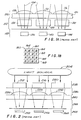
- FIGS. 6A through 6D illustrate cross sections of the microlens structure at various stages in the processing described in FIG. 5.
- the planarized surface 604 is shown with a deposited layer of color microlens resist 608 .
- FIG. 6B illustrates the “square” form of the remaining microlens resist 608 after the patterning block described in block 516 .
- FIG. 6C illustrates the patterned microlens resist during exposure to DUV radiation 612 .
- the color microlens resist is subject to a thermal flow or cross link baking process described in block 524 of FIG. 5 to produce a curved microlens 608 as illustrated in FIG. 6D.
- the color microlens resist which now forms a color microlens of FIG. 6D, is subject to silylated, DUV bleaching and RIE to produce the coated microlens structure 612 illustrated in FIG. 6E.
Landscapes
- Physics & Mathematics (AREA)
- General Physics & Mathematics (AREA)
- Spectroscopy & Molecular Physics (AREA)
- Optics & Photonics (AREA)
- Engineering & Computer Science (AREA)
- Manufacturing & Machinery (AREA)
- Chemical & Material Sciences (AREA)
- Crystallography & Structural Chemistry (AREA)
- Nonlinear Science (AREA)
- Mathematical Physics (AREA)
- Solid State Image Pick-Up Elements (AREA)
Abstract
The making and use of color microlenses in color image sensors and color display devices is described and claimed. The color microlenses combine the function of a colorless microlens and a color filter into a single structure simplifying the fabrication of, and increasing the reliability of display devices and image sensors using the described color microlenses.
Description
- The present invention relates to the field of image sensors and display devices.
- Microlenses have long been used in imaging devices to focus light on sensors including charge couple device (CCD) sensors and complementary metal oxide semiconductor (CMOS) sensors. The microlenses significantly improve the light sensitivity of the imaging device by collecting light from a large light collecting area and focusing it on a small light sensitive area of the sensor. The ratio of the overall light collecting area of a sensor to the light sensitive area of the sensor is defined to be a fill factor. Typical fill factors in prior art designs are less than 50%.
- One prior art method of generating a color image signal is shown in FIG. 1A. Light from a subject to be imaged comes in as
light rays 104 and passes through a set ofmicrolenses planarization layer 120. After passing through theplanarization layer 120, thelight 104 is filtered bycolor filters color filter Typical color filters sensor sensor sensors sensors corresponding color filter sensors sensor red sensor 160,blue sensor 164, green sensor 168) as shown in FIG. 1B, an overall color image can be reconstructed. - The fabrication of separate microlenses, color filters, and image sensors in the structure illustrated in FIGS. 1A and 1B has several disadvantages. For example, one disadvantage of the traditional structure is that many process steps are needed to form a
first layer 148 including thesensors second layer 152 including thecolor filters third planarization layer 156 to supportmicrolenses - Another disadvantage of the current structure is that the
microlenses corresponding image sensors planarization layer 156 and thecolor filter layer 152. The separation reduces the light reaching thesensors multiple layers microlens 112 at an obtuse angle of incidence. The off-axis light passes throughplanarization layers 156 and acolor filter 128 missing thesensor 140 which corresponds to thecolor filter 128 and instead striking anadjacent sensor 136. Alternately, the off-axis light coming in throughmicrolens 112 may pass betweenfilters adjacent sensor 136 resulting in an erroneous readings from theimage sensor 136. - Additional disadvantages of the currect micro-lens filter combinations include the additional process steps being used to fabricate the multi-level structure of FIG. 1, the decreased reliability resulting from separation of
layers transparent microlenses color filters planarization layer 156. - A second use of the microlens, color filter layer, structure is in color display devices. FIG. 2 illustrates an example of using the microlens color filter structure in a thin film transfer (TFT) liquid crystal display device. In FIG. 2, light from a backlight or
other light source 204 passes through acolor filter layer 208 containingcolor filters color filters microlens layer 236 focuses the light fromcorresponding color filters substrate 240 and a liquid crystal display (LCD)layer 244 to aTFT substrate 248. EachTFT switch 252, 256, 260 corresponds to acorresponding color filter switch 252, 256, 260, the output of eachcolor filter - Display devices formed using the described techniques suffer from the previously described disadvantages including (1) difficulty in fabrication; (2) crosstalk between filters and switches caused by the increased separation generated by the microlens layer; and (3) problems with device reliability resulting from adhesion between multiple layers and increased material costs resulting from the necessity for multiple layers.
- Thus an improved method for forming microlens and color filter structures is desired.
- The present invention describes a method of forming a color microlens array on a semiconductor substrate. The method involves depositing a colored microlens resist on a semiconductor surface. The colored microlens resist is patterned and then baked to cause flowing of the colored microlens resist resulting in a color microlens with a curved surface.
- FIG. 1A is a cross section drawing of a conventional color filter array structure for acquiring color images.
- FIG. 1B illustrates an example of an arrangement of color filters in a detection device.
- FIG. 2 is a cross section of a thin film transfer (TFT) based liquid crystal display utilizing a microlens system.
- FIG. 3 illustrates a cross section of a color imaging device for acquiring color images utilizing a colored microlens array which combines microlenses and color filters.
- FIG. 4 is a cross section of a TFT liquid crystal display utilizing the color microlenses of the present invention.
- FIG. 5 shows the processes used in fabricating a colored microlens.
- FIGS. 6A through 6E show the cross-section of a microlens system after key processing operations.
- In the following description, an array of colored microlenses will be described. In the embodiment, the colored microlenses are formed over a planar substrate using semiconductor processing techniques, including photolithography and baking of a microlens resist. Combining the function of a microlens and a color filter into a single colored microlens reduces the number of components and number of operations used to fabricate color display and image acquisition devices. Reducing the number of components also increases device reliability. Examples of devices which utilize color microlenses include, but are not limited to, colored imaging displays, such as TFT displays, for example, and image acquisition devices such as charge coupled device (CCD) digital cameras.
- In the accompanying description, certain details will be provided to facilitate understanding of the invention. For example, certain processes used to form the color microlenses are described. However it is recognized that other methods of fabricating a color microlens may be appropriate. The included details are provided to facilitate understanding of the invention and should not be interpreted to limit the scope of the invention. Certain details will be omitted because such detail would obscure the invention and are already well understood by those of ordinary skill in the art.
- FIG. 3 illustrates a set of
microlenses Light rays 316 from an external source passes through thecolored microlenses sensors microlens microlenses microlens sensor microlens sensors sensors - FIG. 4 illustrates the use of
color microlens light source 416 provides illumination which passes throughmicrolenses counter substrate layer 416 and to a liquid crystal display (LCD)layer 420. Each microlens of a set filters a different color, as well as focuses light from thelight source 416 to a particular region of theLCD crystal layer 420 being switched. The crystals in the LCD under each color microlens act as a switch and filters that light. An applied electric potential determines when light can pass through the liquid crystal in the region underneath the microlens or when light is blocked from passing through theLCD layer 420. Electrodes residing on both sides of theLCD layer 420 are used to apply the electric potential. - In another embodiment, a thin film transfer (TFT)
switch LCD layer 420. The threemicrolenses microlenses - FIG. 5 is a flow diagram illustrating a lithographic method of fabricating color microlenses. In
block 504 the surface of the semiconductor substrate upon which the microlenses will be formed is planarized. Planarization provides a flat and smooth substrate surface upon which a microlens resist can be deposited. In some embodiments, when a surface is already polished and smooth, planarization may be unnecessary. One method of planarization involves spin coating a planarization layer which is subsequently baked. The materials used in the spin coated planarization layer can be classified into either non-photo-definable and photo-definable materials. “Non-photo-definable” materials (non-photo-sensitive materials) include acrylics and polyorganosiloxiane, for example. Examples of “photo-definable” materials (photo-sensitive materials) include acrylic based resists and epoxy based resists. In this embodiment, photo-definable planarization is used because non-photo-definable planarization often requires an extra photolithographic patterning operation to open areas of bond pads, while photo-definable planarization layers can be patterned directly and etched. - In
block 508, a color microlens resist material is deposited on the planarized surface. In one embodiment, deposition of the color microlens resist is achieved by spin coating a planarized layer with the color microlens resist. The thickness of the coating is determined by the required thickness of the microlens. The thickness of the microlens resist is a function of the focal length requirements of the microlens, a shorter focal length requires a thicker lens, and thus, a thicker microlens resist layer. The focal length of the microlens should be designed to effectively focus light on the corresponding sensor. The microlens thickness (t) vs. focus length (f) may be estimated according to the following relationship:
- where:
- A: Area of microlens
- Θ: Contact angle between microlens and supporting substrate
- n 1: refractive index of microlens
- n 0: refractive index of air
- The “contact angle” is a function of the microlens curvature and can be computed as the angle between a first line tangent to the microlens surface at a point on the microlens near the interface between the microlens and the support substrate and a second line parallel to the support substrate surface. The contact angle is illustrated as
angle Θ 450 of FIG. 4. - The thickness and shape of the color microlens may be computed using ray tracing programs and is also dependent on the index of refraction of the microlens resist material. Different colored microlenses may contain different pigments having different indexes of refraction. Thus different microlenses in a set may have different dimensions. In typical sensor applications for which the pixel sizes are around 10 microns by 10 microns, the thickness of the microlens can vary from 2 to 4 microns depending on the index of refraction of the microlens material, the distance of the microlens from the sensor, and the area of the sensor. The determination of lens shapes is well understood in the art and can be computed via commercially available rate tracing programs.
- In
block 512, the microlens resist is baked at a relatively low temperature known as a “soft bake”. In a positive resist, the soft bake process involves baking the microlens resist at a temperature of about 100° Celsius (C.) for a time of approximately one minute. After the soft bake, a patterning process is performed in which the microlens resist is typically exposed to ultraviolet (UV) light in a photolithographic process inblock 516. In one embodiment the UV light has a wavelength or I-line of approximately 365 nanometers and dose of 100 Millijoules/cm2. After exposure to the UV light, the microlens resist is developed in a developer solution. - After the
patterning block 516, the excess microlens resist material is removed leaving the appropriate amount of microlens resist to form a microlens. Typically, the structures remaining have an approximately square form. The square form is fixed using deep ultraviolet exposure, otherwise known as post-patterning flood exposure inblock 520. The deep UV exposure causes cross-linking in the resist improving the transparency of the microlens resist material. - The shape of the microlens after post-patterning flood exposure is still a square form. In block 524, the microlens array is baked at a high temperature to cause the microlens resist to flow and form the desired curved shape. In one implementation of the invention, the microlens array is heated to a temperature of approximately 150° C. for a predetermined period of time (e.g., approximately two minutes).
-
Blocks 508 through 524 are repeated for each different colored microlens to be deposited on a planarized surface. Thus if a red, green and blue microlens are to be formed on the planarized surface, three iterations of the operations set forth inblocks 508 through 524 are typically required, one iteration for the red microlens, a second iteration for the green microlens and a third iteration for the blue microlens. When inblock 528, it is determined that the last microlens has been formed on the planarized surface, an optional silylating layer is formed over the microlenses inblock 532. - Typically, the microlens array, formed in accordance with
block 504 through 524, is a polymeric lens array and is formed from photoresists. However, prior to silylation, these polymeric microlenses formed from photo resists lack the mechanical, thermal and environmental stability required for most devices. Thus, in this embodiment, the surface of the microlens array is silicated through silylation of the microlens resist. This silicated process is known to stabilize the resist and is described in literature such as Introduction to Microlithography edited by L. Thompson, C. Grant Wilson, and M. J. Bowden published by The American Chemical Society copyrighted 1994. On pages 243 to 244. - In one embodiment of the invention, the silylated microlens are further subject to deep ultraviolet bleaching. In the bleaching process, the microlens array is exposed to Deep (DUV) radiation of approximately 200-300 nanometers and intensity of 500 milliWatts/centimeter 2 wavelength for a period of one minute time such as that which occurs in Fusion DUV systems. The UV bleaching changes the light transmittance characteristics of the color microlenses. Bleaching reduces the tendency of the microlenses to have a yellowish tint.
- In block 540, the silylated color microlens surface is converted to a silicated surface using an oxygen reactive ion treatment (RIE). A silicated surface is preferred to the salyated surface because the silicated surface is stiffer, more stable and resistant to deformation. In order to convert the salyated surface to a silicated surface, the salyated microlens surface is exposed to an oxygen reactive ion etch for approximately 30 seconds. The RIE etch power should be low enough such that it does not cause significant etching. A typical RIE etch power may be approximately 60 watts.
- FIGS. 6A through 6D illustrate cross sections of the microlens structure at various stages in the processing described in FIG. 5. In FIG. 6A, the
planarized surface 604 is shown with a deposited layer of color microlens resist 608. FIG. 6B illustrates the “square” form of the remaining microlens resist 608 after the patterning block described inblock 516. FIG. 6C illustrates the patterned microlens resist during exposure toDUV radiation 612. In order to round angular edges, the color microlens resist is subject to a thermal flow or cross link baking process described in block 524 of FIG. 5 to produce acurved microlens 608 as illustrated in FIG. 6D. The color microlens resist, which now forms a color microlens of FIG. 6D, is subject to silylated, DUV bleaching and RIE to produce thecoated microlens structure 612 illustrated in FIG. 6E. - While certain exemplary embodiments have been described in detail and shown in the accompanying drawings and description, it is to be understood that such embodiments are merely illustrative and not restrictive on the broad invention. This invention is not to be limited to the specific arrangement and constructions shown and described; since various other modifications may occur to those of ordinary skill in the art.
Claims (17)
1. A method of forming a color microlens array on a semiconductor structure comprising:
depositing a first colored microlens resist on a semiconductor surface;
patterning the first colored microlens resist; and
baking the first colored microlens resist to cause flowing of the first colored microlens resist resulting in at least one microlens with a curved surface.
2. The method of further comprising:
claim 1
fixing the first colored microlens resist by deep ultra-violet exposure to cause cross-linking in the microlens resist after the patterning of the colored microlens resist.
3. The method of further comprising:
claim 1
stabilizing the microlens surface using silylation of a surface of the first colored microlens.
4. The method of further comprising repeating the depositing, patterning and baking operations on said semiconductor structure using a second colored microlens resist, said second microlens resist filtering a different color than said first colored microlens resist.
claim 1
5. The method of further comprising:
claim 1
exposing at least one microlens to a deep ultra-violet bleaching to improve transparency.
6. The method of wherein the depositing, patterning, and baking operations are repeated three times, each time corresponding to a different colored polymer resist.
claim 1
7. The method of wherein the patterning operation is performed using a photolithographic process.
claim 1
8. A color imaging acquisition device comprising:
an array of light sensitive sensors; and
an array of color microlenses, each microlens in the array of color microlenses corresponding to a light sensitive sensor in the array of light sensitive sensors and designed to filter a corresponding color of light.
9. The color image acquisition device of :
claim 8
wherein each microlens in the array of color microlens is an element in a corresponding set of microlenses, each microlens in each set filtering a different color of light.
10. The color image acquisition device of wherein each microlens in the array of color microlenses is less than 15 microns in diameter.
claim 8
11. The color acquisition device of wherein the light sensitive sensors are charge coupled device sensors.
claim 8
12. The color acquisition device of wherein the light sensitive sensors are metal oxide semiconductor sensors.
claim 8
13. The color acquisition device of wherein a microlens of the array of the color microlenses is formed from a pigmented polymer.
claim 8
14. A color display device comprising:
a light source;
a plurality of switches for-controlling light from the light source; and
a plurality of color microlens for focusing and filtering light from the light source and delivering the light from the light source to the plurality of switches.
15. The color display device of wherein each switch of said plurality of switches is a region of a liquid crystal display layer.
claim 14
16. The color display device of wherein each microlens in said plurality of color microlenses corresponds to a switch in said plurality of switches.
claim 14
17. The color display device of wherein the plurality of color microlenses are organized into multiple sets of color microlens, each set of color microlenses including three microlenses from the plurality of color microlenses, each microlens in the set of microlenses for filtering a different colored light.
claim 14
Priority Applications (2)
| Application Number | Priority Date | Filing Date | Title |
|---|---|---|---|
| US09/902,012 US6433844B2 (en) | 1998-03-31 | 2001-07-09 | Method for creating a color microlens array of a color display layer |
| US10/185,777 US20020176037A1 (en) | 1998-03-31 | 2002-06-27 | Method for creating a color microlens |
Applications Claiming Priority (2)
| Application Number | Priority Date | Filing Date | Title |
|---|---|---|---|
| US09/052,609 US6271900B1 (en) | 1998-03-31 | 1998-03-31 | Integrated microlens and color filter structure |
| US09/902,012 US6433844B2 (en) | 1998-03-31 | 2001-07-09 | Method for creating a color microlens array of a color display layer |
Related Parent Applications (1)
| Application Number | Title | Priority Date | Filing Date |
|---|---|---|---|
| US09/052,609 Division US6271900B1 (en) | 1998-03-31 | 1998-03-31 | Integrated microlens and color filter structure |
Related Child Applications (1)
| Application Number | Title | Priority Date | Filing Date |
|---|---|---|---|
| US10/185,777 Division US20020176037A1 (en) | 1998-03-31 | 2002-06-27 | Method for creating a color microlens |
Publications (2)
| Publication Number | Publication Date |
|---|---|
| US20010050737A1 true US20010050737A1 (en) | 2001-12-13 |
| US6433844B2 US6433844B2 (en) | 2002-08-13 |
Family
ID=21978725
Family Applications (3)
| Application Number | Title | Priority Date | Filing Date |
|---|---|---|---|
| US09/052,609 Expired - Fee Related US6271900B1 (en) | 1998-03-31 | 1998-03-31 | Integrated microlens and color filter structure |
| US09/902,012 Expired - Fee Related US6433844B2 (en) | 1998-03-31 | 2001-07-09 | Method for creating a color microlens array of a color display layer |
| US10/185,777 Abandoned US20020176037A1 (en) | 1998-03-31 | 2002-06-27 | Method for creating a color microlens |
Family Applications Before (1)
| Application Number | Title | Priority Date | Filing Date |
|---|---|---|---|
| US09/052,609 Expired - Fee Related US6271900B1 (en) | 1998-03-31 | 1998-03-31 | Integrated microlens and color filter structure |
Family Applications After (1)
| Application Number | Title | Priority Date | Filing Date |
|---|---|---|---|
| US10/185,777 Abandoned US20020176037A1 (en) | 1998-03-31 | 2002-06-27 | Method for creating a color microlens |
Country Status (4)
| Country | Link |
|---|---|
| US (3) | US6271900B1 (en) |
| AU (1) | AU3083999A (en) |
| TW (1) | TW417309B (en) |
| WO (1) | WO1999050914A1 (en) |
Cited By (5)
| Publication number | Priority date | Publication date | Assignee | Title |
|---|---|---|---|---|
| US6738171B1 (en) * | 2001-11-21 | 2004-05-18 | Micron Technology, Inc. | Color filter array and microlens array having holographic optical elements |
| US20040223071A1 (en) * | 2003-05-08 | 2004-11-11 | David Wells | Multiple microlens system for image sensors or display units |
| US20050133688A1 (en) * | 2003-12-22 | 2005-06-23 | Jin Li | Layered lens structures and methods of production |
| US20050161841A1 (en) * | 2001-07-26 | 2005-07-28 | Bolle Cristian A. | Method for making micro lenses |
| JP2015031941A (en) * | 2013-08-07 | 2015-02-16 | セイコーエプソン株式会社 | Electro-optical device, method of manufacturing electro-optical device, and electronic apparatus |
Families Citing this family (99)
| Publication number | Priority date | Publication date | Assignee | Title |
|---|---|---|---|---|
| KR100213968B1 (en) | 1996-07-15 | 1999-08-02 | 구자홍 | LCD Display |
| US6083429A (en) * | 1998-03-31 | 2000-07-04 | Intel Corporation | Microlens formation through focal plane control of a aerial image |
| US6271900B1 (en) * | 1998-03-31 | 2001-08-07 | Intel Corporation | Integrated microlens and color filter structure |
| JP2000029011A (en) * | 1998-07-14 | 2000-01-28 | Seiko Epson Corp | Electro-optical device, manufacturing method thereof, and projection display device |
| JP3824042B2 (en) * | 1998-12-10 | 2006-09-20 | セイコーエプソン株式会社 | Optical substrate, manufacturing method thereof, and display device |
| US6297540B1 (en) * | 1999-06-03 | 2001-10-02 | Intel Corporation | Microlens for surface mount products |
| JP5020428B2 (en) * | 1999-08-30 | 2012-09-05 | 三星電子株式会社 | Top gate polysilicon thin film transistor manufacturing method |
| EP1269129A1 (en) * | 2000-03-29 | 2003-01-02 | Siemens Aktiengesellschaft | Thermal radiation detection device, method for producing the same and use of said device |
| US6301051B1 (en) * | 2000-04-05 | 2001-10-09 | Rockwell Technologies, Llc | High fill-factor microlens array and fabrication method |
| JP3840058B2 (en) * | 2000-04-07 | 2006-11-01 | キヤノン株式会社 | Microlens, solid-state imaging device and manufacturing method thereof |
| US7092165B2 (en) | 2000-07-31 | 2006-08-15 | Corning Incorporated | Microlens arrays having high focusing efficiency |
| EP1305656A4 (en) * | 2000-07-31 | 2006-03-08 | Rochester Photonics Corp | Structure screens for controlled spreading of light |
| TW526395B (en) * | 2000-09-29 | 2003-04-01 | United Microelectronics Corp | Method to improve side profile of photoresist pattern |
| US7139028B2 (en) * | 2000-10-17 | 2006-11-21 | Canon Kabushiki Kaisha | Image pickup apparatus |
| DE60134950D1 (en) * | 2001-02-08 | 2008-09-04 | Sgs Thomson Microelectronics | Reference data encoding for a solid-state imaging device |
| EP1365383B1 (en) | 2002-05-23 | 2011-06-22 | Nokia Corporation | Method and device for determining the lighting conditions surrounding a LCD color display device for correcting its chrominance |
| US20040012708A1 (en) * | 2002-07-18 | 2004-01-22 | Matherson Kevin James | Optical prefilter system that provides variable blur |
| TW588195B (en) * | 2002-07-30 | 2004-05-21 | Hong-Da Liu | Reflector structure in a liquid crystal display having light condensing effect |
| US20040041965A1 (en) * | 2002-09-04 | 2004-03-04 | Hong-Da Liu | Transflector with a high gain of light efficiency for a liquid crystal display |
| JP2004111867A (en) | 2002-09-20 | 2004-04-08 | Canon Inc | Solid-state imaging device |
| US6608358B1 (en) * | 2002-10-25 | 2003-08-19 | Hua Wei Semiconductor (Shanghai) Co., Ltd. | Dummy pattern for improving micro-lens formation in an image sensor |
| US6818962B2 (en) * | 2002-10-25 | 2004-11-16 | Omnivision International Holding Ltd | Image sensor having integrated thin film infrared filter |
| US6861280B2 (en) * | 2002-10-25 | 2005-03-01 | Omnivision International Holding Ltd | Image sensor having micro-lenses with integrated color filter and method of making |
| US6638786B2 (en) * | 2002-10-25 | 2003-10-28 | Hua Wei Semiconductor (Shanghai ) Co., Ltd. | Image sensor having large micro-lenses at the peripheral regions |
| JP3796499B2 (en) * | 2002-11-06 | 2006-07-12 | キヤノン株式会社 | Color display element, color display element driving method, and color display device |
| US7001795B2 (en) * | 2003-02-27 | 2006-02-21 | Micron Technology, Inc. | Total internal reflection (TIR) CMOS imager |
| US7502058B2 (en) * | 2003-06-09 | 2009-03-10 | Micron Technology, Inc. | Imager with tuned color filter |
| EP1500975A3 (en) * | 2003-07-21 | 2006-01-18 | Ingeneric GmbH | Process for the fabrication of optical microstructures |
| US20050062928A1 (en) * | 2003-09-24 | 2005-03-24 | Po-Hung Yau | Differactive micro-structure color wavelength division device |
| US7227692B2 (en) * | 2003-10-09 | 2007-06-05 | Micron Technology, Inc | Method and apparatus for balancing color response of imagers |
| US7307788B2 (en) * | 2004-12-03 | 2007-12-11 | Micron Technology, Inc. | Gapless microlens array and method of fabrication |
| US7199931B2 (en) * | 2003-10-09 | 2007-04-03 | Micron Technology, Inc. | Gapless microlens array and method of fabrication |
| US7476562B2 (en) * | 2003-10-09 | 2009-01-13 | Aptina Imaging Corporation | Gapless microlens array and method of fabrication |
| US7560295B2 (en) * | 2003-10-09 | 2009-07-14 | Aptina Imaging Corporation | Methods for creating gapless inner microlenses, arrays of microlenses, and imagers having same |
| US20050122291A1 (en) * | 2003-12-04 | 2005-06-09 | May Gregory J. | Optically addressable pixel and receptacle array |
| GB0401462D0 (en) * | 2004-01-23 | 2004-02-25 | Melexis Nv | Digital imaging device |
| US8654815B1 (en) | 2004-04-02 | 2014-02-18 | Rearden, Llc | System and method for distributed antenna wireless communications |
| US9826537B2 (en) | 2004-04-02 | 2017-11-21 | Rearden, Llc | System and method for managing inter-cluster handoff of clients which traverse multiple DIDO clusters |
| US9819403B2 (en) | 2004-04-02 | 2017-11-14 | Rearden, Llc | System and method for managing handoff of a client between different distributed-input-distributed-output (DIDO) networks based on detected velocity of the client |
| US10425134B2 (en) | 2004-04-02 | 2019-09-24 | Rearden, Llc | System and methods for planned evolution and obsolescence of multiuser spectrum |
| US20050274871A1 (en) | 2004-06-10 | 2005-12-15 | Jin Li | Method and apparatus for collecting photons in a solid state imaging sensor |
| US7068432B2 (en) * | 2004-07-27 | 2006-06-27 | Micron Technology, Inc. | Controlling lens shape in a microlens array |
| JP4546797B2 (en) * | 2004-09-24 | 2010-09-15 | パナソニック株式会社 | Solid-state imaging device, manufacturing method thereof, and camera |
| KR20060077709A (en) * | 2004-12-30 | 2006-07-05 | 동부일렉트로닉스 주식회사 | CMOS image sensor |
| US10148897B2 (en) * | 2005-07-20 | 2018-12-04 | Rearden, Llc | Apparatus and method for capturing still images and video using coded lens imaging techniques |
| JP2007033597A (en) * | 2005-07-25 | 2007-02-08 | Seiko Epson Corp | Optical sheet, backlight unit, electro-optical device, electronic apparatus, optical sheet manufacturing method, and optical sheet cutting method |
| KR100731133B1 (en) * | 2005-12-29 | 2007-06-22 | 동부일렉트로닉스 주식회사 | Manufacturing Method of CMOS Image Sensor |
| US20070242191A1 (en) * | 2006-04-04 | 2007-10-18 | Po-Hung Yau | Micro-structure color wavelenght division device |
| US8610806B2 (en) | 2006-08-28 | 2013-12-17 | Micron Technology, Inc. | Color filter array, imagers and systems having same, and methods of fabrication and use thereof |
| JP2008091841A (en) * | 2006-10-05 | 2008-04-17 | Sony Corp | Solid-state imaging device and imaging device |
| CN101558331B (en) * | 2006-12-14 | 2011-07-27 | 松下电器产业株式会社 | Lens and method for manufacturing the same |
| US7687776B2 (en) * | 2007-04-11 | 2010-03-30 | General Monitors, Inc. | Gas and/or flame imaging system with explosion proof housing |
| KR20080101190A (en) * | 2007-05-16 | 2008-11-21 | 주식회사 동부하이텍 | Manufacturing Method of Image Sensor |
| JP4576412B2 (en) * | 2007-09-05 | 2010-11-10 | シャープ株式会社 | Manufacturing method of colored microlens array, color solid-state imaging device and manufacturing method thereof, manufacturing method of color display device, manufacturing method of electronic information device |
| KR20090061310A (en) * | 2007-12-11 | 2009-06-16 | 주식회사 동부하이텍 | Image sensor and its manufacturing method |
| DE102008043621A1 (en) | 2008-11-10 | 2010-05-12 | Seereal Technologies S.A. | Holographic color display |
| JP5320270B2 (en) * | 2009-11-25 | 2013-10-23 | 株式会社沖データ | Manufacturing method of display panel |
| CN102544390B (en) * | 2010-12-07 | 2015-03-25 | 群康科技(深圳)有限公司 | Manufacturing method of micro-lens structure and image display system comprising micro-lens structure |
| US8755121B2 (en) | 2011-01-28 | 2014-06-17 | Crane & Co., Inc. | Laser marked device |
| US8466000B2 (en) | 2011-04-14 | 2013-06-18 | United Microelectronics Corp. | Backside-illuminated image sensor and fabricating method thereof |
| US20130010165A1 (en) | 2011-07-05 | 2013-01-10 | United Microelectronics Corp. | Optical micro structure, method for fabricating the same and applications thereof |
| RU2641316C9 (en) | 2011-08-19 | 2019-03-21 | Визуал Физикс, Ллс | Optionally transferable optical system with reduced thickness |
| US9312292B2 (en) | 2011-10-26 | 2016-04-12 | United Microelectronics Corp. | Back side illumination image sensor and manufacturing method thereof |
| US8318579B1 (en) | 2011-12-01 | 2012-11-27 | United Microelectronics Corp. | Method for fabricating semiconductor device |
| US8815102B2 (en) | 2012-03-23 | 2014-08-26 | United Microelectronics Corporation | Method for fabricating patterned dichroic film |
| US9401441B2 (en) | 2012-06-14 | 2016-07-26 | United Microelectronics Corporation | Back-illuminated image sensor with dishing depression surface |
| CN102693995B (en) * | 2012-06-20 | 2015-06-03 | 中国科学院上海高等研究院 | Image Sensor |
| US8779344B2 (en) | 2012-07-11 | 2014-07-15 | United Microelectronics Corp. | Image sensor including a deep trench isolation (DTI)that does not contact a connecting element physically |
| CA2881826C (en) | 2012-08-17 | 2021-03-30 | Visual Physics, Llc | A process for transferring microstructures to a final substrate |
| US8828779B2 (en) | 2012-11-01 | 2014-09-09 | United Microelectronics Corp. | Backside illumination (BSI) CMOS image sensor process |
| US11189917B2 (en) | 2014-04-16 | 2021-11-30 | Rearden, Llc | Systems and methods for distributing radioheads |
| US8779484B2 (en) | 2012-11-29 | 2014-07-15 | United Microelectronics Corp. | Image sensor and process thereof |
| US9973246B2 (en) | 2013-03-12 | 2018-05-15 | Rearden, Llc | Systems and methods for exploiting inter-cell multiplexing gain in wireless cellular systems via distributed input distributed output technology |
| US9923657B2 (en) | 2013-03-12 | 2018-03-20 | Rearden, Llc | Systems and methods for exploiting inter-cell multiplexing gain in wireless cellular systems via distributed input distributed output technology |
| US10488535B2 (en) | 2013-03-12 | 2019-11-26 | Rearden, Llc | Apparatus and method for capturing still images and video using diffraction coded imaging techniques |
| US10547358B2 (en) | 2013-03-15 | 2020-01-28 | Rearden, Llc | Systems and methods for radio frequency calibration exploiting channel reciprocity in distributed input distributed output wireless communications |
| JP6410793B2 (en) | 2013-03-15 | 2018-10-24 | ビジュアル フィジクス エルエルシー | Optical security device |
| US9279923B2 (en) | 2013-03-26 | 2016-03-08 | United Microelectronics Corporation | Color filter layer and method of fabricating the same |
| US9537040B2 (en) | 2013-05-09 | 2017-01-03 | United Microelectronics Corp. | Complementary metal-oxide-semiconductor image sensor and manufacturing method thereof |
| US9129876B2 (en) | 2013-05-28 | 2015-09-08 | United Microelectronics Corp. | Image sensor and process thereof |
| US9873281B2 (en) | 2013-06-13 | 2018-01-23 | Visual Physics, Llc | Single layer image projection film |
| US9709488B2 (en) * | 2013-09-12 | 2017-07-18 | Nec Corporation | Sensor unit |
| US9823128B2 (en) * | 2013-10-16 | 2017-11-21 | Arizona Board Of Regents On Behalf Of The University Of Arizona | Multispectral imaging based on computational imaging and a narrow-band absorptive filter array |
| US9054106B2 (en) | 2013-11-13 | 2015-06-09 | United Microelectronics Corp. | Semiconductor structure and method for manufacturing the same |
| US9841319B2 (en) | 2013-11-19 | 2017-12-12 | United Microelectronics Corp. | Light detecting device |
| US10434812B2 (en) | 2014-03-27 | 2019-10-08 | Visual Physics, Llc | Optical device that produces flicker-like optical effects |
| US10766292B2 (en) | 2014-03-27 | 2020-09-08 | Crane & Co., Inc. | Optical device that provides flicker-like optical effects |
| EP4582263A1 (en) | 2014-07-17 | 2025-07-09 | Visual Physics, LLC | An improved polymeric sheet material for use in making polymeric security documents such as banknotes |
| US9465175B2 (en) * | 2014-07-23 | 2016-10-11 | Sifotonics Technologies Co., Ltd. | Integrated lens-array-on-substrate for optical coupling system and fabrication method thereof |
| MX391783B (en) | 2014-09-16 | 2025-03-21 | Crane Security Tech Inc | SAFETY LENS COAT. |
| CA2976218C (en) | 2015-02-11 | 2023-02-14 | Crane & Co., Inc. | Method for the surface application of a security device to a substrate |
| US10684491B2 (en) | 2015-10-02 | 2020-06-16 | Pure Depth Limited | Method and system using refractive beam mapper having square element profiles to reduce moire interference in a display system including multiple displays |
| RU2705440C1 (en) | 2015-10-02 | 2019-11-07 | Эптив Текнолоджиз Лимитед | Method and system for making color filter offsets to reduce moiré interference in a display system including a plurality of displays |
| KR20180101321A (en) | 2015-10-02 | 2018-09-12 | 푸에뎁스 리미티드 | Method and system for using a refractive beam mapper to reduce moire interference in a display system including multiple displays |
| EP3365723B1 (en) | 2015-10-02 | 2021-12-22 | Aptiv Technologies Limited | Method and system for performing sub-pixel compression in order to reduce moiré interference in a display system including multiple displays |
| CN106384744B (en) * | 2016-11-16 | 2020-04-03 | 信利(惠州)智能显示有限公司 | Method for manufacturing organic light emitting display device |
| EP3580067B1 (en) | 2017-02-10 | 2022-04-06 | Crane & Co., Inc. | Machine-readable optical security device |
| US10522579B2 (en) | 2017-11-15 | 2019-12-31 | Taiwan Semiconductor Manufacturing Co., Ltd. | Light blocking layer for image sensor device |
| KR102260151B1 (en) * | 2019-11-13 | 2021-06-07 | (주)에이앤아이 | High-Sensitive Contactless Device of Color Meter |
Family Cites Families (18)
| Publication number | Priority date | Publication date | Assignee | Title |
|---|---|---|---|---|
| JPS614020A (en) * | 1984-06-18 | 1986-01-09 | Nissha Printing Co Ltd | Multicolor liquid crystal display device |
| JP3067114B2 (en) * | 1991-06-04 | 2000-07-17 | ソニー株式会社 | Micro lens formation method |
| JPH05167054A (en) * | 1991-12-19 | 1993-07-02 | Toshiba Corp | Manufacture of solid-state image sensing device |
| JP2566087B2 (en) * | 1992-01-27 | 1996-12-25 | 株式会社東芝 | Colored microlens array and manufacturing method thereof |
| US5418635A (en) * | 1992-02-19 | 1995-05-23 | Sharp Kabushiki Kaisha | Liquid crystal device with a reflective substrate with bumps of photosensitive resin which have 2 or more heights and random configuration |
| JPH06244392A (en) * | 1993-02-17 | 1994-09-02 | Sharp Corp | Solid-state imaging device and manufacturing method thereof |
| US5766980A (en) * | 1994-03-25 | 1998-06-16 | Matsushita Electronics Corporation | Method of manufacturing a solid state imaging device |
| JPH08179300A (en) | 1994-12-22 | 1996-07-12 | Sony Corp | Color display |
| US5739548A (en) * | 1995-05-02 | 1998-04-14 | Matsushita Electronics Corporation | Solid state imaging device having a flattening layer and optical lenses |
| US5677200A (en) | 1995-05-12 | 1997-10-14 | Lg Semicond Co., Ltd. | Color charge-coupled device and method of manufacturing the same |
| US5723264A (en) * | 1996-03-14 | 1998-03-03 | Eastman Kodak Company | Pattern transfer techniques for fabrication of lenslet arrays using specialized polyesters |
| KR100190855B1 (en) * | 1995-12-22 | 1999-06-01 | 윤종용 | LCD color filter and manufacturing method thereof |
| SG63687A1 (en) * | 1996-01-10 | 1999-03-30 | Sumitomo Chemical Co | A microlens-array production method thereof and liquid crystal display device using the same |
| US5718830A (en) * | 1996-02-15 | 1998-02-17 | Lucent Technologies Inc. | Method for making microlenses |
| US5948281A (en) * | 1996-08-30 | 1999-09-07 | Sony Corporation | Microlens array and method of forming same and solid-state image pickup device and method of manufacturing same |
| US6271900B1 (en) * | 1998-03-31 | 2001-08-07 | Intel Corporation | Integrated microlens and color filter structure |
| US6297911B1 (en) * | 1998-08-27 | 2001-10-02 | Seiko Epson Corporation | Micro lens array, method of fabricating the same, and display device |
| US6171833B1 (en) * | 1998-12-23 | 2001-01-09 | Massachusetts Institute Of Technology | Pyruvate carboxylase from corynebacterium glutamicum |
-
1998
- 1998-03-31 US US09/052,609 patent/US6271900B1/en not_active Expired - Fee Related
-
1999
- 1999-03-12 WO PCT/US1999/005439 patent/WO1999050914A1/en not_active Ceased
- 1999-03-12 AU AU30839/99A patent/AU3083999A/en not_active Abandoned
- 1999-03-31 TW TW088105068A patent/TW417309B/en not_active IP Right Cessation
-
2001
- 2001-07-09 US US09/902,012 patent/US6433844B2/en not_active Expired - Fee Related
-
2002
- 2002-06-27 US US10/185,777 patent/US20020176037A1/en not_active Abandoned
Cited By (15)
| Publication number | Priority date | Publication date | Assignee | Title |
|---|---|---|---|---|
| US20050161841A1 (en) * | 2001-07-26 | 2005-07-28 | Bolle Cristian A. | Method for making micro lenses |
| US6738171B1 (en) * | 2001-11-21 | 2004-05-18 | Micron Technology, Inc. | Color filter array and microlens array having holographic optical elements |
| US20040223071A1 (en) * | 2003-05-08 | 2004-11-11 | David Wells | Multiple microlens system for image sensors or display units |
| WO2004102675A3 (en) * | 2003-05-08 | 2005-02-24 | Micron Technology Inc | Multiple microlens system for image sensors or display units |
| US7916204B2 (en) | 2003-05-08 | 2011-03-29 | Micron Technology, Inc. | Multiple microlens system for image sensors or display |
| US20100073540A1 (en) * | 2003-05-08 | 2010-03-25 | David Wells | Multiple microlens system for image sensors or display units |
| US20060289723A1 (en) * | 2003-12-22 | 2006-12-28 | Jin Li | Layered microlens structures and devices |
| US7199347B2 (en) | 2003-12-22 | 2007-04-03 | Micron Technology, Inc. | Layered microlens structures and devices |
| US7205526B2 (en) | 2003-12-22 | 2007-04-17 | Micron Technology, Inc. | Methods of fabricating layered lens structures |
| US20070096016A1 (en) * | 2003-12-22 | 2007-05-03 | Jin Li | Layered lens structures and methods of production |
| US7365305B2 (en) | 2003-12-22 | 2008-04-29 | Micron Technology, Inc. | Layered lens structures and methods of production in which radius of curvature of the upper lens can be varied |
| US20060027734A1 (en) * | 2003-12-22 | 2006-02-09 | Jin Li | Layered microlens structures and devices |
| US20050133688A1 (en) * | 2003-12-22 | 2005-06-23 | Jin Li | Layered lens structures and methods of production |
| US20110180695A1 (en) * | 2003-12-22 | 2011-07-28 | Round Rock Research, Llc | Layered lens structures and methods of production |
| JP2015031941A (en) * | 2013-08-07 | 2015-02-16 | セイコーエプソン株式会社 | Electro-optical device, method of manufacturing electro-optical device, and electronic apparatus |
Also Published As
| Publication number | Publication date |
|---|---|
| US6271900B1 (en) | 2001-08-07 |
| US6433844B2 (en) | 2002-08-13 |
| AU3083999A (en) | 1999-10-18 |
| TW417309B (en) | 2001-01-01 |
| WO1999050914A1 (en) | 1999-10-07 |
| US20020176037A1 (en) | 2002-11-28 |
Similar Documents
| Publication | Publication Date | Title |
|---|---|---|
| US6271900B1 (en) | Integrated microlens and color filter structure | |
| EP1458028B1 (en) | Solid-state image sensor and production method of the same | |
| RU2426195C1 (en) | Photoelectric converter, imaging system | |
| WO2013121742A1 (en) | Image pickup element | |
| US7829965B2 (en) | Touching microlens structure for a pixel sensor and method of fabrication | |
| JPH04206966A (en) | Production of solid-state image pick up element | |
| JPH0645569A (en) | Solid-state imaging device and manufacturing method thereof | |
| TWI251340B (en) | A solid-state image sensor and a manufacturing method thereof | |
| JP4998310B2 (en) | Solid-state imaging device and imaging apparatus using the same | |
| EP4088917A1 (en) | Micro lens arrays and methods of formation thereof | |
| US20200075651A1 (en) | Double-layer color filter and method for forming the same | |
| JP3538382B2 (en) | Ultra-compact collector for photosensitive devices | |
| JP2000357786A (en) | Solid-state imaging device | |
| JPH06140612A (en) | Imaging device and imaging device | |
| JP2010171450A (en) | Solid-state image sensor and digital camera | |
| JP2007053318A (en) | Solid-state imaging device and manufacturing method thereof | |
| JPH01270362A (en) | Solid-state image sensing device and manufacture thereof | |
| JP2004335598A (en) | Solid-state imaging device and method of manufacturing the same | |
| JP2723686B2 (en) | Solid-state imaging device and method of manufacturing the same | |
| CN120813083B (en) | Image sensors and their fabrication methods, electronic devices | |
| JP2003209231A (en) | Solid-state imaging device and solid-state imaging system | |
| JP2000183321A (en) | Solid-state imaging device and method of manufacturing the same | |
| JPH0653457A (en) | Solid state color image sensor | |
| TWI233984B (en) | Image sensor having micro-lens array separated with ridge structures and method of making | |
| JPH0943427A (en) | Light-collecting filter and manufacturing method thereof |
Legal Events
| Date | Code | Title | Description |
|---|---|---|---|
| CC | Certificate of correction | ||
| FPAY | Fee payment |
Year of fee payment: 4 |
|
| REMI | Maintenance fee reminder mailed | ||
| LAPS | Lapse for failure to pay maintenance fees | ||
| STCH | Information on status: patent discontinuation |
Free format text: PATENT EXPIRED DUE TO NONPAYMENT OF MAINTENANCE FEES UNDER 37 CFR 1.362 |
|
| FP | Lapsed due to failure to pay maintenance fee |
Effective date: 20100813 |