US12171094B2 - Semiconductor structure, formation method thereof and memory - Google Patents
Semiconductor structure, formation method thereof and memory Download PDFInfo
- Publication number
- US12171094B2 US12171094B2 US17/486,696 US202117486696A US12171094B2 US 12171094 B2 US12171094 B2 US 12171094B2 US 202117486696 A US202117486696 A US 202117486696A US 12171094 B2 US12171094 B2 US 12171094B2
- Authority
- US
- United States
- Prior art keywords
- channel
- convex portion
- sacrificial layer
- layer
- sidewall
- Prior art date
- Legal status (The legal status is an assumption and is not a legal conclusion. Google has not performed a legal analysis and makes no representation as to the accuracy of the status listed.)
- Active, expires
Links
Images


Classifications
-
- H—ELECTRICITY
- H10—SEMICONDUCTOR DEVICES; ELECTRIC SOLID-STATE DEVICES NOT OTHERWISE PROVIDED FOR
- H10B—ELECTRONIC MEMORY DEVICES
- H10B12/00—Dynamic random access memory [DRAM] devices
- H10B12/30—DRAM devices comprising one-transistor - one-capacitor [1T-1C] memory cells
- H10B12/34—DRAM devices comprising one-transistor - one-capacitor [1T-1C] memory cells the transistor being at least partially in a trench in the substrate
-
- H—ELECTRICITY
- H10—SEMICONDUCTOR DEVICES; ELECTRIC SOLID-STATE DEVICES NOT OTHERWISE PROVIDED FOR
- H10B—ELECTRONIC MEMORY DEVICES
- H10B12/00—Dynamic random access memory [DRAM] devices
- H10B12/01—Manufacture or treatment
- H10B12/02—Manufacture or treatment for one transistor one-capacitor [1T-1C] memory cells
- H10B12/05—Making the transistor
- H10B12/053—Making the transistor the transistor being at least partially in a trench in the substrate
-
- H—ELECTRICITY
- H10—SEMICONDUCTOR DEVICES; ELECTRIC SOLID-STATE DEVICES NOT OTHERWISE PROVIDED FOR
- H10D—INORGANIC ELECTRIC SEMICONDUCTOR DEVICES
- H10D30/00—Field-effect transistors [FET]
- H10D30/60—Insulated-gate field-effect transistors [IGFET]
- H10D30/63—Vertical IGFETs
-
- H—ELECTRICITY
- H10—SEMICONDUCTOR DEVICES; ELECTRIC SOLID-STATE DEVICES NOT OTHERWISE PROVIDED FOR
- H10D—INORGANIC ELECTRIC SEMICONDUCTOR DEVICES
- H10D62/00—Semiconductor bodies, or regions thereof, of devices having potential barriers
- H10D62/10—Shapes, relative sizes or dispositions of the regions of the semiconductor bodies; Shapes of the semiconductor bodies
- H10D62/17—Semiconductor regions connected to electrodes not carrying current to be rectified, amplified or switched, e.g. channel regions
- H10D62/213—Channel regions of field-effect devices
- H10D62/221—Channel regions of field-effect devices of FETs
- H10D62/235—Channel regions of field-effect devices of FETs of IGFETs
- H10D62/292—Non-planar channels of IGFETs
-
- H—ELECTRICITY
- H10—SEMICONDUCTOR DEVICES; ELECTRIC SOLID-STATE DEVICES NOT OTHERWISE PROVIDED FOR
- H10D—INORGANIC ELECTRIC SEMICONDUCTOR DEVICES
- H10D64/00—Electrodes of devices having potential barriers
- H10D64/20—Electrodes characterised by their shapes, relative sizes or dispositions
- H10D64/27—Electrodes not carrying the current to be rectified, amplified, oscillated or switched, e.g. gates
- H10D64/311—Gate electrodes for field-effect devices
- H10D64/411—Gate electrodes for field-effect devices for FETs
- H10D64/511—Gate electrodes for field-effect devices for FETs for IGFETs
- H10D64/512—Disposition of the gate electrodes, e.g. buried gates
- H10D64/513—Disposition of the gate electrodes, e.g. buried gates within recesses in the substrate, e.g. trench gates, groove gates or buried gates
Definitions
- the present application relates to the field of semiconductor technologies, and in particular, to a semiconductor structure, a formation method thereof and a memory.
- the background described in the present application belongs to technologies related to the present application, and is intended to only illustrate and facilitate the understanding of the application content of the present application.
- the background should not be understood as the prior art relative to a filing date of the present application when the present application is filed for the first time, which is definitely confirmed by the applicant or is inferred to be confirmed by the applicant.
- a Dynamic Random Access Memory is a semiconductor memory widely used in mobile phones, computers, automobiles and other electronic products.
- the difficulty of a DRAM process is related to a size. The smaller the size, the greater the difficulty. In the future, a DRAM process technology may be around 10 nm to 15 nm, which is very strict on the electrical performance of products.
- a buried gate is used in an active region of the DRAM. The buried gate is generally small in size. The smaller the size is, the easier a short-channel effect may appear.
- a threshold voltage of a transistor may decrease. This is because when the length of the channel decreases to some extent, a proportion of a depletion region of source and drain junctions in the whole channel increases, and an amount of charges required to form an inversion layer on a silicon surface under the gate decreases, so the threshold voltage decreases.
- Embodiments of the present application provide a semiconductor structure, a formation method thereof and a memory, which can increase a channel length and solve a short-channel effect.
- the embodiments of the present application provide a semiconductor structure, including:
- the embodiments of the present application provide a semiconductor structure formation method, including:
- the embodiments of the present application provide a memory, including the semiconductor structure described in any one of the above embodiments.
- FIG. 1 to FIG. 6 are schematic diagrams of cross-sectional structures of different embodiments of a semiconductor structure according to an embodiment of the present application respectively;
- FIG. 7 to FIG. 25 are schematic diagrams of cross-sectional structures at various stages during the formation of a semiconductor structure according to an embodiment of the present application.
- FIG. 26 is a schematic flowchart of a semiconductor structure formation method according to an embodiment of the present application.
- an embodiment of the present application provides a semiconductor structure, including:
- An embodiment of the present application provides a semiconductor structure.
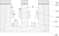
- the semiconductor structure includes a substrate; a channel inside the substrate, the channel being configured to form a buried gate structure; and a convex portion formed on an inner wall of the channel.
- the convex portion can increase a length of the channel, which meets a development direction of a small size, and meanwhile solve the short-channel effect, so as to solve the problem of reduction of the threshold voltage caused by the short-channel effect, and further improve the stability and electrical performance of a device.
- the substrate 100 may be, but is not limited to, a silicon substrate.
- the substrate 100 is made of any one or more mixtures of a silicon crystal, a germanium crystal, a silicon on insulator structure, a silicon on epitaxial layer structure, a compound semiconductor, and an alloy semiconductor.
- the compound semiconductor is any one or more mixtures of silicon carbide, gallium arsenide, gallium phosphide, indium phosphide, indium arsenide, and indium dysprosium.
- the alloy semiconductor is any one or more mixtures of SiGe, GaAsP, AlinAs, AlGaAs, GalnAs, GaInP, and GaInAsP. A description is provided in this specific implementation with an example in which the substrate 100 is a silicon substrate.
- the substrate 100 further includes an isolation region 101 .
- An oxide layer 102 and a SIN layer 103 are provided on a surface of the substrate 100 .
- a convex portion is arranged on an inner wall of the channel 105 .
- the inner wall of the channel 105 includes a bottom wall and a sidewall.
- FIG. 2 and FIG. 3 show an embodiment of a semiconductor structure with a convex portion arranged on a bottom wall. Referring to FIG. 2 and FIG. 3 , the convex portion may be arranged only on the bottom wall of the channel 105 .
- FIG. 4 and FIG. 5 show an embodiment of a semiconductor structure with a convex portion arranged on a sidewall. Referring to FIG. 4 and FIG. 5 , the convex portion may be arranged only on the sidewall of the channel 105 .
- FIG. 1 and FIG. 6 show an embodiment of a semiconductor structure with convex portions arranged on a sidewall and a bottom wall. Referring to FIG. 1 and FIG. 6 , the bottom wall and the sidewall of the channel 105 may be each provided with the convex portion.
- a number of the convex portion is not specifically limited.
- the bottom wall may be provided with one convex portion.
- the bottom wall may also be provided with a plurality of convex portions spaced.
- the sidewall may be provided with one convex portion.
- the sidewall may also be provided with a plurality of convex portions.
- the convex portion includes a first convex portion 170 arranged on the bottom wall of the channel 105 , and shallow trenches are formed between the first convex portion 170 and two sidewalls of the channel 105 respectively.
- the first convex portion 170 arranged on the bottom wall can increase a length of the channel by two heights H 2 of the first convex portion 170 .
- At least two first convex portions 170 are provided.
- One first convex portion 170 can increase the length of the channel by two heights H 2 of the first convex portion 170 .
- the length of the channel can be increased by two heights H 2 of the first convex portion 170 .
- the length of the channel can be increased more without increasing the depth of the channel.
- the at least two first convex portions 170 are spaced in a direction perpendicular to the two sidewalls of the channel.
- the at least two first convex portions 170 may be equally spaced.
- a distance between a sidewall and an adjacent first convex portion 170 may be equal to that between two adjacent first convex portions 170 .
- the at least two first convex portions 170 may be of a same size or different sizes.
- all first convex portions 170 may specifically have a uniform height H 2 and a uniform width W 3 .
- the first convex portions 170 may be formed simultaneously using a same process condition, which simplifies a manufacturing process and improves the manufacturing efficiency.
- the convex portion includes a second convex portion 190 arranged on a sidewall of the channel 105 .
- a distance W 2 (a width of the second convex portion 190 ) by which the second convex portion 190 protrudes from the sidewall of the channel increases the length of the channel 105 .
- the second convex portion 190 on one side can increase the length of the channel by two W 2 .
- At least one sidewall of the channel 105 is provided with the second convex portion 190 .
- At least two second convex portions 190 are provided on each sidewall. As illustrated in the figures, one second convex portion 190 can increase the length of the channel by two widths W 2 of the second convex portion 190 . Each time one second convex portion 190 is added, the length of the channel can be increased by two widths W 2 of the second convex portion 190 . When a plurality of second convex portions 190 are provided, the length of the channel can be increased more without increasing the depth of the channel.
- the at least two second convex portions 190 on each sidewall are spaced in a depth direction of the channel.
- the at least two second convex portions 190 may be equally spaced.
- the at least two second convex portions 190 may be of a same size or different sizes. For example, all second convex portions 190 may specifically have a uniform height H 1 and a uniform width W 2 .
- two sidewalls of the channel 105 are each provided with the second convex portion 190 .
- the two sidewalls of the channel 105 are each provided with the second convex portion 190 , so as to further increase the length of the channel.
- the second convex portions 190 on the two sidewalls of the channel 105 are arranged opposite to each other.
- the second convex portions 190 on the two sidewalls are arranged opposite to each other and can remain symmetric.
- the second convex portions 190 may be formed simultaneously using a same process condition without additional processes, which improves the manufacturing efficiency.
- a distance by which the first convex portion 170 protrudes from the bottom wall of the channel is referred to as a height H 2 of the first convex portion.
- the height H 2 of the first convex portion may specifically range from 10 nm to 30 nm.
- the height H 2 of the first convex portion 170 is above 10 nm, which can effectively increase the length of the channel.
- the height H 2 of the first convex portion 170 is controlled to be below 30 nm, which can prevent the influence on other properties of the semiconductor structure.
- a distance of the first convex portion 170 in the direction perpendicular to the two sidewalls may be referred to as a width W 3 of the first convex portion 170 .
- the width W 3 of the first convex portion 170 may specifically range from 5 nm to 10 nm.
- a distance by which the second convex portion 190 protrudes from the sidewall of the channel 105 is referred to as a width W 2 of the second convex portion 190 .
- the width W 2 of the second convex portion 190 may specifically range from 2 nm to 6 nm.
- a dimension of the second convex portion 190 in the depth direction of the channel 105 is referred to as a height H 1 of the second convex portion 190 .
- the height H 1 of the second convex portion 190 may specifically range from 20 nm to 60 nm.
- a distance H 3 from the second convex portion 190 to the surface of the substrate 100 may specifically range from 10 nm to 60 nm.
- the semiconductor structure further includes a gate structure.
- the gate structure may include a gate dielectric layer arranged on an inner wall surface of the channel and a gate electrode layer arranged on the gate dielectric layer. A surface of the gate dielectric layer may also be covered with an insulating layer.
- FIG. 26 is a flowchart of an embodiment of a semiconductor structure formation method according to the present application. Referring to FIG. 26 , the formation method includes the following steps.
- a channel is formed on the substrate.
- a convex portion is formed on an inner wall of the channel.
- the convex portion is formed on the inner wall of the channel configured to form a buried gate structure.
- the convex portion can increase a length of the channel, which meets a development direction of a small size, and solve the short-channel effect, so as to solve the problem of reduction of the threshold voltage caused by the short-channel effect, and further improve the stability and electrical performance of the device.
- FIG. 7 to FIG. 21 are schematic diagrams of cross-sectional structures at various stages during the formation of a semiconductor structure according to an embodiment of the present application.
- the semiconductor structure formation method according to the embodiment of the present application is further described below with reference to FIG. 1 to FIG. 21 .
- an isolation region 101 is formed on the substrate 100 provided in step S 100 shown in FIG. 7 , the surface of the substrate 100 is sequentially provided with an oxide layer 102 , a SIN layer 103 and a second sacrificial layer 104 , and the second sacrificial layer is provided with a photoresist layer 200 .
- a pattern 201 is defined on the silicon substrate 100 , the silicon substrate is etched by using the photoresist layer 200 , the second sacrificial layer 104 , the SIN layer 103 and the oxide layer 102 as an etch barrier layer, the excessive etch barrier layer is removed to form the channel 105 on the substrate, and a structure shown in FIG. 8 is obtained.
- the pattern 201 defined by the structure may be directly defined by lighting, or the pattern may be defined first by lighting and then by pitch double, which may be determined by a width W 1 of a buried gate during specific implementation.
- the width W 1 of the buried gate may specifically range from 5 nm to 80 nm.
- a thickness of the etch barrier layer may be between 20 nm and 250 nm.
- the etch barrier layer may be made of any material with a selectivity ratio meeting a requirement, which is not described in detail herein.
- step S 300 of forming a convex portion on an inner wall of the channel includes the following step.
- a first convex portion 170 is formed on a bottom wall of the channel, and shallow trenches are formed between the first convex portion 170 and two sidewalls of the channel respectively.
- S 310 of forming a first convex portion 170 on a bottom wall of the channel includes the following steps.
- a first sacrificial layer 106 is formed on the inner wall of the channel; the first sacrificial layer 106 covers a sidewall and the bottom wall of the channel 105 ; and a structure obtained is shown in FIG. 9 .
- the first sacrificial layer 106 at the bottom is removed to expose the bottom wall of the channel.
- the first sacrificial layer 106 may be etched back to remove the first sacrificial layer 106 at the bottom, the first sacrificial layer 106 on the sidewall is retained, and a structure obtained is shown in FIG. 10 .
- FIG. 10 in the specific implementation, when the first sacrificial layer 106 is etched back, the first sacrificial layer at the bottom is completely removed along the first sacrificial layer 106 on two sidewalls to expose the bottom wall of the channel 105 .
- a first extension layer 107 is formed on the exposed bottom wall.
- the first extension layer 107 may be formed between the first sacrificial layers 106 from the exposed bottom wall by epitaxial growth, and a structure obtained is shown in FIG. 11 .
- part of the first extension layer 107 is removed to enable the remaining first extension layer 107 to protrude from the bottom wall of the channel by a first height.
- the first extension layer 107 deposited between the first sacrificial layers 106 is etched back to remove an upper part of the first extension layer 107 .
- An etch-back depth is related to an etch time.
- a height of the remaining first extension layer 107 is a design height H 2 by controlling the etch time, and a structure obtained is shown in FIG. 12 .
- the first sacrificial layer 106 is removed; that is, the first convex portion 170 is formed on the bottom wall of the channel 105 .
- the first sacrificial layer 106 may be removed by wet removal or dry removal, and a structure obtained is shown in FIG. 13 .
- S 311 to S 312 other suitable manners may also be adopted to form the first sacrificial layer 106 on the sidewall of the channel 105 and expose the bottom wall of the channel 105 . Then, S 313 is implemented to form the first extension layer 107 on the bottom wall of the channel 105 exposed between the first sacrificial layers 106 formed on the sidewall.
- first convex portion 170 In the embodiment of the semiconductor structure shown in FIG. 13 , only one first convex portion 170 is formed on the bottom wall. In other embodiments, a plurality of first convex portions 170 may be formed on the bottom wall. A specific manner of forming a plurality of first convex portions 170 on the bottom wall may be illustrated through the following embodiment.
- FIG. 19 is a schematic structural diagram obtained according to another embodiment in which the first sacrificial layer 106 at the bottom is removed.
- the step of removing the first sacrificial layer 106 at the bottom to expose the bottom wall of the channel 105 includes:
- the first sacrificial layer 106 may be etched back to remove the first sacrificial layer 106 at the bottom at intervals to form the at least two notches exposing the bottom wall of the channel 105 .
- a structure obtained is shown in FIG. 19 .
- the semiconductor structure with at least two first convex portions 170 formed on the bottom wall of the channel 105 may be obtained by continuing other steps of forming the first convex portion 170 on the basis of the structures obtained in the above embodiments.
- the step of forming at least two first convex portions 170 on the bottom wall of the channel 105 includes the following steps.
- a first sacrificial layer 106 is formed on the inner wall of the channel; the first sacrificial layer 106 covers a sidewall and the bottom wall of the channel 105 ; and a structure obtained is shown in FIG. 9 .
- the first sacrificial layer 106 at the bottom is removed at intervals to enable the first sacrificial layer 106 to form, at intervals in a direction perpendicular to two sidewalls of the channel 105 , at least two notches exposing the bottom wall of the channel 105 .
- the first sacrificial layer 106 may be etched back to form the at least two notches exposing the bottom wall of the channel 105 . A structure obtained is shown in FIG. 19 .
- a first extension layer 107 is formed on the exposed bottom wall.
- the first extension layer 107 may be formed between the first sacrificial layers 106 from the exposed bottom wall by epitaxial growth.
- the first extension layer 107 fills the notch exposing the bottom wall.
- a height of the first extension layer 107 is generally greater than a design height of the first convex portion 170 . For example, a structure obtained is shown in FIG. 20 .
- part of the first extension layer 107 is removed to enable the remaining first extension layer 107 to protrude from the bottom wall of the channel 105 by a first height (i.e., the design height of the first convex portion 170 ).
- the first extension layer 107 is etched back to remove an upper part of the first extension layer 107 .
- An etch-back depth is related to an etch time.
- a height of the remaining first extension layer 107 is a design height H 2 by controlling the etch time, and a structure obtained is shown in FIG. 21 .
- the first sacrificial layer 106 is removed, so that the first convex portion 170 is formed on the bottom wall of the channel 105 .
- the first sacrificial layer 106 may be removed by wet removal or dry removal, and a structure obtained is shown in FIG. 3 .
- the step of forming at least two first convex portions 170 on the bottom wall may also involve etching back the first extension layer 107 by using an appropriate pattern so as to form a plurality of first convex portions 170 on the bottom wall in step S 314 of removing part of the first extension layer 107 .
- all or some steps of S 311 to S 315 may also be repeated to form one first convex portion 170 at a time, so as to form at least two first convex portions 170 on the bottom wall.
- the first convex portion 170 may be formed on the bottom wall of the channel 105 through the above process. Related processes of forming a gate structure may be performed subsequently. Alternatively, a process of forming a convex portion on the sidewall is further performed to form convex portions on the bottom wall and the sidewall of the channel 105 respectively.
- the step of forming a convex portion on an inner wall of the channel 105 includes: forming a second convex portion 190 on at least one sidewall of the channel 105 .
- the step of forming a second convex portion 190 on the sidewall of the channel 105 may be directly forming the second convex portion 190 after the channel is formed.
- the second convex portion 190 may be formed only on the sidewall of the channel 105 .
- the second convex portion 190 may also be formed on the sidewall after the first convex portion 170 is formed on the bottom wall.
- convex portions may be formed on the sidewall and the bottom wall of the channel 105 respectively.
- the second convex portion 190 is formed after the first convex portion 170 is formed. Specifically, after the step of forming a first convex portion 170 on a bottom wall of the channel 105 , the method further includes the following steps.
- a second sacrificial layer 108 of a second height is formed at a bottom of the channel 105 , the second height being greater than the first height.
- the second sacrificial layer 108 covers the first convex portion 170 formed on the bottom wall, so that the first convex portion 170 is not affected in subsequent steps.
- One or at least two first convex portions 170 may be formed on the bottom wall.
- S 316 of forming a second sacrificial layer 108 of a second height may include: S 3161 : depositing the second sacrificial layer 108 in the channel.
- S 3161 depositing the second sacrificial layer 108 in the channel.
- a structure obtained is shown in FIG. 14 .
- S 3162 part of the second sacrificial layer 108 is removed to enable a height of the remaining second sacrificial layer 108 to be a second height.
- the deposited second sacrificial layer 108 is etched back, an etch-back depth may be controlled through an etch time, so that the height of the remaining second sacrificial layer 108 is the second height, the second sacrificial layer 108 covers the first convex portion 170 , and a structure obtained is shown in FIG. 15 .
- the second height is a distance from the second convex portion 190 to the bottom wall of the channel.
- a second extension layer 109 is formed on the inner wall of the channel 105 on which the second sacrificial layer 108 is formed. Specifically, the second extension layer 109 is deposited on the sidewall of the channel 105 and a surface of the second sacrificial layer 108 at the bottom, and a structure obtained is shown in FIG. 16 .
- the second extension layer 109 at the bottom is removed to expose the second sacrificial layer 108 and part of the second extension layer 109 on the sidewall is removed, so as to enable a dimension of the second extension layer 109 remaining on the sidewall of the channel 105 along a depth direction of the channel to reach a design dimension (H 1 ).
- the deposited second extension layer 109 is etched back, an etch-back depth of the second extension layer 109 on the sidewall may be controlled through an etch time, and a structure obtained is shown in FIG. 17 .
- the second extension layer 109 is formed on the sidewall of the channel 105 by epitaxial growth. Then, part of the second extension layer 109 on the sidewall is removed, so as to enable a dimension of the second extension layer 109 remaining on the sidewall of the channel 105 along a depth direction of the channel to reach a design dimension (H 1 ).
- the second sacrificial layer 108 is removed, so that the second convex portion 190 can be formed on the sidewall of the channel 105 .
- the second sacrificial layer 108 may be removed by dry removal, and a structure obtained is shown in FIG. 18 .
- one second convex portion 190 is formed on the sidewall of the channel 105 .
- At least two second convex portions 190 may be formed on the sidewall of the channel 105 by repeating some steps including S 317 and S 318 .
- the step of forming at least two second convex portions 190 on the sidewall of the channel 105 includes the following step.
- a second sacrificial layer 108 of a second height is formed at a bottom of the channel 105 , the second height being greater than the first height.
- the second sacrificial layer 108 covers the first convex portion 170 formed on the bottom wall, so that the first convex portion 170 is not affected in subsequent steps.
- One or at least two first convex portions 170 may be formed on the bottom wall.
- the step of forming a second sacrificial layer 108 of a second height may include: depositing the second sacrificial layer 108 in the channel.
- the second sacrificial layer 108 is formed on the basis of the structure obtained in S 315 , a structure obtained is shown in FIG. 14 . Part of the second sacrificial layer 108 is removed to enable a height of the remaining second sacrificial layer 108 to be a second height.
- the deposited second sacrificial layer 108 is etched back, an etch-back depth may be controlled through an etch time, so that the height of the remaining second sacrificial layer 108 is the second height, the second sacrificial layer 108 covers the first convex portion 170 , and a structure obtained is shown in FIG. 15 .
- the second height is a distance from the second convex portion 190 to the bottom wall of the channel.
- the second extension layer 109 is formed on the inner wall of the channel 105 on which the second sacrificial layer 108 is formed. Specifically, referring to S 317 , the second extension layer 109 is deposited on the sidewall of the channel 105 and the surface of the second sacrificial layer 108 at the bottom, and the structure obtained is shown in FIG. 16 .
- the second extension layer 109 at the bottom is removed to expose the second sacrificial layer 108 and part of the second extension layer 109 on the sidewall is removed, so as to enable a dimension of the second extension layer 109 remaining on the sidewall of the channel 105 along a depth direction of the channel to reach a design dimension (H 1 ).
- the deposited second extension layer 109 is etched back, the etch-back depth of the second extension layer 109 on the sidewall may be controlled through the etch time, and the structure obtained is shown in FIG. 17 .
- a third sacrificial layer 108 a is formed on the second sacrificial layer 108 in the channel 105 to enable the third sacrificial layer 108 a filling the channel 105 to cover the remaining second extension layer 109 .
- a specific method for forming the third sacrificial layer 108 a may be obtained with reference to S 316 , and is not described in detail herein. A structure obtained is shown in FIG. 22 .
- a third extension layer 109 a is formed on the inner wall of the channel 105 .
- a specific method for forming the third extension layer 109 a may be obtained with reference to S 317 , and is not described in detail herein.
- a structure obtained is shown in FIG. 23 .
- the third extension layer 109 a at the bottom is removed to expose the third sacrificial layer 108 a and part of the third extension layer 109 a on the sidewall is removed, so as to enable a dimension of the third extension layer remaining on the sidewall of the channel along a depth direction of the channel to reach a design dimension.
- a specific method for removing part of the third extension layer 109 a at the bottom and on the sidewall in S 336 may be obtained with reference to S 318 , and is not described in detail herein. A structure obtained is shown in FIG. 24 .
- a plurality of second convex portions 190 may be formed on the sidewall of the channel 105 by repeating the step of forming a single second convex portion 190 .
- the second convex portion 190 is formed after the channel 105 is formed, and a semiconductor structure with the second convex portion 190 formed only on the sidewall of the channel 105 can be obtained.
- the manner of forming the second convex portion 190 may be obtained with reference to S 316 to S 319 in the previous embodiment.
- the step of forming a second convex portion 190 on at least one sidewall of the channel 105 includes the following steps.
- a second sacrificial layer 108 of a third height is formed at a bottom of the channel 105 .
- the second sacrificial layer 108 may be deposited in the channel 105 at first.
- the deposited second sacrificial layer 108 is etched back, and an etch-back depth may be controlled through an etch time, so that the height of the remaining second sacrificial layer 108 is the second height.
- the second height is a distance from the second convex portion 190 to the bottom wall of the channel.
- a second extension layer is formed on the inner wall of the channel 105 on which the second sacrificial layer 108 is formed. Specifically, referring to S 317 , the second extension layer 109 is deposited on the sidewall of the channel 105 and the surface of the second sacrificial layer 108 at the bottom.
- the second extension layer 109 at the bottom is removed to expose the second sacrificial layer 108 and part of the second extension layer 109 on the sidewall is removed, so as to enable a dimension of the second extension layer 109 remaining on the sidewall of the channel 105 along a depth direction of the channel to reach a design dimension (H 1 ).
- the deposited second extension layer 109 is etched back, and the etch-back depth of the second extension layer 109 on the sidewall may be controlled through the etch time.
- the second sacrificial layer is removed, so that the second convex portion 190 can be formed on the sidewall of the channel 105 .
- the second sacrificial layer 108 may be removed by dry removal.
- a specific method for forming at least two second convex portions 190 only on the sidewall of the channel 105 may be obtained with reference to steps S 331 to S 337 in the above embodiment.
- the step of forming at least two second convex portions 190 on the sidewall of the channel 105 includes the following step.
- a second sacrificial layer of a third height is formed at a bottom of the channel. Details may be obtained with reference to S 331 and are not described herein.
- a second extension layer is formed on the inner wall of the channel on which the second sacrificial layer is formed. Details may be obtained with reference to S 332 and are not described herein.
- the second extension layer at the bottom is removed to expose the second sacrificial layer and part of the second extension layer on the sidewall is removed, so as to enable a dimension of the second extension layer remaining on the sidewall of the channel along a depth direction of the channel to reach a design dimension. Details may be obtained with reference to S 333 and are not described herein.
- a third sacrificial layer is formed in the channel to enable the third sacrificial layer filling the channel to cover the remaining second extension layer. Details may be obtained with reference to S 334 and are not described herein.
- a third extension layer is formed on the inner wall of the channel. Details may be obtained with reference to S 335 and are not described herein.
- the third extension layer at the bottom is removed to expose the third sacrificial layer and part of the third extension layer on the sidewall is removed, so as to enable a dimension of the third extension layer remaining on the sidewall of the channel along a depth direction of the channel to reach a design dimension. Details may be obtained with reference to S 336 and are not described herein.
- the third sacrificial layer and the second sacrificial layer are removed. Details may be obtained with reference to S 337 and are not described herein.
- materials of the sacrificial layers are not limited, which may be an oxide layer, a nitride layer, a carbon layer, etc.
- Materials and formation manners of the extension layers are not limited.
- the extension layer may be formed by epitaxial growth or deposition. Specifically, molecular beam epitaxial growth or atomic layer deposition may be adopted.
- an embodiment of the present application provides a memory, including the semiconductor structure described in any one of the above embodiments.
Landscapes
- Engineering & Computer Science (AREA)
- Manufacturing & Machinery (AREA)
- Non-Volatile Memory (AREA)
- Semiconductor Memories (AREA)
Abstract
Description
-
- a substrate;
- a channel located in the substrate, the channel being configured to form a gate structure; and
- a convex portion arranged on an inner wall of the channel.
-
- providing a substrate;
- forming a channel on the substrate; and
- forming a convex portion on an inner wall of the channel.
-
- a
substrate 100; - a
channel 105 located in thesubstrate 100, thechannel 105 being configured to form a gate structure; and - a convex portion arranged on an inner wall of the
channel 105.
- a
Claims (16)
Applications Claiming Priority (3)
| Application Number | Priority Date | Filing Date | Title |
|---|---|---|---|
| CN202110750964.8A CN113471201B (en) | 2021-07-02 | 2021-07-02 | Semiconductor structure and method of forming same, memory |
| CN202110750964.8 | 2021-07-02 | ||
| PCT/CN2021/106500 WO2023272787A1 (en) | 2021-07-02 | 2021-07-15 | Semiconductor structure, method for forming same, and memory |
Related Parent Applications (1)
| Application Number | Title | Priority Date | Filing Date |
|---|---|---|---|
| PCT/CN2021/106500 Continuation WO2023272787A1 (en) | 2021-07-02 | 2021-07-15 | Semiconductor structure, method for forming same, and memory |
Publications (2)
| Publication Number | Publication Date |
|---|---|
| US20230005929A1 US20230005929A1 (en) | 2023-01-05 |
| US12171094B2 true US12171094B2 (en) | 2024-12-17 |
Family
ID=77877565
Family Applications (1)
| Application Number | Title | Priority Date | Filing Date |
|---|---|---|---|
| US17/486,696 Active 2043-01-06 US12171094B2 (en) | 2021-07-02 | 2021-09-27 | Semiconductor structure, formation method thereof and memory |
Country Status (3)
| Country | Link |
|---|---|
| US (1) | US12171094B2 (en) |
| CN (1) | CN113471201B (en) |
| WO (1) | WO2023272787A1 (en) |
Citations (10)
| Publication number | Priority date | Publication date | Assignee | Title |
|---|---|---|---|---|
| KR20060026262A (en) | 2004-09-20 | 2006-03-23 | 삼성전자주식회사 | Gate Forming Method of Recessed Cell Array Transistor and Its Gate Structure |
| KR20060042460A (en) | 2004-11-09 | 2006-05-15 | 삼성전자주식회사 | Transistor manufacturing method having recess channel of semiconductor device |
| KR100724572B1 (en) | 2006-02-14 | 2007-06-04 | 삼성전자주식회사 | Method for manufacturing a transistor having a recessed gate electrode |
| CN101009279A (en) | 2006-01-23 | 2007-08-01 | 海力士半导体有限公司 | Semiconductor device and method for manufacturing the same |
| KR20080010664A (en) | 2006-07-27 | 2008-01-31 | 주식회사 하이닉스반도체 | Method of forming a semiconductor device |
| US20080087948A1 (en) | 2006-10-16 | 2008-04-17 | Hynix Semiconductor Inc. | Semiconductor device and method for manufacturing the same |
| US20080128800A1 (en) | 2006-12-04 | 2008-06-05 | Samsung Electronics Co., Ltd. | Field effect transistors including recessed forked gate structures and methods of fabricating the same |
| CN102738222A (en) | 2011-04-07 | 2012-10-17 | 南亚科技股份有限公司 | Recessed gate transistor with cylindrical fins |
| CN108717947A (en) | 2017-08-10 | 2018-10-30 | 长鑫存储技术有限公司 | Transistor structure and manufacturing method of a semiconductor memory |
| US20200203427A1 (en) * | 2018-12-21 | 2020-06-25 | SK Hynix Inc. | Nonvolatile memory device having stacked cell transistors and operating method thereof |
-
2021
- 2021-07-02 CN CN202110750964.8A patent/CN113471201B/en active Active
- 2021-07-15 WO PCT/CN2021/106500 patent/WO2023272787A1/en not_active Ceased
- 2021-09-27 US US17/486,696 patent/US12171094B2/en active Active
Patent Citations (12)
| Publication number | Priority date | Publication date | Assignee | Title |
|---|---|---|---|---|
| KR20060026262A (en) | 2004-09-20 | 2006-03-23 | 삼성전자주식회사 | Gate Forming Method of Recessed Cell Array Transistor and Its Gate Structure |
| KR20060042460A (en) | 2004-11-09 | 2006-05-15 | 삼성전자주식회사 | Transistor manufacturing method having recess channel of semiconductor device |
| CN101009279A (en) | 2006-01-23 | 2007-08-01 | 海力士半导体有限公司 | Semiconductor device and method for manufacturing the same |
| KR100724572B1 (en) | 2006-02-14 | 2007-06-04 | 삼성전자주식회사 | Method for manufacturing a transistor having a recessed gate electrode |
| KR20080010664A (en) | 2006-07-27 | 2008-01-31 | 주식회사 하이닉스반도체 | Method of forming a semiconductor device |
| KR100909763B1 (en) | 2006-07-27 | 2009-07-29 | 주식회사 하이닉스반도체 | Method of forming a semiconductor device |
| US20080087948A1 (en) | 2006-10-16 | 2008-04-17 | Hynix Semiconductor Inc. | Semiconductor device and method for manufacturing the same |
| US20080128800A1 (en) | 2006-12-04 | 2008-06-05 | Samsung Electronics Co., Ltd. | Field effect transistors including recessed forked gate structures and methods of fabricating the same |
| CN102738222A (en) | 2011-04-07 | 2012-10-17 | 南亚科技股份有限公司 | Recessed gate transistor with cylindrical fins |
| CN102738222B (en) | 2011-04-07 | 2015-02-25 | 南亚科技股份有限公司 | Recessed gate transistor with cylindrical fins |
| CN108717947A (en) | 2017-08-10 | 2018-10-30 | 长鑫存储技术有限公司 | Transistor structure and manufacturing method of a semiconductor memory |
| US20200203427A1 (en) * | 2018-12-21 | 2020-06-25 | SK Hynix Inc. | Nonvolatile memory device having stacked cell transistors and operating method thereof |
Non-Patent Citations (2)
| Title |
|---|
| International Search Report cited in PCT/CN2021/106500, mailed Mar. 28, 2022, 9 pages. |
| Second Office Action of the Chinese application No. 202110750964.8, issued on Nov. 9, 2023. 19 pages with English translation. |
Also Published As
| Publication number | Publication date |
|---|---|
| WO2023272787A1 (en) | 2023-01-05 |
| CN113471201B (en) | 2024-03-29 |
| US20230005929A1 (en) | 2023-01-05 |
| CN113471201A (en) | 2021-10-01 |
Similar Documents
| Publication | Publication Date | Title |
|---|---|---|
| CN111223779B (en) | Semiconductor structure and forming method thereof | |
| US9219114B2 (en) | Partial FIN on oxide for improved electrical isolation of raised active regions | |
| US8507349B2 (en) | Semiconductor device employing fin-type gate and method for manufacturing the same | |
| US6291310B1 (en) | Method of increasing trench density for semiconductor | |
| KR100920045B1 (en) | Semiconductor device and manufacturing method thereof | |
| CN113707608B (en) | Semiconductor structure and preparation method thereof | |
| CN112466890B (en) | A 3D NAND memory device and its manufacturing method | |
| US12171094B2 (en) | Semiconductor structure, formation method thereof and memory | |
| KR101129867B1 (en) | Method for manufacturig the semiconductor device | |
| US9496343B2 (en) | Secondary use of aspect ratio trapping holes as eDRAM structure | |
| US12225717B2 (en) | Semiconductor device with dielectric structure having enlargemant portion surrounding word line | |
| US7585727B2 (en) | Method for fabricating semiconductor device having bulb-shaped recess gate | |
| CN109346408B (en) | MOS transistor and forming method thereof, and forming method of flash memory | |
| US20250140557A1 (en) | Method for forming a reduced size feature | |
| CN113964036B (en) | Manufacturing method of semiconductor structure and electronic equipment | |
| US11869801B2 (en) | Semiconductor manufacturing method | |
| US20240128357A1 (en) | 3d-transistor structure with precise geometries | |
| KR100636669B1 (en) | Manufacturing Method of DRAM Memory Cell | |
| KR100929630B1 (en) | Semiconductor element and manufacturing method thereof | |
| KR100960926B1 (en) | Manufacturing method of MOSFET device | |
| CN120018537A (en) | Semiconductor structure and method for manufacturing the same | |
| CN117835695A (en) | Method for preparing semiconductor structure and semiconductor structure | |
| CN117766393A (en) | Semiconductor structures and methods of forming them | |
| CN117476750A (en) | Semiconductor structure and manufacturing method thereof | |
| CN118841432A (en) | Semiconductor structure and forming method thereof |
Legal Events
| Date | Code | Title | Description |
|---|---|---|---|
| FEPP | Fee payment procedure |
Free format text: ENTITY STATUS SET TO UNDISCOUNTED (ORIGINAL EVENT CODE: BIG.); ENTITY STATUS OF PATENT OWNER: LARGE ENTITY |
|
| STPP | Information on status: patent application and granting procedure in general |
Free format text: DOCKETED NEW CASE - READY FOR EXAMINATION |
|
| AS | Assignment |
Owner name: CHANGXIN MEMORY TECHNOLOGIES, INC., CHINA Free format text: ASSIGNMENT OF ASSIGNORS INTEREST;ASSIGNOR:WAN, WEI;REEL/FRAME:058071/0656 Effective date: 20210816 |
|
| STPP | Information on status: patent application and granting procedure in general |
Free format text: NON FINAL ACTION MAILED |
|
| STPP | Information on status: patent application and granting procedure in general |
Free format text: RESPONSE TO NON-FINAL OFFICE ACTION ENTERED AND FORWARDED TO EXAMINER |
|
| STPP | Information on status: patent application and granting procedure in general |
Free format text: EX PARTE QUAYLE ACTION MAILED |
|
| STPP | Information on status: patent application and granting procedure in general |
Free format text: RESPONSE TO EX PARTE QUAYLE ACTION ENTERED AND FORWARDED TO EXAMINER |
|
| STPP | Information on status: patent application and granting procedure in general |
Free format text: NOTICE OF ALLOWANCE MAILED -- APPLICATION RECEIVED IN OFFICE OF PUBLICATIONS |
|
| STPP | Information on status: patent application and granting procedure in general |
Free format text: PUBLICATIONS -- ISSUE FEE PAYMENT VERIFIED |
|
| STCF | Information on status: patent grant |
Free format text: PATENTED CASE |