US12165610B2 - Method of operating display driver integrated circuit, power management integrated circuit and electronic device including the same, and method of operating the same - Google Patents
Method of operating display driver integrated circuit, power management integrated circuit and electronic device including the same, and method of operating the same Download PDFInfo
- Publication number
- US12165610B2 US12165610B2 US18/097,948 US202318097948A US12165610B2 US 12165610 B2 US12165610 B2 US 12165610B2 US 202318097948 A US202318097948 A US 202318097948A US 12165610 B2 US12165610 B2 US 12165610B2
- Authority
- US
- United States
- Prior art keywords
- level
- voltage
- pmic
- ddi
- logic
- Prior art date
- Legal status (The legal status is an assumption and is not a legal conclusion. Google has not performed a legal analysis and makes no representation as to the accuracy of the status listed.)
- Active
Links
Images





Classifications
-
- G—PHYSICS
- G09—EDUCATION; CRYPTOGRAPHY; DISPLAY; ADVERTISING; SEALS
- G09G—ARRANGEMENTS OR CIRCUITS FOR CONTROL OF INDICATING DEVICES USING STATIC MEANS TO PRESENT VARIABLE INFORMATION
- G09G5/00—Control arrangements or circuits for visual indicators common to cathode-ray tube indicators and other visual indicators
- G09G5/003—Details of a display terminal, the details relating to the control arrangement of the display terminal and to the interfaces thereto
-
- G—PHYSICS
- G09—EDUCATION; CRYPTOGRAPHY; DISPLAY; ADVERTISING; SEALS
- G09G—ARRANGEMENTS OR CIRCUITS FOR CONTROL OF INDICATING DEVICES USING STATIC MEANS TO PRESENT VARIABLE INFORMATION
- G09G2310/00—Command of the display device
- G09G2310/02—Addressing, scanning or driving the display screen or processing steps related thereto
- G09G2310/0243—Details of the generation of driving signals
-
- G—PHYSICS
- G09—EDUCATION; CRYPTOGRAPHY; DISPLAY; ADVERTISING; SEALS
- G09G—ARRANGEMENTS OR CIRCUITS FOR CONTROL OF INDICATING DEVICES USING STATIC MEANS TO PRESENT VARIABLE INFORMATION
- G09G2330/00—Aspects of power supply; Aspects of display protection and defect management
- G09G2330/02—Details of power systems and of start or stop of display operation
-
- G—PHYSICS
- G09—EDUCATION; CRYPTOGRAPHY; DISPLAY; ADVERTISING; SEALS
- G09G—ARRANGEMENTS OR CIRCUITS FOR CONTROL OF INDICATING DEVICES USING STATIC MEANS TO PRESENT VARIABLE INFORMATION
- G09G2330/00—Aspects of power supply; Aspects of display protection and defect management
- G09G2330/02—Details of power systems and of start or stop of display operation
- G09G2330/028—Generation of voltages supplied to electrode drivers in a matrix display other than LCD
Definitions
- Example embodiments of the disclosure relate to a method of operating a display driver integrated circuit (DDI), a power management integrated circuit (PMIC), and an electronic device including the same.
- DCI display driver integrated circuit
- PMIC power management integrated circuit
- a display device may include a display panel displaying an image, and a display driver integrated circuit driving the display panel, and a PMIC.
- the DDI may drive the display panel by receiving image data from an external host and applying an image signal corresponding to the received image data to a source line of the display panel.
- the DDI and the PMIC vary, via S-wire communication, the analog power and the panel driving power of the DDI according to a panel driving mode.
- DDI display driver integrated circuit
- PMIC power management integrated circuit
- an operating method of a DDI may include determining whether a change to a level of a first logic voltage supplied to a logic circuit of the DDI is required, based on determining that a change to the level of the first logic voltage is required, transmitting a logic voltage setting command to a PMIC, and receiving, from the PMIC, a second logic voltage having a level different from the first logic voltage and corresponding to the logic voltage setting command.
- a PMIC may include a first voltage generator configured to generate a first voltage supplied to a panel, and determine a level of the first voltage in response to a first control signal, a second voltage generator configured to generate a second voltage supplied to an analog circuit of a DDI, and determine a level of the second voltage in response to a second control signal, a third voltage generator configured to generate a third voltage supplied to the DDI, and determine a level of the third voltage in response to a third control signal, and a logic circuit configured to receive at least one power setting command via communication with the DDI, and generate the first control signal, the second control signal, and the third control signal.
- an electronic device may include an application processor, a DDI driven by an analog voltage and a logic voltage and configured to receive a power control command from the application processor, and generate at least one power setting command, a panel configured to receive a panel voltage, and a PMIC configured to communicate with the DDI, and generate, in response to the at least one power setting command, the panel voltage, the analog voltage, and the logic voltage.
- a level of the logic voltage may be lowered from a first level to a second level lower than the first level during low-frequency driving.
- an operating method of a DDI may include receiving, from an application processor, a power control command corresponding to voltage control, setting, in response to the power control command, a logic voltage control mode with respect to a PMIC setting register, determining whether an operation mode is a low-frequency operation mode, based on the operation mode being determined to be the low-frequency operation mode, transmitting, to a PMIC, a power setting command for lowering a logic voltage, and receiving, from the PMIC, a logic voltage corresponding to the power setting command.
- a DDI may include a power management control register configured to receive a power control command from an application processor, and store power management control information corresponding to the power control command, an interface circuit configured to communicate with a PMIC based on the power management control information, and transmit, to the PMIC, a power setting command for changing a level of a logic voltage, and a regulator configured to receive the logic voltage from the PMIC.
- the level of the logic voltage may be determined based on the power setting command.
- FIG. 1 is a diagram illustrating a general display device according to an example embodiment
- FIG. 2 is a diagram illustrating an example in which power reduction is implemented by changing a panel voltage depending on a screen content according to an example embodiment
- FIG. 3 is a diagram illustrating a display device according to an example embodiment
- FIGS. 4 A, 4 B, 4 C, 4 D and 4 E are diagrams illustrating a logic voltage being dynamically changed during low-frequency driving in a display device according to an example embodiment
- FIG. 5 is a diagram illustrating a logic voltage being dynamically changed during low-frequency driving in a display device according to an example embodiment
- FIG. 6 is a diagram illustrating a reduction in additional power consumption of a display device according to an example embodiment
- FIG. 7 is a flowchart illustrating a method of operating a display driver integrated circuit (DDI) according to an example embodiment
- FIG. 8 is a flowchart illustrating a method of operating a power management integrated circuit (PMIC) according to an example embodiment
- FIG. 9 is a diagram illustrating a power management method performed by a display system according to an example embodiment
- FIG. 10 is a diagram illustrating an electronic device according to an example embodiment.
- FIG. 11 is a diagram illustrating an electronic device according to an example embodiment.
- FIG. 1 is a diagram illustrating a general display device 100 according to an example embodiment.
- a display device 100 may include a panel 110 , a display driver integrated circuit (DDI) 120 , and a power management integrated circuit (PMIC) 130 .
- DCI display driver integrated circuit
- PMIC power management integrated circuit
- the panel 110 may be implemented to display image data.
- the panel 110 may be implemented as a thin film transistor-liquid crystal display (TFT-LCD) panel, a light emitting diode (LED) display panel, an organic LED (OLED) panel, an active matrix OLED (AMOLED) display panel, a flexible display panel, or the like.
- TFT-LCD thin film transistor-liquid crystal display
- LED light emitting diode
- OLED organic LED
- AMOLED active matrix OLED
- the panel 110 may include a plurality of pixels arranged in a matrix form having a plurality of rows and a plurality of columns. Each of the plurality of pixels may be connected to a plurality of data lines and a plurality of source lines.
- a pixel may include an RGB sub-pixel (e.g., a RGB stripe layout structure) or RGB sub-pixels (e.g., a pentile layout structure), as a structure in which sub-pixels such as red, green, and blue are arranged adjacent to each other.
- the pixel may be replaced with an RGB white (RGBW) sub-pixel arrangement structure.
- the DDI 120 may be implemented to control an operation of the panel 110 .
- the DDI 120 may change data transmitted from a processor to have a form for transmission to the panel 110 , and may transmit the changed data to the panel 100 .
- the DDI 120 may control a state (a sleep state, a display-on state, a display-off state, or the like) of the panel 110 .
- the PMIC 130 may be implemented to manage voltages, such as the panel voltage ELVSS and the analog voltage VLIN 1 , necessary for the panel 110 and the DDI 120 .
- the PMIC 130 may include a first voltage generator 131 , a second voltage generator 132 , and a logic circuit 134 .
- the first voltage generator 131 may generate a panel voltage ELVSS (e.g., a “first voltage”).
- the second voltage generator 132 may generate an analog voltage VLIN 1 (e.g., a “second voltage”) necessary for driving the DDI 120 .
- the logic circuit 134 may receive, from the DDI 120 , power setting commands AVDD_CMD and ELON_CMD necessary for power management.
- the first voltage generator 131 may vary a level of the panel voltage ELVSS in response to the first power setting command AVDD_CMD.
- the second voltage generator 132 may vary a level of the analog voltage VLN 1 in response to the second power setting command ELON_CMD.
- FIG. 2 is a diagram illustrating an example in which power reduction is implemented by changing a panel voltage ELVSS depending on a screen content according to an embodiment.
- the panel voltage ELVSS in a low power mode may be set to be lower than that in a normal mode.
- screen 200 shows a display device operating in a normal mode
- screen 202 shows the display device operating in a low power mode
- screen 204 shows the display device operating in a normal mode (e.g., the low power mode may be a low brightness mode and a normal mode may be a normal brightness or high brightness mode).
- Graph 206 shows the panel voltage ELVSS variation that occurs when switching between the modes.
- the analog voltage VLIN 1 and the panel voltage ELVSS may require ON/OFF or level control depending on a driving condition of the panel 110 .
- the DDI 120 may have voltage control for the analog voltage VLIN 1 and the panel voltage ELVSS.
- the logic voltage VDDR of the DDI may require power even when the panel is in an OFF state.
- the voltage control of the logic voltage VDDR may be possessed by a connected application processor (AP).
- a logic consumption current of the DDI may be low in a low-frequency driving section of a low temperature poly-silicon (LTPO) panel, and thus dynamic voltage scaling (DVS) for a voltage source may be possible.
- LTPO low temperature poly-silicon
- DVS dynamic voltage scaling
- PMIC implementation may not be possible.
- a display device may reduce a logic consumption current of a DDI via PMIC communication with the DDI in the LTPO panel.
- FIG. 3 is a diagram illustrating a display device 200 according to an example embodiment.
- the display device 200 may include a panel 210 , a DDI 220 , and a PMIC 230 .
- the DDI 220 may include a PMIC control register 221 , an interface circuit (IF) 222 , and a regulator 223 .
- the PMIC control register 222 may receive, from an AP, a power setting command related to voltage control of the PMIC 230 , and may store power control management information corresponding to the power setting command.
- the IF 222 may be implemented to communicate with the PMIC 230 via a communication interface.
- the communication interface may be an inter-integrated circuit (I2C) or S-wire communication interface. It should be understood that the communication interface is not limited thereto.
- the IF 222 may transmit, in response to a tearing effect (TE) signal, a power setting command to the PMIC 230 .
- the IF 222 may determine the number of communications with the PMIC 230 using touch sensitive panel (TSP) information.
- TSP touch sensitive panel
- the regulator 223 may be implemented to receive, from the PMIC 230 , the analog voltage VLIN 1 or the logic voltage VDDR, and to output a target voltage level.
- the regulator 223 may include a low drop-out (LDO) regulator.
- the DDI 220 may control the PMIC 230 using the power setting command.
- the PMIC 230 may be controlled depending on the number of toggling.
- the communication interface is the I2C interface
- the PMIC 230 may be controlled depending on an address.
- the DDI 220 may not be equipped with a micro control unit (MCU), and thus it may be difficult to secure software (S/W) flexibility.
- MCU micro control unit
- S/W software
- a register address map related to the logic voltage VDDR control and a voltage control sequence may be standardized.
- one DDI 220 controls one PMIC 230
- example embodiments are not limited thereto.
- a DDI according to example embodiments may control a plurality of PMICs.
- the PMIC 230 may add a path for controlling the logic voltage VDDR from the DDI 220 .
- simultaneous access to the PMIC 230 from the AP and the DDI 220 may be prevented by setting the AP and a protocol.
- the AP may change control of the logic voltage VDDR for the PMIC 230 by transmitting a special command to the DDI 220 .
- the control of the logic voltage VDDR in a normal mode may be possessed by the AP.
- the control of the logic voltage VDDR in a low-frequency operation mode may be possessed by the DDI 220 .
- the PMIC 230 may include a first voltage generator 231 , a second voltage generator 232 , a third voltage generator 233 , and a logic circuit 234 .
- the first voltage generator 231 may be implemented to generate the panel voltage ELVSS (e.g., a “first voltage”) according to a first control signal of the logic circuit 234 .
- the second voltage generator 232 may be implemented to generate the analog voltage VLIN 1 (e.g., a “second voltage”) according to a second control signal of the logic circuit 234 .
- the third voltage generator 233 may be implemented to generate the logic voltage VDDR (e.g., a “third voltage”) according to a third control signal of the logic circuit 234 .
- the logic circuit 234 may be implemented to receive, from the DDI 220 , commands AVDD_CMD and ELON_CMD, and to output the first control signal, the second control signal, and the third control signal.
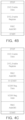
- FIGS. 4 A, 4 B, 4 C, 4 D and 4 E are diagrams illustrating VDDR being dynamically changed during low-frequency driving in a display device according to an example embodiment.
- the DDI 220 controls a state entering a sleep mode (SLPIN) and a state outside of a sleep mode (SLPOUT).
- SLPIN sleep mode
- SLPOUT state outside of a sleep mode
- an AP may assign, by a mobile industry processor interface (MIPI), command, voltage control for enabling a DVS function (DVS EN) to the DDI 220 .
- MIPI mobile industry processor interface
- the AP may recover, by the MIPI command, voltage control for disabling a DVS function (DVS DIV) from the DDI 220 .
- FIG. 4 B is a diagram illustrating a DVS enabling command received from an AP
- FIG. 4 C is a diagram illustrating a DVS disabling command received from the AP.
- the DVS enabling command may include a start bit, a PMIC address, a DVS enabling register address, DVS enabling data, and an end bit.
- the DVS disabling command may include a start bit, a PMIC address, a VDDR register address, VDDR register data, an R-start bit, a DVS enabling register address, DVS disabling data, and an end bit.
- a state outside of the sleep mode (SLPOUT), that is, a DVS enabling region may be secured.
- SLPOUT sleep mode
- an active display section may exist after a base synchronization (base sync) section.
- the DDI 220 may perform a DVS operation in response to a TE signal until a new image is updated on the panel 210 .
- the TE signal may be a signal for informing the AP that an update is available. Since it is before the update is performed, a VBIAS section corresponding to a blank frame may be repeated.
- PMIC power PMIC VDD
- LDO power LDO VDD
- PMIC VDD PMIC VDD
- LDO VDD LDO power
- a first power setting command may be transmitted to the PMIC 230 before the TE signal rises to a high level.
- the first power setting command may be a command for commanding a rise in a voltage level of VDDR/VLIN 1 .
- a second power setting command may be transmitted to the PMIC 230 .
- the second power setting command may be a command for commanding a fall in the voltage level of the VDDR/VLIN 1 .
- FIG. 4 D is a diagram illustrating a first power setting command
- FIG. 4 E is a diagram illustrating a second power setting command
- the first power setting command may include a start bit, a PMIC address, a VDDR register address, VDDR register data, and an end bit.
- the VDDR register data may include information for raising a voltage level of VDDR.
- the second power setting command may include a start bit, a PMIC address, a VDDR register address, VDDR register data, and an end bit.
- the VDDR register data may include information for lowering the voltage level of the VDDR.
- a time point of transmitting the first and second power setting commands may be determined in consideration of internal power stabilization time and I2C command time.
- the DDI 220 may dynamically change the logic voltage VDDR by communicating with the PMIC 230 during low-frequency driving. For example, during low-frequency driving, the logic voltage VDDR may be changed from about 1.8V to about 1.3V. Accordingly, the DDI 220 may reduce logic power.
- a power setting command CMD may be transmitted via the I2C interface.
- the power setting command CMD may be transmitted via an S-wire interface.
- the CMDs may include VDDR/VLIN 1 down commands 450 and VDDR VLIN 1 up commands 452 .
- the DDI 220 may not verify a point in time at which an application of the AP needs to update an image, such as a touch event.
- a TE may be a signal for periodically informing the AP of a point in time at which a video update is available.
- the logic voltage VDDR may need to be changed from about 1.3V to about 1.8V in advance by communicating with the PMIC 230 before TE enabling. When there is no image update, the logic voltage VDDR may need to be changed back from about 1.8V to about 1.3 V after TE disabling.
- the DDI 220 may need to determine a time point of communicating with the PMIC 230 in consideration of power stabilization time of the PMIC 230 and a timing of communication with the PMIC 230 .
- the DDI 220 may determine a communication time point using a control register.
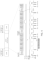
- FIG. 5 is a diagram illustrating a display device dynamically changing a logic voltage VDDR during low-frequency driving according to an example embodiment.
- a power setting command CMD may be transmitted via the I2C interface.
- the power setting command CMD may be transmitted via an S-wire interface.
- the CMDs may include VDDR/VLIN 1 down commands 550 and VDDR VLIN 1 up commands 552 .
- a DDI 220 may reduce the number of communications with the PMIC 230 using TSP information TSP_INFO related to a touch event and a communication channel, thereby reducing additional logic power.
- the DDI 220 may adjust a TE enabling cycle via a protocol with an AP.
- the DDI 220 may not need to communicate with the PMIC 230 in a section in which there is no TE enabling.
- the DDI 220 may additionally secure holding time in a low power supply voltage (1.3V) state.
- a TE signal may be enabled from when a touch event interrupt signal TSP_IRQ is received until a touch event reset signal TSP_RST is received.
- FIG. 6 is a diagram illustrating a reduction in additional power consumption in a display device according to an example embodiment.
- a point in time at which memory data of the DDI 220 is charged to the capacitor of the panel 210 without transmitting new image data from the AP may be determined by the DDI 220 by itself. Accordingly, DVS may be applicable.
- a display device 200 when a low-power display is driven, image quality improvement and panel compensation IPs positioned in the DDI 220 may not operate. Accordingly, additional logic power may be reduced, as illustrated in FIG. 6 .
- DVS may be applied to a power supply voltage of an LDO regulator in the DDI 220 , in addition to a reduction in a power supply voltage of the PMIC 230 . Thus, additional logic power may be reduced.
- FIG. 7 is a flowchart illustrating a method of operating a DDI. Referring to FIG. 7 , the method of operating the DDI may be performed as follows.
- the DDI 220 may determine a level change of the logic voltage VDDR.
- the DDI 220 may transmit a power setting command to the PMIC 230 .
- the DDI 220 may receive the changed logic voltage VDDR from the PMIC 230 .
- the DDI 220 may determine whether to change a level of the analog voltage VLIN 1 supplied to an analog circuit, and may transmit a corresponding analog voltage setting command to the PMIC 230 when a level change of the analog voltage is required.
- the DDI 220 may receive, from an AP, a power control command corresponding to voltage control for the PMIC 230 .
- the DDI 220 may determine to raise a level of the logic voltage VDDR before a TE signal for informing a point in time at which an image update is available is enabled.
- the DDI 220 may determine to lower the level of the logic voltage VDDR after the TE signal is disabled.
- the TE signal may be periodically output to the AP.
- the DDI 220 may determine a time point of transmitting a logic voltage setting command to the PMIC 230 in consideration of power stabilization time of the PMIC 230 and a timing of communication with the PMIC 230 . In an example embodiment, the DDI 220 may reduce the number of communications with the PMIC 230 using TSP information.
- the level of the logic voltage VDDR may have a first level and a second level. The second level may be lower than the first level. In an example embodiment, the level of the logic voltage VDDR may be maintained at the second level in a section in which there is no TE signal. In an example embodiment, when a low-power display is driven, a power supply voltage of an LDO may fall to a third level lower than the second level.
- FIG. 8 is a flowchart illustrating a method of operating a PMIC according to an example embodiment. Referring to FIG. 8 , the method of operating the PMIC may be performed as follows.
- the PMIC 230 may generate the panel voltage ELVSS.
- the PMIC 230 may generate the analog voltage VLIN 1 .
- PMIC 230 may generate the logic voltage VDDR according to an operating frequency.
- a level of the logic voltage VDDR may vary according to the operating frequency. For example, the level of the logic voltage VDDR when the operating frequency is a low frequency may be lower than that when the operating frequency is a high frequency.
- FIG. 9 is a diagram illustrating a power management method performed by a display system according to an example embodiment.
- the power management method performed by the display device 200 may be performed as follows.
- an AP may transmit, to a DDI, a command related to control of the logic voltage VDDR.
- DVS may be enabled or disabled in response to a power control command.
- the DDI may receive, from the AP, a power control command for enabling DVS when a state of a panel is outside of a sleep mode.
- the DDI may receive, from the AP, a power control command for disabling DVS.
- the DDI may set a control mode of the logic voltage VDDR according to the received command.
- a value indicating a set control mode may be stored in a PMIC setting register.
- the DDI may determine whether an operating frequency is a low frequency. As a result of the determination, in operation S 13 , when the operating frequency is the low frequency, the DDI may transmit, to a PMIC, a logic voltage VDDR down request. In operation 514 , the PMIC may generate the logic voltage VDDR in response to the logic voltage VDDR down request. In operation 515 , the PMIC may apply the changed logic voltage VDDR to the DDI.
- the DDI may include transmitting a first power setting command to the PMIC at a point in time at which a TE signal rises, and transmitting a second power setting command to the PMIC at a point in time at which the TE signal falls.
- the first power setting command may be a command for commanding a rise in the logic voltage VDDR
- the second power setting command may be a command for commanding a fall in the logic voltage VDDR.
- FIG. 10 is a diagram illustrating an electronic device according to an example embodiment.
- an electronic device 1000 may include a panel 1100 , a DDI 1200 , a PMIC 1300 , and an AP 1400 .
- the AP 1400 may transmit, to the DDI 1200 , power management control information PMIC_CINF.
- the DDI 1200 may include a power management control register 1201 storing power management control information PMIC_CINF, and a regulator (e.g., an LDO regulator) 1202 .
- the DDI 1200 may output a control signal to the PMIC 1300 via a control pin CSP, during low-frequency driving.
- the regulator 1202 may be implemented to DC/DC convert the analog voltage VLIN 1 or the logic voltage VDDR received from the PMIC 1300 .
- the PMIC 1300 may receive the control signal via the control pin CSP, and may generate the corresponding panel voltage ELVSS, the analog voltage VLIN 1 , and the logic voltage VDDR.
- FIG. 11 is a diagram illustrating an electronic device 2000 according to an example embodiment.
- the electronic device 2000 may include a processor (e.g., an AP) 2100 , a display driving circuit (e.g., a DDI) 2200 , a panel 2300 , and a power circuit (e.g., a PMIC) 2400 .
- a processor e.g., an AP
- a display driving circuit e.g., a DDI
- a panel 2300 e.g., a panel 2300
- a power circuit e.g., a PMIC
- the processor 2100 may be implemented to control an overall operation of a display device.
- the processor 2100 may be implemented as an integrated circuit, a system on a chip, or a mobile AP.
- the processor 2100 may transmit, to the display driving circuit 2200 , data to be displayed (for example, image data, video data, or still image data).
- data may be classified in units of source data SD corresponding to a horizontal line (or vertical line) of a display panel 2300 .
- the display driving circuit 2200 may change the data transmitted from the processor 100 to have a form that is transmittable to the display panel 2300 , and may transmit the changed data to the display panel 2300 .
- the source data SD may be supplied in units of pixels.
- the display driving circuit 2200 may control a level of the logic voltage VDDR by communicating with the power circuit 2400 , as described with reference to FIGS. 1 to 10 .
- a processor interface may interface signals or data exchanged between the processor 2100 and the display driving circuit 2200 .
- the processor interface may interface source data SD (line data) transmitted from the processor 2100 to transmit the interfaced source data SD to the display driving circuit 2200 .
- the processor interface may be an interface related to a serial interface such as a MIPI, a mobile display digital interface (MDDI), a display port, or an embedded display port (eDP).
- the display panel 2300 may display the source data SD by means of the display driving circuit 2200 .
- the power circuit 2400 may be implemented to manage power of the display device.
- the power circuit 2400 may include a PMIC, a charger IC, or a battery or fuel gauge.
- the power circuit 2400 may have a wired and/or wireless charging method.
- the wireless charging method may include, for example, a magnetic resonance method, a magnetic induction method or an electromagnetic wave method, and may further include an additional circuit for wireless charging, for example, a coil loop, a resonance circuit, a rectifier, or the like.
- the power circuit 2400 may receive a command from the processor 2100 to supply power to each portion of the display device.
- the power circuit 2400 may supply power to each of the display driving circuit 2200 and the display panel 2300 .
- the power circuit 2400 may provide an external voltage EV to the display driving circuit 2200 .
- the external voltage EV may be processed and used inside the display driving circuit 2200 .
- a power interface may interface between the power circuit 2400 and the display driving circuit 2200 .
- the power interface may transmit commands transmitted by the display driving circuit 2200 to the power circuit 2400 .
- the power interface may be implemented separately from the processor interface.
- the display driving circuit 2200 may be directly connected to the power circuit 2400 without going through the processor 2100 .
- the power circuit 2400 may receive a power setting command from the display driving circuit 2200 to control a level of power in each portion of the display device.
- the display device may reduce logic power of a driver IC by performing PMIC communication with a with-ram driver IC in an LTPO application panel.
- the display device may add a mode of varying logic power VDDR, in addition to existing panel light emitting voltage ELVSS and IC analog power VLIN 1 , according to a mode (e.g., low-frequency driving, low-power watch driving) of the display IC.
- the display device may maximize the effect of reducing logic power by connecting a touch display IC and a touch event generation signal to each other.
- Low-frequency driving may be possible according to the application of an LTPO Panel.
- most of display logic may be maintained in a standby mode except for generation of a panel gate control signal (for emission), such that a power supply voltage from a PMIC may fall (for example, about 1.8V to about 1.3V) to be driven, thereby reducing logic power.
- logic power may further be reduced in addition to existing analog power.
- a level of a logic voltage supplied to a display driving integrated circuit may be lowered during low-frequency driving or low-power display operation by communicating with the power management integrated circuit, thereby reducing power consumption.
- At least one of the components, elements, modules or units may be embodied as various numbers of hardware, software and/or firmware structures that execute respective functions described above, according to an example embodiment. According to example embodiments, at least one of these components may use a direct circuit structure, such as a memory, a processor, a logic circuit, a look-up table, etc. that may execute the respective functions through controls of one or more microprocessors or other control apparatuses.
- a direct circuit structure such as a memory, a processor, a logic circuit, a look-up table, etc.
- At least one of these components may be specifically embodied by a module, a program, or a part of code, which contains one or more executable instructions for performing specified logic functions, and executed by one or more microprocessors or other control apparatuses. Further, at least one of these components may include or may be implemented by a processor such as a central processing unit (CPU) that performs the respective functions, a microprocessor, or the like. Two or more of these components may be combined into one single component which performs all operations or functions of the combined two or more components. Also, at least part of functions of at least one of these components may be performed by another of these components. Functional aspects of the above example embodiments may be implemented in algorithms that execute on one or more processors. Furthermore, the components represented by a block or processing steps may employ any number of related art techniques for electronics configuration, signal processing and/or control, data processing and the like.
Landscapes
- Engineering & Computer Science (AREA)
- Physics & Mathematics (AREA)
- Computer Hardware Design (AREA)
- General Physics & Mathematics (AREA)
- Theoretical Computer Science (AREA)
- Control Of Indicators Other Than Cathode Ray Tubes (AREA)
Abstract
Description
Claims (15)
Applications Claiming Priority (4)
| Application Number | Priority Date | Filing Date | Title |
|---|---|---|---|
| KR10-2022-0045290 | 2022-04-12 | ||
| KR20220045290 | 2022-04-12 | ||
| KR1020220092243A KR20230146426A (en) | 2022-04-12 | 2022-07-26 | Operating method of display driving chip, power management chip, electronic device having the same |
| KR10-2022-0092243 | 2022-07-26 |
Publications (2)
| Publication Number | Publication Date |
|---|---|
| US20230326425A1 US20230326425A1 (en) | 2023-10-12 |
| US12165610B2 true US12165610B2 (en) | 2024-12-10 |
Family
ID=88239701
Family Applications (1)
| Application Number | Title | Priority Date | Filing Date |
|---|---|---|---|
| US18/097,948 Active US12165610B2 (en) | 2022-04-12 | 2023-01-17 | Method of operating display driver integrated circuit, power management integrated circuit and electronic device including the same, and method of operating the same |
Country Status (1)
| Country | Link |
|---|---|
| US (1) | US12165610B2 (en) |
Citations (18)
| Publication number | Priority date | Publication date | Assignee | Title |
|---|---|---|---|---|
| KR100893854B1 (en) | 2007-04-30 | 2009-04-17 | 충북대학교 산학협력단 | LCD Display |
| US20090184580A1 (en) * | 2008-01-17 | 2009-07-23 | Fujitsu Limited | Power supply apparatus and electronic apparatus |
| US20110248688A1 (en) * | 2010-04-13 | 2011-10-13 | Iacob Radu H | Programmable low-dropout regulator and methods therefor |
| US20150033047A1 (en) * | 2013-07-24 | 2015-01-29 | Yong-Ki Byun | Application Processors, Mobile Devices Including The Same And Methods Of Managing Power Of Application Processors |
| US20150054801A1 (en) | 2013-08-22 | 2015-02-26 | Samsung Display Co., Ltd. | Display device and driving method thereof |
| US9690159B2 (en) | 2012-04-09 | 2017-06-27 | Sharp Kabushiki Kaisha | Display device and method of generating supply power therefor |
| US9696883B2 (en) | 2014-12-26 | 2017-07-04 | Lg Display Co., Ltd. | Touch screen device with normal and sleep modes and method for driving the same |
| KR20190023632A (en) | 2017-08-29 | 2019-03-08 | 엘지디스플레이 주식회사 | Light emitting display device and method for driving the same |
| US10497330B2 (en) | 2015-12-02 | 2019-12-03 | Sharp Kabushiki Kaisha | Display device that performs pause driving |
| US20200004699A1 (en) * | 2018-06-27 | 2020-01-02 | Qualcomm Incorporated | Variable-stride write in a multi-point bus architecture |
| US20200112654A1 (en) * | 2018-10-05 | 2020-04-09 | Synaptics Incorporated | Device and method for compensation of power source voltage drop |
| US20200243008A1 (en) | 2019-01-28 | 2020-07-30 | Samsung Display Co., Ltd. | Display apparatus and method of driving display panel using the same |
| US20200279588A1 (en) * | 2015-05-06 | 2020-09-03 | SK Hynix Inc. | Memory module with battery and electronic system having the memory module |
| KR102148489B1 (en) | 2014-09-22 | 2020-10-15 | 엘지디스플레이 주식회사 | Power supplying apparatus for display device |
| US11069767B2 (en) | 2017-10-31 | 2021-07-20 | Samsung Electronics Co., Ltd. | Display driving circuit and display device including the same |
| US20210350763A1 (en) * | 2020-05-11 | 2021-11-11 | Synaptics Incorporated | Compensation driving for long horizontal blank |
| US11250762B2 (en) | 2020-03-04 | 2022-02-15 | Samsung Display Co., Ltd. | Display device |
| US20220197367A1 (en) * | 2020-12-18 | 2022-06-23 | Intel Corporation | Hardware and software coordinated cost-aware low power state selection |
-
2023
- 2023-01-17 US US18/097,948 patent/US12165610B2/en active Active
Patent Citations (19)
| Publication number | Priority date | Publication date | Assignee | Title |
|---|---|---|---|---|
| KR100893854B1 (en) | 2007-04-30 | 2009-04-17 | 충북대학교 산학협력단 | LCD Display |
| US20090184580A1 (en) * | 2008-01-17 | 2009-07-23 | Fujitsu Limited | Power supply apparatus and electronic apparatus |
| US20110248688A1 (en) * | 2010-04-13 | 2011-10-13 | Iacob Radu H | Programmable low-dropout regulator and methods therefor |
| US9690159B2 (en) | 2012-04-09 | 2017-06-27 | Sharp Kabushiki Kaisha | Display device and method of generating supply power therefor |
| US20150033047A1 (en) * | 2013-07-24 | 2015-01-29 | Yong-Ki Byun | Application Processors, Mobile Devices Including The Same And Methods Of Managing Power Of Application Processors |
| US20150054801A1 (en) | 2013-08-22 | 2015-02-26 | Samsung Display Co., Ltd. | Display device and driving method thereof |
| KR20150022295A (en) | 2013-08-22 | 2015-03-04 | 삼성디스플레이 주식회사 | Display device and method thereof |
| KR102148489B1 (en) | 2014-09-22 | 2020-10-15 | 엘지디스플레이 주식회사 | Power supplying apparatus for display device |
| US9696883B2 (en) | 2014-12-26 | 2017-07-04 | Lg Display Co., Ltd. | Touch screen device with normal and sleep modes and method for driving the same |
| US20200279588A1 (en) * | 2015-05-06 | 2020-09-03 | SK Hynix Inc. | Memory module with battery and electronic system having the memory module |
| US10497330B2 (en) | 2015-12-02 | 2019-12-03 | Sharp Kabushiki Kaisha | Display device that performs pause driving |
| KR20190023632A (en) | 2017-08-29 | 2019-03-08 | 엘지디스플레이 주식회사 | Light emitting display device and method for driving the same |
| US11069767B2 (en) | 2017-10-31 | 2021-07-20 | Samsung Electronics Co., Ltd. | Display driving circuit and display device including the same |
| US20200004699A1 (en) * | 2018-06-27 | 2020-01-02 | Qualcomm Incorporated | Variable-stride write in a multi-point bus architecture |
| US20200112654A1 (en) * | 2018-10-05 | 2020-04-09 | Synaptics Incorporated | Device and method for compensation of power source voltage drop |
| US20200243008A1 (en) | 2019-01-28 | 2020-07-30 | Samsung Display Co., Ltd. | Display apparatus and method of driving display panel using the same |
| US11250762B2 (en) | 2020-03-04 | 2022-02-15 | Samsung Display Co., Ltd. | Display device |
| US20210350763A1 (en) * | 2020-05-11 | 2021-11-11 | Synaptics Incorporated | Compensation driving for long horizontal blank |
| US20220197367A1 (en) * | 2020-12-18 | 2022-06-23 | Intel Corporation | Hardware and software coordinated cost-aware low power state selection |
Also Published As
| Publication number | Publication date |
|---|---|
| US20230326425A1 (en) | 2023-10-12 |
Similar Documents
| Publication | Publication Date | Title |
|---|---|---|
| TWI591601B (en) | Low-power display device | |
| US12254842B2 (en) | Electronic device for driving plurality of display areas of display at different driving frequencies | |
| EP2889860B1 (en) | Organic light emitting diode display device and method of driving the same | |
| KR102763528B1 (en) | Display device | |
| KR20160041103A (en) | Mobile device having displaying apparatus and operating method thereof | |
| US12400572B2 (en) | Dual source drivers, display devices having the same, and methods of operating the same | |
| KR102189928B1 (en) | Data transfer method in a system including a MIP display | |
| US11170694B2 (en) | Display apparatus and a method of driving the same | |
| KR102449326B1 (en) | Display apparatus and method of operating the same | |
| US12057055B2 (en) | Display driving circuit, a host, a display system including the display driving circuit and the host, and an operation method of the display system | |
| US20210327998A1 (en) | Display driving circuit and display device including the same | |
| CN118072650A (en) | A display driver chip, voltage regulation method and related equipment | |
| KR20230146429A (en) | Display driving chip, electronic device having the same, and operating method | |
| US20230326425A1 (en) | Method of operating display driver integrated circuit, power management integrated circuit and electronic device including the same, and method of operating the same | |
| US10896660B2 (en) | Display control device, display device, and display control method | |
| KR20230146426A (en) | Operating method of display driving chip, power management chip, electronic device having the same | |
| KR102417730B1 (en) | Display driving circuit and display device including the same | |
| WO2016204973A1 (en) | Enabling a chipset that supports a single display to support dual display | |
| US20250265964A1 (en) | Display driver and display device including the same | |
| US20260120625A1 (en) | Display device and electronic apparatus including the same | |
| US20260057824A1 (en) | Display device and electronic apparatus including the same | |
| CN117789624B (en) | Voltage regulation methods, terminal equipment, chips and storage media | |
| US20250265966A1 (en) | Display driver and display device including the same | |
| KR101961723B1 (en) | Image display device and method of driving the same | |
| KR102731163B1 (en) | Power supplying apparatus and display apparatus comprising the same |
Legal Events
| Date | Code | Title | Description |
|---|---|---|---|
| AS | Assignment |
Owner name: SAMSUNG ELECTRONICS CO., LTD., KOREA, REPUBLIC OF Free format text: ASSIGNMENT OF ASSIGNORS INTEREST;ASSIGNORS:KWON, KYOUNGHWAN;KIM, WONSEOK;SUNG, WANGSUK;AND OTHERS;REEL/FRAME:062399/0238 Effective date: 20230104 |
|
| FEPP | Fee payment procedure |
Free format text: ENTITY STATUS SET TO UNDISCOUNTED (ORIGINAL EVENT CODE: BIG.); ENTITY STATUS OF PATENT OWNER: LARGE ENTITY |
|
| STPP | Information on status: patent application and granting procedure in general |
Free format text: DOCKETED NEW CASE - READY FOR EXAMINATION |
|
| STPP | Information on status: patent application and granting procedure in general |
Free format text: NON FINAL ACTION MAILED |
|
| STPP | Information on status: patent application and granting procedure in general |
Free format text: RESPONSE TO NON-FINAL OFFICE ACTION ENTERED AND FORWARDED TO EXAMINER |
|
| STPP | Information on status: patent application and granting procedure in general |
Free format text: NON FINAL ACTION MAILED |
|
| STPP | Information on status: patent application and granting procedure in general |
Free format text: RESPONSE TO NON-FINAL OFFICE ACTION ENTERED AND FORWARDED TO EXAMINER |
|
| STPP | Information on status: patent application and granting procedure in general |
Free format text: NOTICE OF ALLOWANCE MAILED -- APPLICATION RECEIVED IN OFFICE OF PUBLICATIONS |
|
| STCF | Information on status: patent grant |
Free format text: PATENTED CASE |