US12123793B2 - Method of manufacture of a strain gage or flexible polyimide-based resistor - Google Patents
Method of manufacture of a strain gage or flexible polyimide-based resistor Download PDFInfo
- Publication number
- US12123793B2 US12123793B2 US17/352,909 US202117352909A US12123793B2 US 12123793 B2 US12123793 B2 US 12123793B2 US 202117352909 A US202117352909 A US 202117352909A US 12123793 B2 US12123793 B2 US 12123793B2
- Authority
- US
- United States
- Prior art keywords
- conductive foil
- trimming
- shunt
- flexible polyimide
- patterning
- Prior art date
- Legal status (The legal status is an assumption and is not a legal conclusion. Google has not performed a legal analysis and makes no representation as to the accuracy of the status listed.)
- Active, expires
Links
Images


Classifications
-
- G—PHYSICS
- G01—MEASURING; TESTING
- G01B—MEASURING LENGTH, THICKNESS OR SIMILAR LINEAR DIMENSIONS; MEASURING ANGLES; MEASURING AREAS; MEASURING IRREGULARITIES OF SURFACES OR CONTOURS
- G01B7/00—Measuring arrangements characterised by the use of electric or magnetic techniques
- G01B7/16—Measuring arrangements characterised by the use of electric or magnetic techniques for measuring the deformation in a solid, e.g. by resistance strain gauge
- G01B7/18—Measuring arrangements characterised by the use of electric or magnetic techniques for measuring the deformation in a solid, e.g. by resistance strain gauge using change in resistance
- G01B7/20—Measuring arrangements characterised by the use of electric or magnetic techniques for measuring the deformation in a solid, e.g. by resistance strain gauge using change in resistance formed by printed-circuit technique
-
- H—ELECTRICITY
- H01—ELECTRIC ELEMENTS
- H01C—RESISTORS
- H01C17/00—Apparatus or processes specially adapted for manufacturing resistors
- H01C17/06—Apparatus or processes specially adapted for manufacturing resistors adapted for coating resistive material on a base
- H01C17/075—Apparatus or processes specially adapted for manufacturing resistors adapted for coating resistive material on a base by thin film techniques
- H01C17/08—Apparatus or processes specially adapted for manufacturing resistors adapted for coating resistive material on a base by thin film techniques by vapour deposition
-
- G—PHYSICS
- G01—MEASURING; TESTING
- G01L—MEASURING FORCE, STRESS, TORQUE, WORK, MECHANICAL POWER, MECHANICAL EFFICIENCY, OR FLUID PRESSURE
- G01L1/00—Measuring force or stress, in general
- G01L1/20—Measuring force or stress, in general by measuring variations in ohmic resistance of solid materials or of electrically-conductive fluids; by making use of electrokinetic cells, i.e. liquid-containing cells wherein an electrical potential is produced or varied upon the application of stress
- G01L1/22—Measuring force or stress, in general by measuring variations in ohmic resistance of solid materials or of electrically-conductive fluids; by making use of electrokinetic cells, i.e. liquid-containing cells wherein an electrical potential is produced or varied upon the application of stress using resistance strain gauges
- G01L1/2287—Measuring force or stress, in general by measuring variations in ohmic resistance of solid materials or of electrically-conductive fluids; by making use of electrokinetic cells, i.e. liquid-containing cells wherein an electrical potential is produced or varied upon the application of stress using resistance strain gauges constructional details of the strain gauges
-
- H—ELECTRICITY
- H01—ELECTRIC ELEMENTS
- H01C—RESISTORS
- H01C10/00—Adjustable resistors
- H01C10/10—Adjustable resistors adjustable by mechanical pressure or force
-
- H—ELECTRICITY
- H01—ELECTRIC ELEMENTS
- H01C—RESISTORS
- H01C17/00—Apparatus or processes specially adapted for manufacturing resistors
- H01C17/06—Apparatus or processes specially adapted for manufacturing resistors adapted for coating resistive material on a base
- H01C17/075—Apparatus or processes specially adapted for manufacturing resistors adapted for coating resistive material on a base by thin film techniques
-
- H—ELECTRICITY
- H01—ELECTRIC ELEMENTS
- H01C—RESISTORS
- H01C17/00—Apparatus or processes specially adapted for manufacturing resistors
- H01C17/22—Apparatus or processes specially adapted for manufacturing resistors adapted for trimming
- H01C17/232—Adjusting the temperature coefficient; Adjusting value of resistance by adjusting temperature coefficient of resistance
-
- H—ELECTRICITY
- H01—ELECTRIC ELEMENTS
- H01C—RESISTORS
- H01C17/00—Apparatus or processes specially adapted for manufacturing resistors
- H01C17/22—Apparatus or processes specially adapted for manufacturing resistors adapted for trimming
- H01C17/235—Initial adjustment of potentiometer parts for calibration
-
- H—ELECTRICITY
- H01—ELECTRIC ELEMENTS
- H01C—RESISTORS
- H01C17/00—Apparatus or processes specially adapted for manufacturing resistors
- H01C17/22—Apparatus or processes specially adapted for manufacturing resistors adapted for trimming
- H01C17/26—Apparatus or processes specially adapted for manufacturing resistors adapted for trimming by converting resistive material
Definitions
- the present invention relates to flexible patterned conductors and methods of fabrication thereof.
- the present invention seeks to provide improved methods of fabrication of flexible patterned conductors.
- a method of manufacture of a strain gage or flexible polyimide-based resistor including the steps of providing a flexible polyimide substrate joined to a conductive foil, applying a layer of photoresist to the conductive foil and thereafter, patterning the conductive foil by etching using the photoresist, wherein the method is characterized in that it includes at least one of the following steps:
- the providing a flexible polyimide substrate joined to a conductive foil includes attaching the conductive foil to the flexible polyimide substrate by using a resin.
- the providing a flexible polyimide substrate joined to a conductive foil includes forming the polyimide substrate by casting a polyimide resin onto the conductive foil.
- the surface conditioning of the flexible polyimide substrate is applied to a surface of the substrate opposite to a surface of the substrate onto which the conductive foil is joined.
- the surface conditioning of the flexible polyimide substrate is carried out downstream of the scrubbing of the conductive foil.
- the surface conditioning of the flexible polyimide substrate is carried out upstream of the scrubbing of the conductive foil.
- the scrubbing of the conductive foil includes mechanical abrasion and employs abrading material which is deposited onto the conductive foil.
- the patterning the conductive foil employs applying UV radiation through a patterned mask which fully covers generally only the conductive foil, which foil is, in turn covered by the layer of photoresist.
- the removal of photoresist by scrubbing following the patterning employs a mechanical scrubber and a solvent.
- the pressurized cleaning takes place following trimming of the conductive foil downstream of the patterning.
- the automated resistance calibration and shunt trimming employs an algorithm which automatically controls shunt trimming in accordance with measured resistance of the patterned conductive foil.
- the algorithm which automatically controls shunt trimming in accordance with measured resistance of the patterned conductive foil includes the following steps:
- FIG. 1 is a simplified illustration of initial stages in the fabrication of flexible patterned conductors in accordance with a preferred embodiment of the present invention
- FIG. 2 is a simplified illustration of initial stages in the fabrication of flexible patterned conductors in accordance with another preferred embodiment of the present invention
- FIG. 3 is a simplified illustration of further stages in the fabrication of flexible patterned conductors in accordance with preferred embodiments of the present invention.
- FIG. 4 is a simplified illustration of still further stages in the fabrication of flexible patterned conductors in accordance with preferred embodiments of the present invention.
- FIG. 5 is a simplified flow chart illustrating operation of a resistance calibration step shown in FIG. 4 .
- FIG. 1 is a simplified illustration of initial stages in the fabrication of flexible patterned conductors in accordance with a preferred embodiment of the present invention.
- a first surface 100 of a layer of polyimide 102 is subjected to surface conditioning, preferably including high pressure abrasion 104 , preferably performed by spraying at high pressure, such as 30 psi, an abrading material, such as alumina, onto surface 100 .
- surface conditioning preferably including high pressure abrasion 104 , preferably performed by spraying at high pressure, such as 30 psi, an abrading material, such as alumina, onto surface 100 .
- the abraded surface 100 preferably is rinsed with deionized (DI) water and thereafter, as shown at step 108 , is dried.
- DI deionized
- a layer of conductive foil 110 is joined to the layer of polyimide 102 , at a second surface 112 thereof, preferably by use of an adhesive resin.
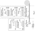
- FIG. 2 is a simplified illustration of initial stages in the fabrication of flexible patterned conductors in accordance with another preferred embodiment of the present invention.
- liquid polyimide 122 is preferably cast onto a layer of conductive foil 130 , typically of thickness 2.5-5 microns.
- the resulting polyimide layer is cured, preferably by heat as shown in step 134 , to provide a cured polyimide layer 140 , preferably of thickness 30-40 microns, on conductive foil 130 .
- a first surface 150 , of the cured polyimide layer 140 is subsequently subjected to surface conditioning, preferably including high pressure abrasion 154 , preferably performed by spraying, at high pressure, such as 30 psi, an abrading material, such as alumina, onto surface 150 .
- surface conditioning preferably including high pressure abrasion 154 , preferably performed by spraying, at high pressure, such as 30 psi, an abrading material, such as alumina, onto surface 150 .
- the abraded surface 150 preferably is rinsed with deionized water and thereafter, as shown at step 158 , is dried.
- FIG. 3 is a simplified illustration of further stages in the fabrication of flexible patterned conductors in accordance with preferred embodiments of the present invention.
- the stages shown in FIG. 3 follow the initial stages described hereinabove with reference to either of FIGS. 1 & 2 .
- a surface 200 of the conductive foil is scrubbed, at a step 202 , preferably by being mechanically abraded using an abrading material such as alumina slurry, which is preferably deposited onto surface 200 , and a roller 204 , preferably formed of polyvinyl acetate (PVA).
- an abrading material such as alumina slurry, which is preferably deposited onto surface 200
- a roller 204 preferably formed of polyvinyl acetate (PVA).
- the abraded surface 200 is cleaned using a surface cleaner, such as sodium hydroxide, which is preferably sprayed onto the abraded surface 200 , and a roller 206 , preferably formed of PVA, as shown in step 208 .
- the cleaned abraded surface 200 preferably is rinsed with deionized water as shown at step 212 and, as shown in step 214 , is dried.
- Step 250 includes deposition of photoresist layer 252 onto cleaned, abraded, rinsed and dried surface 200 , here designated by reference numeral 260 , of the conductive foil, here designated by reference numeral 270 , baking of the photoresist layer 252 and patterning exposure of photoresist layer 252 .
- the exposure employs a mask 272 , which fully covers generally only the conductive foil 270 , thereby allowing extremely accurate focus during exposure of photoresist layer 252 and thus extremely accurate patterning of photoresist layer 252 .
- Exposure is preferably followed by developing, at step 274 , the patterned photoresist layer 252 and baking of the developed patterned photoresist layer 252 , as shown in step 276 .
- Step 280 includes etching, at a step 282 , of those portions of conductive foil 270 underlying areas where the photoresist layer 252 was removed in the preceding photolithography patterning step 250 , rinsing, at a step 284 , of the etched conductive foil, preferably with deionized (DI) water, and drying, at a step 286 .
- DI deionized
- photoresist removal by scrubbing indicated generally as step 288 , preferably employing a mechanical scrubber 290 and a suitable solvent.
- Further cleaning indicated at step 292 , employs a detergent and a roller 294 .
- the cleaned patterned conductive foil surface 297 preferably is rinsed with deionized water 298 , and, as shown in step 299 , is dried.
- FIG. 4 is a simplified illustration of still further stages in the fabrication of flexible patterned conductors in accordance with preferred embodiments of the present invention.
- an epoxy emulsion 320 is provided over the cleaned product 310 , as shown in step 321 , the resulting emulsion layer 322 is baked, as shown in step 324 , and exposed, as shown in step 326 .
- the exposure employs a mask 328 , which fully covers generally only the conductive foil, thereby allowing extremely accurate focus during exposure and thus extremely accurate patterning of the emulsion layer 322 .
- the exposed emulsion layer 322 is developed at a step designated by reference numeral 330 and baked at a step designated by reference numeral 332 .
Landscapes
- Engineering & Computer Science (AREA)
- Microelectronics & Electronic Packaging (AREA)
- Manufacturing & Machinery (AREA)
- Physics & Mathematics (AREA)
- General Physics & Mathematics (AREA)
- Parts Printed On Printed Circuit Boards (AREA)
- Measurement Of Length, Angles, Or The Like Using Electric Or Magnetic Means (AREA)
- Manufacturing Of Printed Circuit Boards (AREA)
- Apparatuses And Processes For Manufacturing Resistors (AREA)
Abstract
Description
-
- surface conditioning of the flexible polyimide substrate using mechanical abrasion;
- scrubbing of the conductive foil prior to the patterning;
- removal of photoresist by scrubbing following the patterning;
- pressurized cleaning, using deionized water, following the patterning;
- automated algorithmic resistance calibration and shunt trimming; and
- forming an emulsion layer of epoxy over the conductive foil following the patterning.
-
- performing an initial resistance measurement;
- if a target resistance is reached, no shunt trimming is carried out;
- if the target resistance is not reached, trimming of a first shunt;
- if the target resistance is reached following the trimming of a first shunt, no further shunt trimming is carried out;
- if the target resistance is not reached following the trimming of the first shunt, automatically ascertaining whether the resistance change resulting from the trimming of a first shunt was as expected;
- if it is ascertained that the resistance change resulting from the trimming of a first shunt was not as expected, scrapping the strain gage or flexible polyimide-based resistor;
- if it is ascertained that the resistance change resulting from the trimming of a first shunt was as expected, trimming a second shunt;
- if the target resistance is reached following the trimming of a second shunt, no further shunt trimming is carried out;
- if the target resistance is not reached following trimming of the second shunt; automatically ascertaining whether the resistance change resulting from the trimming of a second shunt was as expected;
- if it is ascertained that the resistance change resulting from the trimming of a second shunt was not as expected, scrapping the strain gage or flexible polyimide-based resistor; and
- if it is ascertained that the resistance change resulting from trimming of the second shunt was as expected, trimming a third shunt.
Claims (17)
Applications Claiming Priority (2)
| Application Number | Priority Date | Filing Date | Title |
|---|---|---|---|
| IL275618A IL275618A (en) | 2020-06-23 | 2020-06-23 | Method of manufacture of a strain gage or flexible olyimide-based resistor |
| IL275618 | 2020-06-23 |
Publications (2)
| Publication Number | Publication Date |
|---|---|
| US20210396608A1 US20210396608A1 (en) | 2021-12-23 |
| US12123793B2 true US12123793B2 (en) | 2024-10-22 |
Family
ID=76730259
Family Applications (1)
| Application Number | Title | Priority Date | Filing Date |
|---|---|---|---|
| US17/352,909 Active 2042-10-14 US12123793B2 (en) | 2020-06-23 | 2021-06-21 | Method of manufacture of a strain gage or flexible polyimide-based resistor |
Country Status (6)
| Country | Link |
|---|---|
| US (1) | US12123793B2 (en) |
| EP (1) | EP3929528A3 (en) |
| JP (1) | JP2022003331A (en) |
| KR (1) | KR20210158337A (en) |
| CN (1) | CN113834417A (en) |
| IL (1) | IL275618A (en) |
Families Citing this family (1)
| Publication number | Priority date | Publication date | Assignee | Title |
|---|---|---|---|---|
| IL275618A (en) | 2020-06-23 | 2022-01-01 | Vishay Advanced Tech Ltd | Method of manufacture of a strain gage or flexible olyimide-based resistor |
Citations (8)
| Publication number | Priority date | Publication date | Assignee | Title |
|---|---|---|---|---|
| US5049232A (en) * | 1990-08-31 | 1991-09-17 | General Electric Company | Method of making diaphragm-type pressure transducers |
| JPH0438402A (en) | 1990-06-02 | 1992-02-07 | Kyowa Electron Instr Co Ltd | Strain gage and its manufacture |
| JP4758271B2 (en) | 2006-04-18 | 2011-08-24 | 株式会社共和電業 | Strain gauge for large strain measurement |
| US20170172687A1 (en) * | 2014-03-28 | 2017-06-22 | President And Fellows Of Harvard College | Printed Strain Gauges for Force Measurement |
| US20180217016A1 (en) * | 2015-09-29 | 2018-08-02 | Minebea Mitsumi Inc. | Strain gauge, load sensor, and method for manufacturing strain gauge |
| CN109000553A (en) * | 2018-06-04 | 2018-12-14 | 深圳市力合测控技术有限公司 | A kind of film-type strain gauge production method |
| JP2019066454A (en) | 2017-09-29 | 2019-04-25 | ミネベアミツミ株式会社 | Strain gauge and sensor module |
| EP3929528A2 (en) | 2020-06-23 | 2021-12-29 | Vishay Advanced Technologies, Ltd. | Method of manufacture of a strain gage or flexible polyimide-based resistor |
-
2020
- 2020-06-23 IL IL275618A patent/IL275618A/en unknown
-
2021
- 2021-06-09 EP EP21178550.6A patent/EP3929528A3/en not_active Withdrawn
- 2021-06-15 JP JP2021099715A patent/JP2022003331A/en active Pending
- 2021-06-21 CN CN202110684347.2A patent/CN113834417A/en active Pending
- 2021-06-21 US US17/352,909 patent/US12123793B2/en active Active
- 2021-06-21 KR KR1020210079921A patent/KR20210158337A/en not_active Withdrawn
Patent Citations (9)
| Publication number | Priority date | Publication date | Assignee | Title |
|---|---|---|---|---|
| JPH0438402A (en) | 1990-06-02 | 1992-02-07 | Kyowa Electron Instr Co Ltd | Strain gage and its manufacture |
| US5049232A (en) * | 1990-08-31 | 1991-09-17 | General Electric Company | Method of making diaphragm-type pressure transducers |
| JP4758271B2 (en) | 2006-04-18 | 2011-08-24 | 株式会社共和電業 | Strain gauge for large strain measurement |
| US20170172687A1 (en) * | 2014-03-28 | 2017-06-22 | President And Fellows Of Harvard College | Printed Strain Gauges for Force Measurement |
| US20180217016A1 (en) * | 2015-09-29 | 2018-08-02 | Minebea Mitsumi Inc. | Strain gauge, load sensor, and method for manufacturing strain gauge |
| JP2019066454A (en) | 2017-09-29 | 2019-04-25 | ミネベアミツミ株式会社 | Strain gauge and sensor module |
| CN109000553A (en) * | 2018-06-04 | 2018-12-14 | 深圳市力合测控技术有限公司 | A kind of film-type strain gauge production method |
| EP3929528A2 (en) | 2020-06-23 | 2021-12-29 | Vishay Advanced Technologies, Ltd. | Method of manufacture of a strain gage or flexible polyimide-based resistor |
| EP3929528A3 (en) | 2020-06-23 | 2022-03-30 | Vishay Advanced Technologies, Ltd. | Method of manufacture of a strain gage or flexible polyimide-based resistor |
Non-Patent Citations (1)
| Title |
|---|
| European Search Report dated Feb. 25, 2022 which issued during the prosecution of Applicant's European App No. 21178550.6. |
Also Published As
| Publication number | Publication date |
|---|---|
| JP2022003331A (en) | 2022-01-11 |
| EP3929528A3 (en) | 2022-03-30 |
| EP3929528A2 (en) | 2021-12-29 |
| IL275618A (en) | 2022-01-01 |
| KR20210158337A (en) | 2021-12-30 |
| US20210396608A1 (en) | 2021-12-23 |
| CN113834417A (en) | 2021-12-24 |
Similar Documents
| Publication | Publication Date | Title |
|---|---|---|
| CN107953672B (en) | Fluid ejection head and method of making fluid ejection head | |
| US12123793B2 (en) | Method of manufacture of a strain gage or flexible polyimide-based resistor | |
| JP2005521235A5 (en) | ||
| JPH05299720A (en) | Method for forming pattern of piezoelectric material | |
| JPH0719945B2 (en) | Method for manufacturing flexible circuit member | |
| US4288282A (en) | Method for producing a metallic pattern upon a substrate | |
| WO2026021121A1 (en) | Interdigital transducer and preparation method therefor, and surface acoustic wave filter | |
| US6620644B2 (en) | Method for manufacturing a thin-layer component, in particular a thin-layer high-pressure sensor | |
| JPH0580070A (en) | Strain gauge element and manufacture thereof | |
| US10538090B2 (en) | Method for manufacturing perforated substrate, method for manufacturing liquid ejection head, and method for detecting flaw | |
| AU2015344934B2 (en) | Mask for the manufacture of corrosion sensor | |
| JP2010169749A (en) | Methods for manufacturing photomask, method for manufacturing display, and apparatus for processing photomask substrate | |
| CN107256836B (en) | A kind of detection method of photoresist adhesion | |
| JPH09143761A (en) | Etching method and apparatus | |
| US20050260510A1 (en) | Method for determining the relative positional accuracy of two structure elements on a wafer | |
| US6511860B1 (en) | Method for manufacturing a thermopile on an electrically insulating substrate | |
| CN119595538A (en) | A packaging substrate and its ink bonding strength measurement method and preparation method | |
| KR100859640B1 (en) | Method for manufacturing test wafer for sining process of semiconductor manufacturing apparatus | |
| JPH05326395A (en) | Manufacture of semiconductor device | |
| CN120565531A (en) | A high-density frame structure and manufacturing method thereof | |
| JPH11150058A (en) | Method for measuring positional deviation and stress and x-ray mask | |
| JP2005303093A (en) | Heat treatment evaluation method and development processing evaluation method | |
| JP3404293B2 (en) | Method for manufacturing piezoelectric element | |
| JP2820008B2 (en) | Semiconductor device thickness monitoring structure and monitoring method | |
| CN118156128A (en) | An etching method for preventing non-aluminum segments from being corroded |
Legal Events
| Date | Code | Title | Description |
|---|---|---|---|
| FEPP | Fee payment procedure |
Free format text: ENTITY STATUS SET TO UNDISCOUNTED (ORIGINAL EVENT CODE: BIG.); ENTITY STATUS OF PATENT OWNER: LARGE ENTITY |
|
| AS | Assignment |
Owner name: VISHAY ADVANCED TECHNOLOGIES, LTD., ISRAEL Free format text: ASSIGNMENT OF ASSIGNORS INTEREST;ASSIGNORS:YARON, GILAD;HERCOWITZ, AMOS;MANOR, SHIRLEY;AND OTHERS;SIGNING DATES FROM 20210629 TO 20210704;REEL/FRAME:056758/0074 |
|
| STPP | Information on status: patent application and granting procedure in general |
Free format text: DOCKETED NEW CASE - READY FOR EXAMINATION |
|
| STPP | Information on status: patent application and granting procedure in general |
Free format text: NON FINAL ACTION MAILED |
|
| STPP | Information on status: patent application and granting procedure in general |
Free format text: RESPONSE TO NON-FINAL OFFICE ACTION ENTERED AND FORWARDED TO EXAMINER |
|
| STPP | Information on status: patent application and granting procedure in general |
Free format text: FINAL REJECTION MAILED |
|
| STPP | Information on status: patent application and granting procedure in general |
Free format text: RESPONSE AFTER FINAL ACTION FORWARDED TO EXAMINER |
|
| STPP | Information on status: patent application and granting procedure in general |
Free format text: NOTICE OF ALLOWANCE MAILED -- APPLICATION RECEIVED IN OFFICE OF PUBLICATIONS |
|
| ZAAB | Notice of allowance mailed |
Free format text: ORIGINAL CODE: MN/=. |
|
| STPP | Information on status: patent application and granting procedure in general |
Free format text: PUBLICATIONS -- ISSUE FEE PAYMENT VERIFIED |
|
| STCF | Information on status: patent grant |
Free format text: PATENTED CASE |
|
| AS | Assignment |
Owner name: VPG TECHNOLOGY DEVELOPMENT LTD., ISRAEL Free format text: ASSIGNMENT OF ASSIGNORS INTEREST;ASSIGNOR:VISHAY ADVANCED TECHNOLOGIES LTD.;REEL/FRAME:071746/0049 Effective date: 20250715 |