US12094530B2 - Josephson static random access memory - Google Patents
Josephson static random access memory Download PDFInfo
- Publication number
- US12094530B2 US12094530B2 US17/815,358 US202217815358A US12094530B2 US 12094530 B2 US12094530 B2 US 12094530B2 US 202217815358 A US202217815358 A US 202217815358A US 12094530 B2 US12094530 B2 US 12094530B2
- Authority
- US
- United States
- Prior art keywords
- superconducting
- loops
- josephson junction
- memory device
- control signals
- Prior art date
- Legal status (The legal status is an assumption and is not a legal conclusion. Google has not performed a legal analysis and makes no representation as to the accuracy of the status listed.)
- Active, expires
Links
- 230000003068 static effect Effects 0.000 title description 4
- 230000004907 flux Effects 0.000 claims abstract description 60
- 238000000034 method Methods 0.000 claims abstract description 46
- 230000005291 magnetic effect Effects 0.000 claims abstract description 30
- 230000004044 response Effects 0.000 claims abstract description 27
- 230000008569 process Effects 0.000 claims description 19
- 230000005540 biological transmission Effects 0.000 claims description 15
- 239000004744 fabric Substances 0.000 claims description 15
- 238000001816 cooling Methods 0.000 claims description 6
- 238000010586 diagram Methods 0.000 description 13
- 230000000694 effects Effects 0.000 description 5
- 238000005516 engineering process Methods 0.000 description 5
- 230000008878 coupling Effects 0.000 description 2
- 238000010168 coupling process Methods 0.000 description 2
- 238000005859 coupling reaction Methods 0.000 description 2
- 230000006870 function Effects 0.000 description 2
- 238000002955 isolation Methods 0.000 description 2
- 238000005259 measurement Methods 0.000 description 2
- 238000001208 nuclear magnetic resonance pulse sequence Methods 0.000 description 2
- 230000002085 persistent effect Effects 0.000 description 2
- 238000003860 storage Methods 0.000 description 2
- 230000006399 behavior Effects 0.000 description 1
- 230000008901 benefit Effects 0.000 description 1
- 239000003990 capacitor Substances 0.000 description 1
- 238000006243 chemical reaction Methods 0.000 description 1
- 239000004020 conductor Substances 0.000 description 1
- 230000001419 dependent effect Effects 0.000 description 1
- 239000006185 dispersion Substances 0.000 description 1
- 238000009826 distribution Methods 0.000 description 1
- 230000010354 integration Effects 0.000 description 1
- 238000001459 lithography Methods 0.000 description 1
- 238000004519 manufacturing process Methods 0.000 description 1
- 239000000463 material Substances 0.000 description 1
- 238000004806 packaging method and process Methods 0.000 description 1
- 238000013341 scale-up Methods 0.000 description 1
- 238000000638 solvent extraction Methods 0.000 description 1
- 239000002887 superconductor Substances 0.000 description 1
- 230000001360 synchronised effect Effects 0.000 description 1
Images





Classifications
-
- G—PHYSICS
- G11—INFORMATION STORAGE
- G11C—STATIC STORES
- G11C11/00—Digital stores characterised by the use of particular electric or magnetic storage elements; Storage elements therefor
- G11C11/21—Digital stores characterised by the use of particular electric or magnetic storage elements; Storage elements therefor using electric elements
- G11C11/44—Digital stores characterised by the use of particular electric or magnetic storage elements; Storage elements therefor using electric elements using super-conductive elements, e.g. cryotron
-
- G—PHYSICS
- G11—INFORMATION STORAGE
- G11C—STATIC STORES
- G11C19/00—Digital stores in which the information is moved stepwise, e.g. shift registers
- G11C19/32—Digital stores in which the information is moved stepwise, e.g. shift registers using super-conductive elements
-
- G—PHYSICS
- G11—INFORMATION STORAGE
- G11C—STATIC STORES
- G11C8/00—Arrangements for selecting an address in a digital store
- G11C8/16—Multiple access memory array, e.g. addressing one storage element via at least two independent addressing line groups
-
- H—ELECTRICITY
- H10—SEMICONDUCTOR DEVICES; ELECTRIC SOLID-STATE DEVICES NOT OTHERWISE PROVIDED FOR
- H10N—ELECTRIC SOLID-STATE DEVICES NOT OTHERWISE PROVIDED FOR
- H10N60/00—Superconducting devices
- H10N60/10—Junction-based devices
- H10N60/12—Josephson-effect devices
-
- H—ELECTRICITY
- H10—SEMICONDUCTOR DEVICES; ELECTRIC SOLID-STATE DEVICES NOT OTHERWISE PROVIDED FOR
- H10N—ELECTRIC SOLID-STATE DEVICES NOT OTHERWISE PROVIDED FOR
- H10N69/00—Integrated devices, or assemblies of multiple devices, comprising at least one superconducting element covered by group H10N60/00
Definitions
- This application relates to superconducting circuits.
- this application discloses a static random access memory (SRAM) implemented using a plurality of superconducting Josephson junctions (JJ) and related circuitry.
- SRAM static random access memory
- JJ superconducting Josephson junctions
- Such a memory may be configured to encode information in the form of magnetic flux quanta and may transfer such information based on single flux quantum (SFQ) pulses.
- SFQ single flux quantum
- Superconducting digital systems are capable of performing computing operations at clock speeds in excess of 100 GHz.
- the circuits comprise superconducting wires and Josephson junctions that together form superconducting loops in which information in the form of a single flux magnetic quantum is encoded and stored.
- the superconducting circuits can be configured to implement traditional logic gates such as AND gates, OR gates, Flip Flops, etc. These gates, in turn, can be configured to implement more complex logic such as shift registers, counters, processors, etc.
- JJ-based SRAM that: 1) is sufficiently fast and dense; 2) supports multiple read and write ports; and 3) can be fabricated in the same process/stackup as corresponding JJ-based logic circuits.
- a Josephson junction based memory device in a first aspect, includes a plurality of superconducting loops. Each superconducting loop includes at least one Josephson junction. The plurality of superconducting loops are electrically coupled. The plurality of superconducting loops includes a plurality of input loops, a plurality of readout loops, and at least one shared loop. The plurality of superconducting loops are configured to store or annihilate magnetic flux quanta in one or more of the superconducting loops in response to a combination of control signals and single flux quantum (SFQ) pulses.
- SFQ single flux quantum
- FIG. 1 illustrates a schematic diagram of a Josephson junction based memory device, in accordance with example embodiments.
- FIG. 2 A illustrates a write path sequence from the zero state to the one state utilizing the Josephson junction based memory device of FIG. 1 , in accordance with example embodiments.
- FIG. 2 B illustrates a write path sequence from the one state to the zero state utilizing the Josephson junction based memory device of FIG. 1 , in accordance with example embodiments.
- FIG. 3 A illustrates a read path sequence for reading a one state utilizing the Josephson junction based memory device of FIG. 1 , in accordance with example embodiments.
- FIG. 3 B illustrates a read path sequence for reading a zero state utilizing the Josephson junction based memory device of FIG. 1 , in accordance with example embodiments.
- FIG. 4 illustrates a circuit diagram of the Josephson junction based memory device of FIG. 1 , in accordance with example embodiments.
- FIG. 5 A illustrates a flux initialization process, in accordance with example embodiments.
- FIG. 5 C illustrates multiple unit cells sharing the same flux source, in accordance with example embodiments.
- FIG. 6 illustrates an array of unit cells arranged in a word-organized memory fabric, in accordance with example embodiments.
- FIG. 7 illustrates a wave-pipelining arrangement of the array of unit cells, in accordance with example embodiments.
- FIG. 8 illustrates an arrangement of partitioned subarrays, in accordance with example embodiments.
- FIG. 9 A illustrates a partitioned unit cell with separate write path and read path, in accordance with example embodiments.
- FIG. 9 B illustrates a unit cell with duplicated read paths, in accordance with example embodiments.
- FIG. 9 C illustrates a unit cell with duplicated write paths, in accordance with example embodiments.
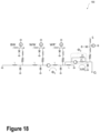
- FIG. 10 illustrates a schematic diagram of an alternative Josephson junction based memory device, in accordance with example embodiments.
- FIG. 11 A illustrates a read path sequence for reading a one state utilizing the alternative Josephson junction based memory device of FIG. 10 , in accordance with example embodiments.
- FIG. 11 B illustrates a read path sequence for reading a zero state utilizing the alternative Josephson junction based memory device of FIG. 10 , in accordance with example embodiments.
- FIG. 12 A illustrates a first read path variation utilizing the alternative Josephson junction based memory device of FIG. 10 , in accordance with example embodiments.
- FIG. 12 B illustrates a second read path variation utilizing the alternative Josephson junction based memory device of FIG. 10 , in accordance with example embodiments.
- FIG. 12 C illustrates a third read path variation utilizing the alternative Josephson junction based memory device of FIG. 10 , in accordance with example embodiments.
- FIG. 13 A illustrates a read path sequence for reading a one state utilizing the first read path variation of the alternative Josephson junction based memory device of FIG. 12 A , in accordance with example embodiments.
- FIG. 13 B illustrates a read path sequence for reading a zero state utilizing the first read path variation of the alternative Josephson junction based memory device of FIG. 12 A , in accordance with example embodiments.
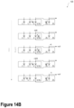
- FIG. 14 A illustrates a read path sequence for reading a one state utilizing the second read path variation of the alternative Josephson junction based memory device of FIG. 12 B , in accordance with example embodiments.
- FIG. 14 B illustrates a read path sequence for reading a zero state utilizing the second read path variation of the alternative Josephson junction based memory device of FIG. 12 B , in accordance with example embodiments.
- FIG. 15 A illustrates a read path sequence for reading a one state utilizing the third read path variation of the alternative Josephson junction based memory device of FIG. 12 C , in accordance with example embodiments.
- FIG. 15 B illustrates a read path sequence for reading a zero state utilizing the third read path variation of the alternative Josephson junction based memory device of FIG. 12 C , in accordance with example embodiments.
- FIG. 16 illustrates a circuit diagram of the first read path variation of the alternative Josephson junction based memory device of FIG. 12 A , in accordance with example embodiments.
- FIG. 17 illustrates a circuit diagram of the second read path variation of the alternative Josephson junction based memory device of FIG. 12 B , in accordance with example embodiments.
- FIG. 18 illustrates a circuit diagram of the third read path variation of the alternative Josephson junction based memory device of FIG. 12 C , in accordance with example embodiments.
- FIG. 19 illustrates a method, in accordance with example embodiments.
- any enumeration of elements, blocks, or steps in this specification or the claims is for purposes of clarity. Thus, such enumeration should not be interpreted to require or imply that these elements, blocks, or steps adhere to a particular arrangement or are carried out in a particular order.
- a coupled to B does not necessarily mean that items A and B are directly coupled to one another.
- a first component electrically coupled to a second component is interpreted to mean that the components are either directly coupled (e.g., via a conductor) or coupled to one another via one or more resistors, capacitors, inductors, and/or other active or passive components.
- the potential of superconducting digital technology as a beyond-CMOS technology derives from high energy efficiency, high computational density, and high interconnect bandwidth.
- the technology is based on the single-flux-quantum (SFQ) pulse, which is fast, low power, and low-dispersion/low-loss on superconductor transmission lines.
- SFQ single-flux-quantum
- Example embodiments involve various combinations of fabrication materials, density, power/clock distribution, logic and memory design, packaging, interfaces, and architecture.
- Logic devices based on such technologies are projected to have a computational density on par with leading-node CMOS based on an integration scale up 400 M JJ/cm 2 and a clock rate of 30 GHz.
- High performance logic requires on-chip memory that 1) is sufficiently fast and dense, 2) supports multiple read and write ports, and 3) can the fabricated in the same process/stackup as the logic.
- SRAM static random access memory
- JSRAM Josephson junction static random access memory
- X-Y addressing and readout is accomplished in JSRAM by moving stored SFQ between a series arrangement of adjacent superconducting loops.
- Conventional Josephson Transmission Line (JTL) interconnects provides high fan-out across the memory array.
- JTL Josephson Transmission Line
- the JSRAM design avoids exotic devices such as magnetics and so can be fabricated in the same process/stackup as that of high-performance SFQ logic. Furthermore, JSRAM utilizes the native SFQ logic signals and thus avoids the need for potentially complex conversion processes and hardware. The JSRAM design also avoids physically large components such as transformers, achieving a design density of 5 MB/cm 2 using 193i lithography. Wave pipelining allows throughput equal to the clock rate of the logic, with density that is a 500 ⁇ advance over conventional devices.
- FIG. 1 illustrates a schematic diagram of a Josephson junction based memory device 100 , in accordance with example embodiments.
- the Josephson junction based memory device 100 includes a plurality of superconducting loops 102 .
- Each superconducting loop e.g., superconducting loop 102 a , 102 b , 102 c , 102 d , or 102 e
- includes at least one Josephson junction e.g., Josephson junction 104 a , 104 b , 104 c , and/or 104 d ).
- the plurality of superconducting loops 102 are electrically coupled to one another.
- the plurality of superconducting loops 102 can include a plurality of input loops 110 and a plurality of readout loops 120 . As illustrated in FIG. 1 , the input loops 110 of a write path overlap with the readout loops 120 of a read path. That is, input loop 110 d and readout loop 120 a utilize the same superconducting loop, which can be termed as a “shared loop” (e.g., shared loop 130 ).
- shared loop e.g., shared loop 130
- the plurality of superconducting loops 102 could be electrically coupled in a series arrangement.
- the series arrangement can include five superconducting loops (e.g., superconducting loops 102 a , 102 b , 102 c , 102 d , and 102 e ), of which four are input loops (e.g., input loops 110 a , 110 b , 110 c , and 110 d ), two are readout loops (e.g., readout loops 120 a and 120 b ), and one is a shared loop (e.g., shared loop 130 ).
- each superconducting loop of the plurality of superconducting loops 102 has one or two adjacent loops.
- superconducting loop 102 a has one adjacent loop (superconducting loop 102 b )
- superconducting loop 102 b has two adjacent loops (superconducting loop 102 a and superconducting loop 102 c )
- superconducting loop 102 c has two adjacent loops (superconducting loop 102 b and superconducting loop 102 d )
- superconducting loop 102 d has two adjacent loops (superconducting loop 102 c and superconducting loop 102 e )
- superconducting loop 102 e has one adjacent loop (superconducting loop 102 d ). It will be understood that other arrangements of the superconducting loops 102 are possible and contemplated in relation to the present disclosure.
- the Josephson junction based memory device 100 also includes a plurality of address lines coupled to the plurality of superconducting loops 102 .
- each address line of the plurality of address lines 102 could include a Josephson transmission line and a current-bias source.
- the current-bias source may provide an AC signal corresponding to a global resonant clock network 170 , which may provide a system-wide clock to help enable operation in a synchronized manner.
- each address line of the plurality of address lines also includes a resistor connected between the Josephson transmission line and a corresponding superconducting loop of the plurality of superconducting loops 102 .
- the plurality of superconducting loops 102 are configured to store or annihilate magnetic flux quanta (e.g., SFQ 140 a or SFQ 140 b ) in one or more of the superconducting loops in response to a combination of control signals and single flux quantum (SFQ) pulses.
- SFQ 140 a or SFQ 140 b magnetic flux quanta
- control signals could be provided to the superconducting loops 102 by way of a bit write control line 160 , a word write control line 162 , a word read control line 164 , and/or a strobe control line 166 .
- the plurality of superconducting loops 102 are coupled to the global resonant clock network 170 .
- the plurality of superconducting loops 102 are configured to shift a magnetic flux quanta (e.g., SFQ 140 a ) from an initial superconducting loop (e.g., superconducting loop 102 c ) to an adjacent loop (e.g., superconducting loop 102 b ) in response to a SFQ pulse applied to the initial superconducting loop.
- a magnetic flux quanta e.g., SFQ 140 a
- the JSRAM write path involves moving a stored single-flux-quantum (SFQ) between superconducting loops separated by Josephson junctions (JJs), and the read path involves sensing the location of the stored SFQ.
- SFQ single-flux-quantum
- JJs Josephson junctions
- the operating principle involves addition of currents in the Josephson junctions (e.g., Josephson junctions 104 a , 104 b , 104 c , and 104 d ): a SFQ will move one stage to the left if a positive signal current adds constructively to the stored SFQ, which is a persistent current in the superconducting loop. Alternatively, the SFQ will move one loop to the right if a negative signal current adds to a negative current in the stored SFQ.
- a SFQ will move one stage to the left if a positive signal current adds constructively to the stored SFQ, which is a persistent current in the superconducting loop.
- the SFQ will move one loop to the right if a negative signal current adds to a negative current in the stored SFQ.
- the control signals for the write operation are Word Write (WW) and Bit Write (BW), with polarity indicated by (+) or ( ⁇ ). Note that Strobe (S) signals will pass through to the output (Q) irrespective of the state of the cell, if the state of the cell is not being readout.
- the plurality of superconducting loops 102 could be configured to provide information indicative of a presence of the magnetic flux quanta in one or more of the superconducting loops in response to a combination of control signals and SFQ pulses.
- FIG. 2 A illustrates a write path sequence 200 from the zero state to the one state utilizing the Josephson junction based memory device 100 of FIG. 1 , in accordance with example embodiments.
- write path sequence 200 shows the input SFQ pulse sequence needed to move from the zero state (e.g., SFQ stored in a third superconducting loop 102 c ) to the one state (e.g., SFQ stored in a second superconducting loop 102 b ).
- a positive signal current on the word write control line may act to shift the SFQ to the second superconducting loop (e.g., superconducting loop 102 b ).
- a magnetic flux quanta (e.g., SFQ 140 a ) stored in an initial superconducting loop can be shifted to an adjacent loop (e.g., superconducting loop 102 b ) in a first direction (e.g., left) along the series arrangement in response to a positive SFQ pulse polarity provided on the word write control line 162 .
- the magnetic flux quanta may be shifted from a superconducting loop (e.g., superconducting loop 102 b ) to an adjacent loop (e.g., superconducting loop 102 c ) in a second direction (e.g., right) along the series arrangement in response to a negative SFQ pulse polarity provided on the word write control line 162 .
- a superconducting loop e.g., superconducting loop 102 b
- an adjacent loop e.g., superconducting loop 102 c
- a second direction e.g., right
- FIG. 2 B illustrates a write path sequence 220 from the one state to the zero state utilizing the Josephson junction based memory device 100 of FIG. 1 , in accordance with example embodiments.
- write path sequence 220 shows the input SFQ pulse sequence needed to move from the one state (e.g., SFQ stored in a second superconducting loop 102 b ) to the zero state (e.g., SFQ stored in a third superconducting loop 102 c ).
- FIGS. 3 A and 3 B A detailed description of the read path for the memory device 100 is shown in FIGS. 3 A and 3 B .
- the design requires two clock cycles to complete a read operation, but a parallel write operation to a different cell during the second cycle may be additionally performed.
- the memory device 100 could provide and receive read control signals by way of the plurality of address lines to at least a portion of the plurality of superconducting loops 102 .
- the read control signals include word read, strobe, and output. The read path sequence of control signals is provided below.
- FIG. 3 A illustrates a read path sequence 300 for reading a one state utilizing the Josephson junction based memory device 100 of FIG. 1 , in accordance with example embodiments.
- Read path sequence 300 provides the Josephson junction switching sequence when reading a one state.
- the operating principle involves addition of currents in the Josephson junctions (e.g., Josephson junctions 104 a , 104 b , 104 c , and 104 d ): the SFQ will move one superconducting loop to the left if a positive signal current adds constructively to the stored SFQ, which is a persistent current in the loop.
- the SFQ will move one superconducting loop to the right if a negative signal current adds to negative current in the stored SFQ.
- the currents of SFQ stored in adjacent loops cancel in the shared JJ, so that two SFQ do not occupy a shared loop at the same time.
- the Q output is generated only if the S junction switches and moves the stored pulse between loops.
- the control signals for the read operation are Word Read (WR), Strobe (S), and output (Q) with polarity indicated by (+) or ( ⁇ ). Note that WR events must enclose S events. For AC-powered Josephson junctions where positive and negative pulses must occur in opposite halves of the clock cycle, this means that the pair of S events can complete within a clock cycle, but that a pair of WR events requires two clock cycles.
- FIG. 3 B illustrates a read path sequence 320 for reading a zero state utilizing the Josephson junction based memory device 100 of FIG. 1 , in accordance with example embodiments.
- Read path sequence 320 provides the Josephson junction switching sequence when reading a zero state.
- FIG. 4 illustrates a circuit diagram 400 of the Josephson junction based memory device 100 of FIG. 1 , in accordance with example embodiments.
- the circuit diagram 400 consists of standard Josephson transmission line (JTL) stages along the address lines.
- the current sources represent AC bias, which allows both positive and negative SFQ pulses to propagate at different times in the clock cycle.
- Resistors couple the inputs to the internals of the cell.
- Each junction-resistor pair is a decision-making element; if the signal current adds with the same polarity to the current of the SFQ in a storage loop as seen by the junction, the signal will trigger the junction to produce an SFQ pulse and move the stored pulse to the adjacent storage loop. Otherwise, the signal voltage will be lost across the resistor.
- the pulsed voltage sources represent SFQ sources to produce the initial state.
- the initial state shown corresponds to the zero state, but other initial states could be used.
- the current sources represent the ac bias supplied by the global resonant clock network on-chip. Phasing of the bias sources is provided to be consistent with the desired SFQ pulse timing.
- FIG. 5 A illustrates a flux initialization process 500 , in accordance with example embodiments.
- both SFQs may be initialized into the rightmost loop of the unit cell so that there is only a single transformer.
- the current required in the primary depends on the desired flux and the mutual inductance M according to:
- a second step of flux initialization process 520 once the secondary loop has reached a superconducting critical temperature, the control current is turned off and an exact integer number N of SFQ becomes set up in the loop, with the number of SFQs being determined by the initial current in the primary according to:
- I primary ⁇ M ⁇ N ⁇ ⁇ 0 M .
- the memory device 100 may include at least one magnetically coupled control line.
- the plurality of superconducting loops 102 are configured to provide an initial flux state in response to a two-step flux initialization process.
- the two-step flux initialization process includes: 1) while cooling down the Josephson junction based memory device, providing an initialization signal via the at least one magnetically coupled control line; and 2) upon reaching a superconducting critical temperature of the Josephson junction based memory device, turning off the initialization signal such that an exact integral number of SFQ are stored in one or more of the superconducting loops.
- FIG. 5 C illustrates a scenario 530 in which multiple unit cells (e.g., respective unit cells associated with inductor 532 and inductor 534 ) share the same flux source (e.g., flux source 536 ), in accordance with example embodiments.
- the mutual inductance L′ shared by the loops is much less than the total inductance L of each loop. In such scenarios, a low L′ inductance achieves good isolation by approximating a low-impedance source.
- FIG. 6 illustrates an array of unit cells arranged in a word-organized memory fabric 600 , in accordance with example embodiments.
- the address lines use Josephson Transmission Lines (JTLs)
- the memory fabric is wave-pipelined, and multiple operations can be in flight at once. It is not allowed to read and write to the same word in the same clock cycle, but simultaneous read and write to different words is allowed.
- the unit cells may be arrayed to produce a word-organized memory fabric.
- the address lines use JTLs that fan-out the signals to all cells in a vine configuration.
- the series arrangement e.g., Josephson junction based memory device 100
- An array of coupled unit cells could form a memory fabric, which can be wave-pipelined. In such scenarios, multiple operations can be carried out simultaneously across the memory fabric.
- the unit cells of the memory fabric 600 are coupled to a global resonant clock network (e.g., global resonant clock network 170 ).
- FIG. 7 illustrates a wave-pipelining arrangement 700 of the array of unit cells, in accordance with example embodiments.
- Wave-pipelining through the array means that the phasing of the AC bias sources will advance with signal latency. In this way, multiple operations may be in flight simultaneously, achieving throughput at the native clock frequency of the logic.
- FIG. 7 supposes that a local group of unit cells requires four of eight clock phases (e.g. 0, 2, 4, and 6) and that these phases precess from top-left to bottom-right. This is consistent with the signal propagation from top-left to bottom-right along Manhattan-geometry paths.
- FIG. 8 illustrates an arrangement 800 of partitioned subarrays, in accordance with example embodiments.
- partitioning the array of unit cells into smaller active subarrays interconnected with passive transmission lines can improve latency and improve power dissipation, as high activity factor of the junctions during a read or write operation is restricted to the subarray.
- FIG. 9 A illustrates a partitioned unit cell 900 with separate write path and read path, in accordance with example embodiments.
- FIG. 9 B illustrates a partitioned unit cell 920 with duplicated read paths, in accordance with example embodiments.
- the read path is duplicated to make two read ports.
- the stored SFQ associated with the write path can be communicated to the read path through a Josephson junction transmission line splitter network that provides isolation and gain.
- FIG. 10 illustrates a schematic diagram of an alternative Josephson junction based memory device 1000 , in accordance with example embodiments.
- the series arrangement may include four superconducting loops, of which all are input loops.
- the alternative memory device 1000 could include a readout stage 1002 .
- the readout stage 1002 could be coupled to a Josephson junction 1004 shared by two of the input loops.
- the readout stage 1002 is configured to detect whether an SFQ is stored in a specific one of the input loops.
- the readout stage is connected to the rightmost junction of the input loops, and detects whether the stored pulse is in the rightmost loop during read operations.
- One potential advantage of the design of the alternative memory device 1000 is that it supports single-cycle reads, as illustrated and described in FIGS. 11 A and 11 B .
- FIG. 11 A illustrates a read path sequence 1100 for reading a one state utilizing the alternative Josephson junction based memory device 1000 of FIG. 10 , in accordance with example embodiments.
- the S input produces the Q output unless the stored pulse is in the rightmost loop.
- the pair of WR events and the pair of S events can all complete within a clock cycle, in contrast to the design of memory device 100 .
- FIGS. 12 A, 12 B, and 12 C Three functionally equivalent read paths conforming to the second design (e.g., alternative memory device 1000 ) are shown in FIGS. 12 A, 12 B, and 12 C . It will be understood that while three alternative read path variations are described, other alternatives are possible and contemplated.
- FIG. 12 A illustrates a first read path variation 1200 utilizing the alternative Josephson junction based memory device 1000 of FIG. 10 , in accordance with example embodiments. Relative inductance of the different loops is shown. Approximate inductor values are shown for illustration, neglecting second-order effects such as JJ inductance and leakage between loops.
- FIG. 12 B illustrates a second read path variation 1220 utilizing the alternative Josephson junction based memory device 1000 of FIG. 10 , in accordance with example embodiments. Relative inductance of the different loops is shown. Approximate inductor values are shown for illustration, neglecting second-order effects such as JJ inductance and leakage between loops.
- FIG. 12 C illustrates a third read path variation 1230 utilizing the alternative Josephson junction based memory device 1000 of FIG. 10 , in accordance with example embodiments. Relative inductance of the different loops is shown. Approximate inductor values are shown for illustration, neglecting second-order effects such as JJ inductance and leakage between loops.
- the read path sequences for the first, second, and third read path variations are provided in FIGS. 13 A, 13 B, 14 A, 14 B, 15 A, and 15 B .
- FIG. 13 B illustrates a read path sequence 1320 for reading a zero state utilizing the first read path variation 1200 of the alternative Josephson junction based memory device 1000 of FIG. 12 A , in accordance with example embodiments.
- the ⁇ WR signal moves the SFQ from the input stages into the two 2L loops.
- FIG. 15 A illustrates a read path sequence 1500 for reading a one state utilizing the third read path variation 1230 of the alternative Josephson junction based memory device 1000 of FIG. 12 C , in accordance with example embodiments.
- FIG. 15 B illustrates a read path sequence 1520 for reading a zero state utilizing the third read path variation 1230 of the alternative Josephson junction based memory device 1000 of FIG. 12 C , in accordance with example embodiments.
- the ⁇ WR signal when reading a zero, the ⁇ WR signal reverses the polarity of the half-SFQ in the loop connected to the input stages.
- FIG. 16 illustrates a circuit diagram 1600 of the first read path variation 1200 of the alternative Josephson junction based memory device 1000 of FIG. 12 A , in accordance with example embodiments.
- FIG. 17 illustrates a circuit diagram 1700 of the second read path variation 1220 of the alternative Josephson junction based memory device 1000 of FIG. 12 B , in accordance with example embodiments.
- FIG. 18 illustrates a circuit diagram 1800 of the third read path variation 1230 of the alternative Josephson junction based memory device 1000 of FIG. 12 C , in accordance with example embodiments.
- the 1 ⁇ 2 SFQ in the inductor loop of inductance L is implemented as two inductors in parallel, each of inductance 2L, with a full SFQ applied to one of the two inductors.
- FIG. 19 illustrates a method 1900 , in accordance with example embodiments.
- the method 1900 includes a process for storing digital information in a Josephson junction based memory device (e.g., memory device 100 or memory device 1000 as illustrated and described in relation to FIGS. 1 and 10 ).
- a Josephson junction based memory device e.g., memory device 100 or memory device 1000 as illustrated and described in relation to FIGS. 1 and 10 .
- the method 1900 includes providing, to a plurality of superconducting loops (e.g., superconducting loops 102 ), a combination of control signals and single flux quantum (SFQ) pulses.
- Each superconducting loop comprises at least one Josephson junction (e.g., Josephson junctions 104 a , 104 b , 104 c , and 104 d ).
- the plurality of superconducting loops are electrically coupled.
- the plurality of superconducting loops include a plurality of input loops (e.g., input loops 110 ), a plurality of readout loops (e.g., readout loops 120 ), and at least one shared loop (e.g., shared loop 130 ).
- the method 1900 includes, in response to the combination of control signals and SFQ pulses, storing or annihilating magnetic flux quanta (e.g., SFQ 140 a and/or 140 b ) in one or more of the superconducting loops.
- SFQ 140 a and/or 140 b magnetic flux quanta
- Method 1900 may additionally include, in response to an SFQ pulse being applied to an initial superconducting loop of the plurality of superconducting loops, shifting a magnetic flux quanta from the initial superconducting loop to an adjacent loop.
- the Josephson junction based memory device may include a plurality of address lines coupled to the plurality of superconducting loops.
- each address line of the plurality of address lines may include a Josephson transmission line and a current-bias source.
- the current-bias source provides an AC signal corresponding to a global resonant clock network (e.g., global resonant clock network 170 ).
- control signals may include write control signals. wherein the plurality of address lines are configured to provide the write control signals to at least a portion of the plurality of superconducting loops.
- the write control signals include word write (WW) and bit write (BW).
- control signals may additionally include read control signals.
- the plurality of address lines are configured to provide the read control signals to at least a portion of the plurality of superconducting loops.
- the read control signals include word read (WR), strobe (S) and output.
- the method 1900 may also include, while cooling down the Josephson junction based memory device, providing an initialization signal via an at least one magnetically coupled control line.
- the method 1900 may additionally include, upon reaching a superconducting critical temperature of the Josephson junction based memory device, turning off the initialization signal such that an exact integral number of SFQ are stored in the plurality of superconducting loops.
- Embodiments of the present disclosure may thus relate to one of the enumerated example embodiments (EEEs) listed below.
- EEE 1 includes a Josephson junction based memory device comprising:
- EEE 2 includes the Josephson junction based memory device of EEE 1, wherein the plurality of superconducting loops are electrically coupled in a series arrangement, wherein each superconducting loop of the plurality of superconducting loops has one or two adjacent loops.
- EEE 3 includes the Josephson junction based memory device of EEE 2, wherein the plurality of superconducting loops are configured to shift a magnetic flux quanta from an initial superconducting loop to an adjacent loop in response to a SFQ pulse applied to the initial superconducting loop.
- EEE 4 includes the Josephson junction based memory device of EEE 3, wherein the magnetic flux quanta is shifted from an initial superconducting loop to an adjacent loop in a first direction along the series arrangement in response to a positive SFQ pulse polarity, and wherein the magnetic flux quanta is shifted from an initial superconducting loop to an adjacent loop in a second direction along the series arrangement in response to a negative SFQ pulse polarity.
- EEE 5 includes the Josephson junction based memory device of EEE 2, wherein the series arrangement comprises five superconducting loops, of which four are input loops, two are readout loops, and one is a shared loop.
- EEE 6 includes the Josephson junction based memory device of EEE 2, further comprising a readout stage, wherein the series arrangement comprises four superconducting loops, of which all are input loops, wherein the readout stage is coupled to a Josephson junction of one of the input loops, wherein the readout stage is configured to detect whether an SFQ is stored in a specific one of the input loops.
- EEE 7 includes the Josephson junction based memory device of EEE 2, wherein the series arrangement comprises a unit cell, wherein the Josephson junction based memory device comprises an array of unit cells that forms a memory fabric, wherein the memory fabric is wave-pipelined, and where multiple operations can be carried out simultaneously across the memory fabric.
- EEE 8 includes the Josephson junction based memory device of EEE 7, wherein the unit cells of the memory fabric are coupled to a global resonant clock network.
- EEE 9 includes the Josephson junction based memory device of EEE 1, further comprising a plurality of address lines coupled to the plurality of superconducting loops, wherein each address line of the plurality of address lines comprises:
- EEE 10 includes the Josephson junction based memory device of EEE 9, wherein each address line of the plurality of address lines further comprises a resistor connected between the Josephson transmission line and a corresponding superconducting loop of the plurality of superconducting loops.
- EEE 11 includes the Josephson junction based memory device of EEE 9, wherein the control signals comprise write control signals, wherein the plurality of address lines are configured to provide the write control signals to at least a portion of the plurality of superconducting loops, wherein the write control signals comprise:
- EEE 12 includes the Josephson junction based memory device of EEE 9, wherein the plurality of superconducting loops are further configured to provide information indicative of a presence of the magnetic flux quanta in the one or more of the superconducting loops in response to a combination of control signals and SFQ pulses.
- EEE 13 includes the Josephson junction based memory device of EEE 9, wherein the control signals comprise read control signals, wherein the plurality of address lines are configured to provide the read control signals to at least a portion of the plurality of superconducting loops, wherein the read control signals comprise:
- EEE 14 includes the Josephson junction based memory device of EEE 1, further comprising at least one magnetically coupled control line, wherein the plurality of superconducting loops are further configured to provide an initial flux state in response to a two-step flux initialization process, wherein the two-step flux initialization process comprises:
- EEE 15 includes a method for storing digital information in a Josephson junction based memory device comprising:
- EEE 16 includes the method of EEE 15, further comprising:
- EEE 17 includes the method of EEE 15, wherein the Josephson junction based memory device comprises a plurality of address lines coupled to the plurality of superconducting loops, wherein each address line of the plurality of address lines comprises:
- EEE 18 includes the method of EEE 17, wherein the control signals comprise write control signals, wherein the plurality of address lines are configured to provide the write control signals to at least a portion of the plurality of superconducting loops, wherein the write control signals comprise:
- EEE 19 includes the method of EEE 17, wherein the control signals comprise read control signals, wherein the plurality of address lines are configured to provide the read control signals to at least a portion of the plurality of superconducting loops, wherein the read control signals comprise:
- EEE 20 includes the method of EEE 15, further comprising:
Landscapes
- Engineering & Computer Science (AREA)
- Computer Hardware Design (AREA)
- Microelectronics & Electronic Packaging (AREA)
- Superconductor Devices And Manufacturing Methods Thereof (AREA)
- Shift Register Type Memory (AREA)
Priority Applications (5)
| Application Number | Priority Date | Filing Date | Title |
|---|---|---|---|
| US17/815,358 US12094530B2 (en) | 2022-07-27 | 2022-07-27 | Josephson static random access memory |
| CN202380057386.7A CN120019437A (zh) | 2022-07-27 | 2023-07-24 | 约瑟夫森静态随机存取存储器 |
| JP2025504374A JP2025532459A (ja) | 2022-07-27 | 2023-07-24 | ジョセフソンスタティックランダムアクセスメモリ |
| PCT/US2023/028456 WO2025034194A2 (en) | 2022-07-27 | 2023-07-24 | Josephson static random access memory |
| EP23943945.8A EP4562633A2 (de) | 2022-07-27 | 2023-07-24 | Statischer josephson-direktzugriffsspeicher |
Applications Claiming Priority (1)
| Application Number | Priority Date | Filing Date | Title |
|---|---|---|---|
| US17/815,358 US12094530B2 (en) | 2022-07-27 | 2022-07-27 | Josephson static random access memory |
Publications (2)
| Publication Number | Publication Date |
|---|---|
| US20240038298A1 US20240038298A1 (en) | 2024-02-01 |
| US12094530B2 true US12094530B2 (en) | 2024-09-17 |
Family
ID=89664762
Family Applications (1)
| Application Number | Title | Priority Date | Filing Date |
|---|---|---|---|
| US17/815,358 Active 2042-09-19 US12094530B2 (en) | 2022-07-27 | 2022-07-27 | Josephson static random access memory |
Country Status (5)
| Country | Link |
|---|---|
| US (1) | US12094530B2 (de) |
| EP (1) | EP4562633A2 (de) |
| JP (1) | JP2025532459A (de) |
| CN (1) | CN120019437A (de) |
| WO (1) | WO2025034194A2 (de) |
Families Citing this family (2)
| Publication number | Priority date | Publication date | Assignee | Title |
|---|---|---|---|---|
| WO2025207761A1 (en) * | 2024-03-26 | 2025-10-02 | William Robert Reohr | Superconducting retention memory with non-superconducting write circuit |
| WO2026072066A1 (en) * | 2024-09-30 | 2026-04-02 | IMEC USA NANOELECTRONICS DESIGN CENTER, Inc. | Josephson crossbar switch fabric |
Citations (6)
| Publication number | Priority date | Publication date | Assignee | Title |
|---|---|---|---|---|
| JPH056345A (ja) * | 1991-06-27 | 1993-01-14 | Oki Electric Ind Co Ltd | 系制御システム |
| US8571614B1 (en) * | 2009-10-12 | 2013-10-29 | Hypres, Inc. | Low-power biasing networks for superconducting integrated circuits |
| US20180101786A1 (en) * | 2016-10-06 | 2018-04-12 | D-Wave Systems Inc. | Quantum flux parametron based structures (e.g., muxes, demuxes, shift registers), addressing lines and related methods |
| US20190362780A1 (en) * | 2018-05-25 | 2019-11-28 | Microsoft Technology Licensing, Llc | Memory system with signals on read lines not phase-aligned with josephson transmission line (jtl) elements included in the write lines |
| US10777263B1 (en) | 2019-04-23 | 2020-09-15 | Northrop Grumman Systems Corporation | Josephson memory and logic circuits using quasi-long-junction interconnect |
| US11476842B1 (en) * | 2021-06-17 | 2022-10-18 | Northrop Grumman Systems Corporation | Superconducting current source system |
Family Cites Families (1)
| Publication number | Priority date | Publication date | Assignee | Title |
|---|---|---|---|---|
| US5233244A (en) * | 1991-03-25 | 1993-08-03 | Fujitsu Limited | Josephson logic gate having a plurality of input ports and a josephson logic circuit that uses such a josephson logic gate |
-
2022
- 2022-07-27 US US17/815,358 patent/US12094530B2/en active Active
-
2023
- 2023-07-24 JP JP2025504374A patent/JP2025532459A/ja active Pending
- 2023-07-24 CN CN202380057386.7A patent/CN120019437A/zh active Pending
- 2023-07-24 WO PCT/US2023/028456 patent/WO2025034194A2/en not_active Ceased
- 2023-07-24 EP EP23943945.8A patent/EP4562633A2/de active Pending
Patent Citations (7)
| Publication number | Priority date | Publication date | Assignee | Title |
|---|---|---|---|---|
| JPH056345A (ja) * | 1991-06-27 | 1993-01-14 | Oki Electric Ind Co Ltd | 系制御システム |
| US8571614B1 (en) * | 2009-10-12 | 2013-10-29 | Hypres, Inc. | Low-power biasing networks for superconducting integrated circuits |
| US20180101786A1 (en) * | 2016-10-06 | 2018-04-12 | D-Wave Systems Inc. | Quantum flux parametron based structures (e.g., muxes, demuxes, shift registers), addressing lines and related methods |
| US20190362780A1 (en) * | 2018-05-25 | 2019-11-28 | Microsoft Technology Licensing, Llc | Memory system with signals on read lines not phase-aligned with josephson transmission line (jtl) elements included in the write lines |
| US10777263B1 (en) | 2019-04-23 | 2020-09-15 | Northrop Grumman Systems Corporation | Josephson memory and logic circuits using quasi-long-junction interconnect |
| US10902908B2 (en) | 2019-04-23 | 2021-01-26 | Northrop Grumman Systems Corporation | Josephson memory and logic circuits using quasi-long-junction interconnect |
| US11476842B1 (en) * | 2021-06-17 | 2022-10-18 | Northrop Grumman Systems Corporation | Superconducting current source system |
Non-Patent Citations (5)
| Title |
|---|
| Braiman, Yehuda, N. Nair, J. Rezac, and Neena Imam. "Memory cell operation based on small Josephson junctions arrays." Superconductor Science and Technology 29, No. 12 (2016): 124003. |
| Burnett, Randall, Ryan Clarke, Timothy Lee, Harold Hearne, Jacob Vogel, Quentin Herr, and Anna Herr. "Demonstration of superconducting memory for an RQL CPU." In Proceedings of the International Symposium on Memory Systems, pp. 321-323. 2018. |
| Castellano, Maria Gabriella, Fabio Chiarello, Guido Torrioli, and Pasquale Carelli. "Static flux bias of a flux qubit using persistent current trapping." Superconductor Science and Technology 19, No. 11 (2006): 1158. |
| Polonsky, S. V., A. F. Kirichenko, V. K. Semenov, and K. K. Likharev. "Rapid single flux quantum random access memory." IEEE Transactions on Applied Superconductivity 5, No. 2 (1995): 3000-3005. |
| Silver, A., R. Phillips, and R. Sandell. "High speed non-latching SQUID binary ripple counter." IEEE Transactions on Magnetics 21, No. 2 (1985): 204-207. |
Also Published As
| Publication number | Publication date |
|---|---|
| CN120019437A (zh) | 2025-05-16 |
| JP2025532459A (ja) | 2025-10-01 |
| EP4562633A2 (de) | 2025-06-04 |
| US20240038298A1 (en) | 2024-02-01 |
| WO2025034194A2 (en) | 2025-02-13 |
| WO2025034194A9 (en) | 2025-05-15 |
| WO2025034194A3 (en) | 2025-04-10 |
Similar Documents
| Publication | Publication Date | Title |
|---|---|---|
| US11159168B2 (en) | Superconducting non-destructive readout circuits | |
| US10923646B2 (en) | Superconducting switch having a persistent and a non-persistent state | |
| EP3374995B1 (de) | Josephson-magnet-direktzugriffsspeicher mit einem induktiven shunt | |
| US9595970B1 (en) | Superconducting cell array logic circuit system | |
| US9712172B2 (en) | Devices with an array of superconducting logic cells | |
| US10331163B1 (en) | Superconducting integrated circuits with clock signals distributed via inductive coupling | |
| US20240038298A1 (en) | Josephson Static Random Access Memory | |
| CA3108435A1 (en) | Quantizing loop memory cell system | |
| EP3766069B1 (de) | Supraleitendes speichersystem mit gestapelten treibern und differentialtransformatoren | |
| KR102599221B1 (ko) | 조셉슨 전류원 시스템 | |
| Bairamkulov et al. | Superconductive electronics: A 25-year review [feature] | |
| WO2019226379A1 (en) | Current-based superconductor memory cell and methods | |
| EP3915113A1 (de) | Verwendung einer magnetischen josephson-übergang-vorrichtung als pi-inverter | |
| Silver et al. | A new concept for ultra-low power and ultra-high clock rate circuits | |
| WO2025207761A1 (en) | Superconducting retention memory with non-superconducting write circuit | |
| US3056041A (en) | Cryogenic shift register utilizing current source feeding series-connected stage-chain with parallel paths in each stage | |
| WO2026072064A1 (en) | Josephson d-latch | |
| WO2026072066A1 (en) | Josephson crossbar switch fabric | |
| Van Duzer | Challenges in the Realization of SFQ Digital Circuits | |
| Mladenov | RSFQ DC to SFQ converter with reduced Josephson current density |
Legal Events
| Date | Code | Title | Description |
|---|---|---|---|
| FEPP | Fee payment procedure |
Free format text: ENTITY STATUS SET TO UNDISCOUNTED (ORIGINAL EVENT CODE: BIG.); ENTITY STATUS OF PATENT OWNER: LARGE ENTITY |
|
| AS | Assignment |
Owner name: IMEC VZW, BELGIUM Free format text: ASSIGNMENT OF ASSIGNORS INTEREST;ASSIGNORS:LUO, HENRY;HERR, ANNA YURIEVNA;HERR, QUENTIN PAUL;SIGNING DATES FROM 20220729 TO 20220927;REEL/FRAME:061242/0214 |
|
| STPP | Information on status: patent application and granting procedure in general |
Free format text: NON FINAL ACTION MAILED |
|
| STPP | Information on status: patent application and granting procedure in general |
Free format text: RESPONSE TO NON-FINAL OFFICE ACTION ENTERED AND FORWARDED TO EXAMINER |
|
| STPP | Information on status: patent application and granting procedure in general |
Free format text: NOTICE OF ALLOWANCE MAILED -- APPLICATION RECEIVED IN OFFICE OF PUBLICATIONS |
|
| STPP | Information on status: patent application and granting procedure in general |
Free format text: PUBLICATIONS -- ISSUE FEE PAYMENT VERIFIED |
|
| STCF | Information on status: patent grant |
Free format text: PATENTED CASE |