EP3374995B1 - Josephson-magnet-direktzugriffsspeicher mit einem induktiven shunt - Google Patents
Josephson-magnet-direktzugriffsspeicher mit einem induktiven shunt Download PDFInfo
- Publication number
- EP3374995B1 EP3374995B1 EP16795516.0A EP16795516A EP3374995B1 EP 3374995 B1 EP3374995 B1 EP 3374995B1 EP 16795516 A EP16795516 A EP 16795516A EP 3374995 B1 EP3374995 B1 EP 3374995B1
- Authority
- EP
- European Patent Office
- Prior art keywords
- bit
- memory
- lines
- state
- line
- Prior art date
- Legal status (The legal status is an assumption and is not a legal conclusion. Google has not performed a legal analysis and makes no representation as to the accuracy of the status listed.)
- Active
Links
Images



Classifications
-
- G—PHYSICS
- G11—INFORMATION STORAGE
- G11C—STATIC STORES
- G11C11/00—Digital stores characterised by the use of particular electric or magnetic storage elements; Storage elements therefor
- G11C11/21—Digital stores characterised by the use of particular electric or magnetic storage elements; Storage elements therefor using electric elements
- G11C11/44—Digital stores characterised by the use of particular electric or magnetic storage elements; Storage elements therefor using electric elements using super-conductive elements, e.g. cryotron
Definitions
- CMOS complimentary metal-oxide semiconductor
- US3164808 teaches a method and system in relation to information handling arrangements, and more particularly to improvements in information storage arrangements of the kind utilizing superconductive elements.
- a changing phase difference in time of the phase of the superconducting electron wave-function between the two superconductors corresponds to a potential difference between the two superconductors.
- the SIS type of junction may be part of a superconducting loop.
- the magnetic flux through the loop changes by an integer multiple of a single quantum of magnetic flux.
- the voltage pulse associated with the single quantum of magnetic flux is referred to as a single-flux-quantum (SFQ) pulse.
- SFQ single-flux-quantum
- overdamped Josephson junctions can create individual single-flux-quantum (SFQ) pulses.
- each Josephson junction may be part of one or more superconducting loops. The phase difference across the junction may be modulated by the magnetic flux applied to the loop.
- non-latching SQUIDs When the read word-line signal is removed, the non-latching SQUIDs may revert back to a zero voltage state.
- the use of non-latching SQUIDs may have some limitations, including, for example, the voltage produced by the SQUID may be affected by variations in: (1) the critical currents of the Josephson junctions used as part of the SQUID, (2) the inductance of the SQUID, (3) the flux bias applied to the memory cells, and (4) the bias current supplied to the column of the memory cells.
- the principles of physics may limit the voltage to approximately 200 micro-volts. That in turn, may drive the transmission line impedance to approximately 20 ohms to ensure sufficient current to the sense amplifiers.
- the lower impedance may require additional capacitance, which in turn, may increase the footprint of the memory system and thereby reduce the data storage capacity of the memory.
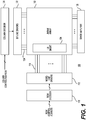
- Word-line drivers 112 may provide such current via word-lines 114.
- Word-lines 114 may include both read word-lines and write word-lines. In other words, different word-lines may be used to provide current to the selected memory cells for read or write operations.
- Memory system 100 may further include column decoder 120 that may be configured to decode column control/address signals. Column decoder 120 may further be coupled to bit-line drivers 122.
- Bit-line drivers 122 may include circuitry to provide bit-line read current to a subset or all of the memory cells associated with a selected bit-line for any read or write operations. Bit-line drivers 122 may provide such current via bit-lines 124.
- Bit-lines 124 may include both read bit-lines and write bit-lines.
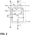
- MJJ device 220 may be a superconductor with at least two magnetic barrier layers (e.g., ferromagnetic barriers) that are compatible with single flux quantum (SFQ) pulse-based circuits.
- SFQ single flux quantum
- a superconductor-insulator-superconductor (SIS) type device discussed earlier may be modified to be a SIS/ferromagnetic-superconductor (SIS/FS) type of device.
- memory cell 200 may be coupled to word-lines and bit-lines for performing various memory operations, including, for example read and write operations.
- a read word-line (RWL) for performing a read operation may be coupled to memory cell 200.
- a write word-line (WWL) for performing a write operation may be coupled to memory cell 200.
- a read bit-line (RBL) for performing a read operation may be coupled to memory cell 200.
- a write bit-line (WBL) for performing a write operation may also be coupled to memory cell 200.
- Each of the word-lines may be one of the word-lines 114 of FIG. 1 .
- each of the bit-lines may be one of the bit-lines 124 of FIG. 1 .
- the write bit-line may be magnetically coupled (via coupling 240) to MJJ 220.
- coupling 240 with MJJ 220 may be such that a magnetic field generated by at least one of the magnetic barrier layers of MJJ 220 can be changed by the application of a local read word-line current and/or by the application of a local bit-line current.
- the write word-line may be magnetically coupled (via coupling 250) to MJJ 220.
- coupling 250 with MJJ 220 may be such that a magnetic field generated by at least one of the magnetic barrier layers of the MJJ can be changed by the application of a local write word-line current and/or by the application of a write bit-line current.
- this state may be the " ⁇ state.”
- MJJ 220 may apply flux to JJs 212 and 214 such that under the application of a word read current via inductors 230 and 232 the induced currents, in memory storage element 210, due to the flux generated by MJJ 220 and by the coupling of the word-read current to inductors 216 and 218, may combine with a bit-read current applied at node A to trigger the Josephson junctions 212 and 214 into a 2.5 millivolts state.
- This voltage may generate a current along the read bit-line, which may act as a transmission line with a certain impedance. This current may be sensed using a sense amplifier.
- the flux generated as a result of the current flowing through the local read word-line may not be enough to drive the readout SQUID into a voltage state.
- the change in an output voltage, current, or any other parameter of memory storage element 210 may be sensed using a sense amplifier (e.g., sense amplifier 130 of FIG. 1 ).
- the presence or absence of a current pulse, once amplified by the sense amplifier may determine the state of memory cell 200 as logic '0' or logic '1'.
- the logic '1' state may correspond to a "voltage state," in which a sense amplifier coupled to the memory cell may sense the voltage as being representative of the logic '1' state.
- the logic '0' state may correspond to a "substantially zero-voltage state,” such that the sense amplifier may sense this as being representative of the logic '0' state.
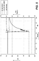
- the voltage of memory cell 200 depends upon the application of the current via the read word-line (RWL).
- Nodes A and B, shown in FIG. 2 may be viewed as terminals of a radio frequency transmission line.
- FIG. 2 shows a certain number of components of a memory cell 200 arranged in a certain manner, there could be more or fewer number of components arranged differently.
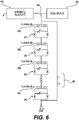
- each memory cell may have an LR shunt coupled in parallel to the memory cell.
- flux bias ⁇
- bit-line current e.g., bias current
- a flux pump 345 may be part of bit-line drivers 122 of FIG. 1 .
- a memory system including an array of memory cells arranged in rows and columns.
- the memory system includes: (1) a first set of word-lines, where each of the first set of the word-lines is coupled to a first plurality of memory cells in at least one row, and (2) a first set of bit-lines, where each of the first set of the bit-lines is coupled to a second plurality of memory cells in at least one column.
- any two components herein combined to achieve a particular functionality can be seen as “associated with” each other such that the desired functionality is achieved, irrespective of architectures or inter-medial components.
- any two components so associated can also be viewed as being “operably connected,” or “coupled,” to each other to achieve the desired functionality.
Landscapes
- Engineering & Computer Science (AREA)
- Computer Hardware Design (AREA)
- Semiconductor Memories (AREA)
- Superconductor Devices And Manufacturing Methods Thereof (AREA)
- Mram Or Spin Memory Techniques (AREA)
Claims (13)
- Speichersystem (100), umfassend:eine Matrix von Speicherzellen (102), die in Reihen und Spalten angeordnet sind;einen erster Satz von Wortlinien (114), wobei jeder des ersten Satzes der Wortlinien an eine erste Vielzahl von Speicherzellen (200) in mindestens einer Reihe gekoppelt ist;einen erster Satz von Bitlinien (124), wobei jeder des ersten Satzes der Bitlinien an eine zweite Vielzahl von Speicherzellen (200) in mindestens einer Spalte gekoppelt ist;wobei jede der ersten Vielzahl der Speicherzellen (200) und jede der zweiten Vielzahl der Speicherzellen (200) umfasst:mindestens ein Speicher-Speicherungselement (210), umfassend mindestens einen magnetischen Josephson-Übergang (220), selbst mindestens eine magnetische Sperrschicht umfassend, die konfiguriert ist, um als Reaktion auf ein Anlegen eines Wortlinienstroms über den mindestens einen des ersten Satzes der Wortlinien (114) an den mindestens einen magnetischen Josephson-Übergang entweder in einem ersten Zustand oder einem zweiten Zustand zu sein, wobei das mindestens eine Speicher-Speicherungselement weiter mindestens zwei Josephson-Übergänge (212, 214) und einen Induktor (222) umfasst, an den mindestens einen Josephson-Übergang gekoppelt, um eine einrastende Superconducting-Quantum-Interference-Device, SQUID, zu bilden; undmindestens einen Induktiv-Shunt (360, 370, 380, 390, 685, 695), der parallel an die mindestens eine Speicherzelle gekoppelt ist, wobei das Speichersystem weiter konfiguriert ist, um als Reaktion auf ein Anwenden eines Bitlinienstroms an den mindestens einen ersten Satz der Bitlinien (124) einen Lesevorgang auf dem mindestens einen Speicher-Speicherungselement (210) durchzuführen, wobei der mindestens eine Induktiv-Shunt konfiguriert ist, um nach dem Lesevorgang mindestens einen Abschnitt des Bitlinienstroms zu entfernen, der dem mindestens einen Speicher-Speicherungselement bereitgestellt wurde, ohne Entfernung einer Gesamtheit des Bitlinienstroms, der an den mindestens einen des ersten Satzes der Bitlinien während des Lesevorgangs angelegt wurde, zu erfordern, sodass der Abschnitt des Bitlinienstroms, der von dem mindestens einen Induktiv-Shunt entfernt wurde, ausreichend ist, um die einklinkende SQUID innerhalb der mindestens einen Speicherzelle abzuschalten.
- Speichersystem nach Anspruch 1, wobei der mindestens eine Induktiv-Shunt mindestens einen Widerstand umfasst, der mit mindestens einem Induktor in Reihe gekoppelt ist.
- Speichersystem nach Anspruch 1, wobei der mindestens eine Induktiv-Shunt konfiguriert ist, um den Abschnitt des Bitlinienstroms zu entfernen, der dem mindestens einen Speicher-Speicherungselement bereitgestellt wurde, ohne den mindestens einen des ersten Satzes der Bitlinien von dem mindestens einen Speicher-Speicherungselement zu entkoppeln.
- Speichersystem nach Anspruch 2, wobei der Wiederstand in dem mindestens einen Induktiv-Shunt konfiguriert ist, um den Bitlinienstrom nach Abschluss des Lesevorgangs zum mindestens einen des ersten Satzes der Bitlinien vor einem nächsten Lesevorgang umzuleiten.
- Speichersystem nach Anspruch 1, wobei das Speichersystem Komponenten basierend auf einer gegenseitigen Quantenlogik umfasst.
- Speichersystem nach Anspruch 1, wobei der erste Zustand einen ersten Magnetisierungszustand umfasst, der einer ersten Magnetisierungskonfiguration der mindestens einen magnetischen Sperrschicht entspricht, und der zweite Zustand einen zweiten Magnetisierungszustand umfasst, der einer zweiten Magnetisierungskonfiguration der mindestens einen magnetischen Sperrschicht entspricht, wobei die erste Konfigurierung der Magnetisierung sich von der zweiten Konfiguration der Magnetisierung unterscheidet.
- Verfahren zum Betreiben eines Speichersystems nach einem der Ansprüche 1-6, wobei das Verfahren umfasst:Durchführen eines ersten Lesevorgangs als Reaktion darauf, dass ein erster Bitlinienstrom an mindestens einen des ersten Satzes der Bitlinien angelegt wurde, die an das mindestens eine Speicher-Speicherungselement gekoppelt sind, und ein erster Wortlinienstrom an den mindestens einen des ersten Satzes von Wortlinien angelegt wurde, die an das mindestens eine Speicher-Speicherungselement gekoppelt sind; undVerwenden des Induktiv-Shunts (360, 370, 380, 685, 695), der parallel an die mindestens eine Speicherzelle gekoppelt ist, um mindestens einen Abschnitt des ersten Bitlinienstroms zu entfernen, der dem mindestens einen Speicher-Speicherungselement während des ersten Lesevorgangs bereitgestellt wurde, ohne Entfernung einer Gesamtheit des ersten Bitlinienstroms, der an den mindestens einen des ersten Satzes der Bitlinien während des Lesevorgangs angelegt wurde, zu erfordern, wobei das Entfernen des mindestens einen Abschnitts des ersten Bitlinienstroms, der dem mindestens einen Speicher-Speicherungselements bereitgestellt wurde, weiter Entfernen eines ausreichenden Stroms umfasst, um die einrastende Superconducting-Quantum-Interference-Device SQUID innerhalb der mindestens einen Speicherzelle abzuschalten.
- Verfahren nach Anspruch 7, wobei der Induktiv-Shunt mindestens einen Widerstand umfasst, der mit dem mindestens einen Induktor in Reihe geschaltet ist.
- Verfahren nach Anspruch 7, wobei während des ersten Lesevorgangs das mindestens eine Speicher-Speicherungselement in einem ersten Zustand oder einem zweiten Zustand ist und wobei der erste Zustand eine Spannungszustand ist und der zweite Zustand ein Nullzustand ist.
- Verfahren nach Anspruch 7, weiter umfassend Entfernen des mindestens einen Abschnitts des ersten Bitlinienstroms, der dem mindestens einen Speicher-Speicherungselement bereitgestellt wurde, ohne das mindestens eine Speicher-Speicherungselement von dem mindestens einen des ersten Satzes der Bitlinien zu entkoppeln.
- Verfahren nach Anspruch 7, weiter umfassend, nach einer vorbestimmten Anzahl von Taktzyklen, Durchführen eines zweiten Lesevorgangs als Reaktion auf einen zweiten Bitlinienstrom, der an den mindestens einen des ersten Satzes der Bitlinien angelegt wurde.
- Verfahren nach Anspruch 11, wobei das Speichersystem Komponenten basierend auf gegenseitiger Quantenlogik umfasst und wobei die Taktzyklen einem sinusförmigem Takt entsprechen.
- Speichersystem nach Anspruch 1,
wobei die mindestens eine magnetische Sperrschicht des mindestens einen magnetischen Josephson-Übergangs konfiguriert ist, um als Reaktion auf ein Anlegen eines Wortlinienstroms über mindestens einen des ersten Satzes der Wortlinien an den mindestens einen magnetischen Josephson-Übergang entweder in einem ersten Magnetisierungszustand oder einem zweiten Magnetisierungszustand zu sein, und
wobei das mindestens eine Speicher-Speicherungselement mindestens N Speicher-Speicherungselementen ist, wobei N eine positive ganze Zahl ist.
Applications Claiming Priority (2)
| Application Number | Priority Date | Filing Date | Title |
|---|---|---|---|
| US14/935,862 US9443576B1 (en) | 2015-11-09 | 2015-11-09 | Josephson magnetic random access memory with an inductive-shunt |
| PCT/US2016/060209 WO2017083154A1 (en) | 2015-11-09 | 2016-11-03 | Josephson magnetic random access memory with an inductive-shunt |
Publications (2)
| Publication Number | Publication Date |
|---|---|
| EP3374995A1 EP3374995A1 (de) | 2018-09-19 |
| EP3374995B1 true EP3374995B1 (de) | 2019-08-14 |
Family
ID=56881411
Family Applications (1)
| Application Number | Title | Priority Date | Filing Date |
|---|---|---|---|
| EP16795516.0A Active EP3374995B1 (de) | 2015-11-09 | 2016-11-03 | Josephson-magnet-direktzugriffsspeicher mit einem induktiven shunt |
Country Status (4)
| Country | Link |
|---|---|
| US (1) | US9443576B1 (de) |
| EP (1) | EP3374995B1 (de) |
| CN (1) | CN108352180B (de) |
| WO (1) | WO2017083154A1 (de) |
Families Citing this family (47)
| Publication number | Priority date | Publication date | Assignee | Title |
|---|---|---|---|---|
| US8571614B1 (en) | 2009-10-12 | 2013-10-29 | Hypres, Inc. | Low-power biasing networks for superconducting integrated circuits |
| US10222416B1 (en) | 2015-04-14 | 2019-03-05 | Hypres, Inc. | System and method for array diagnostics in superconducting integrated circuit |
| US9922719B2 (en) * | 2015-06-07 | 2018-03-20 | Sandisk Technologies Llc | Multi-VT sensing method by varying bit line voltage |
| US9779803B1 (en) * | 2017-03-01 | 2017-10-03 | Northrop Grumman Systems Corporation | Memory circuit with write-bypass portion |
| WO2019160572A2 (en) | 2017-05-16 | 2019-08-22 | PsiQuantum Corp. | Gated superconducting photon detector |
| WO2019160573A2 (en) | 2017-05-16 | 2019-08-22 | PsiQuantum Corp. | Superconducting signal amplifier |
| US10488469B2 (en) * | 2017-06-05 | 2019-11-26 | The Regents Of The University Of California | Magnetic flux control in superconducting devices |
| US10262727B2 (en) | 2017-07-10 | 2019-04-16 | Northrop Grumman Systems Corporation | Gradiometric flux qubit system |
| US10566516B2 (en) | 2017-07-28 | 2020-02-18 | PsiQuantum Corp. | Photodetector with superconductor nanowire transistor based on interlayer heat transfer |
| US10361703B2 (en) | 2017-10-05 | 2019-07-23 | PsiQuantum Corp. | Superconducting logic circuits |
| US10461445B2 (en) | 2017-11-13 | 2019-10-29 | PsiQuantum Corp. | Methods and devices for impedance multiplication |
| US10417136B2 (en) * | 2017-12-21 | 2019-09-17 | Northrop Grumman Systems Corporation | Write-through detection for a memory circuit with an analog bypass portion |
| WO2019157077A1 (en) | 2018-02-06 | 2019-08-15 | PsiQuantum Corp. | Superconducting photon detector |
| WO2019160869A1 (en) | 2018-02-14 | 2019-08-22 | PsiQuantum Corp. | Superconducting logic components |
| US10204677B1 (en) * | 2018-03-16 | 2019-02-12 | Microsoft Technology Licensing, Llc | Superconducting memory system with stacked drivers and differential transformers |
| WO2019213147A1 (en) | 2018-05-01 | 2019-11-07 | PsiQuantum Corp. | Photon number resolving superconducting detector |
| US10541024B2 (en) | 2018-05-25 | 2020-01-21 | Microsoft Technology Licensing, Llc | Memory system with signals on read lines not phase-aligned with Josephson transmission line (JTL) elements included in the write lines |
| US10546621B2 (en) * | 2018-06-20 | 2020-01-28 | Microsoft Technology Licensing, Llc | Magnetic josephson junction driven flux-biased superconductor memory cell and methods |
| US10447278B1 (en) | 2018-07-17 | 2019-10-15 | Northrop Grumman Systems Corporation | JTL-based superconducting logic arrays and FPGAs |
| US10984857B2 (en) | 2018-08-16 | 2021-04-20 | PsiQuantum Corp. | Superconductive memory cells and devices |
| US10573800B1 (en) | 2018-08-21 | 2020-02-25 | PsiQuantum Corp. | Superconductor-to-insulator devices |
| US10818346B2 (en) * | 2018-09-17 | 2020-10-27 | Northrop Grumman Systems Corporation | Quantizing loop memory cell system |
| US11101215B2 (en) | 2018-09-19 | 2021-08-24 | PsiQuantum Corp. | Tapered connectors for superconductor circuits |
| US11719653B1 (en) | 2018-09-21 | 2023-08-08 | PsiQuantum Corp. | Methods and systems for manufacturing superconductor devices |
| CN109524035B (zh) * | 2018-10-10 | 2020-06-09 | 中国科学院上海微系统与信息技术研究所 | 存储单元、嵌入式存储器及其读写方法 |
| US11121302B2 (en) | 2018-10-11 | 2021-09-14 | SeeQC, Inc. | System and method for superconducting multi-chip module |
| US10734568B2 (en) * | 2018-10-25 | 2020-08-04 | Northrop Grumman Systems Corporation | Milliohm resistor for RQL circuits |
| US10944403B2 (en) | 2018-10-27 | 2021-03-09 | PsiQuantum Corp. | Superconducting field-programmable gate array |
| US10587245B1 (en) * | 2018-11-13 | 2020-03-10 | Northrop Grumman Systems Corporation | Superconducting transmission line driver system |
| US11289590B1 (en) | 2019-01-30 | 2022-03-29 | PsiQuantum Corp. | Thermal diode switch |
| US10910544B2 (en) * | 2019-02-26 | 2021-02-02 | Microsoft Technology Licensing, Llc | Using a magnetic Josephson junction device as a pi inverter |
| JP7344499B2 (ja) * | 2019-03-01 | 2023-09-14 | 国立大学法人横浜国立大学 | 光子検出装置 |
| US11569816B1 (en) | 2019-04-10 | 2023-01-31 | PsiQuantum Corp. | Superconducting switch |
| US11009387B2 (en) | 2019-04-16 | 2021-05-18 | PsiQuantum Corp. | Superconducting nanowire single photon detector and method of fabrication thereof |
| US11380731B1 (en) | 2019-09-26 | 2022-07-05 | PsiQuantum Corp. | Superconducting device with asymmetric impedance |
| US11585695B1 (en) | 2019-10-21 | 2023-02-21 | PsiQuantum Corp. | Self-triaging photon detector |
| CN110739010B (zh) * | 2019-10-21 | 2021-05-11 | 中国科学院上海微系统与信息技术研究所 | 低温存储单元及存储器件 |
| US11994426B1 (en) | 2019-11-13 | 2024-05-28 | PsiQuantum Corp. | Scalable photon number resolving photon detector |
| US11056634B1 (en) * | 2019-12-16 | 2021-07-06 | Microsoft Technology Licensing, Llc | Josephson magnetic memory with a semiconductor-based magnetic spin valve |
| US11024791B1 (en) | 2020-01-27 | 2021-06-01 | Northrop Grumman Systems Corporation | Magnetically stabilized magnetic Josephson junction memory cell |
| US11545288B2 (en) | 2020-04-15 | 2023-01-03 | Northrop Grumman Systems Corporation | Superconducting current control system |
| US11269779B2 (en) * | 2020-05-27 | 2022-03-08 | Microsoft Technology Licensing, Llc | Memory system with a predictable read latency from media with a long write latency |
| CN111724836B (zh) * | 2020-06-03 | 2022-06-07 | 中国科学院上海微系统与信息技术研究所 | 一种超导磁通存储单元及其读写方法 |
| US11282557B2 (en) * | 2020-06-22 | 2022-03-22 | Micron Technology, Inc. | Magnetic cache for a memory device |
| US11757467B2 (en) | 2021-08-13 | 2023-09-12 | Northrop Grumman Systems Corporation | Circuits for converting SFQ-based RZ and NRZ signaling to bilevel voltage NRZ signaling |
| US12597925B2 (en) | 2022-12-08 | 2026-04-07 | Northrop Grumman Systems Corporation | Superconducting current control system |
| US12395140B2 (en) | 2023-07-27 | 2025-08-19 | Northrop Grumman Systems Corporation | Non-return to zero (NRZ) amplifier system |
Family Cites Families (16)
| Publication number | Priority date | Publication date | Assignee | Title |
|---|---|---|---|---|
| US3164808A (en) * | 1960-05-02 | 1965-01-05 | Thompson Ramo Wooldridge Inc | Superconductive information handling arrangement |
| US4151605A (en) | 1977-11-22 | 1979-04-24 | International Business Machines Corporation | Superconducting memory array configurations which avoid spurious half-select condition in unselected cells of the array |
| US4509146A (en) * | 1982-12-02 | 1985-04-02 | Sperry Corporation | High density Josephson junction memory circuit |
| JPH03276493A (ja) * | 1990-03-26 | 1991-12-06 | Agency Of Ind Science & Technol | ジョセフソン・メモリ回路 |
| US5610857A (en) * | 1996-03-25 | 1997-03-11 | Tektronix, Inc. | Memory element with multibit storage |
| US5872731A (en) | 1997-10-10 | 1999-02-16 | Trw Inc. | Multi-state Josephson memory |
| US6154044A (en) | 1998-11-20 | 2000-11-28 | Trw Inc. | Superconductive logic gate and random access memory |
| US6242939B1 (en) | 1999-03-05 | 2001-06-05 | Nec Corporation | Superconducting circuit having superconductive circuit device of voltage-type logic and superconductive circuit device of fluxoid-type logic device selectively used therein |
| US6960929B2 (en) * | 2001-07-23 | 2005-11-01 | Bedard Fernand D | Superconductive crossbar switch |
| US6809949B2 (en) * | 2002-05-06 | 2004-10-26 | Symetrix Corporation | Ferroelectric memory |
| US8208288B2 (en) | 2008-03-27 | 2012-06-26 | International Business Machines Corporation | Hybrid superconducting-magnetic memory cell and array |
| US8270209B2 (en) | 2010-04-30 | 2012-09-18 | Northrop Grumman Systems Corporation | Josephson magnetic random access memory system and method |
| US8971977B2 (en) | 2011-01-17 | 2015-03-03 | Hypres, Inc. | Superconducting devices with ferromagnetic barrier junctions |
| US9013916B2 (en) | 2012-05-31 | 2015-04-21 | Northrop Grumman Systems Corporation | Josephson magnetic memory cell system |
| WO2014197095A2 (en) | 2013-03-14 | 2014-12-11 | Andrew Bleloch | Flux latching superconducting memory |
| US9208861B2 (en) | 2013-10-01 | 2015-12-08 | Northrop Grumman Systems Corporation | Phase hysteretic magnetic Josephson junction memory cell |
-
2015
- 2015-11-09 US US14/935,862 patent/US9443576B1/en active Active
-
2016
- 2016-11-03 CN CN201680065079.3A patent/CN108352180B/zh active Active
- 2016-11-03 WO PCT/US2016/060209 patent/WO2017083154A1/en not_active Ceased
- 2016-11-03 EP EP16795516.0A patent/EP3374995B1/de active Active
Non-Patent Citations (1)
| Title |
|---|
| None * |
Also Published As
| Publication number | Publication date |
|---|---|
| EP3374995A1 (de) | 2018-09-19 |
| WO2017083154A1 (en) | 2017-05-18 |
| US9443576B1 (en) | 2016-09-13 |
| CN108352180A (zh) | 2018-07-31 |
| CN108352180B (zh) | 2021-09-10 |
Similar Documents
| Publication | Publication Date | Title |
|---|---|---|
| US9443576B1 (en) | Josephson magnetic random access memory with an inductive-shunt | |
| US10923646B2 (en) | Superconducting switch having a persistent and a non-persistent state | |
| EP3811362B1 (de) | Magnetische josephson-übergangs-getriebene flussvorbelastete supraleiter-speicherzelle und verfahren | |
| US9972380B2 (en) | Memory cell having a magnetic Josephson junction device with a doped magnetic layer | |
| US11717475B1 (en) | System and method for cryogenic hybrid technology computing and memory | |
| EP3766069B1 (de) | Supraleitendes speichersystem mit gestapelten treibern und differentialtransformatoren | |
| US9552862B2 (en) | Magnetic ram array architecture | |
| US10650884B2 (en) | Superconducting memory with josephson phase-based torque | |
| EP3803874B1 (de) | Strombasierte supraleitende speicherzelle und verfahren | |
| CN113474839B (zh) | 使用磁约瑟夫森结器件作为π反相器 |
Legal Events
| Date | Code | Title | Description |
|---|---|---|---|
| STAA | Information on the status of an ep patent application or granted ep patent |
Free format text: STATUS: UNKNOWN |
|
| STAA | Information on the status of an ep patent application or granted ep patent |
Free format text: STATUS: THE INTERNATIONAL PUBLICATION HAS BEEN MADE |
|
| PUAI | Public reference made under article 153(3) epc to a published international application that has entered the european phase |
Free format text: ORIGINAL CODE: 0009012 |
|
| STAA | Information on the status of an ep patent application or granted ep patent |
Free format text: STATUS: REQUEST FOR EXAMINATION WAS MADE |
|
| 17P | Request for examination filed |
Effective date: 20180419 |
|
| AK | Designated contracting states |
Kind code of ref document: A1 Designated state(s): AL AT BE BG CH CY CZ DE DK EE ES FI FR GB GR HR HU IE IS IT LI LT LU LV MC MK MT NL NO PL PT RO RS SE SI SK SM TR |
|
| AX | Request for extension of the european patent |
Extension state: BA ME |
|
| DAV | Request for validation of the european patent (deleted) | ||
| DAX | Request for extension of the european patent (deleted) | ||
| GRAP | Despatch of communication of intention to grant a patent |
Free format text: ORIGINAL CODE: EPIDOSNIGR1 |
|
| STAA | Information on the status of an ep patent application or granted ep patent |
Free format text: STATUS: GRANT OF PATENT IS INTENDED |
|
| INTG | Intention to grant announced |
Effective date: 20190307 |
|
| GRAS | Grant fee paid |
Free format text: ORIGINAL CODE: EPIDOSNIGR3 |
|
| GRAA | (expected) grant |
Free format text: ORIGINAL CODE: 0009210 |
|
| STAA | Information on the status of an ep patent application or granted ep patent |
Free format text: STATUS: THE PATENT HAS BEEN GRANTED |
|
| AK | Designated contracting states |
Kind code of ref document: B1 Designated state(s): AL AT BE BG CH CY CZ DE DK EE ES FI FR GB GR HR HU IE IS IT LI LT LU LV MC MK MT NL NO PL PT RO RS SE SI SK SM TR |
|
| REG | Reference to a national code |
Ref country code: GB Ref legal event code: FG4D |
|
| REG | Reference to a national code |
Ref country code: CH Ref legal event code: EP Ref country code: AT Ref legal event code: REF Ref document number: 1167982 Country of ref document: AT Kind code of ref document: T Effective date: 20190815 |
|
| REG | Reference to a national code |
Ref country code: IE Ref legal event code: FG4D |
|
| REG | Reference to a national code |
Ref country code: DE Ref legal event code: R096 Ref document number: 602016018747 Country of ref document: DE |
|
| REG | Reference to a national code |
Ref country code: NL Ref legal event code: FP |
|
| REG | Reference to a national code |
Ref country code: DE Ref legal event code: R082 Ref document number: 602016018747 Country of ref document: DE |
|
| REG | Reference to a national code |
Ref country code: LT Ref legal event code: MG4D |
|
| PG25 | Lapsed in a contracting state [announced via postgrant information from national office to epo] |
Ref country code: PT Free format text: LAPSE BECAUSE OF FAILURE TO SUBMIT A TRANSLATION OF THE DESCRIPTION OR TO PAY THE FEE WITHIN THE PRESCRIBED TIME-LIMIT Effective date: 20191216 Ref country code: NO Free format text: LAPSE BECAUSE OF FAILURE TO SUBMIT A TRANSLATION OF THE DESCRIPTION OR TO PAY THE FEE WITHIN THE PRESCRIBED TIME-LIMIT Effective date: 20191114 Ref country code: SE Free format text: LAPSE BECAUSE OF FAILURE TO SUBMIT A TRANSLATION OF THE DESCRIPTION OR TO PAY THE FEE WITHIN THE PRESCRIBED TIME-LIMIT Effective date: 20190814 Ref country code: FI Free format text: LAPSE BECAUSE OF FAILURE TO SUBMIT A TRANSLATION OF THE DESCRIPTION OR TO PAY THE FEE WITHIN THE PRESCRIBED TIME-LIMIT Effective date: 20190814 Ref country code: HR Free format text: LAPSE BECAUSE OF FAILURE TO SUBMIT A TRANSLATION OF THE DESCRIPTION OR TO PAY THE FEE WITHIN THE PRESCRIBED TIME-LIMIT Effective date: 20190814 Ref country code: LT Free format text: LAPSE BECAUSE OF FAILURE TO SUBMIT A TRANSLATION OF THE DESCRIPTION OR TO PAY THE FEE WITHIN THE PRESCRIBED TIME-LIMIT Effective date: 20190814 Ref country code: BG Free format text: LAPSE BECAUSE OF FAILURE TO SUBMIT A TRANSLATION OF THE DESCRIPTION OR TO PAY THE FEE WITHIN THE PRESCRIBED TIME-LIMIT Effective date: 20191114 |
|
| REG | Reference to a national code |
Ref country code: AT Ref legal event code: MK05 Ref document number: 1167982 Country of ref document: AT Kind code of ref document: T Effective date: 20190814 |
|
| PG25 | Lapsed in a contracting state [announced via postgrant information from national office to epo] |
Ref country code: AL Free format text: LAPSE BECAUSE OF FAILURE TO SUBMIT A TRANSLATION OF THE DESCRIPTION OR TO PAY THE FEE WITHIN THE PRESCRIBED TIME-LIMIT Effective date: 20190814 Ref country code: GR Free format text: LAPSE BECAUSE OF FAILURE TO SUBMIT A TRANSLATION OF THE DESCRIPTION OR TO PAY THE FEE WITHIN THE PRESCRIBED TIME-LIMIT Effective date: 20191115 Ref country code: ES Free format text: LAPSE BECAUSE OF FAILURE TO SUBMIT A TRANSLATION OF THE DESCRIPTION OR TO PAY THE FEE WITHIN THE PRESCRIBED TIME-LIMIT Effective date: 20190814 Ref country code: LV Free format text: LAPSE BECAUSE OF FAILURE TO SUBMIT A TRANSLATION OF THE DESCRIPTION OR TO PAY THE FEE WITHIN THE PRESCRIBED TIME-LIMIT Effective date: 20190814 Ref country code: RS Free format text: LAPSE BECAUSE OF FAILURE TO SUBMIT A TRANSLATION OF THE DESCRIPTION OR TO PAY THE FEE WITHIN THE PRESCRIBED TIME-LIMIT Effective date: 20190814 Ref country code: IS Free format text: LAPSE BECAUSE OF FAILURE TO SUBMIT A TRANSLATION OF THE DESCRIPTION OR TO PAY THE FEE WITHIN THE PRESCRIBED TIME-LIMIT Effective date: 20191214 |
|
| PG25 | Lapsed in a contracting state [announced via postgrant information from national office to epo] |
Ref country code: TR Free format text: LAPSE BECAUSE OF FAILURE TO SUBMIT A TRANSLATION OF THE DESCRIPTION OR TO PAY THE FEE WITHIN THE PRESCRIBED TIME-LIMIT Effective date: 20190814 |
|
| PG25 | Lapsed in a contracting state [announced via postgrant information from national office to epo] |
Ref country code: RO Free format text: LAPSE BECAUSE OF FAILURE TO SUBMIT A TRANSLATION OF THE DESCRIPTION OR TO PAY THE FEE WITHIN THE PRESCRIBED TIME-LIMIT Effective date: 20190814 Ref country code: PL Free format text: LAPSE BECAUSE OF FAILURE TO SUBMIT A TRANSLATION OF THE DESCRIPTION OR TO PAY THE FEE WITHIN THE PRESCRIBED TIME-LIMIT Effective date: 20190814 Ref country code: EE Free format text: LAPSE BECAUSE OF FAILURE TO SUBMIT A TRANSLATION OF THE DESCRIPTION OR TO PAY THE FEE WITHIN THE PRESCRIBED TIME-LIMIT Effective date: 20190814 Ref country code: AT Free format text: LAPSE BECAUSE OF FAILURE TO SUBMIT A TRANSLATION OF THE DESCRIPTION OR TO PAY THE FEE WITHIN THE PRESCRIBED TIME-LIMIT Effective date: 20190814 Ref country code: DK Free format text: LAPSE BECAUSE OF FAILURE TO SUBMIT A TRANSLATION OF THE DESCRIPTION OR TO PAY THE FEE WITHIN THE PRESCRIBED TIME-LIMIT Effective date: 20190814 Ref country code: IT Free format text: LAPSE BECAUSE OF FAILURE TO SUBMIT A TRANSLATION OF THE DESCRIPTION OR TO PAY THE FEE WITHIN THE PRESCRIBED TIME-LIMIT Effective date: 20190814 |
|
| PG25 | Lapsed in a contracting state [announced via postgrant information from national office to epo] |
Ref country code: IS Free format text: LAPSE BECAUSE OF FAILURE TO SUBMIT A TRANSLATION OF THE DESCRIPTION OR TO PAY THE FEE WITHIN THE PRESCRIBED TIME-LIMIT Effective date: 20200224 Ref country code: CZ Free format text: LAPSE BECAUSE OF FAILURE TO SUBMIT A TRANSLATION OF THE DESCRIPTION OR TO PAY THE FEE WITHIN THE PRESCRIBED TIME-LIMIT Effective date: 20190814 Ref country code: SM Free format text: LAPSE BECAUSE OF FAILURE TO SUBMIT A TRANSLATION OF THE DESCRIPTION OR TO PAY THE FEE WITHIN THE PRESCRIBED TIME-LIMIT Effective date: 20190814 Ref country code: SK Free format text: LAPSE BECAUSE OF FAILURE TO SUBMIT A TRANSLATION OF THE DESCRIPTION OR TO PAY THE FEE WITHIN THE PRESCRIBED TIME-LIMIT Effective date: 20190814 |
|
| REG | Reference to a national code |
Ref country code: DE Ref legal event code: R097 Ref document number: 602016018747 Country of ref document: DE |
|
| REG | Reference to a national code |
Ref country code: CH Ref legal event code: PL |
|
| PLBE | No opposition filed within time limit |
Free format text: ORIGINAL CODE: 0009261 |
|
| STAA | Information on the status of an ep patent application or granted ep patent |
Free format text: STATUS: NO OPPOSITION FILED WITHIN TIME LIMIT |
|
| PG2D | Information on lapse in contracting state deleted |
Ref country code: IS |
|
| PG25 | Lapsed in a contracting state [announced via postgrant information from national office to epo] |
Ref country code: MC Free format text: LAPSE BECAUSE OF FAILURE TO SUBMIT A TRANSLATION OF THE DESCRIPTION OR TO PAY THE FEE WITHIN THE PRESCRIBED TIME-LIMIT Effective date: 20190814 Ref country code: LI Free format text: LAPSE BECAUSE OF NON-PAYMENT OF DUE FEES Effective date: 20191130 Ref country code: CH Free format text: LAPSE BECAUSE OF NON-PAYMENT OF DUE FEES Effective date: 20191130 Ref country code: LU Free format text: LAPSE BECAUSE OF NON-PAYMENT OF DUE FEES Effective date: 20191103 |
|
| 26N | No opposition filed |
Effective date: 20200603 |
|
| REG | Reference to a national code |
Ref country code: BE Ref legal event code: MM Effective date: 20191130 |
|
| PG25 | Lapsed in a contracting state [announced via postgrant information from national office to epo] |
Ref country code: SI Free format text: LAPSE BECAUSE OF FAILURE TO SUBMIT A TRANSLATION OF THE DESCRIPTION OR TO PAY THE FEE WITHIN THE PRESCRIBED TIME-LIMIT Effective date: 20190814 |
|
| PG25 | Lapsed in a contracting state [announced via postgrant information from national office to epo] |
Ref country code: IE Free format text: LAPSE BECAUSE OF NON-PAYMENT OF DUE FEES Effective date: 20191103 |
|
| PG25 | Lapsed in a contracting state [announced via postgrant information from national office to epo] |
Ref country code: BE Free format text: LAPSE BECAUSE OF NON-PAYMENT OF DUE FEES Effective date: 20191130 |
|
| PG25 | Lapsed in a contracting state [announced via postgrant information from national office to epo] |
Ref country code: CY Free format text: LAPSE BECAUSE OF FAILURE TO SUBMIT A TRANSLATION OF THE DESCRIPTION OR TO PAY THE FEE WITHIN THE PRESCRIBED TIME-LIMIT Effective date: 20190814 |
|
| PG25 | Lapsed in a contracting state [announced via postgrant information from national office to epo] |
Ref country code: MT Free format text: LAPSE BECAUSE OF FAILURE TO SUBMIT A TRANSLATION OF THE DESCRIPTION OR TO PAY THE FEE WITHIN THE PRESCRIBED TIME-LIMIT Effective date: 20190814 Ref country code: HU Free format text: LAPSE BECAUSE OF FAILURE TO SUBMIT A TRANSLATION OF THE DESCRIPTION OR TO PAY THE FEE WITHIN THE PRESCRIBED TIME-LIMIT; INVALID AB INITIO Effective date: 20161103 |
|
| PG25 | Lapsed in a contracting state [announced via postgrant information from national office to epo] |
Ref country code: MK Free format text: LAPSE BECAUSE OF FAILURE TO SUBMIT A TRANSLATION OF THE DESCRIPTION OR TO PAY THE FEE WITHIN THE PRESCRIBED TIME-LIMIT Effective date: 20190814 |
|
| P01 | Opt-out of the competence of the unified patent court (upc) registered |
Effective date: 20230429 |
|
| PGFP | Annual fee paid to national office [announced via postgrant information from national office to epo] |
Ref country code: NL Payment date: 20251022 Year of fee payment: 10 |
|
| PGFP | Annual fee paid to national office [announced via postgrant information from national office to epo] |
Ref country code: DE Payment date: 20251022 Year of fee payment: 10 |
|
| PGFP | Annual fee paid to national office [announced via postgrant information from national office to epo] |
Ref country code: GB Payment date: 20251023 Year of fee payment: 10 |
|
| PGFP | Annual fee paid to national office [announced via postgrant information from national office to epo] |
Ref country code: FR Payment date: 20251022 Year of fee payment: 10 |