US12061212B2 - Spring contact and socket having spring contact embedded therein - Google Patents
Spring contact and socket having spring contact embedded therein Download PDFInfo
- Publication number
- US12061212B2 US12061212B2 US17/609,912 US201917609912A US12061212B2 US 12061212 B2 US12061212 B2 US 12061212B2 US 201917609912 A US201917609912 A US 201917609912A US 12061212 B2 US12061212 B2 US 12061212B2
- Authority
- US
- United States
- Prior art keywords
- contact
- contact pin
- spring
- socket
- body portion
- Prior art date
- Legal status (The legal status is an assumption and is not a legal conclusion. Google has not performed a legal analysis and makes no representation as to the accuracy of the status listed.)
- Active, expires
Links
Images


Classifications
-
- G—PHYSICS
- G01—MEASURING; TESTING
- G01R—MEASURING ELECTRIC VARIABLES; MEASURING MAGNETIC VARIABLES
- G01R1/00—Details of instruments or arrangements of the types included in groups G01R5/00 - G01R13/00 and G01R31/00
- G01R1/02—General constructional details
- G01R1/04—Housings; Supporting members; Arrangements of terminals
- G01R1/0408—Test fixtures or contact fields; Connectors or connecting adaptors; Test clips; Test sockets
- G01R1/0433—Sockets for IC's or transistors
- G01R1/0441—Details
- G01R1/0466—Details concerning contact pieces or mechanical details, e.g. hinges or cams; Shielding
-
- G—PHYSICS
- G01—MEASURING; TESTING
- G01R—MEASURING ELECTRIC VARIABLES; MEASURING MAGNETIC VARIABLES
- G01R1/00—Details of instruments or arrangements of the types included in groups G01R5/00 - G01R13/00 and G01R31/00
- G01R1/02—General constructional details
- G01R1/04—Housings; Supporting members; Arrangements of terminals
- G01R1/0408—Test fixtures or contact fields; Connectors or connecting adaptors; Test clips; Test sockets
- G01R1/0433—Sockets for IC's or transistors
- G01R1/0483—Sockets for un-leaded IC's having matrix type contact fields, e.g. BGA or PGA devices; Sockets for unpackaged, naked chips
-
- G—PHYSICS
- G01—MEASURING; TESTING
- G01R—MEASURING ELECTRIC VARIABLES; MEASURING MAGNETIC VARIABLES
- G01R1/00—Details of instruments or arrangements of the types included in groups G01R5/00 - G01R13/00 and G01R31/00
- G01R1/02—General constructional details
- G01R1/06—Measuring leads; Measuring probes
- G01R1/067—Measuring probes
- G01R1/06711—Probe needles; Cantilever beams; "Bump" contacts; Replaceable probe pins
- G01R1/06716—Elastic
- G01R1/06722—Spring-loaded
-
- G—PHYSICS
- G01—MEASURING; TESTING
- G01R—MEASURING ELECTRIC VARIABLES; MEASURING MAGNETIC VARIABLES
- G01R1/00—Details of instruments or arrangements of the types included in groups G01R5/00 - G01R13/00 and G01R31/00
- G01R1/02—General constructional details
- G01R1/06—Measuring leads; Measuring probes
- G01R1/067—Measuring probes
- G01R1/073—Multiple probes
- G01R1/07307—Multiple probes with individual probe elements, e.g. needles, cantilever beams or bump contacts, fixed in relation to each other, e.g. bed of nails fixture or probe card
- G01R1/07314—Multiple probes with individual probe elements, e.g. needles, cantilever beams or bump contacts, fixed in relation to each other, e.g. bed of nails fixture or probe card the body of the probe being perpendicular to test object, e.g. bed of nails or probe with bump contacts on a rigid support
-
- G—PHYSICS
- G01—MEASURING; TESTING
- G01R—MEASURING ELECTRIC VARIABLES; MEASURING MAGNETIC VARIABLES
- G01R31/00—Arrangements for testing electric properties; Arrangements for locating electric faults; Arrangements for electrical testing characterised by what is being tested not provided for elsewhere
- G01R31/28—Testing of electronic circuits, e.g. by signal tracer
- G01R31/2851—Testing of integrated circuits [IC]
- G01R31/2886—Features relating to contacting the IC under test, e.g. probe heads; chucks
Definitions
- the present disclosure relates generally to a spring contact and a socket having spring contact embedded therein. More particularly, the present disclosure relates to a spring contact that electrically connects each of a plurality of leads of an integrated circuit (IC) to an associated one of a plurality of pads of a printed circuit board (PCB) for the test of the performance of the IC or electrically connects each of leads of an IC such as a central processing unit (CPU) to a PCB of an electronic appliance such as a personal computer (PC) or a mobile phone, and relates to a socket with the same.
- IC integrated circuit
- PCB printed circuit board
- spring contacts serve to electrically connect a PCB with leads of an IC, and are essential components of a socket for testing ICs.
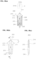
- FIGS. 1 to 3 illustrate a spring contact in the related art
- FIGS. 4 and 5 illustrate a socket with a spring contact.
- FIGS. 1 ( a ) and 1 ( b ) are respectively a perspective view and an exploded perspective view illustrating a spring contact in the related art.
- the spring contact includes an upper contact pin 10 , a lower contact pin 20 assembled to the upper contact pin 10 in such a manner that the upper and lower contact pins cross each other in longitudinal directions thereof, and a spring 30 fitted over the upper and lower contact pins 10 and 20 at a position therebetween to elastically support the upper and lower contact pins 10 and 20 .
- FIGS. 2 ( a ) and 2 ( b ) are respectively a plan view illustrating the upper contact pin 10 in the related art and a sectional view taken along line A-A.
- the upper contact pin 10 includes a contact portion 11 protruding from an upper end of the upper contact pin, a pair of fixing protrusions 12 protruding from left and right sides of the upper contact pin 10 , a body portion 13 including a flow groove 13 a recessed in a longitudinal direction thereof, a pair of elastic portions 14 extending symmetrically from the body portion 13 , and a locking protrusion 15 provided at an end of each of the elastic portions 14 .
- the lower contact pin 20 has the same shape as the upper contact pin 10 .
- FIGS. 3 ( a ) and 3 ( b ) are respective views illustrating an operation example of the spring contact in the related art, in which the left and right views of FIG. 3 ( a ) illustrate respectively before and after compression of the spring 30 , and the left and right views of FIG. 3 ( b ) illustrate in plan view the position between the upper and lower contact pins 10 and 20 before and after the compression of the spring 30 .
- the upper contact pin 10 and the lower contact pin 20 are assembled together with the spring 30 fitted thereover in such a manner that the elastic portions 14 and 24 are perpendicular to each other in the longitudinal directions of the contact pins.
- the respective locking protrusions 15 of the upper contact pin 10 are inserted into a flow groove 23 a of the lower contact pin 20 and locking protrusions 25 of the lower contact pin 20 are inserted into the flow groove 13 a of the upper contact pin 10 . Therefore, when an external force acts in a longitudinal direction of the spring contact, the locking protrusions 15 and 25 are moved along the flow grooves 13 a and 23 a while the upper contact pin 10 and the lower contact pin 20 are compressed by a predetermined length S.
- the maximum displacement (Smax) between the upper contact pin 10 and the lower contact pin 20 is determined by the position (left view) where the locking protrusions 15 and 25 of the upper and lower contact pins 10 and 20 are supported at the ends of the opposing flow grooves 13 a and 23 a before the spring 30 is compressed, and the position (right view) where end portions 13 b and 23 b of the bodies 13 and 23 of the upper and lower contact pins 10 and 20 come into contact with each other in a compressed state of the spring 30 .
- FIG. 4 is a plan view illustrating the socket in the related art
- FIG. 5 is a sectional view taken along line B-B of FIG. 4 .
- the socket in the related art includes an upper plate 40 and a lower plate 50 assembled to the upper plate 40 by fitting, with a spring contact 1 fixed between the upper plate 40 and the lower plate 50 .
- the upper plate 40 and the lower plate 50 respectively include receiving holes 41 and 51 to which the spring contact 1 is fixed.
- the spring contact 1 is located in the receiving holes 41 and 51 between the upper and lower plates 40 and 50 such that upper and lower ends thereof protrude outside the receiving holes 41 and 51 , and serves to electrically connect a lead of an IC and a pad of a PCB to each other.
- the socket in the related art is manufactured in such a manner that the upper and lower plates 40 and 50 are made of synthetic resin.
- a flange portion 42 in which the first receiving hole 41 is formed is provided by protruding from the upper plate 40 by a predetermined height such that the spring contact 1 of a predetermined height is received therein.
- a high processing cost is required. Also, there is a limitation in manufacturing a plate having a thickness of equal to or less than 1.0 mm, and, due thereto, it is difficult to manufacture a test socket for high speed use for processing a high-speed signal of equal to or greater than 40 GHz.
- the rubber-type socket may include a stretchable insulating body having an insulating silicone powder solidified therein, and a conductive silicone portion formed in the insulating body by vertically passing therethrough at a position corresponding to a lead of an IC.
- the rubber-type socket may be manufactured in such a manner that when a silicone mixture containing insulating silicone and conductive powder in a predetermined ratio is placed into a mold and a strong magnetic field is formed at a position where the conductive silicone portion is to be formed, the conductive powder of the silicon mixture is collected at the position where the magnetic field is formed and finally a molten silicone mixture is solidified to form an array of conductive silicone portions in the insulating body.
- the rubber-type socket is disadvantageous in that the speed of elastic response may be slower than that of a pin-type contact (spring contact) and the elasticity may be lost in the course of a repeated test process, which may result in a short service life and increased costs due to frequent replacement.
- the elastic repulsive force may become zero or remarkably low during continuous compression test for a long period of time (more than one week), and thus a short circuit may occur, which may make it difficult to use the rubber-type socket for long term testing.
- the rubber-type socket is problematic in that the elastic characteristics may be affected greatly by the temperature, and the uniformity of the resistance characteristics of the individual conductive silicone portions may be inferior.
- an objective of the present disclosure is to provide a socket having a thin structure that can reduce durability degradation of a contact itself, can have excellent electrical characteristics in processing high-speed signals, and can extend a service life thereof, and to provide a spring contact suitable thereto.
- a socket including: a plurality of spring contacts each of which includes an upper contact pin, a lower contact pin assembled to the upper contact pin such that the upper and lower contact pins cross each other to mutually linearly operate, and a coil spring elastically supporting the upper and lower contact pins; a lower film plate including a plurality of first through-holes through which the respective spring contacts are positioned; an intermediate plate provided on an upper surface of the lower film plate and including second through-holes formed at positions corresponding to the first through-holes; and an upper film plate provided on an upper surface of the intermediate plate and including third through-holes formed at positions corresponding to the second through-holes.
- a spring contact including: an upper contact pin; a lower contact pin assembled to the upper contact pin such that the upper and lower contact pins cross each other; and a coil spring elastically supporting the upper and lower contact pins, wherein the upper contact pin and the lower contact pin may be plate-shaped contact pins having the same shape and fulfill a relationship of length L 1 >width w 1 >thickness t 1 .
- Each of the upper and lower contact pins may include: a body portion including a groove that is recessed in each of opposite surfaces thereof in a longitudinal direction thereof, each of the respective grooves being configured such that one end thereof is open while the other end thereof has a hook locking step having a step height; a pair of shoulder protrusions protruding from left and right side ends of the body portion to support the coil spring; a first end contact portion extending from an upper end of the body portion; a pair of elastic portions extending in the longitudinal direction of the body portion to be bilaterally symmetrical to each other, and each of which includes a guide surface protruding inward from an end portion of each of the elastic portions such that the respective guide surfaces face each other; and a second end contact portion extending from an end of each of the elastic portions, wherein each of neighboring lower end edges of the body portion between the elastic portions may include a chamfered inclined surface having an inclination, and each of the first end contact portion and the second end contact portion may include an edge line formed by two different curved
- the socket according to the present disclosure includes the plurality of spring contacts each of which includes the upper contact pin and the lower contact pin that are assembled to cross each other and elastically supported to each other to mutually linearly operate, and a plurality of plate units in which the spring contacts are inserted and positioned therethrough.
- a part of the plate units is made of an elastomer and thus is easy to manufacture in a thin structure. Therefore, it is possible to obtain excellent electrical characteristics in processing high-speed signals, and extend a service life of the socket.
- the spring contact according to the present disclosure is configured such that a pair of contact pins having the same shape are assembled to cross each other and elastically supported to each other to be movable linearly, thereby making it possible to manufacture a spring contact having a total length of equal to or less than 1.0 mm. Therefore, the spring contact can be suitable for testing ICs for high-speed signal processing due to minimized electrical resistance.
- FIGS. 1 ( a ) and 1 ( b ) are respectively a perspective view and an exploded perspective view illustrating a spring contact in the related art
- FIGS. 2 ( a ) and 2 ( b ) are respectively a plan view illustrating an upper contact pin in the related art and a sectional view taken along line A-A;
- FIGS. 3 ( a ) and 3 ( b ) are views illustrating an operation example of the spring contact in the related art
- FIG. 4 is a plan view illustrating a socket in the related art
- FIG. 5 is a sectional view taken along line B-B in FIG. 4 ;
- FIG. 6 is an exploded perspective view illustrating a spring contact according to an embodiment of the present disclosure
- FIGS. 7 ( a ) and 7 ( b ) are respectively a plan view and a side view illustrating an upper contact pin according to the embodiment of the present disclosure
- FIGS. 8 ( a ), 8 ( b ), and 8 ( c ) are views illustrating an extended state of the spring contact according to the embodiment of the present disclosure
- FIGS. 9 ( a ), 9 ( b ), and 9 ( c ) are views illustrating a compressed state of the spring contact according to the embodiment of the present disclosure.
- FIGS. 10 ( a ), 10 ( b ), and 10 ( c ) are views illustrating a spring contact according to another embodiment of the present disclosure.
- FIGS. 11 ( a ) and 11 ( b ) are respectively a side view and a rear view illustrating a BGA-type IC
- FIG. 12 is a plan view illustrating a socket according to an embodiment of the present disclosure.
- FIGS. 13 and 14 are sectional views illustrating the socket according to the embodiment of the present disclosure.
- FIGS. 15 ( a ) and 15 ( b ) are respectively a side view and a rear view illustrating a hybrid IC in which a BGA type and a LGA type are mixed;
- FIG. 16 is a plan view illustrating a test according to another embodiment of the present disclosure.
- FIG. 17 is a sectional view illustrating the socket according to the embodiment of the present disclosure.
- FIG. 6 is an exploded perspective view illustrating a spring contact according to an embodiment of the present disclosure.
- a spring contact 100 of the present embodiment includes an upper contact pin 110 , a lower contact pin 120 assembled to the upper contact pin 110 such that the upper and lower contact pins 110 and 120 cross each other, and a spring 130 elastically supporting the upper and lower contact pins 110 and 120 .
- the upper contact pin 110 and the lower contact pin 120 are configured as contact pins having the same size and shape.
- Two contact pins 110 and 120 assembled to cross each other in longitudinal directions thereof are divided into upper and lower contact pins depending on the assembly position. Therefore, in the following description, the upper contact pin 110 will be described mainly.
- the spring 130 is configured as a coiled compression spring that resists the compressive force.
- the spring 130 is provided between the upper contact pin 110 and the lower contact pin 120 to provide a restoring force for returning the upper contact pin 110 and the lower contact pin 120 to original positions thereof when the upper contact pin 110 and the lower contact pin 120 are compressed in the longitudinal directions thereof.
- FIGS. 7 ( a ) and 7 ( b ) are respectively a plan view and a side view illustrating the upper contact pin according to the embodiment of the present disclosure.
- the upper contact pin 110 is configured as a plate-shaped contact pin having a predetermined length L 1 , a predetermined width w 1 , and a predetermined thickness t 1 .
- the upper contact pin 110 includes a body portion 112 including a groove 111 that is recessed in each of opposite surfaces thereof in a longitudinal direction thereof, a shoulder protrusion 113 formed to protrude vertically from each of left and right side ends of the body portion 112 , a pair of first end contact portions 114 integrally extending from opposite sides of an upper end of the body portion 112 to be symmetrical each other with respect to the respective grooves 111 , a pair of elastic portions 115 extending in the longitudinal direction of the body portion 112 to be bilaterally symmetrical to each other, a second end contact portion 116 formed at an end of each of the elastic portions 115 , and a guide surface 117 protruding inward from an end portion of each of the elastic portions 115 such that the respective guide surfaces 117 face each other.
- the body portion 112 is configured such that the groove 111 recessed with a predetermined width and a predetermined depth along the central axis in the longitudinal direction thereof is provided in each of both the opposite surfaces thereof.
- Each of the respective grooves 111 is configured such that an upper end thereof is open at the upper end of the body portion 112 while a lower end thereof has a hook locking step 111 a having a step height.
- the entire body portion 112 has the predetermined thickness t 1 , while the body portion 112 in a section where the grooves 111 are formed has a thinner thickness t 2 (t 2 ⁇ t 1 ).
- the body portion 112 includes a pair of shoulder protrusions 113 protruding to extend from the left and right side ends thereof. These shoulder protrusions 113 support the spring 130 . Meanwhile, the maximum width of the upper contact pin 110 is determined by the width w 1 between the two shoulder protrusions 113 .
- the first end contact portions 114 integrally extend from the upper end of the body portion 112 to be bilaterally symmetrical to each other.
- each of the first end contact portions 114 includes an edge line formed by two different contact surfaces that are in contact each other.
- each of the first end contact portions 114 is illustrated that two curved first contact surfaces 114 a and 114 b are in contact with each other to form an upper edge line.
- the contact surfaces may be curved surfaces having a predetermined curvature or inclined surfaces having a predetermined angle of inclination.
- the first end contact portions 114 are portions that come into line contact with a lead of an IC.
- the elastic portions 115 are arranged spaced apart from each other by a predetermined width w 2 in the longitudinal direction of the body portion 112 to be bilaterally symmetrical each other.
- Each of the elastic portions 115 has the end portion provided with the guide surface 117 protruding inward such that the respective guide surfaces 117 face each other.
- a movement limiting end 117 a extending from the end portion of each of the elastic portions 115 to the guide surface 117 acts as a hook to limit upward and downward movement between the two contact pins.
- a width w 3 between the guide surfaces 117 of the respective elastic portions 115 is shorter than the width w 2 between the two elastic portions 115 (w 3 ⁇ w 2 ).
- the width w 3 between the two guide surfaces 117 is equal to or greater than a thickness t 2 of the body portion 112 in the section where the grooves 111 are formed (t 2 ⁇ w 3 ).
- the width w 2 between the two elastic portions 115 is equal to or greater than the thickness t 1 of the body portion 112 (t 1 ⁇ w 2 ).
- the guide surfaces 117 of the upper contact pin are inserted into grooves of the lower contact pin while guide surfaces of the lower contact pin are inserted into the grooves 111 of the upper contact pin, and each guide surface comes into contact with a bottom surface of each groove to serve to allow the upper and lower contact pins to be electrically connected to each other.
- Each of neighboring lower end edges of the body portion 112 between the two elastic portions 115 includes a chamfered inclined surface 112 a having an inclination.
- the chamfered inclined surface 112 a serves to facilitate assembly between the elastic portions 115 when the two contact pins are assembled.
- the second end contact portion 116 extends vertically from the end of each of the elastic portions 115 .
- each of the respective second end contact portions 116 includes an edge line formed by two different contact surfaces that are in contact with each other.
- each of the second end contact portions 116 is illustrated that two curved second contact surfaces 116 a and 116 b are in contact with each other to form an upper edge line.
- the contact surfaces may be curved surfaces having a predetermined curvature or inclined surfaces having a predetermined angle of inclination.
- the second end contact portions 116 are portions that come into line contact with a lead of an IC.
- a length L 3 of the elastic portions 115 including the second end contact portions 116 is longer than a length L 2 from the first end contact portions 114 to the lower end of the body portion 112 (L 2 ⁇ L 3 ).
- FIGS. 8 ( a ), 8 ( b ), and 8 ( c ) are views illustrating an extended state of the spring contact according to the embodiment of the present disclosure, in which FIG. 8 ( a ) is a perspective view, and FIGS. 8 ( b ) and 8 ( c ) are sectional views in directions perpendicular to each other.
- the upper contact pin 110 and the lower contact pin 120 are assembled in the longitudinal directions thereof such that the respective elastic portions 115 and 125 cross each other, and the spring 130 is supported by the shoulder protrusions 113 and 123 of the upper and lower contact pins 110 and 120 to maintain the upper and lower contact pins 110 and 120 in an extended state.
- first end contact portions 114 of the upper contact pin 110 are exposed outside an upper end of the spring 130 , while second end contact portions 126 of the lower contact pin 120 are located inside the spring 130 .
- first end contact portions 124 of the lower contact pin 120 are exposed outside a lower end of the spring 130 , while the second end contact portions 116 of the upper contact pin 110 are located inside the spring 130 .
- FIGS. 9 ( a ), 9 ( b ), and 9 ( c ) are views illustrating a compressed state of the spring contact according to the embodiment of the present disclosure, in which FIG. 9 ( a ) is a perspective view, and FIGS. 9 ( b ) and 9 ( c ) are sectional views in directions perpendicular to each other.
- an upper view located above the spring contact illustrates a lead ball of an IC in plan view, which illustrates a contact portion between end contact portions and the lead ball.
- a total length L 1 of the spring contact 100 in a compressed state is equal to the length L 1 of a single contact pin (see FIG. 7 ).
- the first end contact portions 114 of the upper contact pin 110 and the second end contact portions 126 of the lower contact pin 120 which define an upper end portion of the spring contact 100 , come into contact with a lead ball 1 of an IC simultaneously at four positions 114 A and 126 A in directions perpendicular to each other.
- the second end contact portions 116 of the upper contact pin 110 and the first end contact portions 124 of the lower contact pin 120 come into contact with a lead (not illustrated) of a PCB simultaneously.
- the spring contact 100 is characterized in that electrical contact of the end contact portions with the lead ball 1 is established at four plural positions in a compressed state of the spring contact.
- a reduced design of the length L 1 of the spring contact is also possible, thereby minimizing electrical resistance.
- FIGS. 10 ( a ), 10 ( b ), and 10 ( c ) are views illustrating a spring contact according to another embodiment of the present disclosure, in which FIG. 10 ( a ) is a sectional view, FIG. 10 ( b ) is a plan view illustrating an upper contact pin, and FIG. 10 ( c ) is sectional view taken along line D-D.
- FIG. 10 ( a ) an upper view located above the spring contact illustrates a lead 2 of a land-type IC in plan view, which illustrates a contact portion between end contact portions and the lead.
- a spring contact 200 of the present embodiment remains the same as that of the previous embodiment in that the spring contact 200 includes an upper contact pin 210 , a lower contact pin 220 assembled to the upper contact pin 210 such that the upper and lower contact pins 210 and 220 cross each other, and a spring 230 elastically supporting the upper and lower contact pins 210 and 220 , and in that the upper and lower contact pins 210 and 220 are commonly configured as a single contact pin.
- the upper contact pin 210 remains the same as that of the previous embodiment in that the upper contact pin 210 includes a body portion 212 including a groove 211 that is recessed in each of opposite surfaces thereof, a shoulder protrusion 213 formed to protrude vertically from each of left and right side ends of the body portion 212 , a pair of elastic portions 215 extending in a longitudinal direction of the body portion 212 to be bilaterally symmetrical to each other, a second end contact portion 216 formed at an end of each of the elastic portions 215 , and a guide surface 217 .
- the upper contact pin 210 in the present embodiment includes one first end contact portion 214 extending on the central axis.
- the first end contact portion 214 includes an edge line formed by two different inclined contact surfaces that are in contact with each other.
- the contact surfaces may be configured as curved surfaces.
- a height k of the first end contact portion 214 from the respective shoulder protrusions 213 may be determined in consideration of the height of the lead of the IC.
- a total length of the spring contact 200 of the present embodiment configured as described above in a compressed state is equal to the length of a single contact pin.
- the first end contact portion 214 of the upper contact pin 210 and second end contact portions 226 of the lower contact pin 220 which define an upper end portion of the spring contact 200 , come into contact with the lead 2 of the IC simultaneously at three positions 214 A and 226 A.
- the first end contact portion 214 of the upper contact pin 210 may include a single edge line or two or more edge lines depending on the lead of the IC.
- FIGS. 11 ( a ) and 11 ( b ) are respectively a side view and a rear view illustrating a BGA-type IC
- FIG. 12 is a plan view illustrating a configuration of a socket for testing a BGA-type IC according to an embodiment of the present disclosure
- FIG. 13 is a sectional view taken along line E-E of FIG. 12 .
- a socket 300 includes: a plurality of spring contacts 100 each of which includes an upper contact pin, a lower contact pin assembled to the upper contact pin such that the upper and lower contact pins cross each other, and a spring elastically supporting the upper and lower contact pins; a lower film plate 310 including a plurality of first through-holes 311 through which the respective spring contacts 100 are positioned; an intermediate plate 320 provided on an upper surface of the lower film plate 310 and including second through-holes formed at positions corresponding to the first through-holes 311 ; and an upper film plate 330 provided on an upper surface of the intermediate plate 320 and including a third through-holes formed at positions corresponding to the second through-holes.
- each of the spring contacts 100 may be configured as the above-described spring contact, and two or more types of spring contacts may be used depending on a lead of an IC.
- the lower film plate 310 , the intermediate plate 320 , and the upper film plate 330 are integrally formed to have a predetermined thickness, the through-holes of the plates are formed in a predetermined pattern, and the spring contacts 100 are inserted into the through-holes and come into contact with leads of an IC.
- the lower film plate 310 may further include a reinforcing plate 350 provided on the upper surface thereof.
- the reinforcing plate 350 may include a socket assembly hole 351 and a guide hole 352 for guiding the socket in position.
- the reinforcing plate 350 may be made of metal (SUS) or resin.
- a first adjustment plate 361 for height adjustment may be provided on a lower surface of the lower film plate 310 .
- a second adjustment plate 362 for height adjustment may be provided on an upper surface of the upper film plate 330 .
- the intermediate plate 320 is made of an elastomer such as silicone rubber.
- the intermediate plate 320 made of the elastomer may be manufactured in such a manner that a liquid resin is injected into a separate mold and is cured. Therefore, it is easy to manufacture as compared to a conventional method of injecting synthetic resin.
- FIG. 14 is a sectional view illustrating the configuration of the socket according to the embodiment of the present disclosure, illustrating a state in which an IC 3 is loaded.
- each of the spring contacts 100 in the socket 300 is compressed in contact with each lead ball 1 , and in the spring contact 100 , a first tip contact portion 114 of an upper contact pin 110 and a second tip contact portion 126 of a lower contact pin 120 are simultaneously in contact with the lead ball 1 of the IC 3 .
- a second tip contact portion 116 of the upper contact pin 110 and a first tip contact portion 124 of the lower contact pin 120 are also simultaneously in contact with a lead (not illustrated) of a PCB.
- a length L 1 of the spring contact 100 is equal to the length of a single contact pin (see FIG. 9 ).
- FIGS. 15 ( a ) and 15 ( b ) are respectively a side view and a rear view illustrating a hybrid IC in which a BGA type and a LGA type are mixed
- FIG. 16 is a plan view illustrating a socket suitable for the test of a hybrid IC according to another embodiment of the present disclosure
- FIG. 17 is a sectional view taken along line F-F of FIG. 17 .
- a socket 400 includes a lower film plate 410 , an intermediate plate 420 , and an upper film plate 430 .
- the main components of a reinforcing plate and an adjustment plate for height adjustment that can be added to the lower film plate 410 remain substantially the same as those of the previous embodiment, so a duplicate description will be omitted.
- the socket 400 according to the present embodiment is characterized by including different spring contacts 100 and 200 depending on the type of a lead of a hybrid IC.
- the hybrid IC 4 includes ball-type leads 4 a and land-type leads 4 b having different heights d1 and d2, and the socket 400 includes first spring contacts 100 and second spring contacts 200 corresponding to the leads, respectively, and having different heights in accordance with the type of the respective leads.
- the first spring contacts 100 (see FIG. 6 to FIG. 9 ) each of which includes an upper contact pin having a pair of first end contact portions 114 are provided at positions of the ball-type leads 4 a
- the second spring contacts 200 (see FIG. 10 ) each of which includes an upper contact pin having one first end contact portion 214 are provided at positions of the land-type leads 4 b.
- the spring contacts according to the present disclosure have a high degree of design freedom with respect to the height or shape of the first end contact portions at upper ends of the contact pins.
- the socket 400 may include the different first and second spring contacts 100 and 200 having a height difference d3 so as to compensate for a height difference d1-d2 according to the lead type when the IC is loaded.
Landscapes
- Physics & Mathematics (AREA)
- General Physics & Mathematics (AREA)
- Engineering & Computer Science (AREA)
- Computer Hardware Design (AREA)
- Microelectronics & Electronic Packaging (AREA)
- General Engineering & Computer Science (AREA)
- Measuring Leads Or Probes (AREA)
- Connecting Device With Holders (AREA)
- Testing Of Individual Semiconductor Devices (AREA)
Abstract
Description
- 1. Korean Patent Application Publication No. 10-2011-0051668 (published on May 18, 2011)
-
- 100, 200: spring contact
- 110, 210: upper contact pin
- 111, 211: groove 112, 212: body portion
- 113, 213: shoulder protrusion
- 114, 214: first end contact portion
- 115, 215: elastic portion
- 116, 216: second end contact portion
- 117, 217: guide surface
- 120, 220: lower contact pin
- 130, 230:
spring 300, 400: socket - 310, 410: lower film plate
- 320, 420: intermediate plate
- 330, 430: upper film plate
Claims (10)
Applications Claiming Priority (3)
| Application Number | Priority Date | Filing Date | Title |
|---|---|---|---|
| KR1020190057029A KR102055773B1 (en) | 2019-05-15 | 2019-05-15 | Spring contact and socket with the spring contact |
| KR10-2019-0057029 | 2019-05-15 | ||
| PCT/KR2019/006771 WO2020230945A1 (en) | 2019-05-15 | 2019-06-05 | Spring contact and socket having spring contact embedded therein |
Publications (2)
| Publication Number | Publication Date |
|---|---|
| US20220206041A1 US20220206041A1 (en) | 2022-06-30 |
| US12061212B2 true US12061212B2 (en) | 2024-08-13 |
Family
ID=68847345
Family Applications (1)
| Application Number | Title | Priority Date | Filing Date |
|---|---|---|---|
| US17/609,912 Active 2040-03-04 US12061212B2 (en) | 2019-05-15 | 2019-06-05 | Spring contact and socket having spring contact embedded therein |
Country Status (6)
| Country | Link |
|---|---|
| US (1) | US12061212B2 (en) |
| JP (1) | JP7476233B2 (en) |
| KR (1) | KR102055773B1 (en) |
| CN (1) | CN113826016B (en) |
| TW (1) | TWI745937B (en) |
| WO (1) | WO2020230945A1 (en) |
Families Citing this family (4)
| Publication number | Priority date | Publication date | Assignee | Title |
|---|---|---|---|---|
| KR102235344B1 (en) | 2020-12-31 | 2021-04-05 | 황동원 | Contact pin, and a spring contact and test socket with the same for high speed signal ic test |
| EP4119958B1 (en) * | 2021-07-16 | 2023-09-27 | Cohu GmbH | Contact socket module and method of testing electronic components using a contact socket module |
| KR102559623B1 (en) * | 2023-02-16 | 2023-09-06 | 하이콘 주식회사 | Contact pin and spring contact including the same |
| KR102810975B1 (en) * | 2024-03-15 | 2025-05-22 | 박상량 | Spring Probe Pin Havimg Multi-Fingers |
Citations (16)
| Publication number | Priority date | Publication date | Assignee | Title |
|---|---|---|---|---|
| KR100253401B1 (en) | 1997-12-31 | 2000-04-15 | 김영환 | Vizie package inspection socket |
| JP2001185259A (en) | 1999-12-27 | 2001-07-06 | Daito:Kk | Contact structure of ic socket |
| JP2003163047A (en) | 2001-11-28 | 2003-06-06 | Jsr Corp | Anisotropic conductive sheet, method for manufacturing anisotropic conductive sheet, inspection jig for electric circuit component, and method for inspecting electric circuit component |
| JP2003307542A (en) | 2002-02-18 | 2003-10-31 | Tokyo Cosmos Electric Co Ltd | IC socket |
| US20050001637A1 (en) * | 2001-06-28 | 2005-01-06 | Toshio Kazama | Support member assembly for conductive contactor |
| KR20080023028A (en) | 2006-09-08 | 2008-03-12 | 삼성전자주식회사 | Contactor for testing semiconductor devices including pogo pins and their pogo pins |
| US20090275220A1 (en) * | 2004-12-20 | 2009-11-05 | Dong Weon Hwang | Test and burn-in socket for integrated circuits (ics) |
| KR101058146B1 (en) | 2009-11-11 | 2011-08-24 | 하이콘 주식회사 | Spring contacts and sockets with spring contacts |
| TWI360922B (en) | 2004-10-06 | 2012-03-21 | Dong Weon Hwang | Contact for electronic devices |
| KR101154519B1 (en) | 2010-05-27 | 2012-06-13 | 하이콘 주식회사 | Structure of spring contacts |
| TW201443452A (en) | 2013-05-15 | 2014-11-16 | Star Techn Inc | Test assembly |
| US20150377924A1 (en) * | 2013-06-28 | 2015-12-31 | Hicon Co., Ltd. | Socket device for testing semiconductor device |
| KR101683017B1 (en) | 2015-07-03 | 2016-12-07 | 주식회사 오킨스전자 | Test socket and method for manufacturing thereof and die thereof |
| US20180188290A1 (en) * | 2015-07-03 | 2018-07-05 | Okins Electronics Co.,Ltd | Test socket, test socket manufacturing method, and jig assembly for test socket |
| KR101953104B1 (en) | 2017-03-31 | 2019-03-05 | 주식회사 오킨스전자 | Pincers-type contact plunger tiltable by wedge action, and PION pin of test socket for minimizing interference between coil spring using the same |
| TW201913104A (en) | 2017-08-25 | 2019-04-01 | 中華精測科技股份有限公司 | Vertical probe card probe device |
Family Cites Families (7)
| Publication number | Priority date | Publication date | Assignee | Title |
|---|---|---|---|---|
| JP2593708B2 (en) * | 1989-01-20 | 1997-03-26 | 日本航空電子工業 株式会社 | connector |
| JP4167202B2 (en) * | 1998-07-10 | 2008-10-15 | 日本発条株式会社 | Conductive contact |
| KR100769891B1 (en) * | 2007-01-25 | 2007-10-24 | 리노공업주식회사 | Inspection probe and inspection socket using the same |
| WO2009084906A2 (en) * | 2008-01-02 | 2009-07-09 | Nakamura, Toshiyuki | The proble pin composed in one body and the method of making it |
| WO2011036800A1 (en) * | 2009-09-28 | 2011-03-31 | 株式会社日本マイクロニクス | Contactor and electrical connection device |
| JP5698030B2 (en) * | 2011-02-28 | 2015-04-08 | 株式会社エンプラス | Contact pin and socket for electrical parts |
| KR101860923B1 (en) * | 2017-05-30 | 2018-05-24 | 황동원 | Contacts for testing a semiconductor device, and socket device |
-
2019
- 2019-05-15 KR KR1020190057029A patent/KR102055773B1/en active Active
- 2019-06-05 JP JP2021564864A patent/JP7476233B2/en active Active
- 2019-06-05 US US17/609,912 patent/US12061212B2/en active Active
- 2019-06-05 CN CN201980096382.3A patent/CN113826016B/en active Active
- 2019-06-05 WO PCT/KR2019/006771 patent/WO2020230945A1/en not_active Ceased
-
2020
- 2020-04-21 TW TW109113243A patent/TWI745937B/en active
Patent Citations (20)
| Publication number | Priority date | Publication date | Assignee | Title |
|---|---|---|---|---|
| KR100253401B1 (en) | 1997-12-31 | 2000-04-15 | 김영환 | Vizie package inspection socket |
| JP2001185259A (en) | 1999-12-27 | 2001-07-06 | Daito:Kk | Contact structure of ic socket |
| US20050001637A1 (en) * | 2001-06-28 | 2005-01-06 | Toshio Kazama | Support member assembly for conductive contactor |
| JP2003163047A (en) | 2001-11-28 | 2003-06-06 | Jsr Corp | Anisotropic conductive sheet, method for manufacturing anisotropic conductive sheet, inspection jig for electric circuit component, and method for inspecting electric circuit component |
| JP2003307542A (en) | 2002-02-18 | 2003-10-31 | Tokyo Cosmos Electric Co Ltd | IC socket |
| TWI360922B (en) | 2004-10-06 | 2012-03-21 | Dong Weon Hwang | Contact for electronic devices |
| US20090275220A1 (en) * | 2004-12-20 | 2009-11-05 | Dong Weon Hwang | Test and burn-in socket for integrated circuits (ics) |
| US7874863B1 (en) * | 2004-12-20 | 2011-01-25 | Dong Weon Hwang | Test and burn-in socket for integrated circuits (ICs) |
| KR20080023028A (en) | 2006-09-08 | 2008-03-12 | 삼성전자주식회사 | Contactor for testing semiconductor devices including pogo pins and their pogo pins |
| US20120238136A1 (en) * | 2009-11-11 | 2012-09-20 | Dong Weon Hwang | Spring contact and a socket embedded with spring contacts |
| KR101058146B1 (en) | 2009-11-11 | 2011-08-24 | 하이콘 주식회사 | Spring contacts and sockets with spring contacts |
| KR101154519B1 (en) | 2010-05-27 | 2012-06-13 | 하이콘 주식회사 | Structure of spring contacts |
| TW201443452A (en) | 2013-05-15 | 2014-11-16 | Star Techn Inc | Test assembly |
| US20150377924A1 (en) * | 2013-06-28 | 2015-12-31 | Hicon Co., Ltd. | Socket device for testing semiconductor device |
| KR101683017B1 (en) | 2015-07-03 | 2016-12-07 | 주식회사 오킨스전자 | Test socket and method for manufacturing thereof and die thereof |
| US20180188290A1 (en) * | 2015-07-03 | 2018-07-05 | Okins Electronics Co.,Ltd | Test socket, test socket manufacturing method, and jig assembly for test socket |
| CN108450012A (en) | 2015-07-03 | 2018-08-24 | 奥金斯电子有限公司 | Test socket, manufacturing method of test socket, and jig assembly for test socket |
| JP2018529932A (en) | 2015-07-03 | 2018-10-11 | オキンス エレクトロニクス カンパニー リミテッド | Test socket, test socket manufacturing method, and test socket jig assembly |
| KR101953104B1 (en) | 2017-03-31 | 2019-03-05 | 주식회사 오킨스전자 | Pincers-type contact plunger tiltable by wedge action, and PION pin of test socket for minimizing interference between coil spring using the same |
| TW201913104A (en) | 2017-08-25 | 2019-04-01 | 中華精測科技股份有限公司 | Vertical probe card probe device |
Non-Patent Citations (3)
| Title |
|---|
| International Preliminary Report on Patentability issued by WIPO in connection with PCT/KR2019/006771 dated Nov. 16. 2021. |
| International Search Report issued by ISA/KR issued in connection with PCT/KR2019/006771 dated Feb. 12, 2020. |
| Written Opinion issued by ISA/KR issued in connection with PCT/KR2019/006771 dated Feb. 12, 2020. |
Also Published As
| Publication number | Publication date |
|---|---|
| US20220206041A1 (en) | 2022-06-30 |
| JP7476233B2 (en) | 2024-04-30 |
| TW202046573A (en) | 2020-12-16 |
| TWI745937B (en) | 2021-11-11 |
| CN113826016B (en) | 2024-12-17 |
| KR102055773B1 (en) | 2019-12-13 |
| WO2020230945A1 (en) | 2020-11-19 |
| CN113826016A (en) | 2021-12-21 |
| JP2022530559A (en) | 2022-06-29 |
Similar Documents
| Publication | Publication Date | Title |
|---|---|---|
| US11982688B2 (en) | Spring contact and test socket with same | |
| US12061212B2 (en) | Spring contact and socket having spring contact embedded therein | |
| TWI689730B (en) | Contact and socket device for testing semiconductor device | |
| TWI713811B (en) | Contact and test socket device for testing semiconductor device | |
| KR20190052726A (en) | By-directional electrically conductive module | |
| KR102191699B1 (en) | Electrically conductive pin and electrically conductive module using the same | |
| US20250251421A1 (en) | Elastic contactor with enhanced bonding | |
| JP2025138838A (en) | Contact pin and spring contact including the same | |
| KR100562604B1 (en) | Press-fit connector for mobile phone and its connection structure | |
| TWI804642B (en) | Short contact with multifunctional elastomer | |
| KR20200017314A (en) | Contacts for testing a semiconductor device, and socket device | |
| KR200324778Y1 (en) | Semiconductor test socket with flat finger contactor and magnetic-free housing | |
| KR101721945B1 (en) | Semiconductor test socket and manufacturing method thereof | |
| US20250237674A1 (en) | Signal trsansmission connector | |
| EP4653885A1 (en) | Hybrid test socket | |
| KR20240139725A (en) | Probe head for semiconductor devices test | |
| KR20170108520A (en) | Universal test socket | |
| KR20100045041A (en) | Fish shape plate spring connector |
Legal Events
| Date | Code | Title | Description |
|---|---|---|---|
| AS | Assignment |
Owner name: HICON CO., LTD., KOREA, REPUBLIC OF Free format text: ASSIGNMENT OF ASSIGNORS INTEREST;ASSIGNORS:HWANG, DONG WEON;HWANG, LOGAN JAE;HWANG, JAE BAEK;REEL/FRAME:058059/0812 Effective date: 20211104 Owner name: HWANG, JAE BAEK, KOREA, REPUBLIC OF Free format text: ASSIGNMENT OF ASSIGNORS INTEREST;ASSIGNORS:HWANG, DONG WEON;HWANG, LOGAN JAE;HWANG, JAE BAEK;REEL/FRAME:058059/0812 Effective date: 20211104 Owner name: HWANG, LOGAN JAE, TEXAS Free format text: ASSIGNMENT OF ASSIGNORS INTEREST;ASSIGNORS:HWANG, DONG WEON;HWANG, LOGAN JAE;HWANG, JAE BAEK;REEL/FRAME:058059/0812 Effective date: 20211104 Owner name: HWANG, DONG WEON, KOREA, REPUBLIC OF Free format text: ASSIGNMENT OF ASSIGNORS INTEREST;ASSIGNORS:HWANG, DONG WEON;HWANG, LOGAN JAE;HWANG, JAE BAEK;REEL/FRAME:058059/0812 Effective date: 20211104 |
|
| FEPP | Fee payment procedure |
Free format text: ENTITY STATUS SET TO UNDISCOUNTED (ORIGINAL EVENT CODE: BIG.); ENTITY STATUS OF PATENT OWNER: SMALL ENTITY |
|
| FEPP | Fee payment procedure |
Free format text: ENTITY STATUS SET TO SMALL (ORIGINAL EVENT CODE: SMAL); ENTITY STATUS OF PATENT OWNER: SMALL ENTITY |
|
| STPP | Information on status: patent application and granting procedure in general |
Free format text: DOCKETED NEW CASE - READY FOR EXAMINATION |
|
| STPP | Information on status: patent application and granting procedure in general |
Free format text: NON FINAL ACTION MAILED |
|
| STPP | Information on status: patent application and granting procedure in general |
Free format text: RESPONSE TO NON-FINAL OFFICE ACTION ENTERED AND FORWARDED TO EXAMINER |
|
| STPP | Information on status: patent application and granting procedure in general |
Free format text: NOTICE OF ALLOWANCE MAILED -- APPLICATION RECEIVED IN OFFICE OF PUBLICATIONS |
|
| ZAAB | Notice of allowance mailed |
Free format text: ORIGINAL CODE: MN/=. |
|
| STPP | Information on status: patent application and granting procedure in general |
Free format text: PUBLICATIONS -- ISSUE FEE PAYMENT VERIFIED |
|
| STCF | Information on status: patent grant |
Free format text: PATENTED CASE |