US12046586B2 - Light-emitting device, manufacturing method thereof, and display device having same - Google Patents
Light-emitting device, manufacturing method thereof, and display device having same Download PDFInfo
- Publication number
- US12046586B2 US12046586B2 US17/269,737 US201917269737A US12046586B2 US 12046586 B2 US12046586 B2 US 12046586B2 US 201917269737 A US201917269737 A US 201917269737A US 12046586 B2 US12046586 B2 US 12046586B2
- Authority
- US
- United States
- Prior art keywords
- electrode
- light emitting
- emitting elements
- insulating layer
- elt
- Prior art date
- Legal status (The legal status is an assumption and is not a legal conclusion. Google has not performed a legal analysis and makes no representation as to the accuracy of the status listed.)
- Active, expires
Links
- 238000004519 manufacturing process Methods 0.000 title claims description 11
- 239000000758 substrate Substances 0.000 claims abstract description 117
- 238000005192 partition Methods 0.000 claims description 60
- 238000000034 method Methods 0.000 claims description 27
- 230000005684 electric field Effects 0.000 claims description 10
- 238000005530 etching Methods 0.000 claims description 10
- 238000000576 coating method Methods 0.000 claims description 6
- 239000011248 coating agent Substances 0.000 claims description 5
- 238000003825 pressing Methods 0.000 claims description 5
- 238000007641 inkjet printing Methods 0.000 claims description 4
- 229920000642 polymer Polymers 0.000 claims description 3
- 239000010410 layer Substances 0.000 description 316
- 101100445050 Caenorhabditis elegans elt-2 gene Proteins 0.000 description 155
- 101100445049 Caenorhabditis elegans elt-1 gene Proteins 0.000 description 154
- 239000004065 semiconductor Substances 0.000 description 55
- 101150089655 Ins2 gene Proteins 0.000 description 37
- 101100072652 Xenopus laevis ins-b gene Proteins 0.000 description 37
- 239000000463 material Substances 0.000 description 35
- 101150080924 CNE1 gene Proteins 0.000 description 32
- 238000010586 diagram Methods 0.000 description 32
- 101150071403 INP1 gene Proteins 0.000 description 20
- 230000008569 process Effects 0.000 description 18
- 239000010408 film Substances 0.000 description 17
- 101100219315 Arabidopsis thaliana CYP83A1 gene Proteins 0.000 description 16
- 101000806846 Homo sapiens DNA-(apurinic or apyrimidinic site) endonuclease Proteins 0.000 description 16
- 101000835083 Homo sapiens Tissue factor pathway inhibitor 2 Proteins 0.000 description 16
- 101100269674 Mus musculus Alyref2 gene Proteins 0.000 description 16
- 101100140580 Saccharomyces cerevisiae (strain ATCC 204508 / S288c) REF2 gene Proteins 0.000 description 16
- 102100026134 Tissue factor pathway inhibitor 2 Human genes 0.000 description 16
- 239000003990 capacitor Substances 0.000 description 16
- 101150016601 INP2 gene Proteins 0.000 description 15
- 239000002356 single layer Substances 0.000 description 13
- 101100058498 Saccharomyces cerevisiae (strain ATCC 204508 / S288c) CNL1 gene Proteins 0.000 description 12
- 101100294209 Schizosaccharomyces pombe (strain 972 / ATCC 24843) cnl2 gene Proteins 0.000 description 12
- 101100401683 Schizosaccharomyces pombe (strain 972 / ATCC 24843) mis13 gene Proteins 0.000 description 12
- 101100221835 Arabidopsis thaliana CPL2 gene Proteins 0.000 description 9
- 101150016835 CPL1 gene Proteins 0.000 description 9
- 101100468774 Saccharomyces cerevisiae (strain ATCC 204508 / S288c) RIM13 gene Proteins 0.000 description 9
- 238000003860 storage Methods 0.000 description 9
- 101000821827 Homo sapiens Sodium/nucleoside cotransporter 2 Proteins 0.000 description 8
- 102100021541 Sodium/nucleoside cotransporter 2 Human genes 0.000 description 8
- 239000011229 interlayer Substances 0.000 description 8
- 208000036252 interstitial lung disease 1 Diseases 0.000 description 8
- 101000685663 Homo sapiens Sodium/nucleoside cotransporter 1 Proteins 0.000 description 7
- 102100023116 Sodium/nucleoside cotransporter 1 Human genes 0.000 description 7
- 101150119033 CSE2 gene Proteins 0.000 description 6
- 101100007792 Escherichia coli (strain K12) casB gene Proteins 0.000 description 6
- 208000036971 interstitial lung disease 2 Diseases 0.000 description 6
- 239000011368 organic material Substances 0.000 description 6
- 102100029091 Exportin-2 Human genes 0.000 description 5
- 101000770958 Homo sapiens Exportin-2 Proteins 0.000 description 5
- 229910010272 inorganic material Inorganic materials 0.000 description 5
- 239000011147 inorganic material Substances 0.000 description 5
- 238000000059 patterning Methods 0.000 description 5
- 229910002704 AlGaN Inorganic materials 0.000 description 4
- 229910052581 Si3N4 Inorganic materials 0.000 description 4
- 239000004020 conductor Substances 0.000 description 4
- 239000011521 glass Substances 0.000 description 4
- 229910052751 metal Inorganic materials 0.000 description 4
- 239000002184 metal Substances 0.000 description 4
- 238000002161 passivation Methods 0.000 description 4
- 239000004642 Polyimide Substances 0.000 description 3
- 229910004205 SiNX Inorganic materials 0.000 description 3
- 239000002019 doping agent Substances 0.000 description 3
- 238000005516 engineering process Methods 0.000 description 3
- 239000012535 impurity Substances 0.000 description 3
- 239000011810 insulating material Substances 0.000 description 3
- 229920001721 polyimide Polymers 0.000 description 3
- HQVNEWCFYHHQES-UHFFFAOYSA-N silicon nitride Chemical compound N12[Si]34N5[Si]62N3[Si]51N64 HQVNEWCFYHHQES-UHFFFAOYSA-N 0.000 description 3
- 239000010409 thin film Substances 0.000 description 3
- -1 InGaN Inorganic materials 0.000 description 2
- VYPSYNLAJGMNEJ-UHFFFAOYSA-N Silicium dioxide Chemical compound O=[Si]=O VYPSYNLAJGMNEJ-UHFFFAOYSA-N 0.000 description 2
- GWEVSGVZZGPLCZ-UHFFFAOYSA-N Titan oxide Chemical compound O=[Ti]=O GWEVSGVZZGPLCZ-UHFFFAOYSA-N 0.000 description 2
- 229910045601 alloy Inorganic materials 0.000 description 2
- 239000000956 alloy Substances 0.000 description 2
- 229910052782 aluminium Inorganic materials 0.000 description 2
- 229910052804 chromium Inorganic materials 0.000 description 2
- 238000005253 cladding Methods 0.000 description 2
- 230000000052 comparative effect Effects 0.000 description 2
- 239000013078 crystal Substances 0.000 description 2
- 230000007547 defect Effects 0.000 description 2
- 239000004744 fabric Substances 0.000 description 2
- 229910052737 gold Inorganic materials 0.000 description 2
- 229910052759 nickel Inorganic materials 0.000 description 2
- 239000004033 plastic Substances 0.000 description 2
- 230000004044 response Effects 0.000 description 2
- 239000002904 solvent Substances 0.000 description 2
- 229910052779 Neodymium Inorganic materials 0.000 description 1
- 239000000853 adhesive Substances 0.000 description 1
- 230000001070 adhesive effect Effects 0.000 description 1
- 230000004931 aggregating effect Effects 0.000 description 1
- PNEYBMLMFCGWSK-UHFFFAOYSA-N aluminium oxide Inorganic materials [O-2].[O-2].[O-2].[Al+3].[Al+3] PNEYBMLMFCGWSK-UHFFFAOYSA-N 0.000 description 1
- 229910021417 amorphous silicon Inorganic materials 0.000 description 1
- 230000008859 change Effects 0.000 description 1
- 239000011247 coating layer Substances 0.000 description 1
- 229910052681 coesite Inorganic materials 0.000 description 1
- 229910052593 corundum Inorganic materials 0.000 description 1
- 229910052906 cristobalite Inorganic materials 0.000 description 1
- 238000005137 deposition process Methods 0.000 description 1
- 238000005538 encapsulation Methods 0.000 description 1
- 230000002708 enhancing effect Effects 0.000 description 1
- 229910052732 germanium Inorganic materials 0.000 description 1
- 229910052741 iridium Inorganic materials 0.000 description 1
- 229910052749 magnesium Inorganic materials 0.000 description 1
- 229910044991 metal oxide Inorganic materials 0.000 description 1
- 150000004706 metal oxides Chemical class 0.000 description 1
- 150000002739 metals Chemical class 0.000 description 1
- 238000012986 modification Methods 0.000 description 1
- 230000004048 modification Effects 0.000 description 1
- 239000012044 organic layer Substances 0.000 description 1
- 229910052763 palladium Inorganic materials 0.000 description 1
- 229910052697 platinum Inorganic materials 0.000 description 1
- 229910021420 polycrystalline silicon Inorganic materials 0.000 description 1
- 229920005591 polysilicon Polymers 0.000 description 1
- 238000002310 reflectometry Methods 0.000 description 1
- 230000003252 repetitive effect Effects 0.000 description 1
- 229910052710 silicon Inorganic materials 0.000 description 1
- 239000000377 silicon dioxide Substances 0.000 description 1
- 229910052709 silver Inorganic materials 0.000 description 1
- 229910052682 stishovite Inorganic materials 0.000 description 1
- 238000006467 substitution reaction Methods 0.000 description 1
- 238000004381 surface treatment Methods 0.000 description 1
- 229910052718 tin Inorganic materials 0.000 description 1
- 229910052719 titanium Inorganic materials 0.000 description 1
- 229910052905 tridymite Inorganic materials 0.000 description 1
- 229910001845 yogo sapphire Inorganic materials 0.000 description 1
Images


Classifications
-
- H—ELECTRICITY
- H01—ELECTRIC ELEMENTS
- H01L—SEMICONDUCTOR DEVICES NOT COVERED BY CLASS H10
- H01L27/00—Devices consisting of a plurality of semiconductor or other solid-state components formed in or on a common substrate
- H01L27/15—Devices consisting of a plurality of semiconductor or other solid-state components formed in or on a common substrate including semiconductor components having potential barriers, specially adapted for light emission
- H01L27/153—Devices consisting of a plurality of semiconductor or other solid-state components formed in or on a common substrate including semiconductor components having potential barriers, specially adapted for light emission in a repetitive configuration, e.g. LED bars
- H01L27/156—Devices consisting of a plurality of semiconductor or other solid-state components formed in or on a common substrate including semiconductor components having potential barriers, specially adapted for light emission in a repetitive configuration, e.g. LED bars two-dimensional arrays
-
- B—PERFORMING OPERATIONS; TRANSPORTING
- B82—NANOTECHNOLOGY
- B82B—NANOSTRUCTURES FORMED BY MANIPULATION OF INDIVIDUAL ATOMS, MOLECULES, OR LIMITED COLLECTIONS OF ATOMS OR MOLECULES AS DISCRETE UNITS; MANUFACTURE OR TREATMENT THEREOF
- B82B3/00—Manufacture or treatment of nanostructures by manipulation of individual atoms or molecules, or limited collections of atoms or molecules as discrete units
- B82B3/0042—Assembling discrete nanostructures into nanostructural devices
- B82B3/0052—Aligning two or more elements
-
- H—ELECTRICITY
- H01—ELECTRIC ELEMENTS
- H01L—SEMICONDUCTOR DEVICES NOT COVERED BY CLASS H10
- H01L25/00—Assemblies consisting of a plurality of individual semiconductor or other solid state devices ; Multistep manufacturing processes thereof
- H01L25/03—Assemblies consisting of a plurality of individual semiconductor or other solid state devices ; Multistep manufacturing processes thereof all the devices being of a type provided for in the same subgroup of groups H01L27/00 - H01L33/00, or in a single subclass of H10K, H10N, e.g. assemblies of rectifier diodes
- H01L25/04—Assemblies consisting of a plurality of individual semiconductor or other solid state devices ; Multistep manufacturing processes thereof all the devices being of a type provided for in the same subgroup of groups H01L27/00 - H01L33/00, or in a single subclass of H10K, H10N, e.g. assemblies of rectifier diodes the devices not having separate containers
- H01L25/075—Assemblies consisting of a plurality of individual semiconductor or other solid state devices ; Multistep manufacturing processes thereof all the devices being of a type provided for in the same subgroup of groups H01L27/00 - H01L33/00, or in a single subclass of H10K, H10N, e.g. assemblies of rectifier diodes the devices not having separate containers the devices being of a type provided for in group H01L33/00
- H01L25/0753—Assemblies consisting of a plurality of individual semiconductor or other solid state devices ; Multistep manufacturing processes thereof all the devices being of a type provided for in the same subgroup of groups H01L27/00 - H01L33/00, or in a single subclass of H10K, H10N, e.g. assemblies of rectifier diodes the devices not having separate containers the devices being of a type provided for in group H01L33/00 the devices being arranged next to each other
-
- H—ELECTRICITY
- H01—ELECTRIC ELEMENTS
- H01L—SEMICONDUCTOR DEVICES NOT COVERED BY CLASS H10
- H01L27/00—Devices consisting of a plurality of semiconductor or other solid-state components formed in or on a common substrate
- H01L27/02—Devices consisting of a plurality of semiconductor or other solid-state components formed in or on a common substrate including semiconductor components specially adapted for rectifying, oscillating, amplifying or switching and having potential barriers; including integrated passive circuit elements having potential barriers
- H01L27/12—Devices consisting of a plurality of semiconductor or other solid-state components formed in or on a common substrate including semiconductor components specially adapted for rectifying, oscillating, amplifying or switching and having potential barriers; including integrated passive circuit elements having potential barriers the substrate being other than a semiconductor body, e.g. an insulating body
- H01L27/1214—Devices consisting of a plurality of semiconductor or other solid-state components formed in or on a common substrate including semiconductor components specially adapted for rectifying, oscillating, amplifying or switching and having potential barriers; including integrated passive circuit elements having potential barriers the substrate being other than a semiconductor body, e.g. an insulating body comprising a plurality of TFTs formed on a non-semiconducting substrate, e.g. driving circuits for AMLCDs
-
- H—ELECTRICITY
- H01—ELECTRIC ELEMENTS
- H01L—SEMICONDUCTOR DEVICES NOT COVERED BY CLASS H10
- H01L33/00—Semiconductor devices having potential barriers specially adapted for light emission; Processes or apparatus specially adapted for the manufacture or treatment thereof or of parts thereof; Details thereof
- H01L33/005—Processes
- H01L33/0062—Processes for devices with an active region comprising only III-V compounds
-
- H—ELECTRICITY
- H01—ELECTRIC ELEMENTS
- H01L—SEMICONDUCTOR DEVICES NOT COVERED BY CLASS H10
- H01L33/00—Semiconductor devices having potential barriers specially adapted for light emission; Processes or apparatus specially adapted for the manufacture or treatment thereof or of parts thereof; Details thereof
- H01L33/005—Processes
- H01L33/0095—Post-treatment of devices, e.g. annealing, recrystallisation or short-circuit elimination
-
- H—ELECTRICITY
- H01—ELECTRIC ELEMENTS
- H01L—SEMICONDUCTOR DEVICES NOT COVERED BY CLASS H10
- H01L33/00—Semiconductor devices having potential barriers specially adapted for light emission; Processes or apparatus specially adapted for the manufacture or treatment thereof or of parts thereof; Details thereof
- H01L33/02—Semiconductor devices having potential barriers specially adapted for light emission; Processes or apparatus specially adapted for the manufacture or treatment thereof or of parts thereof; Details thereof characterised by the semiconductor bodies
- H01L33/20—Semiconductor devices having potential barriers specially adapted for light emission; Processes or apparatus specially adapted for the manufacture or treatment thereof or of parts thereof; Details thereof characterised by the semiconductor bodies with a particular shape, e.g. curved or truncated substrate
- H01L33/24—Semiconductor devices having potential barriers specially adapted for light emission; Processes or apparatus specially adapted for the manufacture or treatment thereof or of parts thereof; Details thereof characterised by the semiconductor bodies with a particular shape, e.g. curved or truncated substrate of the light emitting region, e.g. non-planar junction
-
- H—ELECTRICITY
- H01—ELECTRIC ELEMENTS
- H01L—SEMICONDUCTOR DEVICES NOT COVERED BY CLASS H10
- H01L33/00—Semiconductor devices having potential barriers specially adapted for light emission; Processes or apparatus specially adapted for the manufacture or treatment thereof or of parts thereof; Details thereof
- H01L33/36—Semiconductor devices having potential barriers specially adapted for light emission; Processes or apparatus specially adapted for the manufacture or treatment thereof or of parts thereof; Details thereof characterised by the electrodes
-
- H—ELECTRICITY
- H01—ELECTRIC ELEMENTS
- H01L—SEMICONDUCTOR DEVICES NOT COVERED BY CLASS H10
- H01L33/00—Semiconductor devices having potential barriers specially adapted for light emission; Processes or apparatus specially adapted for the manufacture or treatment thereof or of parts thereof; Details thereof
- H01L33/44—Semiconductor devices having potential barriers specially adapted for light emission; Processes or apparatus specially adapted for the manufacture or treatment thereof or of parts thereof; Details thereof characterised by the coatings, e.g. passivation layer or anti-reflective coating
-
- H—ELECTRICITY
- H01—ELECTRIC ELEMENTS
- H01L—SEMICONDUCTOR DEVICES NOT COVERED BY CLASS H10
- H01L33/00—Semiconductor devices having potential barriers specially adapted for light emission; Processes or apparatus specially adapted for the manufacture or treatment thereof or of parts thereof; Details thereof
- H01L33/48—Semiconductor devices having potential barriers specially adapted for light emission; Processes or apparatus specially adapted for the manufacture or treatment thereof or of parts thereof; Details thereof characterised by the semiconductor body packages
- H01L33/62—Arrangements for conducting electric current to or from the semiconductor body, e.g. lead-frames, wire-bonds or solder balls
-
- G—PHYSICS
- G09—EDUCATION; CRYPTOGRAPHY; DISPLAY; ADVERTISING; SEALS
- G09G—ARRANGEMENTS OR CIRCUITS FOR CONTROL OF INDICATING DEVICES USING STATIC MEANS TO PRESENT VARIABLE INFORMATION
- G09G2300/00—Aspects of the constitution of display devices
- G09G2300/08—Active matrix structure, i.e. with use of active elements, inclusive of non-linear two terminal elements, in the pixels together with light emitting or modulating elements
- G09G2300/0809—Several active elements per pixel in active matrix panels
- G09G2300/0842—Several active elements per pixel in active matrix panels forming a memory circuit, e.g. a dynamic memory with one capacitor
-
- G—PHYSICS
- G09—EDUCATION; CRYPTOGRAPHY; DISPLAY; ADVERTISING; SEALS
- G09G—ARRANGEMENTS OR CIRCUITS FOR CONTROL OF INDICATING DEVICES USING STATIC MEANS TO PRESENT VARIABLE INFORMATION
- G09G3/00—Control arrangements or circuits, of interest only in connection with visual indicators other than cathode-ray tubes
- G09G3/20—Control arrangements or circuits, of interest only in connection with visual indicators other than cathode-ray tubes for presentation of an assembly of a number of characters, e.g. a page, by composing the assembly by combination of individual elements arranged in a matrix no fixed position being assigned to or needed to be assigned to the individual characters or partial characters
- G09G3/22—Control arrangements or circuits, of interest only in connection with visual indicators other than cathode-ray tubes for presentation of an assembly of a number of characters, e.g. a page, by composing the assembly by combination of individual elements arranged in a matrix no fixed position being assigned to or needed to be assigned to the individual characters or partial characters using controlled light sources
- G09G3/30—Control arrangements or circuits, of interest only in connection with visual indicators other than cathode-ray tubes for presentation of an assembly of a number of characters, e.g. a page, by composing the assembly by combination of individual elements arranged in a matrix no fixed position being assigned to or needed to be assigned to the individual characters or partial characters using controlled light sources using electroluminescent panels
- G09G3/32—Control arrangements or circuits, of interest only in connection with visual indicators other than cathode-ray tubes for presentation of an assembly of a number of characters, e.g. a page, by composing the assembly by combination of individual elements arranged in a matrix no fixed position being assigned to or needed to be assigned to the individual characters or partial characters using controlled light sources using electroluminescent panels semiconductive, e.g. using light-emitting diodes [LED]
-
- H—ELECTRICITY
- H01—ELECTRIC ELEMENTS
- H01L—SEMICONDUCTOR DEVICES NOT COVERED BY CLASS H10
- H01L2933/00—Details relating to devices covered by the group H01L33/00 but not provided for in its subgroups
- H01L2933/0008—Processes
- H01L2933/0016—Processes relating to electrodes
-
- H—ELECTRICITY
- H01—ELECTRIC ELEMENTS
- H01L—SEMICONDUCTOR DEVICES NOT COVERED BY CLASS H10
- H01L2933/00—Details relating to devices covered by the group H01L33/00 but not provided for in its subgroups
- H01L2933/0008—Processes
- H01L2933/0025—Processes relating to coatings
-
- H—ELECTRICITY
- H01—ELECTRIC ELEMENTS
- H01L—SEMICONDUCTOR DEVICES NOT COVERED BY CLASS H10
- H01L2933/00—Details relating to devices covered by the group H01L33/00 but not provided for in its subgroups
- H01L2933/0008—Processes
- H01L2933/0033—Processes relating to semiconductor body packages
- H01L2933/0066—Processes relating to semiconductor body packages relating to arrangements for conducting electric current to or from the semiconductor body
-
- H—ELECTRICITY
- H01—ELECTRIC ELEMENTS
- H01L—SEMICONDUCTOR DEVICES NOT COVERED BY CLASS H10
- H01L33/00—Semiconductor devices having potential barriers specially adapted for light emission; Processes or apparatus specially adapted for the manufacture or treatment thereof or of parts thereof; Details thereof
- H01L33/02—Semiconductor devices having potential barriers specially adapted for light emission; Processes or apparatus specially adapted for the manufacture or treatment thereof or of parts thereof; Details thereof characterised by the semiconductor bodies
- H01L33/20—Semiconductor devices having potential barriers specially adapted for light emission; Processes or apparatus specially adapted for the manufacture or treatment thereof or of parts thereof; Details thereof characterised by the semiconductor bodies with a particular shape, e.g. curved or truncated substrate
Definitions
- Various embodiments of the disclosure relate to a light emitting device, a method of fabricating the light emitting device, and a display device having the light emitting device.
- a light emitting device has been developed in which subminiature light emitting elements each having a microscale or nanoscale size are disposed in each light emitting area to form a light source.
- Such a light emitting device may be used as a light source in various electronic devices such as a display device and/or a lighting device.
- this background of the technology section is, in part, intended to provide useful background for understanding the technology.
- this background of the technology section may also include ideas, concepts, or recognitions that were not part of what was known or appreciated by those skilled in the pertinent art prior to a corresponding effective filing date of the subject matter disclosed herein.
- Various embodiments of the disclosure are directed to a light emitting device that may include multiple light emitting elements, a method of fabricating the light emitting device, and a display device including the light emitting device.
- a light emitting device may include a first electrode and a second electrode disposed on a substrate and spaced apart from each other, and an insulating layer disposed on the substrate on which the first electrode and the second electrode may be formed.
- the insulating layer may include a groove extending in a first direction intersecting with the first electrode and the second electrode, and a first contact portion and a second contact portion that respectively expose areas of the first electrode and the second electrode.
- the light emitting device may include light emitting elements disposed in the groove and located between the first and the second electrodes, each of the light emitting elements comprising a first end and a second end electrically connected to the first electrode and the second electrode, respectively, a first contact electrode electrically connected to the light emitting elements on the first ends, and electrically connected to the first electrode on the first contact portion, and a second contact electrode electrically connected to the light emitting elements on the second ends, and electrically connected to the second electrode on the second contact portion.
- each of the light emitting elements may include a rod-type light emitting diode having a length extending in the first direction.
- the groove may have a width greater than a diameter or width of each of the light emitting elements.
- each of the light emitting elements may have a size in a range of a nanoscale to a microscale.
- first electrode and the second electrode may be disposed parallel to each other in at least an area on the substrate, and each of the first electrode and the second electrode may extend in a second direction intersecting with the first direction.
- the insulating layer may include at least one organic insulating layer including a polymer.
- the light emitting device may include a plurality of grooves disposed in a second direction intersecting with the first direction.
- the light emitting device may further include a first partition wall disposed between the substrate and the first electrode, and a second partition wall disposed between the substrate and the second electrode.
- the light emitting device may further include a first insulating pattern disposed on areas of the light emitting elements and located between the first contact electrode and the second contact electrode.
- the light emitting device may further include a second insulating pattern that covers upper portions of the first insulating pattern and the first contact electrode.
- an end of the second contact electrode may be disposed on an end of the second insulating pattern that may be adjacent to the second ends of the light emitting elements.
- a method of fabricating a light emitting device may include forming, on a substrate, a first partition wall and a second partition wall spaced apart from each other, forming a first electrode and a second electrode on the first partition wall and the second partition wall, respectively, forming at least one insulating layer on the substrate on which the first electrode and the second electrode may be formed, forming, in a surface of the insulating layer, at least one groove intersecting with the first electrode and the second electrode, supplying light emitting elements onto the at least one insulating layer including in the at least one groove, aligning the light emitting elements by forming an electric field between the first electrode and the second electrode, forming a first contact portion and a second contact portion by etching the at least one insulating layer so that areas of the first electrode and the second electrode may be exposed, forming a first contact electrode on an area of the substrate including first ends of the light emitting elements and the first contact portion, and forming a second contact electrode on an area of the substrate including second
- the forming of the at least one insulating layer may include forming an inorganic insulating layer on the substrate on which the first electrode and the second electrode may be formed, and forming an organic insulating layer on the inorganic insulating layer.
- the forming of the at least one groove may include disposing a rubbing device on the organic insulating layer to contact the organic insulating layer, and moving at least one of the substrate and the rubbing device in a direction intersecting the first electrode and the second electrode, and pressing the organic insulating layer.
- the forming of the at least one groove may include disposing a rubbing device on the organic insulating layer, and forming a plurality of grooves in a surface of the organic insulating layer by pressing the organic insulating layer at intervals of a distance.
- the forming of the first contact portion and the second contact portion may include forming a first insulating pattern on areas of the light emitting elements such that the first ends and the second ends of the light emitting elements may be exposed, etching the organic insulating layer over areas of the first electrode and the second electrode, and etching the inorganic insulating layer such that the areas of the first electrode and the second electrode may be exposed.
- the forming of the first contact electrode and the second contact electrode may include forming the first contact electrode on the areas of the light emitting elements and the first contact portion such that the first contact electrode is in contact with the first ends of the light emitting elements and the area of the first electrode, forming a second insulating pattern on the first contact electrode, and forming the second contact electrode on the areas of the light emitting elements and the second contact portion such that the second contact electrode is in contact with the second ends of the light emitting elements and the area of the second electrode.
- the aligning of the light emitting elements may include applying, onto the substrate by an inkjet printing scheme or a slit coating scheme, a solution in which the plurality of light emitting elements may be dispersed.
- a display device may include a substrate including a display area, and a pixel disposed in the display area.
- the pixel may include a first electrode and a second electrode disposed on the substrate and spaced apart from each other, an insulating layer disposed on the substrate on which the first electrode and the second electrode may be formed.
- the insulating layer may include a groove extending in a first direction intersecting with the first electrode and the second electrode, and a first contact portion and a second contact portion that respectively expose areas of the first electrode and the second electrode, light emitting elements disposed in the groove between the first electrode and the second electrode, each of the light emitting elements comprising a first end and a second end electrically connected to the first electrode and the second electrode, respectively, a first contact electrode electrically connected to the light emitting elements on the first ends, and electrically connected to the first electrode on the first contact portion, and a second contact electrode electrically connected to the light emitting elements on the second ends, and electrically connected to the second electrode on the second contact portion.
- a plurality of light emitting elements may be efficiently and uniformly aligned between first and second electrodes. Consequently, emission characteristics of the light emitting device and the display device including the light emitting device can be enhanced.
- FIGS. 1 A and 1 B are respectively a schematic perspective diagram and a schematic sectional diagram illustrating a light emitting element in accordance with an embodiment of the disclosure.
- FIGS. 2 A and 2 B are respectively a schematic perspective diagram and a schematic sectional diagram illustrating a light emitting element in accordance with an embodiment of the disclosure.
- FIGS. 3 A and 3 B are respectively a schematic perspective diagram and a schematic sectional diagram illustrating a light emitting element in accordance with an embodiment of the disclosure.
- FIGS. 4 and 5 each are a schematic plan diagram illustrating a light emitting device in accordance with an embodiment of the disclosure.
- FIG. 6 is a schematic perspective diagram illustrating first and second electrodes, a groove, and light emitting elements in accordance with an embodiment of the disclosure.
- FIGS. 7 and 8 are schematic sectional diagrams illustrating different embodiments of a sectional diagram taken along line I-I′ of FIG. 4 .
- FIG. 9 is a schematic sectional diagram illustrating an embodiment of a sectional diagram taken along line II-II′ of FIG. 5 .
- FIGS. 10 A to 10 K are schematic sectional diagrams sequentially illustrating a method of fabricating the light emitting device illustrated in FIG. 7 .
- FIG. 11 is a schematic plan diagram illustrating a display device in accordance with an embodiment of the disclosure.
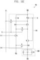
- FIGS. 12 A to 12 C are schematic circuit diagrams illustrating different embodiments of a pixel of FIG. 11 .
- FIG. 14 is a schematic sectional diagram taken along line III-III′ of FIG. 13 .
- first”, “second”, etc. may be used herein to describe various elements, these elements should not be limited by these terms. It will be further understood that the terms “comprise”, “include”, “have”, etc. when used herein, specify the presence of stated features, integers, steps, operations, elements, components, and/or combinations thereof, but do not preclude the presence or addition of one or more other features, integers, steps, operations, elements, components, and/or combinations thereof. Furthermore, when a first part such as a layer, a film, a region, or a plate is disposed “on”, etc., a second part, the first part may be not only directly on the second part but a third part may intervene between them. Furthermore, concepts relating to “position”, “direction”, etc. used in the following description are relative concepts, and it should be noted that terms relating thereto may be reversed, etc., depending on a view angle or direction.
- a singular form may include a plural form.
- the term “and/or” is intended to include any combination of the terms “and” and “or” for the purpose of its meaning and interpretation.
- “A and/or B” may be understood to mean “A, B, or A and B.”
- the terms “and” and “or” may be used in the conjunctive or disjunctive sense and may be understood to be equivalent to “and/or.”
- overlap may include layer, stack, face or facing, extending over, extending under, covering or partly covering or any other suitable term as would be appreciated and understood by those of ordinary skill in the art.
- overlap may include apart from or set aside from or offset from and any other suitable equivalents as would be appreciated and understood by those of ordinary skill in the art.
- At least one of is intended to include the meaning of “at least one selected from the group of” for the purpose of its meaning and interpretation.
- at least one of A and B may be understood to mean “A, B, or A and B.”
- FIGS. 1 A, 1 B, 2 A, 2 B, 3 A, and 3 B are schematic perspective diagrams and schematic sectional diagrams illustrating light emitting elements LD in accordance with embodiments of the disclosure.
- FIGS. 1 A to 3 B illustrate cylindrical rod-type light emitting elements LD, the kind and/or shape of the light emitting elements LD in accordance with the disclosure is not limited thereto.
- a light emitting element LD in accordance with an embodiment of the disclosure may include a first conductive semiconductor layer 11 , a second conductive semiconductor layer 13 , and an active layer 12 interposed between the first and second conductive semiconductor layers 11 and 13 .
- the light emitting element LD may be configured of a stacked body formed by successively stacking the first conductive semiconductor layer 11 , the active layer 12 , and the second conductive semiconductor layer 13 on each other.
- the light emitting element LD may be provided in the form of a rod extending in a direction. If the direction in which the light emitting element LD extends is defined as a longitudinal direction (L), the light emitting element LD may have a first end and a second end with respect to the longitudinal direction (L).
- one of the first and second conductive semiconductor layers 11 and 13 may be disposed on the first end of the light emitting element LD, and another of the first and second conductive semiconductor layers 11 and 13 may be disposed on the second end of the light emitting element LD.
- the light emitting element LD may be fabricated in the form of a rod.
- the term “rod-type” embraces a rod-like shape and a bar-like shape such as a cylindrical shape and a prismatic shape extending in a longitudinal direction (e.g., to have an aspect ratio greater than 1), and the cross-sectional shape thereof is not limited to a particular shape.
- the length L of the light emitting element LD may be greater than a diameter D thereof (or a width of the cross-section thereof).
- the light emitting element LD may have a small size corresponding to a nanoscale size to a microscale size, e.g., a diameter D and/or a length L corresponding to a microscale to nanoscale range.
- the size of the light emitting element LD is not limited thereto.
- the size of the light emitting element LD may be changed in various ways depending on design conditions of various devices, e.g., a display device, which employs, as a light source, a light emitting device using a light emitting element LD.
- the first conductive semiconductor layer 11 may include, for example, at least one n-type semiconductor layer.
- the first conductive semiconductor layer 11 may include an n-type semiconductor layer which includes any one or more semiconductor material of InAlGaN, GaN, AlGaN, InGaN, AlN, and InN, and may be doped with a first conductive dopant such as Si, Ge, Sn, or a combination thereof.
- a first conductive dopant such as Si, Ge, Sn, or a combination thereof.
- the material forming the first conductive semiconductor layer 11 is not limited thereto, and the first conductive semiconductor layer 11 may be formed of various other materials.
- the active layer 12 may be disposed on the first conductive semiconductor layer 11 and have a single or multiple quantum well structure.
- a cladding layer (not shown) doped with a conductive dopant may be formed on and/or under the active layer 12 .
- the cladding layer may be formed of an AlGaN layer, an InAlGaN layer, or a combination thereof.
- a material such as AlGaN or AlInGaN may be used to form the active layer 12 , and various other materials may be used to form the active layer 12 .
- the light emitting element LD may emit light by combination of electron-hole pairs in the active layer 12 . Since light emission of the light emitting element LD can be controlled based on the foregoing principle, the light emitting element LD may be used as a light source of various light emitting devices as well as a pixel of the display device.
- the second conductive semiconductor layer 13 may be disposed on the active layer 12 and include a semiconductor layer of a type different from that of the first conductive semiconductor layer 11 .
- the second conductive semiconductor layer 13 may include at least one p-type semiconductor layer.
- the second conductive semiconductor layer 13 may include a p-type semiconductor layer which includes any one or more semiconductor material of InAlGaN, GaN, AlGaN, InGaN, AlN, and InN, and may be doped with a second conductive dopant such as Mg.
- the material forming the second conductive semiconductor layer 13 is not limited thereto, and the second conductive semiconductor layer 13 may be formed of various other materials.
- an insulating film INF may be provided on an outer circumferential surface of the light emitting element LD (e.g., an outer side surface of a cylinder).
- the insulating film INF may be formed on the surface of the light emitting element LD to enclose an outer circumferential surface of at least the active layer 12 .
- the insulating film INF may further enclose at least a portion of each of the first and second conductive semiconductor layers 11 and 13 .
- the insulating film INF may allow the opposite ends of the light emitting element LD that have different polarities to be exposed to the outside.
- the insulating film INF may expose one end of each of the first and second conductive semiconductor layers 11 and 13 that may be disposed on the respective opposite ends of the light emitting element LD with respect to the longitudinal direction (L), e.g., may expose each of the top and bottom surfaces of the cylinder rather than covering it.
- the insulating film INF may include at least one insulating material of SiO 2 , Si 3 N 4 , Al 2 O 3 , and TiO 2 , but it is not limited thereto.
- the material forming the insulating film INF is not limited to a particular material, and the insulating film INF may be formed of well-known various insulating materials.
- the light emitting element LD may further include additional other components as well as the first conductive semiconductor layer 11 , the active layer 12 , and the second conductive semiconductor layer 13 .
- the light emitting element LD may further include at least one fluorescent layer, at least one active layer, at least one semiconductor layer and/or at least one electrode layer disposed on one end of the first conductive semiconductor layer 11 , the active layer 12 , and/or the second conductive semiconductor layer 13 .
- the light emitting element LD may further include at least one electrode layer 14 disposed on one end of the second conductive semiconductor layer 13 .
- the light emitting element LD may further include at least one electrode layer 15 disposed on one end of the first conductive semiconductor layer 11 .
- each of the electrode layers 14 and 15 may be an ohmic contact electrode, but it is not limited thereto. Furthermore, each of the electrode layers 14 and 15 may include metal or a metal oxide. For example, Cr, Ti, Al, Au, Ni, ITO, IZO, ITZO, or an oxide or alloy thereof may be used alone or in combination with each other. In an embodiment, the electrode layers 14 and 15 may be substantially transparent or translucent. Thereby, light generated from the light emitting element LD may be emitted to the outside after passing through the electrode layers 14 and 15 .
- the insulating film INF may at least partially enclose the outer surfaces of the electrode layers 14 and 15 , or may not enclose them. In other words, the insulating film INF may be selectively formed on the surfaces of the electrode layers 14 and 15 . Furthermore, the insulating film INF may be formed to expose the opposite ends of the light emitting element LD that have different polarities, for example, may expose at least an area of each of the electrode layers 14 and 15 . In other embodiments, in an embodiment, the insulating film INF may not be provided.
- the active layer 12 may be prevented from short-circuiting with at least one electrode which is not shown (e.g., at least one contact electrode of contact electrodes connected to the opposite ends of the light emitting element LD), etc. Consequently, the electrical stability of the light emitting element LD may be secured.
- the insulating film INF formed on the surface of the light emitting element LD Furthermore, thanks to the insulating film INF formed on the surface of the light emitting element LD, occurrence of a defect on the surface of the light emitting element LD may be minimized, whereby the lifetime and efficiency of the light emitting element LD may be improved. In case that the insulating film INF is formed on each light emitting element LD, even in case that multiple light emitting elements LD are disposed adjacent to each other, the light emitting elements LD may be prevented from undesirably short-circuiting.
- a surface treatment process may be performed to fabricate the light emitting element LD.
- the light emitting element LD may be surface-treated (e.g., through a coating process) so that, in case multiple light emitting elements LD are mixed with a fluidic solution and supplied to each light emitting area (e.g., a light emitting area of each pixel), the light emitting elements LD can be evenly distributed rather than unevenly aggregating in the solution.
- a light emitting device including the light emitting element LD described above may be used in various devices including a display device which may require a light source.
- multiple subminiature light emitting elements LD may be disposed in each pixel region of a light emitting display panel, thereby forming a light emitting part of each pixel.
- the field of application of the light emitting element LD according to the disclosure is not limited to a display device.
- the light emitting element LD may also be used in various devices such as a lighting device, which may require a light source.
- FIGS. 4 and 5 are respective schematic plan diagrams illustrating light emitting devices in accordance with embodiments of the disclosure.
- FIGS. 4 and 5 illustrate light emitting devices each of which may include first and second power lines PL 1 and PL 2 or may be electrically connected (e.g., directly connected) to the first and second power lines PL 1 and PL 2 .
- the light emitting device according to the disclosure is not limited to the embodiments illustrated in FIGS. 4 and 5 .
- the light emitting device may be electrically connected to the first and/or second power line PL 1 and/or PL 2 via at least one circuit element (e.g., a pixel circuit), an intermediate connection line, or the like.
- a light emitting device in accordance with an embodiment of the disclosure may include a substrate SUB, a first partition wall PW 1 and a second partition wall PW 2 which may be disposed on the substrate SUB, a first electrode ELT 1 and a second electrode ELT 2 which may be respectively disposed on the first and second partition walls PW 1 and PW 2 , multiple light emitting elements LD disposed between the first and second electrodes ELT 1 and ELT 2 , and a first contact electrode CNE 1 and a second contact electrode CNE 2 which respectively electrically connect first and second ends EP 1 and EP 2 of the light emitting elements LD to the first and second electrodes ELT 1 and ELT 2 .
- the light emitting device is not limited to the embodiments illustrated in FIGS. 4 and 5 .
- at least one light emitting area EMA included in the light emitting device may include only a single light emitting element LD.
- the light emitting device may further include a first connection electrode CNL 1 which connects the first electrode ELT 1 to the first power line PL 1 , and a second connection electrode CNL 2 which connects the second electrode ELT 2 to the second power line PL 2 .
- the first and second connection electrodes CNL 1 and CNL 2 may be respectively and integrally connected to the first and second electrodes ELT 1 and ELT 2 , or electrically connected to the first and second electrodes ELT 1 and ELT 2 via at least one contact hole or the like.
- each of the first and second connection electrodes CNL 1 and CNL 2 may be regarded as being an area of a corresponding electrode of the first and second electrodes ELT 1 and ELT 2 .
- the substrate SUB may form a base component of the light emitting device and be a rigid substrate or a flexible substrate.
- the substrate SUB may be a rigid substrate made of glass or reinforced glass, or a flexible substrate formed of a thin film made of plastic, metal, or a combination thereof.
- the substrate SUB may be a transparent substrate, but it is not limited thereto.
- the substrate SUB may be a translucent substrate, an opaque substrate, or a reflective substrate.
- the material or property of the substrate SUB is not particularly limited.
- the first partition wall PW 1 and the second partition wall PW 2 may be disposed in an area on the substrate SUB, e.g., in a light emitting area EMA, at positions spaced apart from each other.
- the first and second partition walls PW 1 and PW 2 may be disposed on the same layer of the substrate SUB at positions spaced apart from each other by a distance in a first direction DR 1 (e.g., a lateral direction), and each extend in a second direction DR 2 (e.g., a vertical direction) intersecting with the first direction DR 1 .
- the first and second partition walls PW 1 and PW 2 may have substantially the same structure, shape, and/or height, but the disclosure is not limited thereto.
- the first electrode ELT 1 and the second electrode ELT 2 may be respectively disposed on the first partition wall PW 1 and the second partition wall PW 2 and respectively protrude in shapes corresponding to the first and second partition walls PW 1 and PW 2 .
- the first and second electrodes ELT 1 and ELT 2 may be spaced apart from each other by a distance in the first direction DR 1 , and each may extend in the second direction DR 2 intersecting with the first direction DR 1 .
- first and second electrodes ELT 1 and ELT 2 may be disposed in parallel to face each other in the first direction DR 1 , in at least one area on the substrate SUB (e.g., in at least light emitting area EMA), and extend in the second direction DR 2 intersecting with the first direction DR 1 .
- first and second electrodes ELT 1 and ELT 2 may be disposed on the same layer and/or height, but the disclosure is not limited thereto.
- the shapes and/or mutual arrangement relationship of the first and second electrodes ELT 1 and ELT 2 may be changed in various ways.
- the first electrode ELT 1 may be electrically connected to the first power line PL 1 through the first connection electrode CNL 1 .
- the first electrode ELT 1 and the first connection electrode CNL 1 may extend in different directions. For example, in case that the first connection electrode CNL 1 extends in the first direction DR 1 , the first electrode ELT 1 may extend in the second direction DR 2 intersecting with the first direction DR 1 .
- the first electrode ELT 1 may be integrally connected with the first connection electrode CNL 1 .
- the first electrode ELT 1 may be formed to diverge in one way from the first connection electrode CNL 1 .
- the disclosure is not limited thereto.
- the first electrode ELT 1 and the first connection electrode CNL 1 may be separately formed and electrically connected to each other through at least one contact hole, via hole, or the like.
- the first electrode ELT 1 and/or the first connection electrode CNL 1 may be integrally connected with the first power line PL 1 .
- the first electrode ELT 1 and/or the first connection electrode CNL 1 may be formed separately from the first power line PL 1 and electrically connected to the first power line PL 1 via at least one contact hole and/or at least one circuit element. Hence, first power to be supplied to the first power line PL 1 may be transmitted to the first electrode ELT 1 .
- the second electrode ELT 2 may be electrically connected to the second power line PL 2 through the second connection electrode CNL 2 .
- the second electrode ELT 2 and the second connection electrode CNL 2 may extend in different directions. For example, in case that the second connection electrode CNL 2 extends in the first direction DR 1 , the second electrode ELT 2 may extend in the second direction DR 2 intersecting with the first direction DR 1 .
- the second electrode ELT 2 may be integrally connected with the second connection electrode CNL 2 .
- the second electrode ELT 2 may be formed to diverge in one way from the second connection electrode CNL 2 .
- the disclosure is not limited thereto.
- the second electrode ELT 2 and the second connection electrode CNL 2 may be separately formed and electrically connected to each other through at least one contact hole, via hole, or the like.
- the second electrode ELT 2 and/or the second connection electrode CNL 2 may be integrally connected with the second power line PL 2 .
- the second electrode ELT 2 and/or the second connection electrode CNL 2 may be formed separately from the second power line PL 2 and electrically connected to the second power line PL 2 via at least one contact hole and/or at least one circuit element. Hence, second power to be supplied to the second power line PL 2 may be transmitted to the second electrode ELT 2 .
- the first power supply and the second power supply may have different potentials. For example, a difference in potential between the first power supply and the second power supply may be equal to or greater than a threshold voltage of the light emitting elements LD.
- the first power supply and the second power supply may have potentials enabling at least one light emitting element LD disposed between the first and second electrodes ELT 1 and ELT 2 to be connected in a forward direction.
- the voltage between the first power supply and the second power supply may have a value enabling at least one light emitting element LD included in the light emitting device to emit light.
- the light emitting elements LD may be connected in parallel with each other between the first electrode ELT 1 and the second electrode ELT 2 .
- the light emitting elements LD may be arranged in the first direction DR 1 , e.g., in the lateral direction, between the first and second electrodes ELT 1 and ELT 2 in an area in which the first electrode ELT 1 and the second electrode ELT 2 may be disposed to face each other.
- an end of each of the light emitting elements LD may overlap at least the first contact electrode CNE 1 .
- the first ends EP 1 of the light emitting elements LD may overlap the first electrode ELT 1 and the first contact electrode CNE 1 .
- the first ends EP 1 of the light emitting elements LD may overlap only the first contact electrode CNE 1 without overlapping the first electrode ELT 1 .
- the first ends EP 1 of the light emitting elements LD may be electrically connected to the first electrode ELT 1 through the first contact electrode CNE 1 .
- another end of each of the light emitting elements LD may overlap at least the second contact electrode CNE 2 .
- the second ends EP 2 of the light emitting elements LD may overlap the second electrode ELT 2 and the second contact electrode CNE 2 .
- the second ends EP 2 of the light emitting elements LD may overlap only the second contact electrode CNE 2 without overlapping the second electrode ELT 2 .
- the second ends EP 2 of the light emitting elements LD may be electrically connected to the second electrode ELT 2 through the second contact electrode CNE 2 .
- At least one of the opposite ends of the light emitting elements LD may be brought into direct contact with the first or second electrode ELT 1 or ELT 2 and thus be electrically connected to the first or second electrode ELT 1 or ELT 2 .
- FIGS. 4 and 5 illustrate that the light emitting elements LD may be uniformly oriented in any one direction, e.g., in the first direction DR 1 , the disclosure is not limited thereto.
- at least one of the light emitting elements LD may be disposed in a diagonal direction between the first and second electrodes ELT 1 and ELT 2 or may not be properly connected between the first electrode ELT 1 and the second electrode ELT 2 .
- each of the light emitting elements LD may be formed of a rod-type light emitting diode which may be made of material having an inorganic crystal structure and have a subminiature size, e.g., ranging from the nanoscale to the microscale.
- each light emitting element LD may be a subminiature rod-type light emitting diode which has a diameter D and/or a length L ranging from the nanoscale to the microscale, as illustrated in FIGS. 1 A to 3 B .
- the light emitting elements LD may be prepared in a diffused form in a solution, and supplied to a light emitting area EMA defined in the light emitting device by an inkjet printing scheme, a slit coating scheme, or the like.
- the light emitting elements LD may be mixed with a volatile solvent and dropped onto each light emitting area EMA.
- the first power and the second power are respectively applied to the first and second electrodes ELT 1 and ELT 2 through the first and second power lines PL 1 and PL 2 , an electric field may be formed between the first and second electrodes ELT 1 and ELT 2 , whereby the light emitting elements LD may be self-aligned between the first and second electrodes ELT 1 and ELT 2 .
- the solvent may be removed by a volatilization scheme or other schemes.
- the light emitting elements LD may be reliably arranged between the first and second electrodes ELT 1 and ELT 2 .
- the first contact electrode CNE 1 and the second contact electrode CNE 2 may be respectively formed on the opposite ends of the light emitting elements LD, e.g., on the first end EP 1 and the second end EP 2 , the light emitting elements LD may be more reliably connected between the first and second electrodes ELT 1 and ELT 2 .
- the first contact electrode CNE 1 may be formed to cover both the first ends EP 1 of the light emitting elements LD and at least an area of the first electrode ELT 1 , whereby the first ends EP 1 of the light emitting elements LD may be physically and/or electrically connected to the first electrode ELT 1 .
- the second contact electrode CNE 2 may be formed to cover both the second ends EP 2 of the light emitting elements LD and at least an area of the second electrode ELT 2 , whereby the second ends EP 2 of the light emitting elements LD may be physically and/or electrically connected to the second electrode ELT 2 .
- the first power is applied to the first ends EP 1 of the light emitting elements LD via the first power line PL 1 , the first electrode ELT 1 , etc.
- the second power is applied to the second ends EP 2 of the light emitting elements LD via the second power line PL 2 , the second electrode ELT 2 , etc.
- at least one light emitting element LD that is connected in the forward direction between the first and second electrodes ELT 1 and ELT 2 may emit light. Consequently, the light emitting device may emit light.
- the light emitting device may include at least one groove GRV extending in the first direction DR 1 intersecting with the first and second electrodes ELT 1 and ELT 2 (e.g., at right angles) in at least an area including the light emitting area EMA.
- the light emitting device may include multiple grooves GRV formed in an insulating layer disposed between the substrate SUB and the light emitting elements LD.
- the grooves GRV may be arranged in parallel to each other in the corresponding light emitting area EMA in the second direction DR 2 intersecting with the first direction DR 1 .
- the disclosure is not limited to the foregoing structure and, for example, the shape and/or arrangement of the grooves GRV formed in each light emitting area EMA may be changed in various ways.
- the light emitting device may include light emitting elements LD each of which may be disposed on any one groove GRV such that the light emitting element LD may be disposed between the first and second electrodes ELT 1 and ELT 2 .
- the light emitting elements LD distributed in each light emitting area EMA may be disposed between the first and second electrodes ELT 1 and ELT 2 such that they may be located in any one of the grooves GRV formed in the corresponding light emitting area EMA.
- At least one groove GRV extending in a direction intersecting with the first and second electrodes ELT 1 and ELT 2 may be formed in the light emitting device.
- light emitting elements LD may be supplied into each light emitting area EMA. Consequently, the light emitting elements LD may be aligned between the first and second electrodes ELT 1 and ELT 2 with more uniform directionality. Therefore, according to the foregoing embodiment, the light emitting elements LD may be more uniformly aligned in the light emitting area EMA.
- FIG. 6 is a schematic perspective diagram illustrating first and second electrodes ELT 1 and ELT 2 , a groove GRV, and light emitting elements LD in accordance with an embodiment of the disclosure.
- FIG. 6 schematically illustrates mutual arrangement relationship of the first and second electrodes ELT 1 and ELT 2 , the groove GRV, and the light emitting elements LD, focused on an area of the light emitting area EMA illustrated in FIG. 4 (e.g., an area disposed between the first and second electrodes ELT 1 and ELT 2 that face each other).
- like reference numerals are used to designate components similar or equal to those of the embodiments of FIGS. 4 and 5 , and detailed explanation thereof will be omitted.
- a light emitting device in accordance with an embodiment of the disclosure may further include an insulating layer INS formed on the substrate SUB on which the first and second electrodes ELT 1 and ELT 2 may be formed.
- the insulating layer INS may include at least one groove GRV extending in the first direction DR 1 intersecting with the extension direction (e.g., the second direction DR 2 ) of the first and second electrodes ELT 1 and ELT 2 .
- Multiple light emitting elements LD may be disposed on the at least one groove GRV.
- each groove GRV may have an overall shape extending in the first direction DR 1 , and discontinuously extend in the first direction DR 1 in a shape in which the groove GRV may be partially disconnected or open on an area corresponding to each contact portion.
- each groove GRV may continuously extend in the first direction DR 1 in at least an area between the first and second electrodes ELT 1 and ELT 2 , and be partially removed in an area over each of the first and second electrodes ELT 1 and ELT 2 .
- the insulating layer INS may include at least one organic insulating layer. Furthermore, the insulating layer INS may selectively further include at least one inorganic insulating layer.
- the insulating layer INS may be formed of an organic insulating layer in at least an upper area in which the groove GRV may be formed.
- light emitting elements LD disposed in at least one groove GRV may have an arrangement shape corresponding to the shape of the corresponding groove GRV.
- each of the light emitting elements LD may be a rod-type light emitting diode.
- the rod-type light emitting diode may be arranged to have a length L extending in the first direction DR 1 in which the corresponding groove GRV extends.
- each groove GRV may be formed to stably receive at least one light emitting element LD located thereon.
- each groove GRV may have, in the second direction DR 2 , a width W greater than a diameter D or a width of each of the light emitting elements LD.
- each groove GRV may have, in a third direction DR 3 perpendicular to the first and second directions DR 1 and DR 2 , a depth DP corresponding to a half or more of the thickness of each of the light emitting elements LD (the diameter D in the case where the light emitting elements LD each have a cylindrical shape), but the depth DP of the groove GRV is not limited thereto.
- the groove GRV extending in the first direction DR 1 intersecting with the first and second electrodes ELT 1 and ELT 2 may be formed in the insulating layer INS disposed on the first and second electrodes ELT 1 and ELT 2 , the light emitting elements LD may be supplied onto the insulating layer INS.
- the light emitting elements LD may be aligned between the first and second electrodes ELT 1 and ELT 2 with more uniform directionality by the groove GRV in the surface of the insulating layer INS.
- the number of light emitting elements LD disposed in the lateral direction along the first direction DR 1 between the first and second electrodes ELT 1 and ELT 2 among the light emitting elements LD supplied to the light emitting area EMA may be increased.
- FIGS. 7 and 8 are schematic sectional diagrams illustrating different embodiments of a sectional diagram taken along line I-I′ of FIG. 4 , and particularly, illustrate different embodiments related to the shapes of the first and second partition walls PW 1 and PW 2 .
- FIG. 9 is a schematic sectional diagram illustrating an embodiment of a sectional diagram taken along line II-II′ of FIG. 5 , and particularly, illustrates an embodiment where the light emitting elements LD may not overlap the first and second electrodes ELT 1 and ELT 2 .
- the light emitting device in accordance with an embodiment of the disclosure may include a substrate SUB, first and second electrodes ELT 1 and ELT 2 disposed on the substrate SUB, multiple light emitting elements LD connected between the first and second electrodes ELT 1 and ELT 2 , at least one insulating layer INS disposed between the light emitting elements LD and the substrate SUB on which the first and second electrodes ELT 1 and ELT 2 may be formed, and first and second contact electrodes CNE 1 and CNE 2 that respectively connect first and second ends EP 1 and EP 2 of the light emitting elements LD to the first and second electrodes ELT 1 and ELT 2 .
- the light emitting device may further include at least one of a buffer layer BFL disposed between the substrate SUB and the first and second electrodes ELT 1 and ELT 2 , a first partition wall PW 1 disposed between the substrate SUB and an area of the first electrode ELT 1 , a second partition wall PW 2 disposed between the substrate SUB and an area of the second electrode ELT 2 , a first insulating pattern INP 1 disposed over areas of the light emitting elements LD, a second insulating pattern INP 2 disposed over the first contact electrode CNE 1 , and an overcoat layer OC that covers one surface of the substrate SUB on which the first and second electrodes ELT 1 and ELT 2 , the light emitting elements LD, and the first and second contact electrodes CNE 1 and CNE 2 , etc. may be formed.
- a buffer layer BFL disposed between the substrate SUB and the first and second electrodes ELT 1 and ELT 2
- a first partition wall PW 1 disposed between the substrate SUB and an area of
- the substrate SUB may form a base component of the light emitting device and be a rigid substrate or a flexible substrate. Furthermore, the substrate SUB may be a transparent substrate, but it is not limited thereto. In other words, in the disclosure, the material or property of the substrate SUB is not particularly limited.
- the buffer layer BFL may be formed on one surface of the substrate SUB.
- the buffer layer BFL may prevent impurities from diffusing into electrodes, lines, and/or a circuit element that may be disposed on the buffer layer BFL.
- the buffer layer BFL may be formed of a single layer, or may be formed of multiple layers having at least two layers. In the case where the buffer layer BFL has a multilayer structure, the respective layers may be formed of the same material or different materials. In an embodiment, the buffer layer BFL may be omitted.
- the first partition wall PW 1 and the second partition wall PW 2 may be disposed on the one surface of the substrate SUB on which the buffer layer BFL may be formed. In an embodiment, the first and second partition walls PW 1 and PW 2 may be disposed on a surface of the substrate SUB at positions spaced apart from each other. For example, the first and second partition walls PW 1 and PW 2 may be disposed on the same layer on the substrate SUB at positions spaced apart from each other by a distance. In an embodiment, the first and second partition walls PW 1 and PW 2 may have substantially the same structure, shape, and/or height, but the disclosure is not limited thereto.
- each of the first and second partition walls PW 1 and PW 2 may include an insulating material having an inorganic material and/or an organic material. Furthermore, each of the first and second partition walls PW 1 and PW 2 may have a single-layer structure or a multi-layer structure. In other words, the material and/or the stacked structure of each of the first and second partition walls PW 1 and PW 2 may be changed in various ways rather than being particularly limited.
- each of the first and second partition walls PW 1 and PW 2 may have various shapes.
- each of the first and second partition walls PW 1 and PW 2 may have the cross-sectional shape of a trapezoid that may be reduced in width from a bottom to a top thereof.
- each of the first and second partition walls PW 1 and PW 2 may have a semi-circular or semi-elliptical cross-section the width of which may be gradually reduced upward.
- the shape of each of the first and second partition walls PW 1 and PW 2 may be changed in various ways rather than being particularly limited.
- at least one of the first and second partition walls PW 1 and PW 2 may be omitted or changed in position.
- the first electrode ELT 1 and the first contact electrode CNE 1 may be disposed over the first partition wall PW 1 .
- the second electrode ELT 2 and the second contact electrode CNE 2 may be disposed over the second partition wall PW 2 .
- At least one electrode and/or insulating layer disposed over each of the first and second partition walls PW 1 and PW 2 may have a shape corresponding to the shape of a corresponding first or second partition wall PW 1 or PW 2 , but the disclosure is not limited thereto.
- the first and second electrodes ELT 1 and ELT 2 may be disposed at positions spaced apart from each other on the substrate SUB on which the first and second partition walls PW 1 and PW 2 may be disposed.
- the first electrode ELT 1 may be disposed on the first partition wall PW 1 to cover the first partition wall PW 1 .
- the second electrode ELT 2 may be disposed on the second partition wall PW 2 to cover the second partition wall PW 2 .
- any one of the first and second electrodes ELT 1 and ELT 2 may be an anode electrode, and another may be a cathode electrode.
- the first and second electrodes ELT 1 and ELT 2 may respectively have shapes corresponding to those of the first and second partition walls PW 1 and PW 2 .
- the first electrode ELT 1 may have an inclined surface or a curved surface corresponding to the shape of the first partition wall PW 1
- the second electrode ELT 2 may have an inclined surface or a curved surface corresponding to the shape of the second partition wall PW 2 .
- the first and second partition walls PW 1 and PW 2 may not be provided in the light emitting device.
- Each of the first and second electrodes ELT 1 and ELT 2 may have a substantially planar shape.
- the first and second electrodes ELT 1 and ELT 2 may be disposed on the same plane on the substrate SUB and have substantially the same height. As such, if the first and second electrodes ELT 1 and ELT 2 have the same height, the light emitting elements LD may be more reliably connected between the first and second electrodes ELT 1 and ELT 2 .
- the disclosure is not limited thereto.
- the shapes, the structures, and/or the mutual disposition relationship of the first and second electrodes ELT 1 and ELT 2 may be changed in various ways.
- each of the first and second electrodes ELT 1 and ELT 2 may have a single-layer structure or a multilayer structure, and the cross-sectional structure thereof is not particularly limited.
- the first electrode ELT 1 may have a multilayer structure including a first reflective electrode REF 1 and a first conductive capping layer CPL 1 .
- the second electrode ELT 2 may have a multilayer structure including a second reflective electrode REF 2 and a second conductive capping layer CPL 2 .
- Each of the first and second reflective electrodes REF 1 and REF 2 may be formed of conductive material having a reflectivity.
- each of the first and second reflective electrodes REF 1 and REF 2 may include at least one of metals such as Ag, Mg, Al, Pt, Pd, Au, Ni, Nd, Ir, Cr, or an alloy thereof; however, the disclosure is not limited thereto.
- Each of the first and second reflective electrodes REF 1 and REF 2 may be formed of various reflective conductive materials.
- the first and second reflective electrodes REF 1 and REF 2 may enable light emitted from the opposite ends of each of the light emitting elements LD, e.g., the first and second ends EP 1 and EP 2 of the light emitting elements LD, to travel in a direction (e.g., in a frontal direction) in which an image may be displayed.
- each of the first and second reflective electrodes REF 1 and REF 2 has an inclination or curvature corresponding to the shape of a corresponding one of the first and second partition walls PW 1 and PW 2 , light emitted from the first and second ends EP 1 and EP 2 of each of the light emitting elements LD may be reflected by the first and second reflective electrodes REF 1 and REF 2 , whereby the light may travel more reliably in the frontal direction of the light emitting device (e.g., in an upward direction of the substrate SUB). Thereby, the efficiency of light emitted from the light emitting elements LD may be enhanced.
- each of the first and second partition walls PW 1 and PW 2 may also function as a reflective member.
- the first and second partition walls PW 1 and PW 2 along with the first and second reflective electrodes REF 1 and REF 2 provided on the first and second partition walls PW 1 and PW 2 , may function as reflective components for enhancing the efficiency of light emitted from each of the light emitting elements LD.
- the first and second conductive capping layers CPL 1 and CPL 2 may be respectively selectively disposed over the first and second reflective electrodes REF 1 and REF 2 .
- the first conductive capping layer CPL 1 may be disposed over the first reflective electrode REF 1 to cover the first reflective electrode REF 1 .
- the second conductive capping layer CPL 2 may be provided over the second reflective electrode REF 2 to cover the second reflective electrode REF 2 .
- Each of the first and second conductive capping layers CPL 1 and CPL 2 may be formed of transparent conductive material such as ITO, IZO, or a combination thereof, so as to minimize loss of light emitted from the light emitting element LD.
- transparent conductive material such as ITO, IZO, or a combination thereof.
- the disclosure is not limited thereto.
- the material of the first and second conductive capping layers CPL 1 and CPL 2 may be changed in various ways.
- the first and second conductive capping layers CPL 1 and CPL 2 may prevent the first and second reflective electrodes REF 1 and REF 2 from being damaged by defects which may occur during a process of fabricating the light emitting device, and may reinforce adhesive force between the substrate SUB and the first and second reflective electrodes REF 1 and REF 2 .
- at least one of the first and second conductive capping layers CPL 1 and CPL 2 may be omitted.
- the insulating layer INS may be formed on the substrate SUB on which the first and second electrodes ELT 1 and ELT 2 may be disposed.
- at least one groove GRV extending in the first direction DR 1 intersecting with the second direction DR 2 in which the first and second electrodes ELT 1 and ELT 2 extend may be formed on the surface of the insulating layer INS at least between the first and second electrodes ELT 1 and ELT 2 .
- the insulating layer INS may include at least one organic insulating layer. Furthermore, the insulating layer INS may selectively further include at least one inorganic insulating layer.
- the insulating layer INS may include at least one inorganic insulating layer (hereinafter, referred to as “first insulating layer INS 1 ”) disposed on the substrate SUB on which the first and second electrodes ELT 1 and ELT 2 may be formed, and an organic insulating layer (hereinafter, referred to as “second insulating layer INS 2 ”) disposed on the first insulating layer INS 1 .
- the first insulating layer INS 1 may include, e.g., silicon nitride SiN x , but the material for forming the first insulating layer INS 1 is not limited thereto.
- the first insulating layer INS 1 may be configured of at least one of various known inorganic insulating layer materials.
- the first insulating layer INS 1 may be configured of a single layer or multiple layers, and the sectional structure thereof is not particularly limited.
- the second insulating layer INS 2 may include polymeric organic material, and be formed to have flexibility.
- the second insulating layer INS 2 may be a polyimide coating layer formed of polyimide, but the material for forming the second insulating layer INS 2 is not limited thereto.
- the second insulating layer INS 2 may be formed of at least one of various known organic insulating layer materials.
- the second insulating layer INS 2 may be configured of a single layer or multiple layers, and the sectional structure thereof is not particularly limited.
- At least one groove GRV extending in the first direction DR 1 intersecting with the first and second electrodes ELT 1 and ELT 2 may be formed in the surface of the second insulating layer INS 2 .
- the groove GRV may be formed by a rubbing scheme, but the method of forming the groove GRV is not limited thereto. Thanks to the groove GRV formed in the second insulating layer INS 2 , the light emitting elements LD may be disposed over the second insulating layer INS 2 with more uniform directionality. In other words, in an embodiment, the second insulating layer INS 2 may form a polymer orientation layer.
- the insulating layer INS may include first and second contact portions CNT 1 and CNT 2 respectively allowing areas of the first and second electrodes ELT 1 and ELT 2 to be exposed.
- each of the first and second insulating layers INS 1 and INS 2 may be partially open so that the first and second electrodes ELT 1 and ELT 2 may be exposed over areas of the first and second electrodes ELT 1 and ELT 2 .
- multiple light emitting elements LD may be disposed on the substrate SUB on which the insulating layer INS may be disposed.
- the light emitting elements LD may be disposed over the second insulating layer INS 2 and disposed between the first electrode ELT 1 and the second electrode ELT 2 in a plan view of the substrate SUB.
- Each of the light emitting elements LD may have a first end EP 1 and a second end EP 2 on respective opposite sides thereof in the longitudinal direction (L).
- the light emitting elements LD may be horizontally disposed on a surface of the substrate SUB. Furthermore, the light emitting elements LD may be arranged in the lateral direction between the first and second electrodes ELT 1 and ELT 2 such that the longitudinal direction (L) thereof corresponds to the first direction DR 1 .
- the first ends EP 1 of the light emitting elements LD may be disposed to face the first electrode ELT 1 .
- the second ends EP 2 of the light emitting elements LD may be disposed to face the second electrode ELT 2 .
- first and second ends EP 1 and EP 2 of the light emitting elements LD may respectively overlap the first and second electrodes ELT 1 and ELT 2 , as illustrated in FIGS. 7 and 8 .
- first and second ends EP 1 and EP 2 of the light emitting elements LD may respectively overlap only the first and second contact electrodes CNE 1 and CNE 2 without overlapping the first and second electrodes ELT 1 and ELT 2 , as illustrated in FIG. 9 .
- the first and second ends EP 1 and EP 2 of the light emitting elements LD may be electrically connected to the first and second electrodes ELT 1 and ELT 2 through the first and second contact electrodes CNE 1 and CNE 2 , respectively.
- the light emitting elements LD may be aligned between the first and second electrodes ELT 1 and ELT 2 to have more uniform directionality, by a combination of a physical alignment scheme using the groove GRV formed in the surface of the second insulating layer INS 2 and an electrical alignment scheme using an electric field formed by applying a voltage between the first and second electrodes ELT 1 and ELT 2 .
- the light emitting elements LD may be induced to be disposed in the groove GRV, and may be arranged such that the first and second ends EP 1 and EP 2 thereof respectively face the first and second electrodes ELT 1 and ELT 2 .
- the light emitting elements LD may be arranged between the first and second electrodes ELT 1 and ELT 2 such that each light emitting element LD may be disposed on any one groove GRV in the first direction DR 1 in which the groove GRV extends.
- FIGS. 4 to 9 illustrate only valid light emitting elements where the first and second ends EP 1 and EP 2 of each of the light emitting elements may be connected to the first and second electrodes ELT 1 and ELT 2 .
- the light emitting device may not only include the valid light emitting elements but may also include at least one light emitting element (not illustrated) that may not be completely connected between the first and second electrodes ELT 1 and ELT 2 .
- the light emitting elements LD supplied to the light emitting area EMA of the light emitting device may be aligned between the first and second electrodes ELT 1 and ELT 2 and electrically connected to the first and second electrodes ELT 1 and ELT 2 .
- the number of light emitting elements LD aligned between the first and second electrodes ELT 1 and ELT 2 with uniform directionality may be further increased.
- the first and second contact electrodes CNE 1 and CNE 2 , etc. may be disposed on the substrate SUB on which the light emitting elements LD may be disposed.
- the first and second contact electrodes CNE 1 and CNE 2 may electrically connect the light emitting elements LD between the first and second electrodes ELT 1 and ELT 2 .
- the first contact electrode CNE 1 may be formed to cover not only the first ends EP 1 of the light emitting elements LD but also the first contact portion CNT 1 .
- the first contact electrode CNE 1 may be electrically connected to the light emitting elements LD by coming into contact with the light emitting elements LD on the first ends EP 1 of the light emitting elements LD, and electrically connected to the first electrode ELT 1 by coming into contact with the first electrode ELT 1 on the first contact portion CNT 1 .
- the first ends EP 1 of the light emitting elements LD and the first electrode ELT 1 may be electrically connected to each other through the first contact electrode CNE 1 .
- the second contact electrode CNE 2 may be formed to cover not only the second ends EP 2 of the light emitting elements LD but also the second contact portion CNT 2 .
- the second contact electrode CNE 2 may be electrically connected to the light emitting elements LD by coming into contact with the light emitting elements LD on the second ends EP 2 of the light emitting elements LD, and electrically connected to the second electrode ELT 2 by coming into contact with the second electrode ELT 2 on the second contact portion CNT 2 .
- the second ends EP 2 of the light emitting elements LD and the second electrode ELT 2 may be electrically connected to each other through the second contact electrode CNE 2 .
- the light emitting device may include at least one insulating pattern (or an insulating layer) provided to secure electrical stability (e.g., insulating characteristics) between the first and second contact electrodes CNE 1 and CNE 2 .
- the light emitting device may include a first insulating pattern INP 1 disposed on areas of the light emitting elements LD between the first and second contact electrodes CNE 1 and CNE 2 , and a second insulating pattern INP 2 that covers upper portions of the first insulating pattern INP 1 and the first contact electrode CNE 1 .
- the first insulating pattern INP 1 may be disposed over the light emitting elements LD to cover at least areas of the light emitting elements LD, and may be formed to allow the first and second ends EP 1 and EP 2 of the light emitting elements LD to be exposed.
- the first insulating pattern INP 1 may include at least one organic insulating layer and/or inorganic insulating layer, and the material or properties thereof are not particularly limited.
- the first insulating pattern INP 1 may include, e.g., silicon nitride SiN x , but the material for forming the first insulating pattern INP 1 is not limited thereto.
- the first insulating pattern INP 1 may be configured of a single layer or multiple layers, and the sectional structure thereof is not particularly limited.
- the first insulating pattern INP 1 may be formed of multiple layers including a lower pattern layer LPT and an upper pattern layer UPT that may be formed of the same material or different materials, but the disclosure is not limited thereto.
- the first contact electrode CNE 1 described above may be disposed on the substrate SUB on which the first insulating pattern INP 1 , etc. may be formed. In an embodiment, one end of the first contact electrode CNE 1 may be disposed on one end of the first insulating pattern INP 1 that may be located on the first ends EP 1 of the light emitting elements LD.
- the second insulating pattern INP 2 may be formed, to cover the upper portions of the first insulating pattern INP 1 and the first contact electrode CNE 1 , on the substrate SUB on which the first insulating pattern INP 1 and the first contact electrode CNE 1 may be formed.
- the second insulating pattern INP 2 may be formed to allow the second ends EP 2 of the light emitting elements LD to be exposed.
- the second insulating pattern INP 2 may include at least one organic insulating layer and/or inorganic insulating layer, and the material or properties thereof are not particularly limited.
- the second insulating pattern INP 2 may include material equal to or different from that of the first insulating pattern INP 1 .
- the second insulating pattern INP 2 may include, e.g., silicon nitride SiN x , but the material for forming the second insulating pattern INP 2 is not limited thereto.
- the second insulating pattern INP 2 may be configured of a single layer or multiple layers, and the sectional structure thereof is not particularly limited.
- the second contact electrode CNE 2 described above may be disposed on the substrate SUB on which the second insulating pattern INP 2 , etc. may be formed. In an embodiment, one end of the second contact electrode CNE 2 may be disposed on one end of the second insulating pattern INP 2 that may be adjacent to the second ends EP 2 of the light emitting elements LD.
- An overcoat layer OC may be disposed on the substrate SUB on which the first and second contact electrodes CNE 1 and CNE 2 , etc. may be disposed.
- the overcoat layer OC may be formed of a single layer or multiple layers.
- the overcoat layer OC may include a thin film encapsulation layer which includes multiple inorganic insulating layers overlapping each other and at least one organic insulating layer interposed between the inorganic insulating layers.
- the material and/or sectional structure of the overcoat layer OC is not particularly limited, and may be changed in various ways.
- the efficiency and uniformity at which the light emitting elements LD may be aligned in the light emitting area EMA may be increased by a combination of the physical alignment scheme and the electrical alignment scheme. Consequently, emission characteristics of the light emitting device, e.g., emission luminance, emission efficiency and/or emission uniformity, can be enhanced.
- FIGS. 10 A to 10 K are schematic sectional diagrams sequentially illustrating a method of fabricating the light emitting device illustrated in FIG. 7 .
- a buffer layer BFL may be formed on one surface of a substrate SUB, and first and second partition walls PW 1 and PW 2 may be formed at positions spaced apart from each other on the substrate SUB on which the buffer layer BFL may be formed.
- the first and second partition walls PW 1 and PW 2 may be formed through a process of forming an insulating layer including inorganic material and/or organic material and/or a patterning process (e.g., a mask process), and may be formed through various types of known processes.
- the first and second partition walls PW 1 and PW 2 may be simultaneously formed using the same material on the same layer (or the same plane) on the substrate SUB, but the disclosure is not limited thereto.
- first and second electrodes ELT 1 and ELT 2 may be formed on the first and second partition walls PW 1 and PW 2 .
- the first and second electrodes ELT 1 and ELT 2 may be formed through a process of forming a conductive layer including at least one conductive material and/or a patterning process, and may be formed through various types of known processes.
- each of the first and second electrodes ELT 1 and ELT 2 may be formed of a single layer or multiple layers.
- the first electrode ELT 1 may be formed of multiple layers including a first reflective electrode REF 1 and a first conductive capping layer CPL 1 .
- the second electrode ELT 2 may be formed of multi-layers including a second reflective electrode REF 2 and a second conductive capping layer CPL 2 .
- the step of forming the first and second electrodes ELT 1 and ELT 2 may include the step of forming the first and second reflective electrodes REF 1 and REF 2 respectively on the first and second partition walls PW 1 and PW 2 , and the step of forming the first and second conductive capping layers CPL 1 and CPL 2 on the first and second reflective electrodes REF 1 and REF 2 .
- the first and second electrodes ELT 1 and ELT 2 may be simultaneously formed on the same layer on the substrate SUB, but the disclosure is not limited thereto. In the case where the first and second electrodes ELT 1 and ELT 2 may be simultaneously formed, the number of mask processes to be used to fabricate the light emitting device may be reduced or minimized.
- At least one insulating layer INS may be formed on the substrate SUB on which the first and second electrodes ELT 1 and ELT 2 may be formed.
- first and second insulating layers INS 1 and INS 2 may be successively formed on the substrate SUB on which the first and second electrodes ELT 1 and ELT 2 may be formed.
- the insulating layer INS may be formed through a deposition process of an insulating layer including inorganic material and/or organic material, and may be formed through various types of known processes.
- the insulating layer INS may be formed of a single layer or multiple layers. For example, after at least one inorganic insulating layer, e.g., the first insulating layer INS 1 , is formed using at least one inorganic material, an organic insulating layer, e.g., the second insulating layer INS 2 , may be formed on the first insulating layer INS 1 using at least one organic material.
- the second insulating layer INS 2 may be formed by, e.g., coating a polymeric organic layer including polyimide, but the material of the second insulating layer INS 2 and/or the method of forming the second insulating layer INS 2 is not limited thereto.
- At least one groove GRV may be formed in the surface of the insulating layer INS e.g., the surface of at least the second insulating layer INS 2 .
- the groove GRV may be formed by a rubbing scheme using a rubbing device RUD.
- the groove GRV may be formed in the surface of the second insulating layer INS 2 by disposing the rubbing device RUD on the second insulating layer INS 2 such that the rubbing device RUD comes into contact with the second insulating layer INS 2 , and pressing the second insulating layer INS 2 while moving the substrate SUB and/or the rubbing device RUD in the first direction DR 1 intersecting with the first and second electrodes ELT 1 and ELT 2 in one way or reciprocating ways at least once.
- the rubbing device RUD may include a roller ROL that is rotatable in at least one direction, and a rubbing cloth RUC wound around the roller ROL.
- At least one of the substrate SUB and the roller ROL is moved in the first direction DR 1 while the rubbing cloth RUC makes contact with the surface of the second insulating layer INS 2 , at least one groove GRV intersecting with the first and second electrodes ELT 1 and ELT 2 may be formed in the surface of the second insulating layer INS 2 .
- the rubbing device RUD may be disposed on the second insulating layer INS 2 , and the second insulating layer INS 2 may be pressed at intervals of a distance.
- grooves GRV extending in parallel to each other in a direction intersecting with the first and second electrodes ELT 1 and ELT 2 may be formed in the surface of the second insulating layer INS 2 .
- the grooves GRV may be simultaneously formed or successively formed.
- multiple light emitting elements LD may be supplied onto the insulating layer INS including the at least one groove GRV, and an electric field may be formed by applying a voltage (e.g., an AC voltage) between the first and second electrodes ELT 1 and ELT 2 .
- the light emitting elements LD may be supplied into a light emitting area EMA by applying a solution with multiple light emitting elements LD dispersed therein to the substrate SUB using an inkjet printing scheme, a slit coating scheme, or the like.
- the scheme of supplying the light emitting elements LD is not limited to the foregoing scheme, and the light emitting elements LD may be supplied to the light emitting area EMA in various other ways.
- the electric field may be formed by applying an AC voltage between the first and second electrodes ELT 1 and ELT 2 , but the type of voltage or signal to be applied between the first and second electrodes ELT 1 and ELT 2 is not limited thereto.
- the light emitting elements LD may be aligned between the first and second electrodes ELT 1 and ELT 2 .
- the light emitting elements LD may be more uniformly aligned in the light emitting area EMA with more uniform directionality by the groove GRV formed in the surface of the insulating layer INS.
- the number of light emitting elements LD uniformly and laterally disposed in the first direction DR 1 between the first and second electrodes ELT 1 and ELT 2 may be increased.
- the first ends EP 1 of the light emitting elements LD may be disposed to face the first electrode ELT 1 .
- the second ends EP 2 of the light emitting elements LD may be disposed to face the second electrode ELT 2 .
- a first insulating pattern INP 1 e.g., a lower pattern layer LPT of the first insulating pattern INP 1
- the lower pattern layer LPT may be formed on areas of the light emitting elements LD such that the first and second ends EP 1 and EP 2 of the light emitting elements LD may be exposed.
- the lower pattern layer LPT may be formed through a process of forming an insulating layer including inorganic material and/or organic material and/or a patterning process (e.g., a mask process), and may be formed through various types of known processes.
- the second insulating layer INS 2 may be etched such that an area of the first insulating layer INS 1 corresponding to each of the first and second electrodes ELT 1 and ELT 2 may be exposed.
- an opening may be formed in the second insulating layer INS 2 over areas of the first and second electrodes ELT 1 and ELT 2 .
- first and second contact portions CNT 1 and CNT 2 may be formed in the insulating layer INS by etching the first insulating layer INS 1 such that an area of each of the first and second electrodes ELT 1 and ELT 2 may be exposed.
- first and second contact portions CNT 1 and CNT 2 may be formed in the insulating layer INS by etching the first insulating layer INS 1 after the second insulating layer INS 2 has been etched, the disclosure is not limited thereto.
- the first and second contact portions CNT 1 and CNT 2 may be formed by etching the first and second insulating layers INS 1 and INS 2 together over an area of each of the first and second electrodes ELT 1 and ELT 2 such that the areas of the first and second electrodes ELT 1 and ELT 2 may be exposed.
- a first contact electrode CNE 1 may be formed on an area of the substrate SUB including the first ends EP 1 of the light emitting elements LD and the first contact portion CNT 1 .
- the first contact electrode CNE 1 may be formed on areas of the light emitting elements LD and the first electrode ELT 1 such that the first contact electrode CNE 1 comes into contact with the first ends EP 1 of the light emitting elements LD and an area of the first electrode ELT 1 .
- a second insulating pattern INP 2 may be formed on the first contact electrode CNE 1 to cover at least the first contact electrode CNE 1 . Furthermore, in an embodiment, at the step of forming the second insulating pattern INP 2 , e.g., at the step of patterning the second insulating pattern INP 2 , an upper pattern layer UPT of the first insulating pattern INP 1 may also be formed by etching together the mask MAS shown in FIG. 10 I . In an embodiment, the upper pattern layer UPT and the second insulating pattern INP 2 may be successively formed.
- a first insulating pattern INP 1 which has a single-layer structure and may be formed of only the lower pattern layer LPT without having the upper pattern layer UPT may be formed by adjusting the position of the mask MAS, or a first insulating pattern INP 1 having a multilayer structure may be formed before the mask MAS may be formed.
- a second contact electrode CNE 2 may be formed on an area of the substrate SUB that includes the second ends EP 2 of the light emitting elements LD and the second contact portion CNT 2 .
- the second contact electrode CNE 2 may be formed on areas of the light emitting elements LD and the second electrode ELT 2 such that the second contact electrode CNE 2 comes into contact with the second ends EP 2 of the light emitting elements LD and an area of the second electrode ELT 2 .
- an overcoat layer OC may be formed on the substrate SUB on which the first and second contact electrodes CNE 1 and CNE 2 may be disposed.
- an overcoat layer OC may be formed on the substrate SUB on which the first and second contact electrodes CNE 1 and CNE 2 may be disposed.
- the second insulating layer INS 2 formed of at least one organic insulating layer may be formed before the light emitting elements LD may be supplied to the light emitting area EMA of the light emitting device. Thereafter, at least one groove GRV may be formed in the second insulating layer INS 2 by a rubbing scheme using the rubbing device RUD.
- each groove GRV may be formed in the first direction DR 1 in which each of the light emitting elements LD is to be aligned.
- the first direction DR 1 may be a direction perpendicular to the first and second electrodes ELT 1 and ELT 2 , but the disclosure is not limited thereto.
- the first direction DR 1 may include not only a direction perpendicular to the first and second electrodes ELT 1 and ELT 2 but also a direction diagonally passing through the first and second electrodes ELT 1 and ELT 2 .
- the first direction DR 1 may include various directions intersecting with the first and second electrodes ELT 1 and ELT 2 .
- the light emitting elements LD may be supplied to the light emitting area EMA. Therefore, the light emitting elements LD or the insulating film INF that encloses the surfaces of the light emitting elements LD may be prevented from being damaged by the rubbing process or the like.
- a voltage may be applied between the first and second electrodes ELT 1 and ELT 2 simultaneously with or after the supply of the light emitting elements LD. Consequently, an electric field may be formed between the first and second electrodes ELT 1 and ELT 2 , whereby the light emitting elements LD may be self-aligned.
- the light emitting elements LD supplied to the light emitting area EMA may be aligned in a physical scheme and an electrical scheme by complexly using the groove GRV formed in the second insulating layer INS 2 through the rubbing process or the like and the electric field formed between the first and second electrodes ELT 1 and ELT 2 .
- the light emitting elements LD may be more uniformly aligned between the first and second electrodes ELT 1 and ELT 2 , and the contact rate between the light emitting elements LD and the first and second electrodes ELT 1 and ELT 2 may be enhanced, compared to a light emitting device of a comparative example using only either a physical or an electrical alignment scheme. Consequently, emission characteristics of the light emitting device including emission luminance, emission efficiency, and/or emission uniformity can be enhanced.
- FIG. 11 is a schematic plan diagram illustrating a display device in accordance with an embodiment of the disclosure.
- FIG. 11 illustrates a display device, particularly, a display panel PNL provided in the display device, as an example of a device capable of using the light emitting device according to the above-described embodiments as a light source.
- FIG. 11 simply illustrates the structure of the display panel PNL, focusing on a display area DA.
- at least one driving circuit e.g., at least one of a scan driver and a data driver
- multiple lines may be further provided on the display panel PNL.
- the display panel PNL in accordance with an embodiment of the disclosure may include a substrate SUB, and pixels PXL disposed on the substrate SUB.
- the substrate SUB may include a display area DA that displays an image, and a non-display area NDA formed in an area other than the display area DA.
- the pixels PXL may be disposed in the display area DA on the substrate SUB.
- the display area DA may be disposed in a central portion of the display panel PNL, and the non-display area NDA may be disposed in a perimeter portion of the display panel PNL in such a way as to enclose the display area DA.
- the locations of the display area DA and the non-display area NDA are not limited thereto, and the locations thereof may be changed.
- the substrate SUB may be a rigid or flexible substrate, and the material or properties thereof are not particularly limited.
- the substrate SUB may be a rigid substrate made of glass or reinforced glass, or a flexible substrate formed of a thin film made of plastic or metal.
- An area on the substrate SUB may be defined as the display area DA in which the pixels PXL may be disposed, and another area thereof may be defined as the non-display area NDA.
- the substrate SUB may include the display area DA including multiple pixel regions on which the respective pixels PXL may be formed, and the non-display area NDA that encloses the display area DA.
- Different kinds of lines and/or internal circuits which may be connected to the pixels PXL may be disposed in the non-display area NDA.
- Each of the pixels PXL may include at least one light source that is to be driven by a corresponding scan signal and a corresponding data signal, e.g., the light emitting device described in the foregoing embodiments as a light source.
- each of the pixels PXL may include at least a pair of first and second electrodes (e.g., ELT 1 and ELT 2 of FIGS. 4 to 9 ) disposed at positions spaced apart from each other in each pixel region on the substrate SUB, and multiple light emitting elements (e.g., LD of FIGS. 4 to 9 ) connected in parallel to each other between the first and second electrodes ELT 1 and ELT 2 .
- each of the light emitting elements LD may be a subminiature rod-type light emitting diode having a small size ranging from the nanoscale to the microscale.
- each pixel PXL may be an active pixel, but the disclosure is not limited thereto.
- the types, the structures, and/or the driving schemes of the pixels PXL in the display device according to the disclosure are not particularly limited.
- each pixel PXL may form a pixel of various well-known passive or active light emitting display devices.
- FIGS. 12 A to 12 C are schematic circuit diagrams illustrating different embodiments of a pixel PXL of FIG. 11 .
- FIGS. 12 A to 12 C illustrate different embodiments of a pixel PXL capable of being provided in an active light emitting display device.
- each of the pixels PXL illustrated in FIGS. 12 A to 12 C may be any one of the pixels PXL provided on the display panel PNL of FIG. 11 .
- the pixels PXL may have substantially the same or similar structure.
- the pixel PXL in accordance with an embodiment of the disclosure may include a light emitting part EMU that generates light having a luminance corresponding to a data signal, and a pixel circuit PXC that drives the light emitting part EMU.
- the light emitting part EMU may include multiple light emitting elements LD connected in parallel to each other between first and second power supplies VDD and VSS.
- the first and second power supplies VDD and VSS may have different potentials to make it possible for the light emitting elements LD to emit light.
- the first power supply VDD may be set as a high-potential power supply
- the second power supply VSS may be set as a low-potential power supply.
- a difference in potential between the first and second power supplies VDD and VSS may be set to a threshold voltage of the light emitting elements LD or more during at least an emission period of the pixel PXL.
- FIG. 12 A illustrates an embodiment in which the light emitting elements LD forming the light emitting part EMU of each pixel PXL may be connected in parallel to each other in the same direction (e.g., in a forward direction) between the first power supply VDD and the second power supply VSS, the disclosure is not limited thereto.
- some of the light emitting elements LD may be connected to each other in the forward direction between the first and second power supplies VDD and VSS, and other light emitting elements LD may be connected to each other in the reverse direction.
- at least one pixel PXL may include only a single light emitting element LD.
- first ends (e.g., EP 1 of FIGS. 4 to 9 ) of the light emitting elements LD constituting each light emitting part EMU may be connected in common to a corresponding pixel circuit PXC through a first electrode (e.g., ELT 1 of FIGS. 4 to 9 ), and be connected to the first power supply VDD through the pixel circuit PXC.
- second ends (e.g., EP 2 of FIGS. 4 to 9 ) of the light emitting elements LD may be connected in common to the second power supply VSS through a second electrode (e.g., ELT 2 of FIGS. 4 to 9 ).
- the first and second electrodes ELT 1 and ELT 2 included in each light emitting part EMU will be respectively referred to first and second pixel electrodes.
- Each light emitting part EMU may emit light having luminance corresponding to driving current supplied thereto through the corresponding pixel circuit PXC. Thereby, an image may be displayed on the display area DA.
- the pixel circuit PXC may be connected to a scan line Si and a data line Dj of the corresponding pixel PXL.
- the pixel circuit PXC of the pixel PXL may be connected to an i-th scan line Si and a j-th data line Dj of the display area DA.
- the pixel circuit PXC may include first and second transistors T 1 and T 2 , and a storage capacitor Cst.
- a first electrode of the first transistor (e.g., driving transistor; T 1 ) may be connected to the first power supply VDD, and a second electrode thereof may be connected to the light emitting elements LD through the first pixel electrode (e.g., the first electrode ELT 1 of the corresponding light emitting part EMU).
- the first and second electrodes of the first transistor T 1 may be different electrodes.
- the first electrode is a source electrode
- the second electrode may be a drain electrode.
- a gate electrode of the first transistor T 1 may be connected to a first node N 1 .
- the first transistor T 1 may control driving current to be supplied to the light emitting part EMU in response to a voltage of the first node N 1 .
- a first electrode of the second transistor (e.g., switching transistor; T 2 ) may be connected to the data line Dj, and a second electrode thereof may be connected to the first node N 1 .
- a gate electrode of the second transistor T 2 may be connected to the scan line Si.
- the second transistor T 2 may be turned on to electrically connect the first node N 1 to the data line Dj.
- a data signal of a corresponding frame may be supplied to the data line Dj.
- the data signal may be transmitted to the first node N 1 via the second transistor T 2 . Thereby, a voltage corresponding to the data signal may be charged to the storage capacitor Cst.
- An electrode of the storage capacitor Cst may be connected to the first power supply VDD, and another electrode thereof may be connected to the first node N 1 .
- the storage capacitor Cst may charge voltage corresponding to a data signal supplied to the first node N 1 during each frame period, and maintain the charged voltage until a data signal of a subsequent frame may be supplied.
- the transistors e.g., the first and second transistors T 1 and T 2 , included in the pixel circuit PXC have been illustrated as being formed of P-type transistors, the disclosure is not limited thereto. In other words, at least one of the first and second transistors T 1 and T 2 may be changed to an N-type transistor.
- both the first and second transistors T 1 and T 2 may be N-type transistors.
- the configuration and operation of the pixel PXL illustrated in FIG. 12 B other than the fact that connection positions of some circuit elements have been changed depending on a change in type of the first and second transistors T 1 and T 2 , may be substantially similar to those of the pixel PXL of FIG. 12 A . Therefore, detailed description of the pixel PXL of FIG. 12 B will be omitted.
- the structure of the pixel circuit PXC is not limited to the embodiments shown in FIGS. 12 A and 12 B .
- the pixel circuit PXC may be formed of a well-known pixel circuit which may have various structures and/or be operated by various driving schemes.
- the pixel circuit PXC may be configured in the same manner as that of an embodiment illustrated in FIG. 12 C .
- the pixel circuit PXC may be connected not only to a scan line Si of a corresponding horizontal line but also to at least one another scan line (or a control line).
- the pixel circuit PXC of the pixel PXL disposed on the i-th row of the display area DA may be further connected to an i ⁇ 1-th scan line Si ⁇ 1 and/or an i+1-th scan line Si+1.
- the pixel circuit PXC may be connected not only to the first and second power supplies VDD and VSS but also to a third power supply.
- the pixel circuit PXC may also be connected to an initialization power supply Vint.
- the pixel circuit PXC may include first to seventh transistors T 1 to T 7 and a storage capacitor Cst.
- a first electrode of the first transistor T 1 may be connected to the first power supply VDD via the fifth transistor T 5 , and a second electrode thereof may be connected to the light emitting part EMU via the sixth transistor T 6 .
- a gate electrode of the first transistor T 1 may be connected to a first node N 1 .
- the first transistor T 1 may control driving current to be supplied to the light emitting part EMU in response to a voltage of the first node N 1 .
- the second transistor T 2 may be connected between the data line Dj and the first electrode of the first transistor T 1 .
- a gate electrode of the second transistor T 2 may be connected to the corresponding scan line Si.
- the second transistor T 2 may be turned on to electrically connect the data line Dj to the first electrode of the first transistor T 1 .
- a data signal supplied from the data line Dj may be transmitted to the first electrode of the first transistor T 1 .
- the third transistor T 3 may be connected between the second electrode of the first transistor T 1 and the first node N 1 .
- a gate electrode of the third transistor T 3 may be connected to the corresponding scan line Si.
- the third transistor T 3 may be turned on to electrically connect the second electrode of the first transistor T 1 to the first node N 1 . Therefore, if the third transistor T 3 is turned on, the first transistor T 1 may be connected in the form of a diode.
- the fourth transistor T 4 may be connected between the first node N 1 and an initialization power supply Vint.
- a gate electrode of the fourth transistor T 4 may be connected to a preceding scan line, e.g., an i ⁇ 1-th scan line Si ⁇ 1.
- the fourth transistor T 4 may be turned on so that the voltage of the initialization power supply Vint may be transmitted to the first node N 1 .
- the voltage of the initialization power supply Vint may be a minimum voltage of a data signal or less.
- the fifth transistor T 5 may be connected between the first power supply VDD and the first transistor T 1 .
- a gate electrode of the fifth transistor T 5 may be connected to a corresponding emission control line, e.g., an i-th emission control line Ei.
- the fifth transistor T 5 may be turned off in case that an emission control signal of a gate-off voltage (e.g., a high voltage) is supplied to the emission control line Ei, and may be turned on in other cases.
- a gate-off voltage e.g., a high voltage
- the sixth transistor T 6 may be connected between the first transistor T 1 and the light emitting part EMU (e.g., the first pixel electrode connected to one end of each of the light emitting elements LD).
- a second node N 2 may be disposed between the sixth transistor T 6 and the light emitting part EMU.
- a gate electrode of the sixth transistor T 6 may be connected to a corresponding emission control line, e.g., the i-th emission control line Ei.
- the sixth transistor T 6 may be turned off in case that an emission control signal of a gate-off voltage is supplied to the emission control line Ei, and may be turned on in other cases.
- the seventh transistor T 7 may be connected between the light emitting part EMU (e.g., the first pixel electrode connected to one end of each of the light emitting elements LD) and the initialization power supply Vint.
- a gate electrode of the seventh transistor T 7 may be connected to any one of scan lines of a subsequent stage, e.g., to the i+1-th scan line Si+1. In case that a scan signal of a gate-on voltage is supplied to the i+1-th scan line Si+1, the seventh transistor T 7 may be turned on so that the voltage of the initialization power supply Vint may be supplied to the first pixel electrode.
- the storage capacitor Cst may be connected between the first power supply VDD and the first node N 1 .
- the storage capacitor Cst may store a voltage corresponding both to the data signal applied to the first node N 1 during each frame period and to the threshold voltage of the first transistor T 1 .
- the transistors, e.g., the first to seventh transistors T 1 to T 7 , included in the pixel circuit PXC have been illustrated as being formed of P-type transistors, the disclosure is not limited thereto.
- at least one of the first to seventh transistors T 1 to T 7 may be changed to an N-type transistor.
- each pixel PXL may have various well-known structures.
- the pixel circuit PXC included in each pixel PXL may be formed of a well-known pixel circuit which may have various structures and/or be operated by various driving schemes.
- each pixel PXL may be configured in a passive light emitting display device, or the like.
- the pixel circuit PXC may be omitted, and each of the first and second pixel electrodes of the light emitting part EMU may be electrically connected (e.g., directly connected) to the scan line Si, the data line Dj, a power line, and/or the control line.
- FIG. 13 is a schematic plan diagram illustrating the pixel PXL of FIG. 11 and, particularly, a plan diagram illustrating a light emitting part EMU of each pixel PXL.
- FIG. 14 is a schematic sectional diagram taken along line III-III′ of FIG. 13 .
- the light emitting part EMU illustrated in FIG. 13 may be a configuration substantially similar or equal to that of the light emitting device according to the above-described embodiments, e.g., an embodiment illustrated in FIG. 4 or the like.
- a display element layer LDL shown in FIG. 14 illustrates a cross-section corresponding to the light emitting part EMU of FIG. 13 and, e.g., may be configured in a manner substantially similar or equal to that of the cross-section of the light emitting device according to an embodiment illustrated in FIG. 7 , etc. Therefore, in FIGS. 13 and 14 , like reference numerals are used to designate the same or similar components as those of the embodiments of FIGS. 4 and 7 , and detailed descriptions thereof will be omitted.
- each pixel PXL may include a pixel circuit layer PCL and a display element layer LDL that may be stacked on each other on the substrate SUB.
- the pixel circuit layer PCL may include multiple circuit elements disposed in the display area DA.
- the pixel circuit layer PCL may include circuit elements which may be formed in respective pixel regions PXA to form the respective pixel circuits (e.g., PXC of FIGS. 12 A to 12 C ).
- the pixel circuit layer PCL may include at least one transistor T and a storage capacitor Cst which may be disposed in each pixel region PXA.
- FIG. 14 illustrates only any one transistor T among transistors provided in the pixel circuit PXC as a representative example, and the transistors for forming each pixel circuit PXC may have a substantially identical or similar cross-sectional structure.
- the structure of each transistor T is not limited to that of an embodiment shown in FIG. 14 .
- each transistor T may have various well-known cross-sectional structures.
- multiple transistors provided to configure the respective pixel circuits PXC may have different types and/or structures.
- the pixel circuit layer PCL may include multiple insulating layers.
- the pixel circuit layer PCL may include a gate insulating layer GI, first and second interlayer insulating layers ILD 1 and ILD 2 , and a passivation layer PSV which may be successively stacked on each other on one surface of the substrate SUB.
- the gate insulating layer GI, the first and second interlayer insulating layers ILD 1 and ILD 2 , and the passivation layer PSV may be successively stacked between the substrate SUB and the display element layer LDL.
- the pixel circuit layer PCL may further include at least one buffer layer BFL disposed between the substrate SUB and the circuit elements.
- At least one of the buffer layer BFL, the gate insulating layer GI, the first and second interlayer insulating layers ILD 1 and ILD 2 , and the passivation layer PSV may be formed on an overall area of one surface of the substrate SUB including the display area DA and the non-display area NDA.
- the buffer layer BFL may prevent impurities from diffusing into each transistor T.
- the buffer layer BFL may be formed of a single layer, or may be formed of multiple layers having at least two layers. In the case where the buffer layer BFL has a multilayer structure, the respective layers may be formed of the same material or different materials. In an embodiment, the buffer layer BFL may be omitted.
- each transistor T may include a semiconductor layer SCL, a gate electrode GE, a first transistor electrode ET 1 , and a second transistor electrode ET 2 .
- FIG. 14 illustrates an embodiment where the first and second transistor electrodes ET 1 and ET 2 may be formed separately from the semiconductor layer SCL, but the disclosure is not limited thereto.
- the first and/or second transistor electrode ET 1 and/or ET 2 that forms at least one transistor T disposed in each pixel region PXA may be integrally connected with the semiconductor layer SCL of the corresponding transistor T.
- the semiconductor layer SCL may be disposed on the buffer layer BFL.
- the semiconductor layer SCL may be disposed between the gate insulating layer GI and the substrate SUB on which the buffer layer BFL may be formed.
- the semiconductor layer SCL may include a first area which comes into contact with the first transistor electrode ET 1 , a second area which comes into contact with the second transistor electrode ET 2 , and a channel area disposed between the first and second areas.
- any one of the first and second areas may be a source area, and another may be a drain area.
- the semiconductor layer SCL may be a semiconductor pattern formed of polysilicon, amorphous silicon, an oxide semiconductor, etc., or a combination thereof.
- the channel region of the semiconductor layer SCL may be an intrinsic semiconductor, which may be an undoped semiconductor pattern.
- Each of the first and second areas of the semiconductor layer SCL may be a semiconductor pattern doped with an impurity.
- the gate electrode GE may be disposed on the semiconductor layer SCL with the gate insulating layer GI interposed therebetween.
- the gate electrode GE may be disposed between the gate insulating layer GI and the first interlayer insulating layer ILD 1 and overlap at least an area of the semiconductor layer SCL.
- the first and second transistor electrodes ET 1 and ET 2 may be disposed on the semiconductor layer SCL with at least one insulating layer, e.g., multiple insulating layers, interposed therebetween.
- the first and second transistor electrodes ET 1 and ET 2 may be disposed on the semiconductor layer SCL with the first and second interlayer insulating layers ILD 1 and ILD 2 interposed therebetween.
- the first and second transistor electrodes ET 1 and ET 2 may be electrically connected to the semiconductor layer SCL.
- the first and second transistor electrodes ET 1 and ET 2 may respectively come into contact with the first and second areas of the semiconductor layer SCL through respective contact holes which pass through the gate insulating layer GI and the first and second interlayer insulating layers ILD 1 and ILD 2 .
- the storage capacitor Cst may include first and second capacitor electrodes CSE 1 and CSE 2 disposed on different layers at positions spaced apart from each other.
- the first capacitor electrode CSE 1 may be disposed between the first and second interlayer insulating layers ILD 1 and ILD 2 .
- the second capacitor electrode CSE 2 may be disposed on at least one conductive layer that forms the transistor T, e.g., on the same layer as that of at least one of the semiconductor layer SCL, the gate electrode GE, and the first and second transistor electrodes ET 1 and ET 2 .
- the second capacitor electrode CSE 2 along with the gate electrode GE of the transistor T may be disposed between the gate insulating layer GI and the first interlayer insulating layer ILD 1 .
- each of the first and second capacitor electrodes CSE 1 and CSE 2 may be formed of a single layer, the disclosure is not limited thereto.
- at least one of the first and second capacitor electrodes CSE 1 and CSE 2 may be formed of multiple layers, and the stacked structures and/or positions of the first and second capacitor electrodes CSE 1 and CSE 2 may be changed in various ways.
- the display element layer LDL may be a layer on which the light emitting part EMU of each pixel PXL may be disposed and, for example, may be configured in the same manner as that of the light emitting device according to the embodiments described with reference to FIGS. 4 and 7 .
- the display element layer LDL may include first and second electrodes ELT 1 and ELT 2 disposed in each pixel region PXA over the pixel circuit layer PCL, and multiple light emitting elements LD disposed in parallel to each other between the first and second electrodes ELT 1 and ELT 2 .
- the display element layer LDL may include multiple light emitting elements LD which may be disposed over the pixel circuit layer PCL in each pixel region PXA and configure each light emitting part EMU.
- the first electrode ELT 1 of the display element layer LDL may be electrically connected to at least one circuit element disposed in the corresponding pixel region PXA.
- the first pixel electrode may be electrically connected to the first transistor T 1 shown in FIGS. 12 A and 12 B or the sixth and seventh transistors T 6 and T 7 shown in FIG. 12 C through at least one contact hole passing through the passivation layer PSV, e.g., through the first contact hole CH 1 of FIG. 13 .
- the second electrode ELT 2 of the display element layer LDL may be electrically connected with a power line (or a control line), which is not illustrated, through the second contact hole CH 2 , etc.
- the power line may be disposed on the same layer as that of at least one conductive layer formed on the pixel circuit layer PCL and may be electrically connected with the second electrode ELT 2 of the display element layer LDL through the second contact hole CH 2 , but the disclosure is not limited thereto.
- each pixel region PXA of the display element layer LDL may include at least one groove GRV formed in the insulating layer INS (e.g., particularly, the second insulating layer INS 2 formed of an organic insulating layer) in the first direction DR 1 intersecting with the first and second electrodes ELT 1 and ELT 2 . Consequently, emission characteristics of the display device may be enhanced.
- each light emitting part EMU corresponding to the light emitting device and the display element layer LDL for configuring the light emitting part EMU will be omitted.
- multiple light emitting elements LD can be uniformly aligned at high efficiency between first and second electrodes ELT 1 and ELT 2 disposed in each light emitting area EMA or pixel region PXA. Consequently, emission characteristics of the light emitting device and the display device including the same, e.g., emission luminance, emission efficiency and/or emission uniformity, can be enhanced.
Landscapes
- Engineering & Computer Science (AREA)
- Microelectronics & Electronic Packaging (AREA)
- Power Engineering (AREA)
- Computer Hardware Design (AREA)
- Manufacturing & Machinery (AREA)
- Physics & Mathematics (AREA)
- Condensed Matter Physics & Semiconductors (AREA)
- General Physics & Mathematics (AREA)
- Chemical & Material Sciences (AREA)
- Crystallography & Structural Chemistry (AREA)
- Nanotechnology (AREA)
- Electroluminescent Light Sources (AREA)
Abstract
Description
Claims (19)
Applications Claiming Priority (3)
| Application Number | Priority Date | Filing Date | Title |
|---|---|---|---|
| KR10-2018-0096837 | 2018-08-20 | ||
| KR1020180096837A KR102557981B1 (en) | 2018-08-20 | 2018-08-20 | Light emitting device, fabricating method thereof, and display device including the same |
| PCT/KR2019/002066 WO2020040384A1 (en) | 2018-08-20 | 2019-02-20 | Light-emitting device, manufacturing method thereof, and display device having same |
Publications (2)
| Publication Number | Publication Date |
|---|---|
| US20210202451A1 US20210202451A1 (en) | 2021-07-01 |
| US12046586B2 true US12046586B2 (en) | 2024-07-23 |
Family
ID=69592834
Family Applications (1)
| Application Number | Title | Priority Date | Filing Date |
|---|---|---|---|
| US17/269,737 Active 2040-10-17 US12046586B2 (en) | 2018-08-20 | 2019-02-20 | Light-emitting device, manufacturing method thereof, and display device having same |
Country Status (5)
| Country | Link |
|---|---|
| US (1) | US12046586B2 (en) |
| EP (1) | EP3843142A4 (en) |
| KR (2) | KR102557981B1 (en) |
| CN (1) | CN112585757A (en) |
| WO (1) | WO2020040384A1 (en) |
Families Citing this family (9)
| Publication number | Priority date | Publication date | Assignee | Title |
|---|---|---|---|---|
| KR102649218B1 (en) * | 2018-11-15 | 2024-03-19 | 삼성디스플레이 주식회사 | Display device and method of manufacturing display device |
| US11271032B2 (en) * | 2019-06-20 | 2022-03-08 | Samsung Display Co., Ltd. | Display device |
| KR20210124564A (en) * | 2020-04-03 | 2021-10-15 | 삼성디스플레이 주식회사 | Display device |
| KR20210124594A (en) * | 2020-04-06 | 2021-10-15 | 삼성디스플레이 주식회사 | Display device and method of fabricating the same |
| US20230223383A1 (en) * | 2020-06-01 | 2023-07-13 | Lg Electronics Inc. | Display device manufacturing substrate, and method for manufacturing display device by using same |
| KR20220019141A (en) * | 2020-08-06 | 2022-02-16 | 삼성디스플레이 주식회사 | Display device and method of fabricating the same |
| KR20220031851A (en) | 2020-09-04 | 2022-03-14 | 삼성디스플레이 주식회사 | Pixel and display device including the same |
| KR20220037017A (en) * | 2020-09-16 | 2022-03-24 | 삼성디스플레이 주식회사 | Display device and method of fabricating the same |
| KR20220100746A (en) * | 2021-01-08 | 2022-07-18 | 삼성디스플레이 주식회사 | Display device |
Citations (23)
| Publication number | Priority date | Publication date | Assignee | Title |
|---|---|---|---|---|
| JPS5422628U (en) | 1977-07-16 | 1979-02-14 | ||
| EP1603170A1 (en) | 2003-03-10 | 2005-12-07 | Toyoda Gosei Co., Ltd. | Solid element device and method for manufacture thereof |
| US20080251381A1 (en) | 2007-04-10 | 2008-10-16 | Sharp Kabushiki Kaisha | Method for aligning microscopic structures and substrate having microscopic structures aligned, as well as integrated circuit apparatus and display element |
| US20100065863A1 (en) * | 2007-05-31 | 2010-03-18 | Nthdegree Technologies Worldwide Inc. | Light Emitting, Photovoltaic Or Other Electronic Apparatus and System |
| JP2012004535A (en) | 2010-05-17 | 2012-01-05 | Sharp Corp | Method for manufacturing light emitting device |
| JP5422628B2 (en) | 2011-10-17 | 2014-02-19 | シャープ株式会社 | Method for manufacturing light emitting device |
| KR20150048979A (en) | 2013-10-28 | 2015-05-11 | 주식회사 루멘스 | Light emitting device package, backlight unit, illumination device and its manufacturing method |
| JP2015126048A (en) | 2013-12-26 | 2015-07-06 | シャープ株式会社 | Light-emitting element, method of manufacturing light-emitting element, light-emitting device comprising plurality of light-emitting elements, and method of manufacturing light-emitting device |
| US9329433B2 (en) | 2010-03-12 | 2016-05-03 | Sharp Kabushiki Kaisha | Light-emitting device manufacturing method, light-emitting device, lighting device, backlight, liquid-crystal panel, display device, display device manufacturing method, display device drive method and liquid-crystal display device |
| CN107611153A (en) | 2016-07-12 | 2018-01-19 | 三星显示有限公司 | Display device and the method for manufacturing the display device |
| KR20180009014A (en) | 2016-07-15 | 2018-01-25 | 삼성디스플레이 주식회사 | Light emitting device and fabricating method thereof |
| US20180026074A1 (en) * | 2016-07-21 | 2018-01-25 | Samsung Display Co., Ltd. | Light emitting device and fabricating method thereof |
| EP3316301A1 (en) | 2016-10-28 | 2018-05-02 | LG Display Co., Ltd. | Light emitting diode display device |
| KR20180072909A (en) | 2016-12-21 | 2018-07-02 | 삼성디스플레이 주식회사 | Light emitting device and display device having the same |
| KR101874396B1 (en) | 2011-11-17 | 2018-07-04 | 엘지디스플레이 주식회사 | Quantum rod luminescent display device and method of fabricating the same |
| KR20180079079A (en) | 2016-12-30 | 2018-07-10 | 엘지디스플레이 주식회사 | Display apparatus and multi screen display apparatus using the same |
| US20190305035A1 (en) * | 2018-03-30 | 2019-10-03 | Samsung Display Co., Ltd. | Display device |
| US20190319168A1 (en) | 2018-04-13 | 2019-10-17 | Samsung Display Co., Ltd. | Display device |
| US20190326348A1 (en) | 2018-04-18 | 2019-10-24 | Samsung Display Co., Ltd. | Display device and method for fabricating the same |
| KR20190124359A (en) | 2018-04-25 | 2019-11-05 | 삼성디스플레이 주식회사 | Light emitting device, display device having the same, and fabricating method thereof |
| KR20200006208A (en) | 2018-07-09 | 2020-01-20 | 삼성디스플레이 주식회사 | Light emitting device and display device having the same |
| KR20200006651A (en) | 2018-07-10 | 2020-01-21 | 삼성디스플레이 주식회사 | Light emitting device and display device having the same |
| CN112437988A (en) | 2018-07-20 | 2021-03-02 | 三星显示有限公司 | Light emitting device, method of manufacturing the same, and display apparatus including the same |
-
2018
- 2018-08-20 KR KR1020180096837A patent/KR102557981B1/en active IP Right Grant
-
2019
- 2019-02-20 CN CN201980054285.8A patent/CN112585757A/en active Pending
- 2019-02-20 EP EP19853006.5A patent/EP3843142A4/en active Pending
- 2019-02-20 US US17/269,737 patent/US12046586B2/en active Active
- 2019-02-20 WO PCT/KR2019/002066 patent/WO2020040384A1/en unknown
-
2023
- 2023-07-17 KR KR1020230092667A patent/KR102699655B1/en active IP Right Grant
Patent Citations (30)
| Publication number | Priority date | Publication date | Assignee | Title |
|---|---|---|---|---|
| JPS5422628U (en) | 1977-07-16 | 1979-02-14 | ||
| EP1603170A1 (en) | 2003-03-10 | 2005-12-07 | Toyoda Gosei Co., Ltd. | Solid element device and method for manufacture thereof |
| US20080251381A1 (en) | 2007-04-10 | 2008-10-16 | Sharp Kabushiki Kaisha | Method for aligning microscopic structures and substrate having microscopic structures aligned, as well as integrated circuit apparatus and display element |
| US20100065863A1 (en) * | 2007-05-31 | 2010-03-18 | Nthdegree Technologies Worldwide Inc. | Light Emitting, Photovoltaic Or Other Electronic Apparatus and System |
| US9329433B2 (en) | 2010-03-12 | 2016-05-03 | Sharp Kabushiki Kaisha | Light-emitting device manufacturing method, light-emitting device, lighting device, backlight, liquid-crystal panel, display device, display device manufacturing method, display device drive method and liquid-crystal display device |
| JP2012004535A (en) | 2010-05-17 | 2012-01-05 | Sharp Corp | Method for manufacturing light emitting device |
| JP5422628B2 (en) | 2011-10-17 | 2014-02-19 | シャープ株式会社 | Method for manufacturing light emitting device |
| KR101874396B1 (en) | 2011-11-17 | 2018-07-04 | 엘지디스플레이 주식회사 | Quantum rod luminescent display device and method of fabricating the same |
| KR20150048979A (en) | 2013-10-28 | 2015-05-11 | 주식회사 루멘스 | Light emitting device package, backlight unit, illumination device and its manufacturing method |
| JP2015126048A (en) | 2013-12-26 | 2015-07-06 | シャープ株式会社 | Light-emitting element, method of manufacturing light-emitting element, light-emitting device comprising plurality of light-emitting elements, and method of manufacturing light-emitting device |
| CN107611153A (en) | 2016-07-12 | 2018-01-19 | 三星显示有限公司 | Display device and the method for manufacturing the display device |
| KR20180007376A (en) | 2016-07-12 | 2018-01-23 | 삼성디스플레이 주식회사 | Display Apparatus and Method for manufacturing the same |
| US10672946B2 (en) | 2016-07-12 | 2020-06-02 | Samsung Display Co., Ltd. | Display apparatus having light emitting device with inclined electrode and method of manufacturing the same |
| KR20180009014A (en) | 2016-07-15 | 2018-01-25 | 삼성디스플레이 주식회사 | Light emitting device and fabricating method thereof |
| US10340419B2 (en) | 2016-07-15 | 2019-07-02 | Samsung Display Co., Ltd. | Light emitting device and fabricating method thereof |
| US20180026074A1 (en) * | 2016-07-21 | 2018-01-25 | Samsung Display Co., Ltd. | Light emitting device and fabricating method thereof |
| EP3316301A1 (en) | 2016-10-28 | 2018-05-02 | LG Display Co., Ltd. | Light emitting diode display device |
| KR20180072909A (en) | 2016-12-21 | 2018-07-02 | 삼성디스플레이 주식회사 | Light emitting device and display device having the same |
| US10461123B2 (en) | 2016-12-21 | 2019-10-29 | Samsung Display Co., Ltd. | Light emitting device and display device including the same |
| KR20180079079A (en) | 2016-12-30 | 2018-07-10 | 엘지디스플레이 주식회사 | Display apparatus and multi screen display apparatus using the same |
| US20190305035A1 (en) * | 2018-03-30 | 2019-10-03 | Samsung Display Co., Ltd. | Display device |
| US20190319168A1 (en) | 2018-04-13 | 2019-10-17 | Samsung Display Co., Ltd. | Display device |
| KR20190120467A (en) | 2018-04-13 | 2019-10-24 | 삼성디스플레이 주식회사 | Display device |
| US20190326348A1 (en) | 2018-04-18 | 2019-10-24 | Samsung Display Co., Ltd. | Display device and method for fabricating the same |
| KR20190121894A (en) | 2018-04-18 | 2019-10-29 | 삼성디스플레이 주식회사 | Display device and method for fabricating the same |
| KR20190124359A (en) | 2018-04-25 | 2019-11-05 | 삼성디스플레이 주식회사 | Light emitting device, display device having the same, and fabricating method thereof |
| KR20200006208A (en) | 2018-07-09 | 2020-01-20 | 삼성디스플레이 주식회사 | Light emitting device and display device having the same |
| KR20200006651A (en) | 2018-07-10 | 2020-01-21 | 삼성디스플레이 주식회사 | Light emitting device and display device having the same |
| CN112437988A (en) | 2018-07-20 | 2021-03-02 | 三星显示有限公司 | Light emitting device, method of manufacturing the same, and display apparatus including the same |
| US20210288217A1 (en) | 2018-07-20 | 2021-09-16 | Samsung Display Co., Ltd. | Light-emitting device, manufacturing method therefor, and display device comprising same |
Non-Patent Citations (3)
| Title |
|---|
| International Search Report, with English translation, corresponding to International Application No. PCT/KR2019/002066 dated Jun. 5, 2019. |
| Korean Notice of Allowance for Korean Patent Application No. 10-2023-0092667, dated May 22, 2024. |
| Written Opinion, with English translation, corresponding to International Application No. PCT/KR2019/002066, dated Jun. 5, 2019. |
Also Published As
| Publication number | Publication date |
|---|---|
| EP3843142A4 (en) | 2022-05-11 |
| KR20200021574A (en) | 2020-03-02 |
| KR102699655B1 (en) | 2024-08-29 |
| US20210202451A1 (en) | 2021-07-01 |
| KR102557981B1 (en) | 2023-07-24 |
| CN112585757A (en) | 2021-03-30 |
| KR20230110705A (en) | 2023-07-25 |
| WO2020040384A1 (en) | 2020-02-27 |
| EP3843142A1 (en) | 2021-06-30 |
Similar Documents
| Publication | Publication Date | Title |
|---|---|---|
| US12046586B2 (en) | Light-emitting device, manufacturing method thereof, and display device having same | |
| US11749783B2 (en) | Light emitting device, manufacturing method thereof, and display device having same | |
| US12068356B2 (en) | Light-emitting device with insulating layer between electrodes on different layers | |
| US11423827B2 (en) | Light emitting display device and fabricating method thereof | |
| US12074171B2 (en) | Display device having an intermediate electrode between sub-areas and connected to electrodes of the subareas | |
| US12051716B2 (en) | Display device and manufacturing method therefor | |
| US11935988B2 (en) | Display device | |
| US12033986B2 (en) | Light-emitting device and display device including same | |
| US12074256B2 (en) | Light-emitting device, method for producing same, and display device including same | |
| US11978834B2 (en) | Display device and method for manufacturing same | |
| US20220052032A1 (en) | Display device and manufacturing method thereof | |
| US11990568B2 (en) | Light emitting device, display device comprising same, and method for manufacturing display device | |
| US12009383B2 (en) | Light emitting device and display device comprising partition walls between emission areas | |
| US20220375990A1 (en) | Display device, and method for producing same | |
| US12074257B2 (en) | Light emitting apparatus, manufacturing method thereof, and display apparatus provided therewith | |
| US20210343783A1 (en) | Display device | |
| US20220005978A1 (en) | Light-emitting device and display device having same | |
| US20210242381A1 (en) | Display device and method of manufacturing the same | |
| US20220231080A1 (en) | Display device and manufacturing method thereof | |
| US20220392947A1 (en) | Display device | |
| US20220181382A1 (en) | Pixel and display device including the same | |
| KR102707509B1 (en) | Light emitting device and fabricating method thereof |
Legal Events
| Date | Code | Title | Description |
|---|---|---|---|
| AS | Assignment |
Owner name: SAMSUNG DISPLAY CO., LTD., KOREA, REPUBLIC OF Free format text: ASSIGNMENT OF ASSIGNORS INTEREST;ASSIGNORS:KONG, TAE JIN;KIM, DAE HYUN;KIM, MYEONG HEE;AND OTHERS;SIGNING DATES FROM 20201118 TO 20201217;REEL/FRAME:055338/0820 |
|
| FEPP | Fee payment procedure |
Free format text: ENTITY STATUS SET TO UNDISCOUNTED (ORIGINAL EVENT CODE: BIG.); ENTITY STATUS OF PATENT OWNER: LARGE ENTITY |
|
| STPP | Information on status: patent application and granting procedure in general |
Free format text: APPLICATION DISPATCHED FROM PREEXAM, NOT YET DOCKETED |
|
| STPP | Information on status: patent application and granting procedure in general |
Free format text: DOCKETED NEW CASE - READY FOR EXAMINATION |
|
| STPP | Information on status: patent application and granting procedure in general |
Free format text: NON FINAL ACTION MAILED |
|
| STPP | Information on status: patent application and granting procedure in general |
Free format text: RESPONSE TO NON-FINAL OFFICE ACTION ENTERED AND FORWARDED TO EXAMINER |
|
| STPP | Information on status: patent application and granting procedure in general |
Free format text: NOTICE OF ALLOWANCE MAILED -- APPLICATION RECEIVED IN OFFICE OF PUBLICATIONS |
|
| STPP | Information on status: patent application and granting procedure in general |
Free format text: AWAITING TC RESP., ISSUE FEE NOT PAID |
|
| ZAAB | Notice of allowance mailed |
Free format text: ORIGINAL CODE: MN/=. |
|
| STPP | Information on status: patent application and granting procedure in general |
Free format text: NOTICE OF ALLOWANCE MAILED -- APPLICATION RECEIVED IN OFFICE OF PUBLICATIONS |
|
| STPP | Information on status: patent application and granting procedure in general |
Free format text: PUBLICATIONS -- ISSUE FEE PAYMENT VERIFIED |
|
| STCF | Information on status: patent grant |
Free format text: PATENTED CASE |