US12019700B2 - Signal processing apparatus, method, program, and recording medium - Google Patents
Signal processing apparatus, method, program, and recording medium Download PDFInfo
- Publication number
- US12019700B2 US12019700B2 US17/057,082 US201917057082A US12019700B2 US 12019700 B2 US12019700 B2 US 12019700B2 US 201917057082 A US201917057082 A US 201917057082A US 12019700 B2 US12019700 B2 US 12019700B2
- Authority
- US
- United States
- Prior art keywords
- data
- pieces
- processing
- representation
- outputs
- Prior art date
- Legal status (The legal status is an assumption and is not a legal conclusion. Google has not performed a legal analysis and makes no representation as to the accuracy of the status listed.)
- Active, expires
Links
Images


Classifications
-
- G—PHYSICS
- G06—COMPUTING OR CALCULATING; COUNTING
- G06F—ELECTRIC DIGITAL DATA PROCESSING
- G06F17/00—Digital computing or data processing equipment or methods, specially adapted for specific functions
- G06F17/10—Complex mathematical operations
- G06F17/14—Fourier, Walsh or analogous domain transformations, e.g. Laplace, Hilbert, Karhunen-Loeve, transforms
- G06F17/141—Discrete Fourier transforms
- G06F17/142—Fast Fourier transforms, e.g. using a Cooley-Tukey type algorithm
-
- G—PHYSICS
- G06—COMPUTING OR CALCULATING; COUNTING
- G06F—ELECTRIC DIGITAL DATA PROCESSING
- G06F7/00—Methods or arrangements for processing data by operating upon the order or content of the data handled
- G06F7/38—Methods or arrangements for performing computations using exclusively denominational number representation, e.g. using binary, ternary, decimal representation
- G06F7/48—Methods or arrangements for performing computations using exclusively denominational number representation, e.g. using binary, ternary, decimal representation using non-contact-making devices, e.g. tube, solid state device; using unspecified devices
- G06F7/50—Adding; Subtracting
Definitions
- the present invention relates to a signal processing apparatus, method, program, and recording medium.
- FFT Fast Fourier transform
- FDE frequency domain equalization
- time domain signal data is first transformed to frequency domain data by fast Fourier transform.
- a filtering process for equalization is performed.
- the filtered data is transformed back to time domain signal data by inverse fast Fourier transform (hereinafter called as “IFFT” hereinafter).
- IFFT inverse fast Fourier transform
- Patent Literature (PTL) 1 discloses an FFT apparatus and the like using a butterfly operation.
- PTL 1 also describes “twiddle factor multiplication” (described later), i.e., multiplication using a twiddle coefficient or twiddle factor.
- the Cooley-Tukey butterfly operation as an efficient FFT/IFFT processing method is described in Non-Patent Literature (NPL) 1, for example.
- Cooley-Tukey FFT/IFFT with a large number of points requires a complex circuit.
- the FFT/IFFT processing is decomposed into two smaller FFTs/IFFTs by using a Prime Factor method described in NPL, for example.
- FIG. 26 illustrates data flow 500 of a 64-point FFT decomposed into a two-stage radix-8 butterfly process by using the Prime Factor method.
- the entirety of the data flow 500 illustrated in FIG. 26 is to be implemented by a circuit, the circuit will become a huge scale. Therefore, the entirety of the FFT processing is generally implemented by repeatedly utilizing a circuit that implement a partial processing of the data flow according to a required processing performance.
- the 64-point FFT processing can be implemented by repeating the processing eight times in total.
- Processing repeated eight times is performed sequentially, each corresponding to each of partial data flows 505 a to 505 h performed on eight pieces of data. More specifically, the processing is performed as follows:
- each of the processing up to the eighth partial data flow 505 h is sequentially performed thereafter.
- the 64-point FFT processing is realized by the processing described above.
- a butterfly operation In a butterfly operation, a plurality of items of data arranged in a sequential order are read in an order according to a predetermined rule and processed. Therefore, in a butterfly operation, reordering of a plurality of items of data is needed, for which a RAM (Random Access Memory) is mainly used.
- a RAM Random Access Memory
- PTL 2 describes an FFT apparatus that performs reordering of a plurality of items of data using a RAM(s) in a butterfly operation.
- PTL 3 describes a speed-up technology utilizing parallel processing of butterfly operations in an FFT operation apparatus with reduced memory usage.
- Two's complement representation is widely used as a method for representing signal data with binary numbers in digital signal processing.
- an addition/subtraction processing circuit can be realized with a small circuit scale because subtraction can be represented by addition.
- bit-wise operation rate (toggle rate) of signal data determines the percentage-activity a
- reducing the bit-wise operation rate is effective in reducing power consumption.
- Signal data in signal processing for communication often changes between positive and negative in the vicinity of a value zero.
- the fast Fourier transform (FFT) processing handles internal data that often takes a small value near the value zero.
- the bit-wise operation rate may become large, resulting in an increased power consumption.
- FIG. 27 illustrates the binary representations of +7 to ⁇ 8 signal values in 8-bit signal data as an example of the two's complement representation and the sign magnitude representation.
- bit values of higher-order bits greatly differ between positive and negative values with the value zero as a boundary.
- the bit-wise operation rate will be large. For example, when a signal value changes from +1 to ⁇ 1, all the seven bits other than the least significant bit (LSB) change.
- LSB least significant bit
- the bit-wise operation rate is small when a signal that frequently changes between positive and negative in the vicinity of the value zero is represented in the sign magnitude representation. For example, when the signal value changes from +1 to ⁇ 1, only one bit, the most significant bit, changes.
- the sign magnitude representation cannot represent subtraction using addition. Therefore, an addition processing circuit and a subtraction processing circuit must be separately provided, which results in an increase of the scale of a circuit that implements addition/subtraction processing. Since the circuit scale determines a load capacity C in the dynamic power consumption P shown in the Equation (1), an increase in the circuit scale increases a power consumption.
- the sign magnitude representation can reduce the percentage-activity a, but increases the load capacity C of an addition/subtraction circuit. This causes a problem that a power consumption becomes large, when signal processing involves a significant amount of addition/subtraction processing in particular.
- FIG. 28 illustrates a configuration example of a conversion circuit 600 that performs conversion between the two's complement representation and the sign magnitude representation.
- the conversion circuit 600 is configured by connecting a bit inversion circuit 601 and a one-addition circuit 602 .
- the one-addition circuit 602 in particular has a non-negligible circuit scale, compared with other logic processing circuits and operation processing circuits. Therefore, there is a problem that in a case where a lot of the conversion processing is required, the scale of the circuit and power consumption increase by those of the conversion circuits.
- the present invention is therefore invented to solve the problems described above, and it is an object thereof to provide a signal processing apparatus, method, and program, each enabling suppression of increase or reduction of entire circuit scale and power consumption.
- a signal processing apparatus including, a storage processing part that performs storage processing on data represented in a second representation format, and an operation processing part that performs operation processing on at least one of data represented in a two's complement representation or data obtained by applying compensation processing to data represented in the second representation format.
- the second representation format is identical to a representation format of two's complement when a value of the data is positive or zero, while, when the value of the data is negative, the second representation format is a representation format in which all bits other than a most significant bit indicating a sign in a two's complement representation of the data are inverted.
- a fast Fourier transform (FFT) apparatus including a butterfly operation processing part that performs butterfly operation processing, a twiddle factor multiplication processing part that performs twiddle factor multiplication processing, and a data reordering processing part that rearranges an order of a plurality of data, and performs a fast Fourier transform or an inverse fast Fourier transform by performing operation processing using both a two's complement representation and a second representation format that is different from the two's complement representation as data representation formats.
- FFT fast Fourier transform
- the second representation format is identical to a representation format of two's complement when a value of the data is positive or zero, while, when the value of the data is negative, the second representation format is a representation format in which all bits other than a most significant bit indicating a sign in a two's complement representation of the data are inverted.
- the data reordering processing part performs storage processing on data represented in the second representation format.
- the twiddle factor multiplication processing part performs processing on data obtained by applying compensation processing to data represented in the second representation format, for multiplication processing, and performs processing on data represented in a two's complement representation, for addition processing.
- the compensation processing adds a value one to M bits from a least significant bit (where M is a positive integer and not more than N) in data of N bits (where N is a predetermined positive integer) when the data of N bits (N being a positive integer) represented in the second representation format has a negative value.
- a signal processing method including steps of:
- the second representation format is identical to a representation format of two's complement when a value of the data is positive or zero, while, when the value of the data is negative, the second representation format is a representation format in which all bits other than a most significant bit indicating a sign in a two's complement representation of the data are inverted.
- the second representation format is identical to a representation format of two's complement when a value of the data is positive or zero, while, when the value of the data is negative, the second representation format is a representation format in which all bits other than a most significant bit indicating a sign in a two's complement representation of the data are inverted.
- a non-transitory computer-readable medium storing the program, such as a semiconductor memory, HDD (Hard Disk Drive), CD (Compact Disk), DVD (Digital Versatile Disk) or the like.
- FIG. 1 is a diagram illustrating an example of a configuration of a signal processing apparatus according to a first example embodiment of the present invention.
- FIG. 2 is a diagram illustrating an example of a data representation format in a table format according to the first example embodiment of the present invention.
- FIG. 3 is a diagram illustrating an example of a configuration of a storage processing part according to the first example embodiment of the present invention.
- FIG. 4 is a diagram illustrating an example of a configuration of a conversion circuit according to the first example embodiment of the present invention.
- FIG. 5 is a diagram illustrating an example of a configuration of an operation processing part according to the first example embodiment of the present invention.
- FIG. 6 is a diagram illustrating an example of a configuration of a storage processing part according to the first example embodiment of the present invention.
- FIG. 7 is a diagram illustrating an example of a configuration of an operation processing part according to the first example embodiment of the present invention.
- FIG. 8 is a diagram illustrating an example of a configuration of a compensation circuit according to the first example embodiment of the present invention.
- FIG. 9 is a diagram illustrating a configuration of an operation circuit according to the first example embodiment of the present invention.
- FIG. 10 is a diagram illustrating an example of a configuration of a storage processing part according to the first example embodiment of the present invention.
- FIG. 11 is a diagram illustrating an example of a configuration of an operation processing part according to the first example embodiment of the present invention.
- FIG. 12 is a diagram illustrating an example of a configuration of an operation processing part according to the first example embodiment of the present invention.
- FIG. 13 is a diagram illustrating an example of a configuration of a storage processing part according to the first example embodiment of the present invention.
- FIG. 14 is a diagram illustrating an example of a configuration of an FFT apparatus according to a second example embodiment of the present invention.
- FIG. 15 is a diagram schematically illustrating an arrangement of data sets according to a sequential order in FFT processing according to the second example embodiment of the present invention.
- FIG. 16 is a diagram schematically illustrating an arrangement of data sets according to a bit reverse order in FFT processing according to the second example embodiment of the present invention.
- FIG. 17 is a diagram illustrating an example of a configuration of a data reordering processing part according to the second example embodiment of the present invention.
- FIG. 18 is a diagram illustrating an example of a configuration of a data reordering processing part according to the second example embodiment of the present invention.
- FIG. 19 is a diagram illustrating an example of a configuration of a data reordering part according to the second example embodiment of the present invention.
- FIG. 20 is a diagram schematically illustrating an arrangement of data sets according to a sequential order according to the second example embodiment of the present invention.
- FIG. 21 is a diagram schematically illustrating an arrangement of data sets according to an intermediate order according to the second example embodiment of the present invention.
- FIG. 22 is a time chart for explaining the operation of a data reordering part according to the second example embodiment of the present invention.
- FIG. 23 is a diagram illustrating an example of a configuration of an intra-data set rearrangement parts of the data reordering part according to the second example embodiment of the present invention.
- FIG. 24 is a time chart for explaining an operation of an intra-data set rearrangement part according to the second example embodiment of the present invention.
- FIG. 25 is a diagram illustrating an example of a configuration of a twiddle factor multiplication processing part according to the second example embodiment of the present invention.
- FIG. 26 is a diagram illustrating a data flow of a 64-point FFT processing.
- FIG. 27 is a diagram illustrating an example of data representation formats in a table format.
- FIG. 28 is a diagram illustrating an example of a configuration of a conversion circuit.
- FIG. 29 A to 29 C are diagrams illustrating a mode of a method according to the first example embodiment of the present invention.
- FIG. 30 is a diagram illustrating a mode of a computer program as an example embodiment of the present invention.
- FIG. 1 illustrates an example of a configuration of a signal processing apparatus (a signal processing circuit) 100 according to a first example embodiment of the present invention.
- the signal processing apparatus 100 includes a first storage processing part 101 , a second storage processing parts 103 , a third storage processing part 105 and a fourth storage processing part 108 as storage processing parts that perform storage processing such as buffering processing of signal data and re-timing processing and reordering processing or the like.
- the a signal processing apparatus 100 also includes a first operation processing part 102 , a second operation processing part 104 , a third operation processing part 106 , and a fourth operation processing part 107 as operation processing parts that perform operation processing such as addition/subtraction and multiplication/division, and so forth. It is noted that there may be a configuration in which a plurality of storage processing parts are provided in one unit. There may be a configuration in which a plurality of operation processing parts are provided in one unit.
- the first storage processing part 101 receives signal data represented in a two's complement representation from outside of the signal processing apparatus 100 , performs storage processing, and outputs the signal data represented in the two's complement representation to the first operation processing part 102 .
- the first operation processing part 102 receives the signal data represented in the two's complement representation from the first storage processing part 101 , performs operation processing, and outputs signal data represented in the two's complement representation to the second storage processing part 103 .
- the second storage processing part 103 receives the signal data represented in the two's complement representation from the first operation processing part 102 , performs storage processing, and outputs signal data represented in a sign magnitude—representation to the second operation processing part 104 .
- the second operation processing part 104 receives the signal data represented in the sign magnitude—representation from the second storage processing part 103 , performs operation processing, and outputs signal data represented in the sign magnitude—representation to the third storage processing part 105 .
- the third storage processing part 105 receives the signal data represented in the sign magnitude—representation from the second operation processing part 104 , performs storage processing, and outputs the signal data represented in the sign magnitude—representation to the third storage processing part 106 .
- the third operation processing part 106 receives the signal data represented in the sign magnitude—representation from the third storage processing part 105 , performs operation processing, and outputs signal data represented in the two's complement representation to the fourth storage processing part 107 .
- the fourth operation processing part 107 receives the signal data represented in the two's complement representation from the third storage processing part 106 , performs operation processing, and outputs signal data represented in the sign magnitude—representation to the fourth storage processing part 108 .
- the fourth storage processing part 108 receives the signal data represented in the sign magnitude—representation from the fourth operation processing part 107 , performs storage processing, and outputs the signal data represented in the two's complement representation to outside of the signal processing apparatus 100 .
- the “sign magnitude—representation” of the present invention is identical to the two's complement representation of data in a case that a value of the data is positive or zero data (non-negative), while all bits other than a most significant bit indicating a sign of the two's complement representation of the data are inverted in a case that the value of the data is negative.
- FIG. 2 shows the binary representations of +15 to ⁇ 16 signal values in 5-bit signal data in the sign magnitude—representation, and those in the two's complement and the sign magnitude representations as a comparison.
- the sign magnitude—representation has a characteristic that the bit-wise operation rate is small, when representing a signal whose value frequently changes between positive and negative in a vicinity of the value zero. For example, when a signal value changes from +1 (“00001”) to ⁇ 2 (“10001”), only one bit, the most significant bit, transitions in the sign magnitude—representation.
- FIG. 3 illustrates an example of a configuration of a first storage processing part 101 .
- the first storage processing part 101 includes a conversion circuit 10 a , a storage circuit 30 , and a conversion circuit 10 b .
- the conversion circuit 10 a is a circuit that converts received signal data represented in a two's complement representation into signal data represented in a sign magnitude—representation for output.
- the storage circuit 30 is a circuit that receives signal data represented in the sign magnitude—representation outputted by the conversion circuit 10 a , performs storage processing while remaining in the sign magnitude—representation, and outputs a result to the conversion circuit 10 b also while remaining in the sign magnitude—representation.
- the conversion circuit 10 b is a circuit that converts the signal data represented in the sign magnitude—representation outputted by the storage circuit 30 into signal data represented in the two's complement representation for output.
- the conversion circuits 10 a and 10 b can be realized by a conversion circuit 10 illustrated in FIG. 4 , for example.
- the conversion circuit 10 is a circuit that receives N-bit (N is a positive integer) signal data, converts from the two's complement representation into the sign magnitude—representation or from the sign magnitude—representation to the two's complement representation, and outputs the result.
- the conversion circuit 10 outputs a most significant bit indicating a sign and received from the input IN [N ⁇ 1] to OUT [N ⁇ 1] as a sign bit, as it is.
- the inputs IN [ 0 ] to IN [N ⁇ 2] are respectively received by first terminals of XOR (exclusive OR) circuits 17 0 to 17 N-2 .
- the most significant bit indicating a sign and received from the input IN [N ⁇ 1] is received by second terminals of XOR circuits 17 0 to 17 N-2 .
- the XOR circuits 17 0 to 17 N-2 respectively output, to outputs OUT [ 0 ] to OUT [N ⁇ 2], operation results of exclusive OR's of inputs of the first terminals and the second terminals.
- the conversion circuit 10 converts signal data represented in the two's complement representation received at the inputs IN [ 0 ] to IN [N ⁇ 1] (IN [N ⁇ 1] is a sign bit) into the sign magnitude—representation and outputs signal data in the sign magnitude—representation from the outputs OUT [ 0 ] to OUT [N ⁇ 1](OUT [N ⁇ 1] is a sign bit).
- the signal data represented in the sign magnitude—representation received at the inputs IN [ 0 ] to IN [N ⁇ 1](IN [N ⁇ 1] is a sign bit) are converted into the two's complement representation and outputs signal data in the two's complement representation from the outputs OUT [ 0 ] to OUT [N ⁇ 1] (OUT [N ⁇ 1] is a sign bit).
- the conversion between the two's complement representation and the sign magnitude—representation can be achieved only with bit inversion processing. That is, in the conversion circuit 10 , one-addition processing (increment processing), which the sign magnitude representation requires, is not required. Bit inversion processing can be implemented with exclusive OR. Therefore, the conversion circuit 10 can be achieved with an overwhelmingly small circuit scale, compared with other logic processing circuits and operation processing circuits.
- FIG. 5 illustrates an example of a configuration of a first operation processing part 102 .
- the first operation processing part 102 includes an operation circuit 40 .
- the operation circuit 40 performs operation processing on input signal data represented in the two's complement representation and outputs the result as signal data represented in the two's complement representation.
- Operation processing performed by the operation circuit 40 includes addition processing and subtraction processing for which it is concretely difficult to efficiently achieve a circuit when the sign magnitude representation or the sign magnitude—representation is used.
- FIG. 6 illustrates an example of a configuration of a second storage processing part 103 shown in FIG. 1 .
- the second storage processing part 103 includes a conversion circuit 10 and a storage circuit 30 .
- the conversion circuit 10 converts input signal data represented in the two's complement representation into signal data represented in the sign magnitude—representation and outputs the result.
- the storage circuit 30 receives signal data represented in the sign magnitude—representation and outputted by the conversion circuit 10 , performs storage processing while staying in the sign magnitude—representation for output also while remaining in the sign magnitude—representation.
- FIG. 7 illustrates an example of a configuration of a second operation processing part 104 ,
- the second operation processing part 104 includes a compensation circuit 20 and an operation circuit 41 .
- the compensation circuit 20 is a circuit that performs compensation processing on input signal data represented in the sign magnitude—representation and outputs the result.
- the operation circuit 41 performs operation processing on signal data represented in the sign magnitude—representation and having compensation processing applied thereto by the compensation circuit 20 and output a result as signal data represented in the sign magnitude—representation.
- the operation performed by the operation circuit 41 includes, more specifically, multiplication processing and division processing for which it is possible to efficiently implement a circuit for both the sign magnitude representation and the sign magnitude—representation.
- FIG. 8 illustrates an example of a configuration of a compensation circuit 20 shown in FIG. 7 .
- the compensation circuit 20 when input signal data IN of N bits (N is a positive integer) is negative, performs processing of adding a value one to M bits (IN [ 0 ] to IN[M ⁇ 1]) from a least significant bit (where M is a positive integer and not more than N) of the input IN, and outputs the result to M bits (OUT[ 0 ] to OUT[M ⁇ 1]) from a least significant bit of the output OUT. For other bits (IN[M] to IN [N ⁇ 1]), the compensation circuit 20 outputs the input IN as they are to corresponding bits of the outputs OUT (OUT [M] to OUT [N ⁇ 1]).
- the compensation circuit 20 when the input IN is positive, the compensation circuit 20 outputs a value of signal data IN as it is to signal data OUT.
- the compensation circuit 20 includes a selector circuit 21 and an addition circuit 22 .
- the selector circuit 21 with reference to a most significant bit received from the input IN [N ⁇ 1] indicating a sign, outputs a value zero to the addition circuit 22 when the input IN is positive (IN[N ⁇ 1] is a value zero), and outputs a value one to the addition circuit 22 when the input IN is negative (IN[N ⁇ 1] is a value one).
- the addition circuit 22 is a circuit that adds a value outputted from the selector circuit 21 and M bits from the least significant bit of the input IN (IN[ 0 ] to IN[M ⁇ 1]), and outputs the M bits from the least significant bit of the output OUT (OUT [ 0 ] to OUT [M ⁇ 1]).
- the operation circuit 41 of FIG. 7 can be implemented by, for example, an operation circuit related to a sign magnitude representation.
- FIG. 9 illustrates an example of a configuration of the operation circuit 41 shown in FIG. 7 .
- the operation circuit 41 includes a sign operation circuit 42 and an unsigned operation circuit 43 .
- the sign operation circuit 42 is a circuit that performs operation of a sign bit of a most significant bit in a sign magnitude representation, and receives a sign bit 44 that is a most significant bit of the input A and a sign bit 45 that is a most significant bit of the input B.
- the sign operation circuit 42 performs operation and outputs a sign bit of an output C by
- the unsigned operation circuit 43 is a circuit that performs operation on a magnitude part which is other than the sign bit in the sign magnitude representation.
- the unsigned operation circuit 43 receives bits 46 other than the most significant bit of the input A and bits 47 other than the most significant bit of the input B, performs operation processing on the bits 46 and 47 and outputs a result to a magnitude 49 , thereby operating and outputting a magnitude part other than a sign bit of the output C.
- the operation circuit 41 is an operation circuit related to the sign magnitude representation, and can realize an operation that can be processed by separately operating a sign and a magnitude value other than the sign. More specifically, the operation circuit 41 can realize multiplication processing and division processing.
- the compensation circuit 20 provides a function of reducing an error of an operation result by compensating input data to be operated.
- the compensation circuit 20 adds one to the M bits from the least significant bit of received N bits when the input has a negative value.
- the input value (negative value) to the operation circuit 41 approaches a value represented in the sign magnitude representation from the value represented in the sign magnitude—representation. As a result, an error in an operation result can be reduced.
- the circuit scale of the compensation circuit 20 can be reduced by setting NM to a value as small as possible within a range in which the operation error can be allowed.
- FIG. 10 illustrates an example of a configuration of a third storage processing part 105 part
- the third storage processing part 105 is a circuit that includes a storage circuit 30 , receives the signal data represented in a sign magnitude—representation, performs storage processing, and outputs the result in the sign magnitude—representation as it is.
- FIG. 11 illustrates an example of a configuration of a third operation processing part 106 .
- the third operation processing part 106 can be configured by a compensation circuit 20 , an operation circuit 41 , and a conversion circuit 10 .
- the compensation circuit 20 performs compensation processing on the input signal data represented in a sign magnitude—representation by and outputs the result.
- the operation circuit 41 performs operation processing on the signal data represented in the sign magnitude—representation obtained by performing compensation processing by the compensation circuit 20 and outputs the result as the signal data represented in the sign magnitude—representation.
- the conversion circuit 10 converts the signal data represented in the sign magnitude—representation outputted by the operation circuit 41 into signal data represented in the two's complement representation and outputs the result.
- FIG. 12 illustrates an example of a configuration of a fourth operation processing part 107 .
- the fourth operation processing part 107 can be configured by a con version circuit 10 , a compensation circuit 20 , and an operation circuit 41 .
- the conversion circuit 10 converts the input signal data represented in the two's complement representation into signal data represented in the sign magnitude—representation and outputs the result.
- the compensation circuit 20 performs compensation processing on the input signal data represented in the sign magnitude—representation, and the result is outputted to the arithmetic circuit 41 which performs operation processing on the signal data obtained by preforming compensation processing by the compensation circuit 20 represented in the sign magnitude—representation and outputs the result as signal data represented in the sign magnitude—representation.
- FIG. 13 illustrates an example of a configuration of a fourth storage processing part 108 .
- the fourth storage processing part 108 can be configured by a storage circuit 30 and a conversion circuit 10 .
- the storage circuit 30 receives input signal data represented in the sign magnitude—representation, performs storage processing while remaining in the sign magnitude—representation as it is, and outputs the result while remaining in the sign magnitude—representation as it is to the conversion circuit 10 .
- the conversion circuit 10 converts the signal data represented in the sign magnitude—representation outputted by the storage circuit 30 into signal data represented in the two's complement representation and outputs the result.
- FIG. 29 A illustrates a method according to the first example embodiment.
- the method of the first example embodiment at least includes storage processing of data converted into a sign magnitude—representation (step S 1 ), and operation processing of performing on at least one of data represented in the two's complement representation or data obtained by performing compensation processing represented in the sign magnitude—representation (step S 2 ).
- the storage processing (step S 1 ) may be further included after the operation processing (step S 2 ).
- the operation processing (step S 2 ) may be executed first, and then the storage processing (step S 1 ) may be executed.
- Each processing of steps S 1 and S 2 may be realized by causing a processor connected to the memory to execute a program (instruction group).
- FIG. 29 B illustrates an example of a procedure of storage processing (step S 1 ) as shown in FIG. 29 A .
- the storage processing includes first conversion processing (step S 11 ) of converting data from a two's complement representation to a sign magnitude—representation, storage processing of storing the data converted to the sign magnitude—representation in a storage circuit (step S 12 ), and second conversion processing (step S 13 ) of reading out the data of the sign magnitude—representation after the storage processing from the storage circuit, converting it into a two's complement representation, and outputting the result.
- step S 12 depending on the combination with the operation processing (step S 2 )
- step S 12 may be included, or any one of step S 11 and step S 13 may be included in addition to step S 12 .
- FIG. 29 C illustrates an example of a procedure of operation processing (step S 2 ) as shown in FIG. 29 A .
- the operation processing includes first conversion processing (step S 21 ) of converting data from a two's complement representation to a sign magnitude—representation, operation processing (step S 22 ) of performing operation on data obtained by performing compensation processing on the data converted to the sign magnitude—representation, and second conversion processing (step S 23 ) of converting the operation result in the sign magnitude—representation format into a two's complement representation, and outputting the result.
- step S 21 of FIG. 29 C is omitted. That is, depending on the combination of the representation format of the data from the storage processing (step S 1 ) and the representation format of the data in the operation processing (step S 2 ), both of step S 21 and step S 23 of FIG. 29 C , or either one may be included.
- the signal processing apparatus 100 performs storage processing with the sign magnitude—representation at the first storage processing part 101 , the second storage processing part 103 , the third storage processing part 105 , and the fourth storage processing part 108 . Furthermore, the signal processing apparatus 100 performs operation processing with the sign magnitude—representation at the second operation processing part 104 and the fourth operation processing part 107 .
- a sign magnitude—representation has a small bit value difference between a positive value and a negative value with the value zero as a boundary, in the same way as a sign magnitude representation. Therefore, there is a characteristic that even when a signal that frequently changes between positive and negative in the vicinity of the value zero is represented, a bit-wise operation rate is small. As a result, it is possible to reduce the percentage-activity in the storage processing and the operation processing, as compared with the case where the two's complement representation is used for processing as it is.
- the conversion processing between a two's complement representation and a sign magnitude—representation by the conversion circuit 10 can be realized only by the bit inversion processing, and the one addition processing (increment processing) required for a sign magnitude representation is not required.
- inversion processing can be achieved only with an XOR circuit, this can be realized with an overwhelmingly small circuit scale, compared with other logic processing circuits and operation processing circuits.
- the percentage-activity in the storage processing parts can be reduced. As a result, the power consumption in the storage processing part can be reduced.
- the circuit scale of the compensation circuit 20 can be reduced. As a result, power consumption in the operation processing part can be reduced.
- the operation processing is performed as it is in the two's complement representation. Therefore, the percentage-activity related to these operation processing parts is not reduced, but the circuit scale does not increase significantly due to conversion between the data representation formats unlike the case of applying a sign magnitude representation. Therefore, the power consumption of the entire signal processing apparatus can be reduced by the amount that the power consumption of the second signal processing part 104 , the fourth signal processing part 107 , and the storage processing can be reduced.
- FIG. 14 illustrates a configuration example of an FFT apparatus 400 according to the second example embodiment of the present invention.
- the FFT apparatus 400 using a pipeline circuit system, processes 64-point FFT decomposed into two-stages of radix-8 butterfly processing, according to the data flow 500 illustrated in FIG. 26 .
- N is a positive integer representing the FFT block size
- the FFT apparatus 400 performs a 64-point FFT process in 8-data parallel.
- the FFT apparatus 400 receives the time-domain data x(n), and generates and outputs the frequency-domain signals X(k), which have been Fourier-transformed using FFT processing.
- 64 pieces of data in total, eight pieces at a time in eight cycles, are entered as the input data x(n) in the order illustrated in FIG. 15 .
- the numbers from 0 to 63 shown as contents of a table in FIG. 15 represent an index n of x(n).
- output data X(k) 64 pieces of data, eight pieces of data at a time in eight cycles, are outputted as output data X(k) in the order illustrated in FIG. 15 .
- the numbers from 0 to 63 shown as contents of the table in FIG. 15 represent an index k of X(k).
- the FFT apparatus 400 includes a first data reordering processing part 250 a , a first butterfly operation processing part 240 a , a second data reordering processing part 260 , a twiddle factor multiplication processing part 270 , a second butterfly operation processing part 240 b , and a third data reordering processing part 250 b.
- the FFT apparatus 400 performs first data reordering processing, first butterfly operation processing, second data reordering processing, twiddle factor multiplication processing, second butterfly operation processing, and third data reordering processing, in pipeline processing.
- the first data reordering processing part 250 a and the second data reordering processing part 260 are buffer circuits that rearrange data.
- the first data reordering processing part 250 a and the second data reordering processing part 260 rearrange a data sequence before and after the first butterfly operation processing part 240 a , respectively, based on data dependency in an FFT processing algorithm.
- the third data reordering processing part 250 b is a buffer circuit that rearranges data.
- the third data reordering processing part 250 b rearranges a data sequence after the second butterfly operation processing part 240 b based on the data dependency in an algorithm of the FFT processing.
- the first data reordering processing part 250 a rearranges a “sequential order” illustrated in FIG. 15 , which is the input order of the input data x(n), into a “bit reverse order” illustrated in FIG. 16 , the order in which the data is supplied to the first butterfly operation processing part 240 a.
- the bit reverse order illustrated in FIG. 16 corresponds to input data sets supplied to the radix-S butterfly operation processing part 502 in the first stage in the data flow diagram illustrated in FIG. 26 .
- a first cycle eight pieces of data x( 0 ), x( 8 ), . . . , and x( 56 ) constituting a data set Q 1 are entered. Then, eight pieces of data x( 1 ), x( 9 ), . . . , x( 57 ) constituting a data set Q 2 are entered in a second cycle. Similarly, in each cycle from a third to an eighth, data constituting data sets Q 3 to 8 are entered thereafter.
- the sequential order denotes the order of the eight data sets P 1 , P 2 , P 3 , P 4 , P 5 , P 6 , P 7 , and P 8 as illustrated in FIG. 15 .
- the data sets are arranged in the order of P 1 , P 2 , P 3 , P 4 , P 5 , P 6 , P 7 , and P 8 corresponding to the progress of the processing cycles.
- s sets of data sets are created by sequentially arranging i ⁇ s pieces of data from the first set, by every i pieces of data in the order of data, and the data sets are arranged in the order of cycles.
- the data sets are arranged in the order of Q 1 , Q 2 , Q 3 , Q 4 , Q 5 , Q 6 , Q 7 , and Q 8 corresponding to the progress of the processing cycles.
- bit reverse order s pieces out of is pieces of data supplied in the sequential order are arranged from the first piece in the order of cycles, and i pieces of data in the same cycle are arranged in the order of data as a set.
- Each data set in the bit reverse order is uniquely determined if each data set in the sequential order is configured.
- Qs(i) and Pi+1 (s ⁇ 1) have a relationship in which the progress order of cycles is replaced by the order of data positions with respect to pieces of data constituting each data set. Hence, if pieces of data supplied in the bit reverse order are rearranged according to the bit reverse order, they will form pieces of data in the sequential order.
- Each row ps(i) in FIG. 15 and eight rows qs(i) in FIG. 16 represent the i-th data to be supplied in the subsequent stage.
- Each of eight numerals included in each data set is an identifier identifying one of FFT points, and is concretely the index n in x(n).
- Each data set in the sequential order can be created by sequentially arranging data according to the number of FFT points, the number of cycles, and the number of data processed in parallel, as described above.
- Each data set in the bit reverse order can be created by replacing the order of cycle progression with the order of data position, for data supplied in the sequential order, as described above.
- the first butterfly operation processing part 240 a is a butterfly operation processing circuit that performs the first butterfly operation processing ( 502 ) (the first butterfly operation process) of the radix-8 butterfly operation processing performed twice in the data flow 500 illustrated in FIG. 26 .
- the second data reordering processing part 260 rearranges the data y(n) outputted in the sequential order by the first butterfly operation processing part 240 a into the bit reverse order as illustrated in FIG. 16 , in order to be supplied to the second butterfly operation processing part 240 b.
- the twiddle factor multiplication processing part 270 is a circuit that processes complex rotation on a complex plane in an FFT operation after the first butterfly operation processing, and corresponds to the twiddle factor multiplication processing part 504 in the data flow 500 illustrated in FIG. 26 . Data rearrangement is not performed in the twiddle factor multiplication processing.
- the second butterfly operation processing part 240 b is a butterfly operation processing circuit that performs the second radix-8 butterfly operation processing ( 503 ) in the data flow diagram illustrated in FIG. 26 .
- the third data reordering processing part 250 b rearranges the data X(k) outputted in the bit reverse order by the second butterfly operation processing part 240 b into the sequential order illustrated in FIG. 15 .
- the data reordering processing part realizes data reordering processing according to the sequential order illustrated in FIG. 15 and the bit reverse order illustrated in FIG. 16 respectively, by temporarily storing received data and controlling selection and output of the stored data.
- the following describes a concrete example of the data reordering processing part.
- the first data reordering processing part 250 a , and the third data reordering processing part 250 b can be realized by the data reordering processing part 250 illustrated in FIG. 17 for example.
- the data reordering processing part 250 includes a conversion circuit 231 , a data reordering part 200 (data reordering means), and a conversion circuit 232 .
- the conversion circuit 231 converts input data represented in a two's complement representation received in the sequential order into a sign magnitude—representation, and then the data reordering part 200 performs data reordering processing from the sequential order to the bit reverse order and data reordering processing from the bit reverse order to the sequential order in the sign magnitude—representation. Then, the conversion circuit 232 converts the sign magnitude—representation into a two's complement representation and outputs the result.
- the data reordering processing part 260 as shown in FIG. 14 can be realized by a data reordering processing part 260 as shown in FIG. 18 .
- the data reordering processing part 260 is configured by a conversion circuit 231 and a data reordering part (data reordering means) 200 .
- the conversion circuit 231 converts input data in a two's complement representation received in a sequential order into a sign magnitude—representation, and then, the data reordering part (data reordering means) 200 performs data reordering processing from the sequential order to the bit reverse order in the sign magnitude-representation and outputs the result in the sign magnitude—representation as it is.
- the conversion circuit 231 is constituted by conversion circuits 233 a to 233 h , and converts the data represented in a two's complement representation which is received in parallel into a sign magnitude—representation, respectively.
- the conversion circuits 233 a to 233 h can be configured by the conversion circuit 10 shown in FIG. 4 .
- the conversion circuit 232 is constituted by conversion circuits 234 a to 234 h , and converts the data represented in a sign magnitude—representation which is received in parallel into a two's complement representation, respectively.
- the conversion circuits 234 a to 234 h can be configured by the conversion circuit 10 shown in FIG. 4 .
- FIG. 19 illustrates an example of a configuration of a data reordering part (data reordering means) 200 of FIGS. 17 and 18 .
- the data reordering part 200 includes a first data rearrangement part (first data rearrangement means) 201 , a second data rearrangement part (second data rearrangement means) 204 .
- Data reordering processing from the sequential order to the bit reverse order and data reordering processing from the bit reverse order to the sequential order are performed by two steps of the first data rearrangement part (first data rearrangement means) 201 and the second data rearrangement part (second data rearrangement means) 204 .
- the data reordering processing in the data reordering part (data reordering means) 200 shown in FIG. 19 will be concretely described by taking the data reordering processing from the sequential order to the bit reverse order as an example.
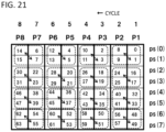
- the first data rearrangement part (first data rearrangement means) 201 rearranges data in a “sequential order” shown in FIG. 20 into data in an “intermediate order” shown in FIG. 21 as the first step rearrangement.
- the “intermediate order” illustrated in FIG. 21 is an order after performing rearrangement as indicated by arrows on data sets each constituted by four pieces of data indicated by a dotted line, in the “sequential order” illustrated in FIG. 20 .
- the “intermediate order” illustrated in FIG. 21 is achieved by exchanging positions of the following data sets in the sequential order in FIG. 20 .
- the second data rearrangement part (second data rearrangement means) 204 performs rearrangement processing from the “intermediate order” illustrated in FIG. 21 into the “bit reverse order” illustrated in FIG. 16 while staying in the sign magnitude—representation.
- this is an order after performing internal rearrangement within each data set as indicated by arrows for each data set constituted by four pieces of data indicated by a dotted line.
- the first data rearrangement part (first data rearrangement means) 201 includes a first data distribution part (first data distribution means) 202 , four RAM circuits 210 a , 210 b , 210 c , and 210 d , and a second data distribution part (second data distribution means) 203 .
- the first data distribution part 202 simultaneously receives eight pieces of data from eight inputs in 0 to in 7 , performs data distribution processing, and outputs the results to eight outputs 205 a to 205 h.
- the RAM circuit 210 a stores two pieces of the data as a set, outputted to 205 a and 205 b by the first data distribution part 202 , and outputs them also as two pieces of data to 206 a and 206 b.
- the RAM circuit 210 b stores two pieces of the data as a set, outputted to 205 c and 205 d by the first data distribution part 202 , and outputs them also as two pieces of data to 206 c and 206 d.
- the RAM circuit 210 c stores two pieces of the data as a set, outputted to 205 e and 205 f by the first data distribution part 202 , and outputs them also as two pieces of data to 206 e and 206 f.
- the RAM circuit 210 d stores two pieces of the data as a set, outputted to 205 g and 205 h by the first data distribution part 202 , and outputs them also as two pieces of data to 206 g and 206 h.
- the second data distribution part 203 simultaneously receives eight pieces of data from eight inputs 206 a to 206 h , performs data distribution processing, and outputs the results to eight outputs 207 a to 207 h.
- the second data rearrangement part (second data rearrangement means) 204 is constituted by four intra-data set rearrangement part 220 a to 220 d.
- the intra-data set rearrangement part 220 a receives two inputs 207 a and 207 b , performs reordering processing inside a data set constituted by four pieces of data, and outputs the result to outputs out 0 and out 1 .
- the intra-data set rearrangement part 220 b receives two inputs 207 c and 207 d , performs reordering processing inside a data set constituted by four pieces of data, and outputs the result to outputs out 2 and out 3 .
- the intra-data set rearrangement part 220 c receives two inputs 207 e and 207 f , performs reordering processing inside a data set constituted by four pieces of data, and outputs the result to outputs out 4 and out 5 .
- the intra-data set rearrangement part 220 d receives two inputs 207 g and 207 h , performs reordering processing inside a data set constituted by four pieces of data, and outputs the result to outputs out 6 and out 7 .
- the data reordering part 200 of FIG. 19 configures the data reordering part 200 of the second data reordering processing part 260 of FIG. 18
- the outputs out 0 to out 7 of the second data rearrangement part (second data rearrangement means) 204 of FIG. 19 correspond to the outputs out 0 to out 7 of the second data reordering processing part 260 of FIG. 18 .
- FIG. 22 is a time chart for illustrating the operation of the data reordering part 200 .
- the horizontal axis in FIG. 22 represents time (denoted by cycle numbers), and each row represents the data in the data line (input/output) of each part in FIG. 19 .
- element numbers 0 to 63 in arrays of the cycles (columns) and the data lines (rows) denote data x( 0 ), . . . , x( 63 ) (for example each data in the data sets P 1 , . . . , P 8 in FIG. 15 ).
- the data reordering part 200 receives 64 pieces of data 0 to 63 in 8-data parallel in the sequential order in eight cycles t 0 to t 7 , and outputs 64 pieces of data 0 to 63 in 8-data parallel in the bit reverse order in eight cycles t 8 to t 15 .
- the first data rearrangement part 201 receives 64 pieces of data 0 to 63 in 8-data parallel in the sequential order in eight cycles t 0 to t 7 , and outputs 64 pieces of data 0 to 63 in 8-data parallel in an intermediate order in eight cycles t 8 to t 15 .
- the first data distribution part 202 performs the following operation. Note that the first data distribution part 202 which is a subject of each operation is omitted.
- the first data distribution part 202 performs the following operation in the cycles t 0 to t 7 .
- the sets of eight pieces of data 0 to 7, 8 to 15, 16 to 23, 24 to 31, 32 to 39, 40 to 47, 48 to 55, and 56 to 63 in (1) to (8) above correspond to x( 0 ) to x( 7 ) constituting the data set P 1 , x( 8 ) to x( 15 ) constituting the data set P 2 , x( 16 ) to x( 23 ) constituting the data set P 3 , x( 24 ) to x( 31 ) constituting the data set P 4 , x( 32 ) to x( 39 ) constituting the data set P 5 , x( 40 ) to x( 47 ) constituting the data set P 6 , x( 48 ) to x( 55 ) constituting the data set P 7 , and x( 56 ) to x( 63 ) constituting the data set P 8 in FIG. 15 , respectively, for example.
- the number n in the data represents the index n of x(
- the first data distribution part 202 performs rotation (rotate) processing on eight pieces of data simultaneously received in parallel and outputs the results, and may be easily realized by, for example, a shift circuit.
- a shift circuit For example, in a register that stores and holds eight pieces of data from in 0 to in 7 in parallel, eight pieces of data from in 6 , in 7 , and in 0 to in 5 in this order can be obtained by rotating right by two pieces of data in, for example, the cycles t 2 and t 3 . Eight pieces of data from in 4 to in 7 and in 0 to in 3 in this order can be obtained by rotating left or right by, for example, four pieces of data in the cycles t 4 and t 5 .
- the RAM circuit 210 a performs the following operation. Note that the outputs 205 a and 205 b of the first data distribution part 202 are referred to as inputs 205 a and 205 b in the description of the RAM circuit 210 a since they are respectively connected to an input of the RAM circuit 210 a .
- the RAM circuit 210 a which is a subject of the following operation is omitted. The same applies to inputs of the RAM circuits 210 b to 210 d.
- the RAM circuit 210 b performs the following operation.
- the RAM circuit 210 c performs the following operation.
- the RAM circuit 210 d performs the following operation.
- the second data distribution part 203 performs the following operation. Note that the outputs 206 a to 206 h of the RAM circuits 210 a to 210 d are referred to as inputs 206 a to 206 h in the description of the second data distribution part 203 since they are connected to the inputs of the second data distribution part 203 .
- the second data distribution part 203 which is a subject of the following operation is omitted.
- the second data distribution part 203 performs the following operation.
- the second data distribution part 203 also performs rotation processing on eight pieces of data simultaneously received in parallel and outputs the results, and may be easily realized by, for example, a shift circuit.
- the second data rearrangement part 204 receives 64 pieces of data 0 to 63 in 8-data parallel in the intermediate order in eight cycles 18 to 115 , and outputs 64 pieces of data 0 to 63 in 8-data parallel in the bit reverse order in eight cycles t 9 to t 16 .
- the intra-data set rearrangement part 220 a performs the following operation.
- the intra-data set rearrangement part 220 a which is a subject of the following operation is omitted.
- the intra-data set rearrangement part 220 b performs the following operation.
- the intra-data set rearrangement part 220 b which is a subject of the following operation is omitted.
- the intra-data set rearrangement part 220 c performs the following operation.
- the intra-data set rearrangement part 220 c which is a subject of the following operation is omitted.
- the intra-data set rearrangement part 220 d performs the following operation.
- the intra-data set rearrangement part 220 d which is a subject of the following operation is omitted.
- the data reordering part 200 achieves rearrangement from the sequential order to the bit reverse order by performing rearrangement from the sequential order to the intermediate order with the first data rearrangement part 201 and performing rearrangement from the intermediate order to the bit reverse order with the second data rearrangement part 204 .
- the intra-data set rearrangement parts 220 a to 220 d constituting the second data rearrangement part 204 may be realized by an intra-data set rearrangement part 220 illustrated in FIG. 23 .
- the intra-data set rearrangement part 220 is constituted by selector circuits 221 , 224 , and 225 , and flip-flops 222 and 223 .
- FIG. 24 is a time chart which shows the operation of the intra-data set rearrangement part 220 .
- the intra-data set rearrangement part 220 receives four pieces of data 0, 1, 8, and 9 as a data set from inputs in 0 and in 1 in cycles t 0 and t 1 , performs rearrangement processing on the pieces within the data set, and outputs four pieces of data 0, 8, 1, and 9 from outputs out 0 and out 1 in the cycle t 1 and cycle t 2 . More specifically, the intra-data set rearrangement part 220 receives 0 and 1 from the inputs in 0 and in 1 in the cycle t 0 , and the selector 221 selects 0 received from the input MO. In the cycle t 0 , the flip-flop 222 stores 0 selected by the selector 221 and the flip-flop 223 stores 1 received from the input in 1 .
- the selector 221 selects 9 received from the input in 1 .
- the flip-flop 222 outputs 0 stored therein and stores 9 received from the input in 1
- the flip-flop 223 outputs 1 stored therein.
- the selector 224 selects 0 outputted by the flip-flop 222 and outputs it to the output out 0
- the selector 225 selects 8 received from the input in 0 and outputs it to the output out 1 .
- the flip-flop 222 outputs 9 stored therein, and the flip-flop 223 outputs 1 stored therein.
- the selector 224 selects 1 outputted by the flip-flop 223 and outputs it to the output out 0
- the selector 225 selects 9 outputted by the flip-flop 222 and outputs it to the output out 1 .
- rearrangement from the bit reverse order to the sequential order may also be achieved in two steps by performing rearrangement from the bit reverse order to the intermediate order as the first-step rearrangement, and then by performing rearrangement from the intermediate order into the sequential order as the second-step rearrangement.
- FIG. 25 illustrates an example of a configuration of a twiddle factor multiplication processing part 270 .
- the twiddle factor multiplication processing part 270 includes compensation circuits 20 a to 20 d , multiplication circuits 271 a to 271 d , conversion circuits 10 a to 10 d , and addition circuits 272 a to 272 b.
- the compensation circuits 20 a to 20 d can be realized by the compensation circuit 20 shown in FIG. 8 , for example.
- the multiplication circuits 271 a to 271 d can be realized, for example, by performing unsigned multiplication processing with the unsigned operation circuit 43 in the operation circuit 41 shown in FIG. 9 .
- the multiplication circuit 271 a performs multiplication processing on the real component B of the input A represented in a sign magnitude—representation and the real component X of the input W represented in a sign magnitude—representation, and outputs the result BX.
- the multiplication circuit 271 b performs multiplication processing on the imaginary component iC of the input A represented in a sign magnitude—representation and the imaginary component iY of the input W represented in a sign magnitude—representation, and outputs the result ⁇ CY.
- the multiplication circuit 271 c performs multiplication processing on the imaginary component iC of the input A represented in a sign magnitude—representation and the real component X of the input W represented in a sign magnitude—representation, and outputs the result iCX.
- the multiplication circuit 271 d performs multiplication processing on the real component B of the input A represented in a sign magnitude—representation and the imaginary component iY of the input W represented in a sign magnitude—representation, and outputs the result BY.
- the conversion circuits 10 a to 10 d can be realized by the conversion circuit 10 shown in FIG. 4 , for example.
- the conversion circuit 10 a converts the signal BX represented in a sign magnitude—representation outputted by the multiplication circuit 271 a to a two's complement representation and outputs the result.
- the conversion circuit 10 b converts the signal ⁇ CY represented in a sign magnitude—representation outputted by the multiplication circuit 271 b to a two's complement representation and outputs the result.
- the conversion circuit 10 c converts the signal iCX represented in a sign magnitude—representation outputted by the multiplication circuit 271 c to a two's complement representation and outputs the result.
- the conversion circuit 10 d converts the signal iBY represented in a sign magnitude—representation outputted by the multiplication circuit 271 d to a two's complement representation and outputs the result.
- the addition circuits 272 a and 272 b are achieved by an addition circuit that performs addition processing on inputs represented in a two's complement representation.
- the addition circuit 272 a performs addition processing on the signal BX represented in the two's complement representation outputted by the conversion circuit 10 a and the signal ⁇ CY represented in the two's complement representation outputted by the conversion circuit 10 b and outputs the result BX ⁇ CY.
- the addition circuit 272 b performs addition processing on the signal iCX represented in the two's complement representation outputted by the conversion circuit 10 c and the signal iBY represented in the two-s complement representation outputted by the conversion circuit 10 d and outputs the result i(CX+BY).
- the FFT apparatus 400 achieves rearrangement from the “sequential order” to the “bit reverse order” and rearrangement from the “bit reverse order” to the “sequential order,” which are data reordering processing required in a butterfly operation, in two steps through the “intermediate order” after conversion into the sign magnitude—representation.
- the percentage-activity of the RAM circuits constituting the first data rearrangement part 201 and the second data rearrangement part 204 , the flip-flop circuits, and the selector circuits can be reduced, compared with a case where the reordering processing is performed while remaining in the two's complement representation.
- the FFT apparatus 400 processes the multiplication processing, among the multiplication processing and the addition processing that constitute the twiddle factor multiplication processing, while remaining in a sign magnitude—representation. Therefore, the percentage-activity can be reduced as compared with the case where the multiplication process is performed in a two's complement representation.
- the conversion processing between the two's complement representation and the sign magnitude—representation can be achieved only with bit inversion processing, and one-addition processing (increment processing), which is necessary in a conventional sign magnitude representation, is not required.
- bit inversion processing can be achieved only with an XOR circuit(s), it can be achieved with an overwhelmingly small circuit scale, compared with other logic processing circuits and operation processing circuits.
- compensation processing for a value of a sign magnitude—representation it is possible to reduce an operation error that occurs even if the operation processing such as multiplication or division is operated while remaining in the sign magnitude—representation, and the number of bits to be compensated can be set to an optimum value according to the allowable operation error. As a result, the circuit scale related to the compensation processing can be reduced.
- the percentage-activity in the data reordering processing can be reduced. Thereby it is possible to reduce the power consumption in the data reordering processing part.
- the butterfly operation processing is processed in butterfly operation processing part while remaining in a two's complement representation. Therefore, although the percentage-activity related to these operation processes is not reduced, the conversion between the data representation formats does not largely increase the circuit scale unlike the case where the sign magnitude representation is applied. Therefore, the power consumption of the entire FFT apparatus can be reduced by the amount that the power consumption related to the data reordering processing and the twiddle factor multiplication processing is reduced.
- FIG. 30 is a diagram schematically illustrating a mode in which a program realizes the processing and functions of the apparatuses 100 and 400 according to the above first and the second example embodiments.
- a processor apparatus 300 comprises a processor 301 , a program storage part 302 that stores a program (instructions, data, etc.) executed by the processor 301 , a RAM 303 (that may function as the RAM circuit 210 of the second example embodiment illustrated in FIG.
- the processor 301 may be a digital signal processor, or the like.
- the program storage part 302 may be a ROM (Read-Only Memory), EEPROM (Electrically Erasable Programmable Read-Only Memory), HDD (Hard Disk Drive), or USB (Universal Serial Bus) memory, etc.
- the program storage part 302 may be configured to store the firmware of the processor 301 .
- the RAM 303 may be configured to be built into the processor 301 .
- the first interface 304 may be configured to comprise an input circuit (or receiving circuit) and an input buffer (receiving buffer) and the second interface 305 may be configured to comprise an output buffer (transmission buffer) and an output circuit (transmission circuit).
- the first and the second interfaces 304 and 305 may be integrated into a single interface circuit comprising an input/output circuit (transceiver).
- the same effects as those of the first and the second example embodiments can be obtained by causing the processor 301 to execute the program stored in the program storage part 302 .
- FIG. 30 illustrates the configuration of the processor apparatus 300 with the parts 301 to 305 merely for the sake of description, however, it goes without saying that some or all of these parts may be included in the processor 301 to form a single chip.
- Patent Literatures 1 to 3 and Non-Patent Literatures 1 and 2 cited above is incorporated herein in its entirety by reference thereto. It is to be noted that it is possible to modify or adjust the example embodiments or examples within the whole disclosure of the present invention (including the Claims) and based on the basic technical concept thereof. Further, it is possible to variously combine or select a wide variety of the disclosed elements (including the individual elements of the individual claims, the individual elements of the individual examples and the individual elements of the individual figures) within the scope of the Claims of the present invention, That is, it is self-explanatory that the present invention includes any types of variations and modifications to be done by a skilled person according to the whole disclosure including the Claims, and the technical concept of the present invention.
- a signal processing apparatus comprising:
Landscapes
- Physics & Mathematics (AREA)
- Engineering & Computer Science (AREA)
- General Physics & Mathematics (AREA)
- Mathematical Physics (AREA)
- Theoretical Computer Science (AREA)
- Computational Mathematics (AREA)
- Mathematical Analysis (AREA)
- Pure & Applied Mathematics (AREA)
- Mathematical Optimization (AREA)
- Data Mining & Analysis (AREA)
- General Engineering & Computer Science (AREA)
- Discrete Mathematics (AREA)
- Algebra (AREA)
- Databases & Information Systems (AREA)
- Software Systems (AREA)
- Computing Systems (AREA)
- Complex Calculations (AREA)
- Human Computer Interaction (AREA)
Abstract
Description
-
- at the first time, the processing corresponding to the
partial data flow 505 a is performed, - at the second time, the processing corresponding to the
partial data flow 505 b is performed, - at the third time, the processing corresponding to the partial data flow 505 c (not shown in the drawing) is performed.
- at the first time, the processing corresponding to the
-
- PTL1: Japanese Unexamined Patent Application Publication No. JP-H08-137832A (pp. 3-5, FIG. 25)
- PTL2: Japanese Unexamined Patent Application Publication No. JP2001-56806A (
Page 5, FIG. 1) - PTL3: Japanese Unexamined Patent Application Publication No. JP2012-22500A (
Page 5, FIG. 1) - NPL1: J. W. Cooley, J. W. Tukey, “An Algorithm for the Machine Calculation of Complex Fourier Series,” Mathematics of Computation, US, American Mathematical Society, April 1965, Vol. 19, No. 90, pp. 297-301
- NPL2: D. P. Kolba. “A Prime Factor FFT Algorithm Using High-Speed Convolution,” IEEE Trans. On Acoustics, US, IEEE Signal Processing Society. August 1977, Vol. 29, No. 4, pp. 281-294
P=(½)*a*C*V 2 *f (1)
-
- a: circuit operation rate (percentage-activity),
- C: load capacity,
- V: voltage, and
- f: operating frequency.
The circuit operation rate (percentage-activity) is given by a ratio of an estimated value of the number of switching times to the number of clock cycles during a certain period of time.
-
- outputting a value zero to a
sign bit 48 when both thesign bit 44 and thesign bit 45 have a value zero; - outputting a value one to the
sign bit 48 when any one of thesign bit 44 and thesign bit 45 has a value one: and - outputting a value zero to the
sign bit 48 when both thesign bit 44 and thesign bit 45 have a value one.
- outputting a value zero to a
ps(i)=x[8×(s−1)+i]
qs(i)=x[(s−1)+8×i]
Qs(i)=Pi+1(s−1)
-
- swapping between 1 and 8 in a data set constituted by {0, 1, 8, 9},
- swapping between 3 and 10 in the data set constituted by {2, 3, 10, 11},
- swapping between 5 and 12 in the data set constituted by {4, 5, 12, 13},
- swapping between 7 and 14 in the data set constituted by {6, 7, 14, 15,}
- swapping between 17 and 24 in the data set constituted by {16, 17, 24, 25},
- swapping between 19 and 26 in a data set constituted by {18, 19, 26, 27},
- swapping between 21 and 28 in the data set constituted by {20, 21, 28, 29},
- swapping between 23 and 30 in the data set constituted by {22, 23, 30, 31},
- swapping between 33 and 40 in the data set constituted by {32, 33, 40, 41},
- swapping between 35 and 42 in the data set constituted by {34, 35, 42, 43},
- swapping between 37 and 44 in a data set constituted by {36, 37, 44, 45},
- swapping between 39 and 46 in the data set constituted by {38, 39, 46, 47},
- swapping between 49 and 56 in the data set constituted by {48, 49, 56, 57},
- swapping between 51 and 58 in the data set constituted by {50, 51, 58, 59},
- swapping between 53 and 60 in the data set constituted by {52, 53, 60, 61}, and
- swapping between 55 and 62 in a data set constituted by {54, 55, 62, 63}.
-
- outputs the data received from in0 to 205 a,
- outputs the data received from in1 to 205 b,
- outputs the data received from in2 to 205 c,
- outputs the data received from in3 to 205 d,
- outputs the data received from in4 to 205 e,
- outputs the data received from in5 to 205 f,
- outputs the data received from in6 to 205 g, and
- outputs the data received from in7 to 205 h.
-
- outputs the data received from in0 to 205 c,
- outputs the data received from in1 to 205 d,
- outputs the data received from in2 to 205 e,
- outputs the data received from in3 to 205 f,
- outputs the data received from in4 to 205 g,
- outputs the data received from in5 to 205 h,
- outputs the data received from in6 to 205 a, and
- outputs the data received from in7 to 205 b.
-
- outputs the data received from in0 to 205 e,
- outputs the data received from in1 to 205 f,
- outputs the data received from in2 to 205 g,
- outputs the data received from in3 to 205 h,
- outputs the data received from in4 to 205 a,
- outputs the data received from in5 to 205 b,
- outputs the data received from in6 to 205 c, and
- outputs the data received from in7 to 205 d.
-
- outputs the data received from in0 to 205 g,
- outputs the data received from in1 to 205 h,
- outputs the data received from in2 to 205 a,
- outputs the data received from in3 to 205 b,
- outputs the data received from in4 to 205 c,
- outputs the data received from in5 to 205 d,
- outputs the data received from in6 to 205 e, and
- outputs the data received from in7 to 205 f.
-
- (1) In the cycle t0, receives eight pieces of
data 0 to 7 from the inputs in0 to in7, respectively, and outputs the eight pieces ofdata 0 to 7 to theoutputs 205 a to 205 h, respectively. - (2) In the cycle t1, receives eight pieces of
data 8 to 15 from the inputs in0 to in7, respectively, and outputs the eight pieces ofdata 8 to 15 to theoutputs 205 a to 205 h, respectively. - (3) In the cycle t2, receives eight pieces of
data 16 to 23 from the inputs in0 to in7, respectively, and outputs the eight pieces of data, 22, 23 and 16 to 21 to theoutputs 205 a to 205 h, respectively. - (4) In the cycle t3, receives eight pieces of
data 24 to 31 from the inputs in0 to in7, respectively, and outputs the eight pieces of data, 30, 31 and 24 to 29 to theoutputs 205 a to 205 h, respectively. - (5) In the cycle t4, receives eight pieces of
data 32 to 39 from the inputs in0 to in7, respectively, and outputs the eight pieces of data, 36 to 39 and 32 to 35 to theoutputs 205 a to 205 h, respectively. - (6) In the cycle t5, receives eight pieces of
data 40 to 47 from the inputs in0 to in7, respectively, and outputs the eight pieces of data, 44 to 47 and 40 to 43 to theoutputs 205 a to 205 h, respectively. - (7) In the cycle t6, receives eight pieces of
data 48 to 55 from the inputs in0 to in7, respectively, and outputs the eight pieces of data, 50 to 55, 48 and 49 to theoutputs 205 a to 205 h, respectively. - (8) In the cycle t7, receives eight pieces of
data 56 to 63 from the inputs in0 to in7, respectively, and outputs the eight pieces of data, 58 to 63, 56 and 57 to theoutputs 205 a to 205 h, respectively.
- (1) In the cycle t0, receives eight pieces of
-
- (1) Outputs received
data inputs outputs - (2) Outputs received
data inputs outputs - (3) Outputs received
data inputs outputs - (4) Outputs received
data inputs outputs - (5) Outputs received
data inputs outputs - (6) Outputs received
data inputs outputs - (7) Outputs received
data inputs outputs - (8) Outputs received
data inputs outputs
- (1) Outputs received
-
- (1) Outputs received two pieces of
data inputs outputs - (2) Outputs received two pieces of
data inputs outputs - (3) Outputs received two pieces of
data inputs outputs - (4) Outputs received two pieces of
data inputs outputs - (5) Outputs received two pieces of
data inputs outputs - (6) Outputs received two pieces of
data inputs outputs - (7) Outputs received two pieces of
data inputs outputs - (8) Outputs received two pieces of
data inputs outputs
- (1) Outputs received two pieces of
-
- outputs the data received from 206 a to 207 a,
- outputs the data received from 206 b to 207 b,
- outputs the data received from 206 c to 207 c,
- outputs the data received from 206 d to 207 d,
- outputs the data received from 206 e to 207 e,
- outputs the data received from 206 f to 207 f,
- outputs the data received from 206 g to 207 g, and
- outputs the data received from 206 h to 207 h.
-
- outputs the data received from 206 a to 207 g,
- outputs the data received from 206 b to 207 h,
- outputs the data received from 206 c to 207 a,
- outputs the data received from 206 d to 207 b,
- outputs the data received from 206 e to 207 c,
- outputs the data received from 206 f to 207 d,
- outputs the data received from 206 g to 207 e, and
- outputs the data received from 206 h to 207 f.
-
- outputs the data received from 206 a to 207 e,
- outputs the data received from 206 b to 207 f,
- outputs the data received from 206 c to 207 g,
- outputs the data received from 206 d to 207 h,
- outputs the data received from 206 e to 207 a,
- outputs the data received from 206 f to 207 b,
- outputs the data received from 206 g to 207 c, and
- outputs the data received from 206 h to 207 d.
-
- outputs the data received from 206 a to 207 c,
- outputs the data received from 206 b to 207 d,
- outputs the data received from 206 c to 207 e,
- outputs the data received from 206 d to 207 f,
- outputs the data received from 206 e to 207 g,
- outputs the data received from 206 f to 207 h,
- outputs the data received from 206 g to 207 a, and
- outputs the data received from 206 h to 207 b.
-
- (1) In the cycle t8, receives eight pieces of
data inputs 206 a to 206 h, respectively, and outputs the eight pieces ofdata outputs 207 a to 207 h, respectively. - (2) In the cycle t9, receives eight pieces of
data inputs 206 a to 206 h, respectively, and outputs the eight pieces ofdata outputs 207 a to 207 h, respectively. - (3) In the cycle t10, receives eight pieces of
data inputs 206 a to 206 h, respectively, and outputs the eight pieces ofdata outputs 207 a to 207 h, respectively. - (4) In the cycle t11, receives eight pieces of
data inputs 206 a to 206 h, respectively, and outputs the eight pieces ofdata outputs 207 a to 207 h, respectively. - (5) In the cycle t12, receives eight pieces of
data inputs 206 a to 206 h, respectively, and outputs the eight pieces ofdata outputs 207 a to 207 h, respectively. - (6) In the cycle t13, receives eight pieces of
data inputs 206 a to 206 h, respectively, and outputs the eight pieces ofdata outputs 207 a to 207 h, respectively. - (7) In the cycle t14, receives eight pieces of
data inputs 206 a to 206 h, respectively, and outputs the eight pieces ofdata outputs 207 a to 207 h, respectively. - (8) In the cycle t15, receives eight pieces of
data inputs 206 a to 206 h, respectively, and outputs the eight pieces ofdata outputs 207 a to 207 h, respectively.
- (1) In the cycle t8, receives eight pieces of
-
- receives two pieces of
data - receives two pieces of
data - to the outputs out0 and out1,
- outputs two piece of
data - outputs two pieces of
data
- receives two pieces of
-
- receives two pieces of
data - receives two pieces of
data - to the outputs out0 and out1,
- outputs two piece of
data - outputs two pieces of
data
- receives two pieces of
-
- receives two pieces of
data - receives two pieces of
data - to the outputs out0 and out1,
- outputs two piece of
data - outputs two pieces of
data
- receives two pieces of
-
- receives two pieces of
data - receives two pieces of
data - to the outputs out0 and out1,
- outputs two piece of
data - outputs two pieces of
data
- receives two pieces of
-
- receives two pieces of
data - receives two pieces of
data - to the outputs out2 and out3,
- outputs two piece of
data - outputs two pieces of
data
- receives two pieces of
-
- from the
inputs - receives two pieces of
data - receives two pieces of
data - to the outputs out2 and out3,
- outputs two piece of
data - outputs two pieces of
data
- from the
-
- receives two pieces of
data - receives two pieces of
data - to the outputs out2 and out3,
- outputs two piece of
data - outputs two pieces of
data
- receives two pieces of
-
- receives two pieces of
data - receives two pieces of
data - to the outputs out2 and out3,
- outputs two piece of
data - outputs two pieces of
data
- receives two pieces of
-
- receives two pieces of
data - receives two pieces of
data - to the outputs out4 and out5,
- outputs two piece of
data - outputs two pieces of
data
- receives two pieces of
-
- from the
inputs - receives two pieces of
data - receives two pieces of
data - to the outputs out4 and out5,
- outputs two piece of
data - outputs two pieces of
data
- from the
-
- receives two pieces of
data - receives two pieces of
data - to the outputs out4 and out5,
- outputs two piece of
data - outputs two pieces of
data
- receives two pieces of
-
- receives two pieces of
data - receives two pieces of
data - to the outputs out4 and out5,
- outputs two piece of
data - outputs two pieces of
data
- receives two pieces of
-
- receives two pieces of
data - receives two pieces of
data - to the outputs out6 and out7,
- outputs two piece of
data - outputs two pieces of
data
- receives two pieces of
-
- receives two pieces of
data - receives two pieces of
data - to the outputs out6 and out7,
- outputs two piece of
data - outputs two pieces of
data
- receives two pieces of
-
- receives two pieces of
data - receives two pieces of
data - to the outputs out6 and out7,
- outputs two piece of
data - outputs two pieces of
data
- receives two pieces of
-
- receives two pieces of
data - receives two pieces of
data - to the outputs out6 and out7,
- outputs two pieces of
data - outputs two pieces of
data
- receives two pieces of
A=B+iC and
W=X+iY
(where i2=−1), and calculates and outputs a result of complex multiplication
T=A×W=(BX−CY)+i(CX+BY).
T=A×W(BX−CY)+i(CX+BY).
-
- a storage processing part that performs storage processing on data represented in a second representation format, wherein, when a value of the data is positive or zero, the second representation format is identical to a representation format of two's complement, while, when the value of the data is negative, the second representation format is a representation format in which all bits other than a most significant bit indicating a sign in a two's complement representation of the data are inverted; and
- an operation processing part that performs operation processing on at least one of data represented in the two's complement representation or data obtained by applying compensation processing to data represented in the second representation format.
[Note 2]
The signal processing apparatus according tonote 1, wherein the compensation processing adds a value one to M bits from a least significant bit (where M is a positive integer and not more than N) in data of N bits (where N is a predetermined positive integer) when the data of N bits (N being a positive integer) represented in the second representation format has a negative value.
[Note 3]
The signal processing apparatus according tonote
[Note 4]
The signal processing apparatus according to any one ofnotes 1 to 3, wherein the storage processing part comprises:
at least one selected from: - a configuration including a storage circuit; and
- a configuration including a storage circuit and at least one of a first conversion part or a second conversion part,
- wherein the first conversion part receives data represented in a two's complement representation to convert the received data from the two's complement representation to the second representation format,
- wherein the storage circuit performs storage processing of and outputs the data in the second representation format, and
- wherein the second conversion part receives the data represented in the second representation format outputted from the storage circuit to convert the received data into a two's complement representation for output.
[Note 5]
The signal processing apparatus according to any one ofnotes 1 to 3, wherein the operation processing part comprises:
at least one selected from: - a configuration including a first operation circuit;
- a configuration including a compensation circuit and a second operation circuit; and
- a configuration including a compensation circuit and a second operation circuit and further comprising at least one of a first conversion part or a second conversion part,
- wherein the first operation circuit receives data represented in a two's complement representation and performs operation processing on the data represented in the two's complement representation,
- wherein the first conversion part receives data represented in a two's complement representation to convert the received data from the two's complement representation to the second representation format,
- wherein the compensation circuit performs the compensation processing on data represented in the second representation format,
- wherein the second operation circuit receives data having the compensation processing applied thereto by the compensation circuit and performs operation processing on the data having the compensation processing applied thereto, and
- wherein the second conversion part receives data represented in the second representation format and converts the received data to a two's complement representation for output.
[Note 6]
The signal processing apparatus according tonote 5, wherein the second operation circuit comprises: - a sign operation circuit that outputs a result of an operation performed on one or more sign bits of one or more individual items of data of operation target in the second representation format with the compensation processing applied thereto, as a sign bit; and
- an unsigned operation circuit that performs an operation on one or more magnitude parts other than the one or more sign bits of the one or more individual items of data of operation target represented in the second representation format with the compensation processing applied thereto for output.
[Note 7]
The signal processing apparatus according to any one ofnotes 4 to 6, wherein the first conversion part and the second conversion part each output a most significant bit of the received data as it is, and - as for each bit other than the most significant bit, output a result of taking exclusive OR of the each bit and the most significant bit.
[Note 8]
The signal processing apparatus according tonote - a butterfly operation processing part that performs butterfly operation processing; and
- a twiddle factor multiplication processing part that performs twiddle factor multiplication processing,
- wherein the storage processing part comprises
a data reordering processing part that rearranges an order of a plurality of data, - wherein the butterfly operation processing part performs the butterfly operation processing on data represented in the two's complement representation,
- wherein the twiddle factor multiplication processing part performs operation processing on data obtained by applying compensation processing to data represented in the second representation format, for multiplication processing, and performs operation processing on data represented in a two's complement representation, for addition processing, and
- wherein the data reordering processing part performs storage processing on data represented in the second representation format.
[Note 9]
The signal processing apparatus according tonote 8, wherein the data reordering processing part comprises: - a first conversion part that receives data represented in a two's complement representation and converts it into the second representation format; and
- a second conversion part that receives data represented in the second representation format and converts it into a two's complement representation,
- wherein the first conversion part converts received data represented in a two's complement representation into the second representation format and performs data reordering processing, and
- wherein the second conversion part converts data represented in the second representation format with the data reordering applied into a two's complement representation for output.
[Note 10]
The signal processing apparatus according tonote - as for each bit other than the most significant bit, output a result of taking exclusive OR of the each bit and the most significant bit.
[Note 11]
An FFT apparatus performing a fast Fourier transform (FFT) or an inverse fast Fourier transform (IFFT), comprising: - a butterfly operation processing part that performs butterfly operation processing; and
- a twiddle factor multiplication processing part that performs twiddle factor multiplication processing; and
- a data reordering processing part that rearranges an order of a plurality of data,
- wherein the apparatus performs an operation using both a two's complement representation and a second representation format which is different from the two's complement representation, as a data representation format,
- wherein, when a value of the data is positive or zero, the second representation format is identical to a representation format of two's complement, while, when the value of the data is negative, the second representation format is a representation format in which all bits other than a most significant bit indicating a sign in a two's complement representation of the data are inverted,
- wherein the butterfly operation processing part performs the processing on data represented in a two's complement representation;
- wherein the data reordering processing part performs storage processing on data represented in the second representation format,
- wherein the twiddle factor multiplication processing part performs operation processing on data obtained by applying compensation processing to data represented in the second representation format, for multiplication processing, and performs operation processing on data represented in a two's complement representation, for addition processing.
[Note 12]
The FFT apparatus according to note 11, wherein the compensation processing performs processing in which a value one is added to M bits from a least significant bit (where M is a positive integer and not more than N) in data of N bits (where N is a positive integer) when the data of N bits (N being a positive integer) represented in the second representation format has a negative value.
[Note 13]
The FFT apparatus according to note 11 or 12, wherein the data reordering processing part comprises: - a first conversion part that converts data from a two's complement representation to the second representation format; and
- a second conversion part that converts data from the second representation format to a two's complement representation, wherein the first conversion part converts received data represented in a two's complement representation into a second representation format and performs data reordering processing,
- wherein the second conversion part converts data represented in the second representation format with the data reordering applied into a two's complement representation for output.
[Note 14]
The FFT apparatus according to any one ofnotes 11 to 13, wherein the first conversion part and the second conversion part each output a most significant bit of the received data as it is, and - as for each bit other than the most significant bit, output a result of taking exclusive OR of the each bit and the most significant bit.
[Note 15]
A signal processing method, comprising steps of: - performing storage processing on data represented in a second representation format that is different from a two's complement representation; and
- performing operation processing on at least one of data represented in a two's complement representation or data obtained by applying compensation processing to data represented in the second representation format, wherein, when a value of the data is positive or zero, the second representation format is identical to a representation format of two's complement, while, when the value of the data is negative, the second representation format is a representation format in which all bits other than a most significant bit indicating a sign in a two's complement representation of the data are inverted.
[Note 16]
The signal processing method according to note 15, comprising - in the compensation processing, adding a value one to M bits from a least significant bit (where M is a positive integer and not more than N) in data of N bits (where N is a predetermined positive integer) when the data of N bits (N being a positive integer) represented in the second representation format has a negative value.
[Note 17]
The signal processing method according to note 15 or 16, comprising: - in the operation processing, performing the operation processing on any of data obtained by applying the compensation processing to data represented in the second representation format when an operation to be processed is a multiplication or a division: and
- performing the operation processing on data represented in a two's complement representation when an operation to be processed is an addition or a subtraction.
[Note 18]
The signal processing method according to any one ofnotes 15 to 17, wherein the storage processing comprises at least one of - storage processing, and
- at least one of a first conversion processing or a second conversion processing prior to or behind the storage processing,
- the first conversion processing receiving data represented in a two's complement representation to convert the received data from the two's complement representation to the second representation format, the storage processing storing the data in the second representation format into the storage circuit,
- the second conversion processing receiving the data represented in the second representation format outputted from the storage circuit to convert the received data into a two's complement representation for output.
[Note 19]
The signal processing method according to any one ofnotes 15 to 17, wherein the operation processing comprises: - at least one selected from:
- first operation processing;
- compensation processing and a second operation processing; and
- compensation processing, second operation processing, and further at least one of first conversion processing or second conversion processing,
- wherein the first operation processing receives data represented in a two's complement representation to perform operation processing on the data represented in the two's complement representation,
- wherein the first conversion processing receiving data represented in a two's complement representation to convert the received data from the two's complement representation to the second representation format,
- wherein the compensation processing performs the compensation processing on data represented in the second representation format,
- wherein the second operation processing performs operation processing on the data having the compensation processing applied thereto, and
- wherein the second conversion processing receives data represented in the second representation format to convert the received data to a two's complement representation for output.
[Note 20]
The signal processing method according to note 15 or 16, comprising
- performing a fast Fourier transform or an inverse fast Fourier transform using both a two's complement representation and the second representation format as data representation format, wherein the operation processing comprises:
- butterfly operation processing performing butterfly operation processing; and
- twiddle factor multiplication processing performing twiddle factor multiplication processing, to perform a fast Fourier transform or an inverse fast Fourier transform,
- wherein the storage processing comprises
- data reordering processing rearranging an order of a plurality of data,
- wherein the butterfly operation processing performs the butterfly operation processing on data represented in the two's complement representation,
- wherein the twiddle factor multiplication processing performs operation processing on data obtained by applying compensation processing to data represented in the second representation format, for multiplication processing, and performs operation processing on data represented in a two's complement representation, for addition processing, and
- wherein the data reordering processing performs storage processing on data represented in the second representation format.
[Note 21]
The signal processing method according to note 20, wherein the data reordering processing comprises: - a first conversion processing converting data from a two's complement representation into the second representation format; and
- a second conversion processing converting from the second representation format into a two's complement representation,
- wherein the first conversion processing converts received data represented in a two's complement representation into the second representation format and performs data reordering processing, and
- wherein the second conversion processing converts data represented in the second representation format with the data reordering applied into a two's complement representation for output.
[Note 22]
An FFT operation method for performing a fast Fourier transform (FFT) or an inverse fast Fourier transform (IFFT) comprising - butterfly operation processing performing butterfly operation processing;
- twiddle factor multiplication processing performing twiddle factor multiplication processing; and
- data reordering processing rearranging an order of a plurality of data, the method comprising:
- performing an operation using both a two's complement representation and the second representation format that is different from the two's complement representation as data representation format, wherein, when a value of the data is positive or zero, the second representation format is identical to a representation format of two's complement, while, when the value of the data is negative, the second representation format is a representation format in which all bits other than a most significant bit indicating a sign in a two's complement representation of the data are inverted,
- wherein the butterfly operation processing performs the processing on data represented in the two's complement representation,
- wherein the data reordering processing performs storage processing on data represented in the second representation format.
- wherein the twiddle factor multiplication processing performs operation processing on data obtained by applying compensation processing to data represented in the second representation format, for multiplication processing, and performs operation processing on data represented in a two's complement representation, for addition processing.
[Note 23]
The FFT operation method according to note 22, comprising - the compensation processing adding a value one to NM bits from a least significant bit (where M is a positive integer and not more than N) in data of N bits (where N is a positive integer) when the data of N bits (N being a positive integer) represented in the second representation format has a negative value.
[Note 24]
The FFT operation method according to note 22 or 23, wherein - the data reordering processing comprises:
- first conversion processing converting data from a two's complement representation to the second representation format; and
- second conversion processing converting from the second representation format to a two's complement representation,
- wherein the first conversion processing converts received data represented in a two's complement representation into a second representation format and performs data reordering processing, and
- wherein the second conversion processing converts data subjected to the data reordering processing on data represented in the second representation format into a two's complement representation for output.
[Note 25]
A program causing a computer to execute:
- a storage processing on data represented in a second representation format, wherein, when a value of the data is positive or zero, the second representation format is identical to a representation format of two's complement, while, when the value of the data is negative, the second representation format is a representation format in which all bits other than a most significant bit indicating a sign in a two's complement representation of the data are inverted; and
- an operation processing on at least any one of data represented in the two's complement representation or data obtained by applying compensation processing to data represented in the second representation format.
[Note 26]
The program according to note 25, wherein the compensation processing adds a value one to M bits from a least significant bit (where M is a positive integer and not more than N) in data of N bits (where N is a predetermined positive integer) when the data of N bits (N being a positive integer) represented in the second representation format has a negative value.
[Note 27]
The program according to note 25 or 26, comprising: - performing the operation processing on any of data obtained by applying the compensation processing to data represented in the second representation format when an operation to be processed is a multiplication or a division; and
- performing the operation processing on data represented in a two's complement representation when an operation to be processed is an addition or a subtraction.
[Note 28]
The program according to any one ofnotes 25 to 27, wherein the storage processing comprises at least one of: - storage processing, and
- at least one of a first conversion processing or a second conversion processing prior to or behind the storage processing,
- wherein the first conversion processing receives data represented in a two's complement representation to convert the received data from wherein the two's complement representation to the second representation format,
- wherein the storage processing stores the data represented in the second representation format into the storage circuit, and
- wherein the second conversion processing receives the data represented in the second representation format outputted from the storage circuit to convert the received data into a two's complement representation for output.
[Note 29]
The program according to any one ofnotes 25 to 27, wherein - the operation processing comprises:
- at least one selected from:
- first operation processing;
- compensation processing and second operation processing; and compensation processing and second operation processing, and further at least one of first conversion processing or second conversion processing,
- wherein the first operation processing receives data represented in a two's complement representation to perform operation processing on the data represented in the two's complement representation,
- wherein the first conversion processing receives data represented in a two's complement representation to convert the received data from the two's complement representation to the second representation format,
- wherein the compensation processing performs the compensation processing on data represented in the second representation format,
- wherein the second operation processing performs operation processing on the data having the compensation processing applied thereto, and
- wherein the second conversion processing receives data represented in the second representation format and converts the received data to a two's complement representation for output.
[Note 30]
The program according to note 25 or 26, wherein the operation processing comprises:
- butterfly operation processing that performs butterfly operation processing; and
- twiddle factor multiplication processing that performs twiddle factor multiplication processing to perform a fast Fourier transform or an inverse fast Fourier transform,
- wherein the storage processing comprises data reordering processing that rearranges an order of a plurality of data,
- wherein the butterfly operation processing performs the butterfly operation processing on data represented in the two's complement representation,
- wherein the twiddle factor multiplication processing performs operation processing on data obtained by applying compensation processing to data represented in the second representation format, for multiplication processing, and performs operation processing on data represented in a two's complement representation, for addition processing, and
- wherein the data reordering processing performs storage processing on data represented in the second representation format.
[Note 31]
-
- a first conversion processing that converts data from a two's complement representation into the second representation format; and
- a second conversion processing that converts from the second representation format into a two's complement representation,
- wherein the first conversion processing converts received data represented in a two's complement representation into a second representation format and performs data reordering processing, and
- wherein the second conversion processing converts data represented in the second representation format with the data reordering applied into a two's complement representation for output.
Claims (10)
Applications Claiming Priority (3)
| Application Number | Priority Date | Filing Date | Title |
|---|---|---|---|
| JP2018-097761 | 2018-05-22 | ||
| JP2018097761 | 2018-05-22 | ||
| PCT/JP2019/020041 WO2019225576A1 (en) | 2018-05-22 | 2019-05-21 | Signal processing device, method and program |
Publications (2)
| Publication Number | Publication Date |
|---|---|
| US20210342102A1 US20210342102A1 (en) | 2021-11-04 |
| US12019700B2 true US12019700B2 (en) | 2024-06-25 |
Family
ID=68616944
Family Applications (1)
| Application Number | Title | Priority Date | Filing Date |
|---|---|---|---|
| US17/057,082 Active 2041-07-20 US12019700B2 (en) | 2018-05-22 | 2019-05-21 | Signal processing apparatus, method, program, and recording medium |
Country Status (3)
| Country | Link |
|---|---|
| US (1) | US12019700B2 (en) |
| JP (1) | JP6977883B2 (en) |
| WO (1) | WO2019225576A1 (en) |
Families Citing this family (2)
| Publication number | Priority date | Publication date | Assignee | Title |
|---|---|---|---|---|
| JP7639461B2 (en) * | 2021-03-29 | 2025-03-05 | 日本電気株式会社 | Fast Fourier transform device and digital filter device |
| CN115833845B (en) * | 2023-01-06 | 2023-05-19 | 北京象帝先计算技术有限公司 | Position output device and position output method |
Citations (19)
| Publication number | Priority date | Publication date | Assignee | Title |
|---|---|---|---|---|
| US4520347A (en) * | 1982-11-22 | 1985-05-28 | Motorola, Inc. | Code conversion circuit |
| US4841467A (en) * | 1987-10-05 | 1989-06-20 | General Electric Company | Architecture to implement floating point multiply/accumulate operations |
| US5148161A (en) * | 1988-04-18 | 1992-09-15 | Fujitsu Ten Limited | Digital signal processor for fixed and floating point data |
| JPH04281518A (en) | 1991-03-11 | 1992-10-07 | Nec Corp | Digital signal processor |
| US5379038A (en) * | 1992-08-06 | 1995-01-03 | Nec Corporation | Parallel-serial data converter |
| JPH08137832A (en) | 1994-11-07 | 1996-05-31 | Fujitsu Ltd | Butterfly arithmetic circuit and fast Fourier transform device using the same circuit |
| JP2001056806A (en) | 1999-06-10 | 2001-02-27 | Matsushita Electric Ind Co Ltd | Fast Fourier transform device |
| JP2001100979A (en) | 1999-07-27 | 2001-04-13 | Denso Corp | Signed integer multiplication method and apparatus |
| JP2001306547A (en) | 2000-04-21 | 2001-11-02 | Sony Corp | Device and method for computation |
| JP2003101415A (en) | 2001-09-19 | 2003-04-04 | Seiko Epson Corp | Data conversion device, data generation device, data conversion program and data generation program, and data conversion method and data generation method |
| JP2003143040A (en) | 2001-11-07 | 2003-05-16 | Sanyo Electric Co Ltd | Digital matched filter and portable wireless terminal employing digital matched filter |
| US20050071403A1 (en) * | 2003-09-29 | 2005-03-31 | Broadcom Corporation | Method, system, and computer program product for executing SIMD instruction for flexible FFT butterfly |
| JP2005184310A (en) | 2003-12-18 | 2005-07-07 | Matsushita Electric Ind Co Ltd | Contour correction device |
| JP2008242594A (en) | 2007-03-26 | 2008-10-09 | Nec Electronics Corp | Filter computing unit and motion compensation device |
| US20100002572A1 (en) * | 2008-07-01 | 2010-01-07 | Broadcom Corporation | Dynamic precision for datapath modules |
| JP2012022500A (en) | 2010-07-14 | 2012-02-02 | Mitsubishi Electric Corp | Fft operation device |
| US20150363360A1 (en) * | 2013-01-23 | 2015-12-17 | Nec Corporation | Fast fourier transform device, fast fourier transform method, and recording medium storing fast fourier transform program |
| US20160140083A1 (en) * | 2013-07-23 | 2016-05-19 | Nec Corporation | Digital filter device, digital filtering method, and storage medium having digital filter program stored thereon |
| US20170083479A1 (en) * | 2015-09-22 | 2017-03-23 | Samsung Electronics Co., Ltd. | Digital signal processor using signed magnitude and wireless communication receiver having the same |
-
2019
- 2019-05-21 JP JP2020521241A patent/JP6977883B2/en active Active
- 2019-05-21 WO PCT/JP2019/020041 patent/WO2019225576A1/en not_active Ceased
- 2019-05-21 US US17/057,082 patent/US12019700B2/en active Active
Patent Citations (19)
| Publication number | Priority date | Publication date | Assignee | Title |
|---|---|---|---|---|
| US4520347A (en) * | 1982-11-22 | 1985-05-28 | Motorola, Inc. | Code conversion circuit |
| US4841467A (en) * | 1987-10-05 | 1989-06-20 | General Electric Company | Architecture to implement floating point multiply/accumulate operations |
| US5148161A (en) * | 1988-04-18 | 1992-09-15 | Fujitsu Ten Limited | Digital signal processor for fixed and floating point data |
| JPH04281518A (en) | 1991-03-11 | 1992-10-07 | Nec Corp | Digital signal processor |
| US5379038A (en) * | 1992-08-06 | 1995-01-03 | Nec Corporation | Parallel-serial data converter |
| JPH08137832A (en) | 1994-11-07 | 1996-05-31 | Fujitsu Ltd | Butterfly arithmetic circuit and fast Fourier transform device using the same circuit |
| JP2001056806A (en) | 1999-06-10 | 2001-02-27 | Matsushita Electric Ind Co Ltd | Fast Fourier transform device |
| JP2001100979A (en) | 1999-07-27 | 2001-04-13 | Denso Corp | Signed integer multiplication method and apparatus |
| JP2001306547A (en) | 2000-04-21 | 2001-11-02 | Sony Corp | Device and method for computation |
| JP2003101415A (en) | 2001-09-19 | 2003-04-04 | Seiko Epson Corp | Data conversion device, data generation device, data conversion program and data generation program, and data conversion method and data generation method |
| JP2003143040A (en) | 2001-11-07 | 2003-05-16 | Sanyo Electric Co Ltd | Digital matched filter and portable wireless terminal employing digital matched filter |
| US20050071403A1 (en) * | 2003-09-29 | 2005-03-31 | Broadcom Corporation | Method, system, and computer program product for executing SIMD instruction for flexible FFT butterfly |
| JP2005184310A (en) | 2003-12-18 | 2005-07-07 | Matsushita Electric Ind Co Ltd | Contour correction device |
| JP2008242594A (en) | 2007-03-26 | 2008-10-09 | Nec Electronics Corp | Filter computing unit and motion compensation device |
| US20100002572A1 (en) * | 2008-07-01 | 2010-01-07 | Broadcom Corporation | Dynamic precision for datapath modules |
| JP2012022500A (en) | 2010-07-14 | 2012-02-02 | Mitsubishi Electric Corp | Fft operation device |
| US20150363360A1 (en) * | 2013-01-23 | 2015-12-17 | Nec Corporation | Fast fourier transform device, fast fourier transform method, and recording medium storing fast fourier transform program |
| US20160140083A1 (en) * | 2013-07-23 | 2016-05-19 | Nec Corporation | Digital filter device, digital filtering method, and storage medium having digital filter program stored thereon |
| US20170083479A1 (en) * | 2015-09-22 | 2017-03-23 | Samsung Electronics Co., Ltd. | Digital signal processor using signed magnitude and wireless communication receiver having the same |
Non-Patent Citations (4)
| Title |
|---|
| D.P. Kolba, "A Prime Factor FFT Algorithm Using High-Speed Convolution," IEEE Trans. On Acoustics, US, IEEE Signal Processing Society, Aug. 1977, vol. 29, No. 4, pp. 281-294, (1977). |
| International Search Report dated Jul. 16, 2019, in corresponding PCT International Application. |
| J.W. Cooley et al., "An Algorithm for the Machine Calculation of Complex Fourier Series," Mathematics of Computation, US, American Mathematical Society, Apr. 1965, vol. 19, No. 90, pp. 297-301, (1965). |
| Masaichi, JP 2003011415 (translation version), Aug. 19, 2001, p. 3-18, figures 1-11 (Year: 2001). * |
Also Published As
| Publication number | Publication date |
|---|---|
| US20210342102A1 (en) | 2021-11-04 |
| WO2019225576A1 (en) | 2019-11-28 |
| JPWO2019225576A1 (en) | 2021-07-01 |
| JP6977883B2 (en) | 2021-12-08 |
Similar Documents
| Publication | Publication Date | Title |
|---|---|---|
| US11604852B2 (en) | Signal processing apparatus, method, program, and recording medium | |
| US9785614B2 (en) | Fast Fourier transform device, fast Fourier transform method, and recording medium storing fast Fourier transform program | |
| US9934199B2 (en) | Digital filter device, digital filtering method, and storage medium having digital filter program stored thereon | |
| US9727531B2 (en) | Fast fourier transform circuit, fast fourier transform processing method, and program recording medium | |
| US12019700B2 (en) | Signal processing apparatus, method, program, and recording medium | |
| US11764942B2 (en) | Hardware architecture for memory organization for fully homomorphic encryption | |
| JP5763911B2 (en) | Radix-8 fixed-point FFT logic circuit characterized by holding root i (√i) operation | |
| JP7848522B2 (en) | Fast Fourier Transform apparatus, digital filter apparatus, fast Fourier transform method, and program | |
| US20240345805A1 (en) | Multi-dimensional fft computation pipelined hardware architecture using radix-3 and radix-2² butterflies | |
| US20260003931A1 (en) | Signal processing apparatus and method | |
| US20250245005A1 (en) | Signal processing apparatus and method | |
| JP6992745B2 (en) | Digital filter device, digital filter processing method and digital filter processing program | |
| JP6436087B2 (en) | Digital filter device, digital filter processing method and program | |
| JP6451647B2 (en) | Fast Fourier transform apparatus, fast Fourier transform method, and fast Fourier transform program | |
| US20200372095A1 (en) | Fast fourier transform device, data sorting processing device, fast fourier transform processing method, and program recording medium | |
| WO2021193947A1 (en) | Digital filter device | |
| JP7639461B2 (en) | Fast Fourier transform device and digital filter device | |
| US12531723B2 (en) | Architecture for number theoretic transform and inverse number theoretic transform | |
| JP4405452B2 (en) | Inverse conversion circuit | |
| WO2021124413A1 (en) | Filter device | |
| US20210182061A1 (en) | Information processing device, information processing method, and program | |
| JP2010072981A (en) | Product-sum operation device and product-sum operation method for complex number | |
| WO2013039458A1 (en) | A system for performing a modular arithmetic operation of input operands |
Legal Events
| Date | Code | Title | Description |
|---|---|---|---|
| AS | Assignment |
Owner name: NEC CORPORATION, JAPAN Free format text: ASSIGNMENT OF ASSIGNORS INTEREST;ASSIGNORS:SHIBAYAMA, ATSUFUMI;YAMAGIWA, HAJIME;SIGNING DATES FROM 20200907 TO 20200922;REEL/FRAME:054429/0779 |
|
| STPP | Information on status: patent application and granting procedure in general |
Free format text: DOCKETED NEW CASE - READY FOR EXAMINATION |
|
| STPP | Information on status: patent application and granting procedure in general |
Free format text: NON FINAL ACTION MAILED |
|
| STPP | Information on status: patent application and granting procedure in general |
Free format text: RESPONSE TO NON-FINAL OFFICE ACTION ENTERED AND FORWARDED TO EXAMINER |
|
| STPP | Information on status: patent application and granting procedure in general |
Free format text: NOTICE OF ALLOWANCE MAILED -- APPLICATION RECEIVED IN OFFICE OF PUBLICATIONS |
|
| ZAAB | Notice of allowance mailed |
Free format text: ORIGINAL CODE: MN/=. |
|
| STPP | Information on status: patent application and granting procedure in general |
Free format text: PUBLICATIONS -- ISSUE FEE PAYMENT VERIFIED |
|
| STCF | Information on status: patent grant |
Free format text: PATENTED CASE |