US11925101B2 - Organic semiconducting compound and the organic photoelectric components using the same - Google Patents
Organic semiconducting compound and the organic photoelectric components using the same Download PDFInfo
- Publication number
- US11925101B2 US11925101B2 US17/930,868 US202217930868A US11925101B2 US 11925101 B2 US11925101 B2 US 11925101B2 US 202217930868 A US202217930868 A US 202217930868A US 11925101 B2 US11925101 B2 US 11925101B2
- Authority
- US
- United States
- Prior art keywords
- group
- substituted
- alkyl
- unsubstituted
- organic
- Prior art date
- Legal status (The legal status is an assumption and is not a legal conclusion. Google has not performed a legal analysis and makes no representation as to the accuracy of the status listed.)
- Active
Links
- 150000001875 compounds Chemical class 0.000 title claims abstract description 117
- 125000000623 heterocyclic group Chemical group 0.000 claims description 60
- WYURNTSHIVDZCO-UHFFFAOYSA-N Tetrahydrofuran Chemical compound C1CCOC1 WYURNTSHIVDZCO-UHFFFAOYSA-N 0.000 claims description 58
- 239000000203 mixture Substances 0.000 claims description 43
- 125000000217 alkyl group Chemical group 0.000 claims description 38
- 125000003118 aryl group Chemical group 0.000 claims description 30
- YLQBMQCUIZJEEH-UHFFFAOYSA-N tetrahydrofuran Natural products C=1C=COC=1 YLQBMQCUIZJEEH-UHFFFAOYSA-N 0.000 claims description 29
- 229910052736 halogen Inorganic materials 0.000 claims description 24
- 150000002367 halogens Chemical class 0.000 claims description 24
- 239000000463 material Substances 0.000 claims description 24
- 239000000758 substrate Substances 0.000 claims description 23
- 239000003960 organic solvent Substances 0.000 claims description 21
- 150000001336 alkenes Chemical class 0.000 claims description 19
- 150000001345 alkine derivatives Chemical class 0.000 claims description 19
- 125000003545 alkoxy group Chemical group 0.000 claims description 19
- 125000004093 cyano group Chemical group *C#N 0.000 claims description 19
- 125000004185 ester group Chemical group 0.000 claims description 19
- 125000001188 haloalkyl group Chemical group 0.000 claims description 19
- 125000003808 silyl group Chemical group [H][Si]([H])([H])[*] 0.000 claims description 19
- 125000004001 thioalkyl group Chemical group 0.000 claims description 19
- 125000004435 hydrogen atom Chemical group [H]* 0.000 claims description 17
- CTQNGGLPUBDAKN-UHFFFAOYSA-N O-Xylene Chemical group CC1=CC=CC=C1C CTQNGGLPUBDAKN-UHFFFAOYSA-N 0.000 claims description 16
- 239000002904 solvent Substances 0.000 claims description 15
- 229940078552 o-xylene Drugs 0.000 claims description 8
- 150000002894 organic compounds Chemical class 0.000 claims description 8
- YXFVVABEGXRONW-UHFFFAOYSA-N Toluene Chemical compound CC1=CC=CC=C1 YXFVVABEGXRONW-UHFFFAOYSA-N 0.000 claims description 6
- 125000006575 electron-withdrawing group Chemical group 0.000 claims description 6
- 229910052760 oxygen Inorganic materials 0.000 claims description 6
- GWHJZXXIDMPWGX-UHFFFAOYSA-N 1,2,4-trimethylbenzene Chemical compound CC1=CC=C(C)C(C)=C1 GWHJZXXIDMPWGX-UHFFFAOYSA-N 0.000 claims description 4
- URLKBWYHVLBVBO-UHFFFAOYSA-N Para-Xylene Chemical group CC1=CC=C(C)C=C1 URLKBWYHVLBVBO-UHFFFAOYSA-N 0.000 claims description 4
- 238000009472 formulation Methods 0.000 claims description 4
- 229910052717 sulfur Inorganic materials 0.000 claims description 4
- JWUJQDFVADABEY-UHFFFAOYSA-N 2-methyltetrahydrofuran Chemical compound CC1CCCO1 JWUJQDFVADABEY-UHFFFAOYSA-N 0.000 claims description 2
- AUHZEENZYGFFBQ-UHFFFAOYSA-N 1,3,5-trimethylbenzene Chemical compound CC1=CC(C)=CC(C)=C1 AUHZEENZYGFFBQ-UHFFFAOYSA-N 0.000 claims 2
- IVSZLXZYQVIEFR-UHFFFAOYSA-N m-xylene Chemical group CC1=CC=CC(C)=C1 IVSZLXZYQVIEFR-UHFFFAOYSA-N 0.000 claims 2
- 230000004044 response Effects 0.000 abstract description 15
- 239000000126 substance Substances 0.000 abstract description 5
- 238000013086 organic photovoltaic Methods 0.000 abstract description 4
- 230000031700 light absorption Effects 0.000 abstract description 3
- 230000005669 field effect Effects 0.000 abstract description 2
- YMWUJEATGCHHMB-UHFFFAOYSA-N Dichloromethane Chemical compound ClCCl YMWUJEATGCHHMB-UHFFFAOYSA-N 0.000 description 64
- 239000010410 layer Substances 0.000 description 55
- 238000006243 chemical reaction Methods 0.000 description 47
- XLYOFNOQVPJJNP-UHFFFAOYSA-N water Substances O XLYOFNOQVPJJNP-UHFFFAOYSA-N 0.000 description 41
- IMNFDUFMRHMDMM-UHFFFAOYSA-N N-Heptane Chemical compound CCCCCCC IMNFDUFMRHMDMM-UHFFFAOYSA-N 0.000 description 38
- HEDRZPFGACZZDS-MICDWDOJSA-N Trichloro(2H)methane Chemical compound [2H]C(Cl)(Cl)Cl HEDRZPFGACZZDS-MICDWDOJSA-N 0.000 description 32
- CSNNHWWHGAXBCP-UHFFFAOYSA-L Magnesium sulfate Chemical compound [Mg+2].[O-][S+2]([O-])([O-])[O-] CSNNHWWHGAXBCP-UHFFFAOYSA-L 0.000 description 30
- 239000000243 solution Substances 0.000 description 26
- JKQOBWVOAYFWKG-UHFFFAOYSA-N molybdenum trioxide Chemical compound O=[Mo](=O)=O JKQOBWVOAYFWKG-UHFFFAOYSA-N 0.000 description 20
- 239000007787 solid Substances 0.000 description 20
- 238000003756 stirring Methods 0.000 description 19
- XEKOWRVHYACXOJ-UHFFFAOYSA-N Ethyl acetate Chemical compound CCOC(C)=O XEKOWRVHYACXOJ-UHFFFAOYSA-N 0.000 description 18
- OKKJLVBELUTLKV-UHFFFAOYSA-N Methanol Chemical compound OC OKKJLVBELUTLKV-UHFFFAOYSA-N 0.000 description 18
- 238000002390 rotary evaporation Methods 0.000 description 17
- 238000000425 proton nuclear magnetic resonance spectrum Methods 0.000 description 16
- VYPSYNLAJGMNEJ-UHFFFAOYSA-N Silicium dioxide Chemical compound O=[Si]=O VYPSYNLAJGMNEJ-UHFFFAOYSA-N 0.000 description 15
- 229910052943 magnesium sulfate Inorganic materials 0.000 description 15
- 229920000642 polymer Polymers 0.000 description 15
- 239000004065 semiconductor Substances 0.000 description 15
- QTBSBXVTEAMEQO-UHFFFAOYSA-N Acetic acid Chemical compound CC(O)=O QTBSBXVTEAMEQO-UHFFFAOYSA-N 0.000 description 14
- 238000010521 absorption reaction Methods 0.000 description 13
- 239000003480 eluent Substances 0.000 description 13
- -1 fullerene organic compounds Chemical class 0.000 description 13
- 239000010409 thin film Substances 0.000 description 13
- XKRFYHLGVUSROY-UHFFFAOYSA-N Argon Chemical compound [Ar] XKRFYHLGVUSROY-UHFFFAOYSA-N 0.000 description 12
- MZRVEZGGRBJDDB-UHFFFAOYSA-N N-Butyllithium Chemical compound [Li]CCCC MZRVEZGGRBJDDB-UHFFFAOYSA-N 0.000 description 12
- 239000000741 silica gel Substances 0.000 description 12
- 229910002027 silica gel Inorganic materials 0.000 description 12
- COIOYMYWGDAQPM-UHFFFAOYSA-N tris(2-methylphenyl)phosphane Chemical compound CC1=CC=CC=C1P(C=1C(=CC=CC=1)C)C1=CC=CC=C1C COIOYMYWGDAQPM-UHFFFAOYSA-N 0.000 description 12
- 239000012044 organic layer Substances 0.000 description 11
- 238000000746 purification Methods 0.000 description 11
- 239000007788 liquid Substances 0.000 description 10
- 238000004519 manufacturing process Methods 0.000 description 10
- 238000012360 testing method Methods 0.000 description 10
- 235000019341 magnesium sulphate Nutrition 0.000 description 9
- 238000000034 method Methods 0.000 description 9
- 239000011541 reaction mixture Substances 0.000 description 9
- 238000000862 absorption spectrum Methods 0.000 description 8
- 238000000576 coating method Methods 0.000 description 8
- 239000012043 crude product Substances 0.000 description 8
- 239000000284 extract Substances 0.000 description 8
- 238000004770 highest occupied molecular orbital Methods 0.000 description 8
- 239000011248 coating agent Substances 0.000 description 7
- 238000002360 preparation method Methods 0.000 description 7
- CYPYTURSJDMMMP-WVCUSYJESA-N (1e,4e)-1,5-diphenylpenta-1,4-dien-3-one;palladium Chemical compound [Pd].[Pd].C=1C=CC=CC=1\C=C\C(=O)\C=C\C1=CC=CC=C1.C=1C=CC=CC=1\C=C\C(=O)\C=C\C1=CC=CC=C1.C=1C=CC=CC=1\C=C\C(=O)\C=C\C1=CC=CC=C1 CYPYTURSJDMMMP-WVCUSYJESA-N 0.000 description 6
- WEVYAHXRMPXWCK-UHFFFAOYSA-N Acetonitrile Chemical compound CC#N WEVYAHXRMPXWCK-UHFFFAOYSA-N 0.000 description 6
- ZMXDDKWLCZADIW-UHFFFAOYSA-N N,N-Dimethylformamide Chemical compound CN(C)C=O ZMXDDKWLCZADIW-UHFFFAOYSA-N 0.000 description 6
- PCLIMKBDDGJMGD-UHFFFAOYSA-N N-bromosuccinimide Chemical compound BrN1C(=O)CCC1=O PCLIMKBDDGJMGD-UHFFFAOYSA-N 0.000 description 6
- XLOMVQKBTHCTTD-UHFFFAOYSA-N Zinc monoxide Chemical compound [Zn]=O XLOMVQKBTHCTTD-UHFFFAOYSA-N 0.000 description 6
- 229910052786 argon Inorganic materials 0.000 description 6
- MVPPADPHJFYWMZ-UHFFFAOYSA-N chlorobenzene Chemical compound ClC1=CC=CC=C1 MVPPADPHJFYWMZ-UHFFFAOYSA-N 0.000 description 6
- 239000010408 film Substances 0.000 description 6
- 239000011521 glass Substances 0.000 description 6
- 238000004768 lowest unoccupied molecular orbital Methods 0.000 description 6
- 229910044991 metal oxide Inorganic materials 0.000 description 6
- 150000004706 metal oxides Chemical class 0.000 description 6
- CTSLXHKWHWQRSH-UHFFFAOYSA-N oxalyl chloride Chemical compound ClC(=O)C(Cl)=O CTSLXHKWHWQRSH-UHFFFAOYSA-N 0.000 description 6
- 239000000376 reactant Substances 0.000 description 6
- 229960000583 acetic acid Drugs 0.000 description 5
- 229920000547 conjugated polymer Polymers 0.000 description 5
- 239000012299 nitrogen atmosphere Substances 0.000 description 5
- 239000004417 polycarbonate Substances 0.000 description 5
- 238000007639 printing Methods 0.000 description 5
- SQGYOTSLMSWVJD-UHFFFAOYSA-N silver(1+) nitrate Chemical compound [Ag+].[O-]N(=O)=O SQGYOTSLMSWVJD-UHFFFAOYSA-N 0.000 description 5
- UZKBSZSTDQSMDR-UHFFFAOYSA-N 1-[(4-chlorophenyl)-phenylmethyl]piperazine Chemical compound C1=CC(Cl)=CC=C1C(C=1C=CC=CC=1)N1CCNCC1 UZKBSZSTDQSMDR-UHFFFAOYSA-N 0.000 description 4
- 229910021589 Copper(I) bromide Inorganic materials 0.000 description 4
- XEEYBQQBJWHFJM-UHFFFAOYSA-N Iron Chemical compound [Fe] XEEYBQQBJWHFJM-UHFFFAOYSA-N 0.000 description 4
- KFZMGEQAYNKOFK-UHFFFAOYSA-N Isopropanol Chemical compound CC(C)O KFZMGEQAYNKOFK-UHFFFAOYSA-N 0.000 description 4
- YTPLMLYBLZKORZ-UHFFFAOYSA-N Thiophene Chemical compound C=1C=CSC=1 YTPLMLYBLZKORZ-UHFFFAOYSA-N 0.000 description 4
- 239000000370 acceptor Substances 0.000 description 4
- 239000012153 distilled water Substances 0.000 description 4
- 238000005259 measurement Methods 0.000 description 4
- 230000005693 optoelectronics Effects 0.000 description 4
- 239000011368 organic material Substances 0.000 description 4
- 238000010791 quenching Methods 0.000 description 4
- 238000004528 spin coating Methods 0.000 description 4
- 238000001291 vacuum drying Methods 0.000 description 4
- OKTJSMMVPCPJKN-UHFFFAOYSA-N Carbon Chemical compound [C] OKTJSMMVPCPJKN-UHFFFAOYSA-N 0.000 description 3
- 229920000144 PEDOT:PSS Polymers 0.000 description 3
- BQCADISMDOOEFD-UHFFFAOYSA-N Silver Chemical compound [Ag] BQCADISMDOOEFD-UHFFFAOYSA-N 0.000 description 3
- 238000000944 Soxhlet extraction Methods 0.000 description 3
- MCEWYIDBDVPMES-UHFFFAOYSA-N [60]pcbm Chemical compound C123C(C4=C5C6=C7C8=C9C%10=C%11C%12=C%13C%14=C%15C%16=C%17C%18=C(C=%19C=%20C%18=C%18C%16=C%13C%13=C%11C9=C9C7=C(C=%20C9=C%13%18)C(C7=%19)=C96)C6=C%11C%17=C%15C%13=C%15C%14=C%12C%12=C%10C%10=C85)=C9C7=C6C2=C%11C%13=C2C%15=C%12C%10=C4C23C1(CCCC(=O)OC)C1=CC=CC=C1 MCEWYIDBDVPMES-UHFFFAOYSA-N 0.000 description 3
- 239000000654 additive Substances 0.000 description 3
- VSCWAEJMTAWNJL-UHFFFAOYSA-K aluminium trichloride Chemical compound Cl[Al](Cl)Cl VSCWAEJMTAWNJL-UHFFFAOYSA-K 0.000 description 3
- 230000009286 beneficial effect Effects 0.000 description 3
- 238000002484 cyclic voltammetry Methods 0.000 description 3
- 238000011161 development Methods 0.000 description 3
- 230000000694 effects Effects 0.000 description 3
- 229910003472 fullerene Inorganic materials 0.000 description 3
- 239000012362 glacial acetic acid Substances 0.000 description 3
- 230000004298 light response Effects 0.000 description 3
- 229910052757 nitrogen Inorganic materials 0.000 description 3
- BASFCYQUMIYNBI-UHFFFAOYSA-N platinum Chemical compound [Pt] BASFCYQUMIYNBI-UHFFFAOYSA-N 0.000 description 3
- 230000008569 process Effects 0.000 description 3
- 238000012545 processing Methods 0.000 description 3
- 229910052709 silver Inorganic materials 0.000 description 3
- 239000004332 silver Substances 0.000 description 3
- 239000011787 zinc oxide Substances 0.000 description 3
- RFFLAFLAYFXFSW-UHFFFAOYSA-N 1,2-dichlorobenzene Chemical compound ClC1=CC=CC=C1Cl RFFLAFLAYFXFSW-UHFFFAOYSA-N 0.000 description 2
- CSCPPACGZOOCGX-UHFFFAOYSA-N Acetone Chemical compound CC(C)=O CSCPPACGZOOCGX-UHFFFAOYSA-N 0.000 description 2
- WYLIRYQDDKDHLT-UHFFFAOYSA-N CC1=CC=CC=C1C.CC1=CC=CC=C1C Chemical group CC1=CC=CC=C1C.CC1=CC=CC=C1C WYLIRYQDDKDHLT-UHFFFAOYSA-N 0.000 description 2
- 229920001609 Poly(3,4-ethylenedioxythiophene) Polymers 0.000 description 2
- 229920001167 Poly(triaryl amine) Polymers 0.000 description 2
- 229920002873 Polyethylenimine Polymers 0.000 description 2
- JUJWROOIHBZHMG-UHFFFAOYSA-N Pyridine Chemical compound C1=CC=NC=C1 JUJWROOIHBZHMG-UHFFFAOYSA-N 0.000 description 2
- CDBYLPFSWZWCQE-UHFFFAOYSA-L Sodium Carbonate Chemical compound [Na+].[Na+].[O-]C([O-])=O CDBYLPFSWZWCQE-UHFFFAOYSA-L 0.000 description 2
- 238000000429 assembly Methods 0.000 description 2
- 230000000712 assembly Effects 0.000 description 2
- QVGXLLKOCUKJST-UHFFFAOYSA-N atomic oxygen Chemical compound [O] QVGXLLKOCUKJST-UHFFFAOYSA-N 0.000 description 2
- 230000000903 blocking effect Effects 0.000 description 2
- 229910052799 carbon Inorganic materials 0.000 description 2
- 238000007796 conventional method Methods 0.000 description 2
- 229920001577 copolymer Polymers 0.000 description 2
- NKNDPYCGAZPOFS-UHFFFAOYSA-M copper(i) bromide Chemical compound Br[Cu] NKNDPYCGAZPOFS-UHFFFAOYSA-M 0.000 description 2
- 238000001514 detection method Methods 0.000 description 2
- 238000004090 dissolution Methods 0.000 description 2
- 238000001914 filtration Methods 0.000 description 2
- 230000006872 improvement Effects 0.000 description 2
- AMXOYNBUYSYVKV-UHFFFAOYSA-M lithium bromide Chemical compound [Li+].[Br-] AMXOYNBUYSYVKV-UHFFFAOYSA-M 0.000 description 2
- 239000001301 oxygen Substances 0.000 description 2
- 238000000059 patterning Methods 0.000 description 2
- 239000005518 polymer electrolyte Substances 0.000 description 2
- 239000000047 product Substances 0.000 description 2
- 238000010926 purge Methods 0.000 description 2
- 150000003384 small molecules Chemical class 0.000 description 2
- 238000010129 solution processing Methods 0.000 description 2
- 229930192474 thiophene Natural products 0.000 description 2
- 229910001887 tin oxide Inorganic materials 0.000 description 2
- TVIVIEFSHFOWTE-UHFFFAOYSA-K tri(quinolin-8-yloxy)alumane Chemical compound [Al+3].C1=CN=C2C([O-])=CC=CC2=C1.C1=CN=C2C([O-])=CC=CC2=C1.C1=CN=C2C([O-])=CC=CC2=C1 TVIVIEFSHFOWTE-UHFFFAOYSA-K 0.000 description 2
- 238000001771 vacuum deposition Methods 0.000 description 2
- ANOOTOPTCJRUPK-UHFFFAOYSA-N 1-iodohexane Chemical compound CCCCCCI ANOOTOPTCJRUPK-UHFFFAOYSA-N 0.000 description 1
- DHDHJYNTEFLIHY-UHFFFAOYSA-N 4,7-diphenyl-1,10-phenanthroline Chemical compound C1=CC=CC=C1C1=CC=NC2=C1C=CC1=C(C=3C=CC=CC=3)C=CN=C21 DHDHJYNTEFLIHY-UHFFFAOYSA-N 0.000 description 1
- YJUVFJKHTNWDNU-UHFFFAOYSA-N 9,9-bis(2-ethylhexyl)fluorene Chemical compound C1=CC=C2C(CC(CC)CCCC)(CC(CC)CCCC)C3=CC=CC=C3C2=C1 YJUVFJKHTNWDNU-UHFFFAOYSA-N 0.000 description 1
- XMWRBQBLMFGWIX-UHFFFAOYSA-N C60 fullerene Chemical class C12=C3C(C4=C56)=C7C8=C5C5=C9C%10=C6C6=C4C1=C1C4=C6C6=C%10C%10=C9C9=C%11C5=C8C5=C8C7=C3C3=C7C2=C1C1=C2C4=C6C4=C%10C6=C9C9=C%11C5=C5C8=C3C3=C7C1=C1C2=C4C6=C2C9=C5C3=C12 XMWRBQBLMFGWIX-UHFFFAOYSA-N 0.000 description 1
- 229920000219 Ethylene vinyl alcohol Polymers 0.000 description 1
- 229910015711 MoOx Inorganic materials 0.000 description 1
- NSGDYZCDUPSTQT-UHFFFAOYSA-N N-[5-bromo-1-[(4-fluorophenyl)methyl]-4-methyl-2-oxopyridin-3-yl]cycloheptanecarboxamide Chemical compound Cc1c(Br)cn(Cc2ccc(F)cc2)c(=O)c1NC(=O)C1CCCCCC1 NSGDYZCDUPSTQT-UHFFFAOYSA-N 0.000 description 1
- DFFBIZWVGVUHBP-UHFFFAOYSA-N NCC=1C=C(C=CC1)NC1=CC=C(C=C1)C1=CC=C(C=C1)N Chemical compound NCC=1C=C(C=CC1)NC1=CC=C(C=C1)C1=CC=C(C=C1)N DFFBIZWVGVUHBP-UHFFFAOYSA-N 0.000 description 1
- 229920000557 Nafion® Polymers 0.000 description 1
- 229910005855 NiOx Inorganic materials 0.000 description 1
- 239000004677 Nylon Substances 0.000 description 1
- 239000004696 Poly ether ether ketone Substances 0.000 description 1
- 239000004695 Polyether sulfone Substances 0.000 description 1
- 239000004642 Polyimide Substances 0.000 description 1
- 239000004743 Polypropylene Substances 0.000 description 1
- 239000004793 Polystyrene Substances 0.000 description 1
- 239000004372 Polyvinyl alcohol Substances 0.000 description 1
- XUIMIQQOPSSXEZ-UHFFFAOYSA-N Silicon Chemical compound [Si] XUIMIQQOPSSXEZ-UHFFFAOYSA-N 0.000 description 1
- 229910021607 Silver chloride Inorganic materials 0.000 description 1
- 229910006854 SnOx Inorganic materials 0.000 description 1
- 229910003087 TiOx Inorganic materials 0.000 description 1
- 229910007667 ZnOx Inorganic materials 0.000 description 1
- 230000000996 additive effect Effects 0.000 description 1
- 150000001338 aliphatic hydrocarbons Chemical class 0.000 description 1
- 229910052782 aluminium Inorganic materials 0.000 description 1
- XAGFODPZIPBFFR-UHFFFAOYSA-N aluminium Chemical compound [Al] XAGFODPZIPBFFR-UHFFFAOYSA-N 0.000 description 1
- 150000001412 amines Chemical class 0.000 description 1
- 239000012300 argon atmosphere Substances 0.000 description 1
- 150000004945 aromatic hydrocarbons Chemical class 0.000 description 1
- 230000008033 biological extinction Effects 0.000 description 1
- 230000015572 biosynthetic process Effects 0.000 description 1
- 238000004364 calculation method Methods 0.000 description 1
- 150000008280 chlorinated hydrocarbons Chemical class 0.000 description 1
- 239000011247 coating layer Substances 0.000 description 1
- 238000004440 column chromatography Methods 0.000 description 1
- 230000002860 competitive effect Effects 0.000 description 1
- 239000002131 composite material Substances 0.000 description 1
- 229920001940 conductive polymer Polymers 0.000 description 1
- 239000004020 conductor Substances 0.000 description 1
- 238000001816 cooling Methods 0.000 description 1
- 238000007766 curtain coating Methods 0.000 description 1
- BOXSCYUXSBYGRD-UHFFFAOYSA-N cyclopenta-1,3-diene;iron(3+) Chemical compound [Fe+3].C=1C=C[CH-]C=1.C=1C=C[CH-]C=1 BOXSCYUXSBYGRD-UHFFFAOYSA-N 0.000 description 1
- 230000002950 deficient Effects 0.000 description 1
- 239000008367 deionised water Substances 0.000 description 1
- 229910021641 deionized water Inorganic materials 0.000 description 1
- 238000000151 deposition Methods 0.000 description 1
- 230000008021 deposition Effects 0.000 description 1
- 239000003599 detergent Substances 0.000 description 1
- 238000003618 dip coating Methods 0.000 description 1
- 238000001035 drying Methods 0.000 description 1
- 239000003792 electrolyte Substances 0.000 description 1
- 238000000609 electron-beam lithography Methods 0.000 description 1
- 230000007613 environmental effect Effects 0.000 description 1
- 150000002170 ethers Chemical class 0.000 description 1
- 229920000840 ethylene tetrafluoroethylene copolymer Polymers 0.000 description 1
- 239000005038 ethylene vinyl acetate Substances 0.000 description 1
- 238000000605 extraction Methods 0.000 description 1
- KTWOOEGAPBSYNW-UHFFFAOYSA-N ferrocene Chemical compound [Fe+2].C=1C=C[CH-]C=1.C=1C=C[CH-]C=1 KTWOOEGAPBSYNW-UHFFFAOYSA-N 0.000 description 1
- 229910052732 germanium Inorganic materials 0.000 description 1
- GNPVGFCGXDBREM-UHFFFAOYSA-N germanium atom Chemical compound [Ge] GNPVGFCGXDBREM-UHFFFAOYSA-N 0.000 description 1
- PCHJSUWPFVWCPO-UHFFFAOYSA-N gold Chemical compound [Au] PCHJSUWPFVWCPO-UHFFFAOYSA-N 0.000 description 1
- 229910052737 gold Inorganic materials 0.000 description 1
- 239000010931 gold Substances 0.000 description 1
- 229910021389 graphene Inorganic materials 0.000 description 1
- 238000007646 gravure printing Methods 0.000 description 1
- 230000036541 health Effects 0.000 description 1
- 238000010438 heat treatment Methods 0.000 description 1
- 230000005525 hole transport Effects 0.000 description 1
- ARRNBPCNZJXHRJ-UHFFFAOYSA-M hydron;tetrabutylazanium;phosphate Chemical compound OP(O)([O-])=O.CCCC[N+](CCCC)(CCCC)CCCC ARRNBPCNZJXHRJ-UHFFFAOYSA-M 0.000 description 1
- 239000012535 impurity Substances 0.000 description 1
- 229910003437 indium oxide Inorganic materials 0.000 description 1
- PJXISJQVUVHSOJ-UHFFFAOYSA-N indium(iii) oxide Chemical class [O-2].[O-2].[O-2].[In+3].[In+3] PJXISJQVUVHSOJ-UHFFFAOYSA-N 0.000 description 1
- AMGQUBHHOARCQH-UHFFFAOYSA-N indium;oxotin Chemical compound [In].[Sn]=O AMGQUBHHOARCQH-UHFFFAOYSA-N 0.000 description 1
- 238000007641 inkjet printing Methods 0.000 description 1
- 230000003993 interaction Effects 0.000 description 1
- 150000002576 ketones Chemical class 0.000 description 1
- 239000012528 membrane Substances 0.000 description 1
- 229910052751 metal Inorganic materials 0.000 description 1
- 239000002184 metal Substances 0.000 description 1
- 150000002736 metal compounds Chemical class 0.000 description 1
- 150000002739 metals Chemical class 0.000 description 1
- IBHBKWKFFTZAHE-UHFFFAOYSA-N n-[4-[4-(n-naphthalen-1-ylanilino)phenyl]phenyl]-n-phenylnaphthalen-1-amine Chemical compound C1=CC=CC=C1N(C=1C2=CC=CC=C2C=CC=1)C1=CC=C(C=2C=CC(=CC=2)N(C=2C=CC=CC=2)C=2C3=CC=CC=C3C=CC=2)C=C1 IBHBKWKFFTZAHE-UHFFFAOYSA-N 0.000 description 1
- 239000002105 nanoparticle Substances 0.000 description 1
- 230000007935 neutral effect Effects 0.000 description 1
- 229920001778 nylon Polymers 0.000 description 1
- 238000007645 offset printing Methods 0.000 description 1
- 230000003287 optical effect Effects 0.000 description 1
- 229920000620 organic polymer Polymers 0.000 description 1
- 238000005535 overpotential deposition Methods 0.000 description 1
- 230000003647 oxidation Effects 0.000 description 1
- 238000007254 oxidation reaction Methods 0.000 description 1
- 238000007649 pad printing Methods 0.000 description 1
- 238000011056 performance test Methods 0.000 description 1
- 238000000206 photolithography Methods 0.000 description 1
- 229910052697 platinum Inorganic materials 0.000 description 1
- 229920000301 poly(3-hexylthiophene-2,5-diyl) polymer Polymers 0.000 description 1
- 229920002493 poly(chlorotrifluoroethylene) Polymers 0.000 description 1
- 229920003229 poly(methyl methacrylate) Polymers 0.000 description 1
- 229920001467 poly(styrenesulfonates) Polymers 0.000 description 1
- 229920002492 poly(sulfone) Polymers 0.000 description 1
- 229920002037 poly(vinyl butyral) polymer Polymers 0.000 description 1
- 229920000058 polyacrylate Polymers 0.000 description 1
- 229920000515 polycarbonate Polymers 0.000 description 1
- 239000005023 polychlorotrifluoroethylene (PCTFE) polymer Substances 0.000 description 1
- 229920000728 polyester Polymers 0.000 description 1
- 229920006393 polyether sulfone Polymers 0.000 description 1
- 229920002530 polyetherether ketone Polymers 0.000 description 1
- 229920001721 polyimide Polymers 0.000 description 1
- 239000004926 polymethyl methacrylate Substances 0.000 description 1
- 229920001155 polypropylene Polymers 0.000 description 1
- 229920002223 polystyrene Polymers 0.000 description 1
- 239000011970 polystyrene sulfonate Substances 0.000 description 1
- 229920001343 polytetrafluoroethylene Polymers 0.000 description 1
- 239000004810 polytetrafluoroethylene Substances 0.000 description 1
- 239000004814 polyurethane Substances 0.000 description 1
- 229920002635 polyurethane Polymers 0.000 description 1
- 229920002451 polyvinyl alcohol Polymers 0.000 description 1
- 239000004800 polyvinyl chloride Substances 0.000 description 1
- 229920000915 polyvinyl chloride Polymers 0.000 description 1
- 229920002620 polyvinyl fluoride Polymers 0.000 description 1
- 229920002981 polyvinylidene fluoride Polymers 0.000 description 1
- 239000011148 porous material Substances 0.000 description 1
- 239000002244 precipitate Substances 0.000 description 1
- 150000003141 primary amines Chemical class 0.000 description 1
- UMJSCPRVCHMLSP-UHFFFAOYSA-N pyridine Natural products COC1=CC=CN=C1 UMJSCPRVCHMLSP-UHFFFAOYSA-N 0.000 description 1
- 239000002096 quantum dot Substances 0.000 description 1
- 238000007763 reverse roll coating Methods 0.000 description 1
- 238000010020 roller printing Methods 0.000 description 1
- 150000003839 salts Chemical class 0.000 description 1
- 238000007650 screen-printing Methods 0.000 description 1
- 150000003335 secondary amines Chemical class 0.000 description 1
- 229910052711 selenium Inorganic materials 0.000 description 1
- 238000010898 silica gel chromatography Methods 0.000 description 1
- 229910052710 silicon Inorganic materials 0.000 description 1
- 239000010703 silicon Substances 0.000 description 1
- HKZLPVFGJNLROG-UHFFFAOYSA-M silver monochloride Chemical compound [Cl-].[Ag+] HKZLPVFGJNLROG-UHFFFAOYSA-M 0.000 description 1
- 229910001961 silver nitrate Inorganic materials 0.000 description 1
- 229910000029 sodium carbonate Inorganic materials 0.000 description 1
- 239000012265 solid product Substances 0.000 description 1
- 230000003595 spectral effect Effects 0.000 description 1
- 238000005507 spraying Methods 0.000 description 1
- 239000007858 starting material Substances 0.000 description 1
- 238000003786 synthesis reaction Methods 0.000 description 1
- 150000003512 tertiary amines Chemical class 0.000 description 1
- KBLZDCFTQSIIOH-UHFFFAOYSA-M tetrabutylazanium;perchlorate Chemical compound [O-]Cl(=O)(=O)=O.CCCC[N+](CCCC)(CCCC)CCCC KBLZDCFTQSIIOH-UHFFFAOYSA-M 0.000 description 1
- XOLBLPGZBRYERU-UHFFFAOYSA-N tin dioxide Chemical compound O=[Sn]=O XOLBLPGZBRYERU-UHFFFAOYSA-N 0.000 description 1
- QHGNHLZPVBIIPX-UHFFFAOYSA-N tin(ii) oxide Chemical class [Sn]=O QHGNHLZPVBIIPX-UHFFFAOYSA-N 0.000 description 1
- HLLICFJUWSZHRJ-UHFFFAOYSA-N tioxidazole Chemical compound CCCOC1=CC=C2N=C(NC(=O)OC)SC2=C1 HLLICFJUWSZHRJ-UHFFFAOYSA-N 0.000 description 1
- 230000001988 toxicity Effects 0.000 description 1
- 231100000419 toxicity Toxicity 0.000 description 1
- 238000012546 transfer Methods 0.000 description 1
- 238000002834 transmittance Methods 0.000 description 1
- 238000007738 vacuum evaporation Methods 0.000 description 1
- 229910052724 xenon Inorganic materials 0.000 description 1
- FHNFHKCVQCLJFQ-UHFFFAOYSA-N xenon atom Chemical compound [Xe] FHNFHKCVQCLJFQ-UHFFFAOYSA-N 0.000 description 1
- YVTHLONGBIQYBO-UHFFFAOYSA-N zinc indium(3+) oxygen(2-) Chemical compound [O--].[Zn++].[In+3] YVTHLONGBIQYBO-UHFFFAOYSA-N 0.000 description 1
Images


Classifications
-
- H—ELECTRICITY
- H10—SEMICONDUCTOR DEVICES; ELECTRIC SOLID-STATE DEVICES NOT OTHERWISE PROVIDED FOR
- H10K—ORGANIC ELECTRIC SOLID-STATE DEVICES
- H10K85/00—Organic materials used in the body or electrodes of devices covered by this subclass
- H10K85/10—Organic polymers or oligomers
- H10K85/111—Organic polymers or oligomers comprising aromatic, heteroaromatic, or aryl chains, e.g. polyaniline, polyphenylene or polyphenylene vinylene
- H10K85/113—Heteroaromatic compounds comprising sulfur or selene, e.g. polythiophene
-
- C—CHEMISTRY; METALLURGY
- C07—ORGANIC CHEMISTRY
- C07D—HETEROCYCLIC COMPOUNDS
- C07D519/00—Heterocyclic compounds containing more than one system of two or more relevant hetero rings condensed among themselves or condensed with a common carbocyclic ring system not provided for in groups C07D453/00 or C07D455/00
-
- C—CHEMISTRY; METALLURGY
- C08—ORGANIC MACROMOLECULAR COMPOUNDS; THEIR PREPARATION OR CHEMICAL WORKING-UP; COMPOSITIONS BASED THEREON
- C08G—MACROMOLECULAR COMPOUNDS OBTAINED OTHERWISE THAN BY REACTIONS ONLY INVOLVING UNSATURATED CARBON-TO-CARBON BONDS
- C08G61/00—Macromolecular compounds obtained by reactions forming a carbon-to-carbon link in the main chain of the macromolecule
- C08G61/12—Macromolecular compounds containing atoms other than carbon in the main chain of the macromolecule
- C08G61/122—Macromolecular compounds containing atoms other than carbon in the main chain of the macromolecule derived from five- or six-membered heterocyclic compounds, other than imides
- C08G61/123—Macromolecular compounds containing atoms other than carbon in the main chain of the macromolecule derived from five- or six-membered heterocyclic compounds, other than imides derived from five-membered heterocyclic compounds
- C08G61/126—Macromolecular compounds containing atoms other than carbon in the main chain of the macromolecule derived from five- or six-membered heterocyclic compounds, other than imides derived from five-membered heterocyclic compounds with a five-membered ring containing one sulfur atom in the ring
-
- C—CHEMISTRY; METALLURGY
- C08—ORGANIC MACROMOLECULAR COMPOUNDS; THEIR PREPARATION OR CHEMICAL WORKING-UP; COMPOSITIONS BASED THEREON
- C08L—COMPOSITIONS OF MACROMOLECULAR COMPOUNDS
- C08L65/00—Compositions of macromolecular compounds obtained by reactions forming a carbon-to-carbon link in the main chain; Compositions of derivatives of such polymers
-
- C—CHEMISTRY; METALLURGY
- C09—DYES; PAINTS; POLISHES; NATURAL RESINS; ADHESIVES; COMPOSITIONS NOT OTHERWISE PROVIDED FOR; APPLICATIONS OF MATERIALS NOT OTHERWISE PROVIDED FOR
- C09D—COATING COMPOSITIONS, e.g. PAINTS, VARNISHES OR LACQUERS; FILLING PASTES; CHEMICAL PAINT OR INK REMOVERS; INKS; CORRECTING FLUIDS; WOODSTAINS; PASTES OR SOLIDS FOR COLOURING OR PRINTING; USE OF MATERIALS THEREFOR
- C09D165/00—Coating compositions based on macromolecular compounds obtained by reactions forming a carbon-to-carbon link in the main chain; Coating compositions based on derivatives of such polymers
-
- C—CHEMISTRY; METALLURGY
- C09—DYES; PAINTS; POLISHES; NATURAL RESINS; ADHESIVES; COMPOSITIONS NOT OTHERWISE PROVIDED FOR; APPLICATIONS OF MATERIALS NOT OTHERWISE PROVIDED FOR
- C09K—MATERIALS FOR MISCELLANEOUS APPLICATIONS, NOT PROVIDED FOR ELSEWHERE
- C09K11/00—Luminescent, e.g. electroluminescent, chemiluminescent materials
- C09K11/06—Luminescent, e.g. electroluminescent, chemiluminescent materials containing organic luminescent materials
-
- H—ELECTRICITY
- H10—SEMICONDUCTOR DEVICES; ELECTRIC SOLID-STATE DEVICES NOT OTHERWISE PROVIDED FOR
- H10K—ORGANIC ELECTRIC SOLID-STATE DEVICES
- H10K30/00—Organic devices sensitive to infrared radiation, light, electromagnetic radiation of shorter wavelength or corpuscular radiation
- H10K30/451—Organic devices sensitive to infrared radiation, light, electromagnetic radiation of shorter wavelength or corpuscular radiation comprising a metal-semiconductor-metal [m-s-m] structure
-
- H—ELECTRICITY
- H10—SEMICONDUCTOR DEVICES; ELECTRIC SOLID-STATE DEVICES NOT OTHERWISE PROVIDED FOR
- H10K—ORGANIC ELECTRIC SOLID-STATE DEVICES
- H10K30/00—Organic devices sensitive to infrared radiation, light, electromagnetic radiation of shorter wavelength or corpuscular radiation
- H10K30/80—Constructional details
- H10K30/81—Electrodes
- H10K30/82—Transparent electrodes, e.g. indium tin oxide [ITO] electrodes
-
- H—ELECTRICITY
- H10—SEMICONDUCTOR DEVICES; ELECTRIC SOLID-STATE DEVICES NOT OTHERWISE PROVIDED FOR
- H10K—ORGANIC ELECTRIC SOLID-STATE DEVICES
- H10K85/00—Organic materials used in the body or electrodes of devices covered by this subclass
- H10K85/10—Organic polymers or oligomers
- H10K85/151—Copolymers
-
- H—ELECTRICITY
- H10—SEMICONDUCTOR DEVICES; ELECTRIC SOLID-STATE DEVICES NOT OTHERWISE PROVIDED FOR
- H10K—ORGANIC ELECTRIC SOLID-STATE DEVICES
- H10K85/00—Organic materials used in the body or electrodes of devices covered by this subclass
- H10K85/40—Organosilicon compounds, e.g. TIPS pentacene
-
- H—ELECTRICITY
- H10—SEMICONDUCTOR DEVICES; ELECTRIC SOLID-STATE DEVICES NOT OTHERWISE PROVIDED FOR
- H10K—ORGANIC ELECTRIC SOLID-STATE DEVICES
- H10K85/00—Organic materials used in the body or electrodes of devices covered by this subclass
- H10K85/60—Organic compounds having low molecular weight
- H10K85/649—Aromatic compounds comprising a hetero atom
- H10K85/657—Polycyclic condensed heteroaromatic hydrocarbons
- H10K85/6576—Polycyclic condensed heteroaromatic hydrocarbons comprising only sulfur in the heteroaromatic polycondensed ring system, e.g. benzothiophene
-
- C—CHEMISTRY; METALLURGY
- C08—ORGANIC MACROMOLECULAR COMPOUNDS; THEIR PREPARATION OR CHEMICAL WORKING-UP; COMPOSITIONS BASED THEREON
- C08G—MACROMOLECULAR COMPOUNDS OBTAINED OTHERWISE THAN BY REACTIONS ONLY INVOLVING UNSATURATED CARBON-TO-CARBON BONDS
- C08G2261/00—Macromolecular compounds obtained by reactions forming a carbon-to-carbon link in the main chain of the macromolecule
- C08G2261/10—Definition of the polymer structure
- C08G2261/12—Copolymers
- C08G2261/124—Copolymers alternating
-
- C—CHEMISTRY; METALLURGY
- C08—ORGANIC MACROMOLECULAR COMPOUNDS; THEIR PREPARATION OR CHEMICAL WORKING-UP; COMPOSITIONS BASED THEREON
- C08G—MACROMOLECULAR COMPOUNDS OBTAINED OTHERWISE THAN BY REACTIONS ONLY INVOLVING UNSATURATED CARBON-TO-CARBON BONDS
- C08G2261/00—Macromolecular compounds obtained by reactions forming a carbon-to-carbon link in the main chain of the macromolecule
- C08G2261/10—Definition of the polymer structure
- C08G2261/14—Side-groups
- C08G2261/141—Side-chains having aliphatic units
- C08G2261/1412—Saturated aliphatic units
-
- C—CHEMISTRY; METALLURGY
- C08—ORGANIC MACROMOLECULAR COMPOUNDS; THEIR PREPARATION OR CHEMICAL WORKING-UP; COMPOSITIONS BASED THEREON
- C08G—MACROMOLECULAR COMPOUNDS OBTAINED OTHERWISE THAN BY REACTIONS ONLY INVOLVING UNSATURATED CARBON-TO-CARBON BONDS
- C08G2261/00—Macromolecular compounds obtained by reactions forming a carbon-to-carbon link in the main chain of the macromolecule
- C08G2261/10—Definition of the polymer structure
- C08G2261/14—Side-groups
- C08G2261/142—Side-chains containing oxygen
- C08G2261/1424—Side-chains containing oxygen containing ether groups, including alkoxy
-
- C—CHEMISTRY; METALLURGY
- C08—ORGANIC MACROMOLECULAR COMPOUNDS; THEIR PREPARATION OR CHEMICAL WORKING-UP; COMPOSITIONS BASED THEREON
- C08G—MACROMOLECULAR COMPOUNDS OBTAINED OTHERWISE THAN BY REACTIONS ONLY INVOLVING UNSATURATED CARBON-TO-CARBON BONDS
- C08G2261/00—Macromolecular compounds obtained by reactions forming a carbon-to-carbon link in the main chain of the macromolecule
- C08G2261/10—Definition of the polymer structure
- C08G2261/14—Side-groups
- C08G2261/143—Side-chains containing nitrogen
- C08G2261/1432—Side-chains containing nitrogen containing amide groups
-
- C—CHEMISTRY; METALLURGY
- C08—ORGANIC MACROMOLECULAR COMPOUNDS; THEIR PREPARATION OR CHEMICAL WORKING-UP; COMPOSITIONS BASED THEREON
- C08G—MACROMOLECULAR COMPOUNDS OBTAINED OTHERWISE THAN BY REACTIONS ONLY INVOLVING UNSATURATED CARBON-TO-CARBON BONDS
- C08G2261/00—Macromolecular compounds obtained by reactions forming a carbon-to-carbon link in the main chain of the macromolecule
- C08G2261/10—Definition of the polymer structure
- C08G2261/14—Side-groups
- C08G2261/146—Side-chains containing halogens
-
- C—CHEMISTRY; METALLURGY
- C08—ORGANIC MACROMOLECULAR COMPOUNDS; THEIR PREPARATION OR CHEMICAL WORKING-UP; COMPOSITIONS BASED THEREON
- C08G—MACROMOLECULAR COMPOUNDS OBTAINED OTHERWISE THAN BY REACTIONS ONLY INVOLVING UNSATURATED CARBON-TO-CARBON BONDS
- C08G2261/00—Macromolecular compounds obtained by reactions forming a carbon-to-carbon link in the main chain of the macromolecule
- C08G2261/10—Definition of the polymer structure
- C08G2261/14—Side-groups
- C08G2261/148—Side-chains having aromatic units
-
- C—CHEMISTRY; METALLURGY
- C08—ORGANIC MACROMOLECULAR COMPOUNDS; THEIR PREPARATION OR CHEMICAL WORKING-UP; COMPOSITIONS BASED THEREON
- C08G—MACROMOLECULAR COMPOUNDS OBTAINED OTHERWISE THAN BY REACTIONS ONLY INVOLVING UNSATURATED CARBON-TO-CARBON BONDS
- C08G2261/00—Macromolecular compounds obtained by reactions forming a carbon-to-carbon link in the main chain of the macromolecule
- C08G2261/10—Definition of the polymer structure
- C08G2261/14—Side-groups
- C08G2261/149—Side-chains having heteroaromatic units
-
- C—CHEMISTRY; METALLURGY
- C08—ORGANIC MACROMOLECULAR COMPOUNDS; THEIR PREPARATION OR CHEMICAL WORKING-UP; COMPOSITIONS BASED THEREON
- C08G—MACROMOLECULAR COMPOUNDS OBTAINED OTHERWISE THAN BY REACTIONS ONLY INVOLVING UNSATURATED CARBON-TO-CARBON BONDS
- C08G2261/00—Macromolecular compounds obtained by reactions forming a carbon-to-carbon link in the main chain of the macromolecule
- C08G2261/10—Definition of the polymer structure
- C08G2261/16—End groups
- C08G2261/164—End groups comprising organic end groups
- C08G2261/1642—End groups comprising organic end groups comprising reactive double bonds or triple bonds
-
- C—CHEMISTRY; METALLURGY
- C08—ORGANIC MACROMOLECULAR COMPOUNDS; THEIR PREPARATION OR CHEMICAL WORKING-UP; COMPOSITIONS BASED THEREON
- C08G—MACROMOLECULAR COMPOUNDS OBTAINED OTHERWISE THAN BY REACTIONS ONLY INVOLVING UNSATURATED CARBON-TO-CARBON BONDS
- C08G2261/00—Macromolecular compounds obtained by reactions forming a carbon-to-carbon link in the main chain of the macromolecule
- C08G2261/10—Definition of the polymer structure
- C08G2261/16—End groups
- C08G2261/164—End groups comprising organic end groups
- C08G2261/1646—End groups comprising organic end groups comprising aromatic or heteroaromatic end groups
-
- C—CHEMISTRY; METALLURGY
- C08—ORGANIC MACROMOLECULAR COMPOUNDS; THEIR PREPARATION OR CHEMICAL WORKING-UP; COMPOSITIONS BASED THEREON
- C08G—MACROMOLECULAR COMPOUNDS OBTAINED OTHERWISE THAN BY REACTIONS ONLY INVOLVING UNSATURATED CARBON-TO-CARBON BONDS
- C08G2261/00—Macromolecular compounds obtained by reactions forming a carbon-to-carbon link in the main chain of the macromolecule
- C08G2261/10—Definition of the polymer structure
- C08G2261/18—Definition of the polymer structure conjugated
-
- C—CHEMISTRY; METALLURGY
- C08—ORGANIC MACROMOLECULAR COMPOUNDS; THEIR PREPARATION OR CHEMICAL WORKING-UP; COMPOSITIONS BASED THEREON
- C08G—MACROMOLECULAR COMPOUNDS OBTAINED OTHERWISE THAN BY REACTIONS ONLY INVOLVING UNSATURATED CARBON-TO-CARBON BONDS
- C08G2261/00—Macromolecular compounds obtained by reactions forming a carbon-to-carbon link in the main chain of the macromolecule
- C08G2261/10—Definition of the polymer structure
- C08G2261/22—Molecular weight
- C08G2261/224—Molecular weight polydisperse
-
- C—CHEMISTRY; METALLURGY
- C08—ORGANIC MACROMOLECULAR COMPOUNDS; THEIR PREPARATION OR CHEMICAL WORKING-UP; COMPOSITIONS BASED THEREON
- C08G—MACROMOLECULAR COMPOUNDS OBTAINED OTHERWISE THAN BY REACTIONS ONLY INVOLVING UNSATURATED CARBON-TO-CARBON BONDS
- C08G2261/00—Macromolecular compounds obtained by reactions forming a carbon-to-carbon link in the main chain of the macromolecule
- C08G2261/10—Definition of the polymer structure
- C08G2261/22—Molecular weight
- C08G2261/226—Oligomers, i.e. up to 10 repeat units
-
- C—CHEMISTRY; METALLURGY
- C08—ORGANIC MACROMOLECULAR COMPOUNDS; THEIR PREPARATION OR CHEMICAL WORKING-UP; COMPOSITIONS BASED THEREON
- C08G—MACROMOLECULAR COMPOUNDS OBTAINED OTHERWISE THAN BY REACTIONS ONLY INVOLVING UNSATURATED CARBON-TO-CARBON BONDS
- C08G2261/00—Macromolecular compounds obtained by reactions forming a carbon-to-carbon link in the main chain of the macromolecule
- C08G2261/10—Definition of the polymer structure
- C08G2261/22—Molecular weight
- C08G2261/228—Polymers, i.e. more than 10 repeat units
-
- C—CHEMISTRY; METALLURGY
- C08—ORGANIC MACROMOLECULAR COMPOUNDS; THEIR PREPARATION OR CHEMICAL WORKING-UP; COMPOSITIONS BASED THEREON
- C08G—MACROMOLECULAR COMPOUNDS OBTAINED OTHERWISE THAN BY REACTIONS ONLY INVOLVING UNSATURATED CARBON-TO-CARBON BONDS
- C08G2261/00—Macromolecular compounds obtained by reactions forming a carbon-to-carbon link in the main chain of the macromolecule
- C08G2261/30—Monomer units or repeat units incorporating structural elements in the main chain
- C08G2261/32—Monomer units or repeat units incorporating structural elements in the main chain incorporating heteroaromatic structural elements in the main chain
- C08G2261/322—Monomer units or repeat units incorporating structural elements in the main chain incorporating heteroaromatic structural elements in the main chain non-condensed
- C08G2261/3223—Monomer units or repeat units incorporating structural elements in the main chain incorporating heteroaromatic structural elements in the main chain non-condensed containing one or more sulfur atoms as the only heteroatom, e.g. thiophene
-
- C—CHEMISTRY; METALLURGY
- C08—ORGANIC MACROMOLECULAR COMPOUNDS; THEIR PREPARATION OR CHEMICAL WORKING-UP; COMPOSITIONS BASED THEREON
- C08G—MACROMOLECULAR COMPOUNDS OBTAINED OTHERWISE THAN BY REACTIONS ONLY INVOLVING UNSATURATED CARBON-TO-CARBON BONDS
- C08G2261/00—Macromolecular compounds obtained by reactions forming a carbon-to-carbon link in the main chain of the macromolecule
- C08G2261/30—Monomer units or repeat units incorporating structural elements in the main chain
- C08G2261/32—Monomer units or repeat units incorporating structural elements in the main chain incorporating heteroaromatic structural elements in the main chain
- C08G2261/324—Monomer units or repeat units incorporating structural elements in the main chain incorporating heteroaromatic structural elements in the main chain condensed
- C08G2261/3241—Monomer units or repeat units incorporating structural elements in the main chain incorporating heteroaromatic structural elements in the main chain condensed containing one or more nitrogen atoms as the only heteroatom, e.g. carbazole
-
- C—CHEMISTRY; METALLURGY
- C08—ORGANIC MACROMOLECULAR COMPOUNDS; THEIR PREPARATION OR CHEMICAL WORKING-UP; COMPOSITIONS BASED THEREON
- C08G—MACROMOLECULAR COMPOUNDS OBTAINED OTHERWISE THAN BY REACTIONS ONLY INVOLVING UNSATURATED CARBON-TO-CARBON BONDS
- C08G2261/00—Macromolecular compounds obtained by reactions forming a carbon-to-carbon link in the main chain of the macromolecule
- C08G2261/30—Monomer units or repeat units incorporating structural elements in the main chain
- C08G2261/32—Monomer units or repeat units incorporating structural elements in the main chain incorporating heteroaromatic structural elements in the main chain
- C08G2261/324—Monomer units or repeat units incorporating structural elements in the main chain incorporating heteroaromatic structural elements in the main chain condensed
- C08G2261/3243—Monomer units or repeat units incorporating structural elements in the main chain incorporating heteroaromatic structural elements in the main chain condensed containing one or more sulfur atoms as the only heteroatom, e.g. benzothiophene
-
- C—CHEMISTRY; METALLURGY
- C08—ORGANIC MACROMOLECULAR COMPOUNDS; THEIR PREPARATION OR CHEMICAL WORKING-UP; COMPOSITIONS BASED THEREON
- C08G—MACROMOLECULAR COMPOUNDS OBTAINED OTHERWISE THAN BY REACTIONS ONLY INVOLVING UNSATURATED CARBON-TO-CARBON BONDS
- C08G2261/00—Macromolecular compounds obtained by reactions forming a carbon-to-carbon link in the main chain of the macromolecule
- C08G2261/30—Monomer units or repeat units incorporating structural elements in the main chain
- C08G2261/32—Monomer units or repeat units incorporating structural elements in the main chain incorporating heteroaromatic structural elements in the main chain
- C08G2261/324—Monomer units or repeat units incorporating structural elements in the main chain incorporating heteroaromatic structural elements in the main chain condensed
- C08G2261/3246—Monomer units or repeat units incorporating structural elements in the main chain incorporating heteroaromatic structural elements in the main chain condensed containing nitrogen and sulfur as heteroatoms
-
- C—CHEMISTRY; METALLURGY
- C08—ORGANIC MACROMOLECULAR COMPOUNDS; THEIR PREPARATION OR CHEMICAL WORKING-UP; COMPOSITIONS BASED THEREON
- C08G—MACROMOLECULAR COMPOUNDS OBTAINED OTHERWISE THAN BY REACTIONS ONLY INVOLVING UNSATURATED CARBON-TO-CARBON BONDS
- C08G2261/00—Macromolecular compounds obtained by reactions forming a carbon-to-carbon link in the main chain of the macromolecule
- C08G2261/30—Monomer units or repeat units incorporating structural elements in the main chain
- C08G2261/32—Monomer units or repeat units incorporating structural elements in the main chain incorporating heteroaromatic structural elements in the main chain
- C08G2261/324—Monomer units or repeat units incorporating structural elements in the main chain incorporating heteroaromatic structural elements in the main chain condensed
- C08G2261/3247—Monomer units or repeat units incorporating structural elements in the main chain incorporating heteroaromatic structural elements in the main chain condensed containing combinations of different heteroatoms other than nitrogen and oxygen or nitrogen and sulfur
-
- C—CHEMISTRY; METALLURGY
- C08—ORGANIC MACROMOLECULAR COMPOUNDS; THEIR PREPARATION OR CHEMICAL WORKING-UP; COMPOSITIONS BASED THEREON
- C08G—MACROMOLECULAR COMPOUNDS OBTAINED OTHERWISE THAN BY REACTIONS ONLY INVOLVING UNSATURATED CARBON-TO-CARBON BONDS
- C08G2261/00—Macromolecular compounds obtained by reactions forming a carbon-to-carbon link in the main chain of the macromolecule
- C08G2261/30—Monomer units or repeat units incorporating structural elements in the main chain
- C08G2261/33—Monomer units or repeat units incorporating structural elements in the main chain incorporating non-aromatic structural elements in the main chain
- C08G2261/334—Monomer units or repeat units incorporating structural elements in the main chain incorporating non-aromatic structural elements in the main chain containing heteroatoms
-
- C—CHEMISTRY; METALLURGY
- C08—ORGANIC MACROMOLECULAR COMPOUNDS; THEIR PREPARATION OR CHEMICAL WORKING-UP; COMPOSITIONS BASED THEREON
- C08G—MACROMOLECULAR COMPOUNDS OBTAINED OTHERWISE THAN BY REACTIONS ONLY INVOLVING UNSATURATED CARBON-TO-CARBON BONDS
- C08G2261/00—Macromolecular compounds obtained by reactions forming a carbon-to-carbon link in the main chain of the macromolecule
- C08G2261/40—Polymerisation processes
- C08G2261/41—Organometallic coupling reactions
- C08G2261/414—Stille reactions
-
- C—CHEMISTRY; METALLURGY
- C08—ORGANIC MACROMOLECULAR COMPOUNDS; THEIR PREPARATION OR CHEMICAL WORKING-UP; COMPOSITIONS BASED THEREON
- C08G—MACROMOLECULAR COMPOUNDS OBTAINED OTHERWISE THAN BY REACTIONS ONLY INVOLVING UNSATURATED CARBON-TO-CARBON BONDS
- C08G2261/00—Macromolecular compounds obtained by reactions forming a carbon-to-carbon link in the main chain of the macromolecule
- C08G2261/90—Applications
- C08G2261/91—Photovoltaic applications
-
- H—ELECTRICITY
- H10—SEMICONDUCTOR DEVICES; ELECTRIC SOLID-STATE DEVICES NOT OTHERWISE PROVIDED FOR
- H10K—ORGANIC ELECTRIC SOLID-STATE DEVICES
- H10K30/00—Organic devices sensitive to infrared radiation, light, electromagnetic radiation of shorter wavelength or corpuscular radiation
- H10K30/30—Organic devices sensitive to infrared radiation, light, electromagnetic radiation of shorter wavelength or corpuscular radiation comprising bulk heterojunctions, e.g. interpenetrating networks of donor and acceptor material domains
-
- H—ELECTRICITY
- H10—SEMICONDUCTOR DEVICES; ELECTRIC SOLID-STATE DEVICES NOT OTHERWISE PROVIDED FOR
- H10K—ORGANIC ELECTRIC SOLID-STATE DEVICES
- H10K85/00—Organic materials used in the body or electrodes of devices covered by this subclass
- H10K85/20—Carbon compounds, e.g. carbon nanotubes or fullerenes
- H10K85/211—Fullerenes, e.g. C60
- H10K85/215—Fullerenes, e.g. C60 comprising substituents, e.g. PCBM
-
- Y—GENERAL TAGGING OF NEW TECHNOLOGICAL DEVELOPMENTS; GENERAL TAGGING OF CROSS-SECTIONAL TECHNOLOGIES SPANNING OVER SEVERAL SECTIONS OF THE IPC; TECHNICAL SUBJECTS COVERED BY FORMER USPC CROSS-REFERENCE ART COLLECTIONS [XRACs] AND DIGESTS
- Y02—TECHNOLOGIES OR APPLICATIONS FOR MITIGATION OR ADAPTATION AGAINST CLIMATE CHANGE
- Y02E—REDUCTION OF GREENHOUSE GAS [GHG] EMISSIONS, RELATED TO ENERGY GENERATION, TRANSMISSION OR DISTRIBUTION
- Y02E10/00—Energy generation through renewable energy sources
- Y02E10/50—Photovoltaic [PV] energy
- Y02E10/549—Organic PV cells
Definitions
- the present invention relates to a compound and a photoelectric component containing the same, especially to an organic semiconducting compound with good physical and chemical properties and an organic photoelectric component containing the same.
- the organic semiconducting compound is able to be processed by environmentally friendly organic solvents, more convenient in production, and having less impact on the environment while the organic photoelectric component containing the same has excellent response in the infrared region and low dark current density.
- organic semiconducting compounds In recent years, demands for organic semiconducting compounds are increasing in order to produce more general electronics with lower cost. Compared with conventional semiconducting materials, organic semiconducting compounds have wider absorption range, larger absorption coefficient, and adjustable structure. Their absorption range, energy gap and solubility can also be adjusted according to user's requirements. Moreover, organic materials have advantages of low cost, flexibility, lower toxicity, and large-area fabrication while being applied to production of the components.
- the organic optoelectronic materials have good competitiveness on the respective fields and wide applications including organic field-effect transistor (OFET), organic light-emitting diode (OLED), organic photodetector (OPD), organic photovoltaic (OPV) cells, transducers, respective components and assemblies of memory components and logic circuit, etc.
- OFET organic field-effect transistor
- OLED organic light-emitting diode
- OPD organic photodetector
- OCV organic photovoltaic
- transducers respective components and assemblies of memory components and logic circuit, etc.
- the organic semiconducting materials are usually in the form of a thin-film with a thickness ranging from 50 nm to 1 ⁇ m.
- Organic photodetectors are one of the new and developing fields of the organic optoelectronics recently. They can be used to detect various light sources in the environment and applied to different fields such as medical care, health management, intelligent drive, drones, and digital home. The respective fields have different requirements for materials.
- the devices produced by organic materials have good flexibility. Due to fast development of modern materials science, OPD not only can be produced into a thin-film layer but also used for absorption of specific wavelengths. The products available on the market now have different absorption wavelength ranges due to different light sources.
- the organic materials have adjustable light absorption range so that they can be designed to absorb at specific wavelengths required for reducing interference. The high extinction coefficient of the organic materials can improve the detection efficiency effectively.
- the recent development of the OPD is shifted from ultraviolet and visible light gradually to near-infrared (NIR) light.
- NIR near-infrared
- the materials are divided into donors and acceptors.
- the most common donor materials include organic polymers, oligomers, and low molecule unit while development of D-A type conjugate polymers is the mainstream nowadays.
- the energy levels and energy gaps of the polymer can be adjusted by push-pull electronic effects caused by interaction between electron-rich units and electron-deficient units of the polymer.
- the acceptor materials used in combination with the donor materials include fullerene derivatives with high conductivity and absorption range between 400-600 nm, graphene, metal oxides, quantum dots, non-fullerene organic compounds just emerged in recent years, etc.
- organic photodetectors which absorb near-infrared light have been developed.
- the wavelength should be over 1000 nm.
- the photoelectric components used need to have higher responsivity and lower dark current density (J d ) to meet more requirements for the fields.
- environmentally friendly solvents should be used as much as possible for environmental compliance in different countries and good processability.
- the organic semiconducting materials with potentials available now such as donor acceptor conjugated polymers or small molecules only have good performance in the absorption range below 1000 nm while components made from materials with the absorption range beyond 1000 nm have poor performance.
- Now certain competitive organic semiconducting polymer such as the one revealed by J.
- Mater. Chem. C, 2020, 8, 10098-10103 can be applied to the absorption range beyond 1000 nm. But there is a serious gap caused by lower optoelectronic response at the wavelength of 700 nm. Thereby it is difficult to achieve good response in the whole wavelength range.
- P3HT polymer molecules commonly used in the field are easy to stack and thus additives are used to avoid the stacking and reduce dark current density of the organic photoelectric components prepared. Yet the use of the additives leads to reduced stability of the components and this further affects the lifetime of the organic photoelectric components.
- solvents used during wet processing of the organic semiconducting materials are mainly organic solvents containing halogens which have negative effects on the environment. Thus, there is room for improvement and there is a need to provide a novel organic semiconducting compound with excellent infrared light response, better electrical performance, having low stacking effect, and able to be processed without using organic solvents containing halogens.
- the organic semiconducting compound can be synthesized by methods suitable for mass production, having whole wavelength light response in the wavelength range larger than 1000 nm, providing good component efficiency, without easy stacking of the molecules during production processes, and having good processability and solubility in environmentally friendly solvents which are beneficial to mass production by solution processing.
- NIR near-infrared
- an organic semiconducting compound according to the present invention is represented by the following chemical formula:
- a 0 is an electron withdrawing group
- a 1 and A 2 are electron withdrawing groups which are different from A 0 while A 1 and A 2 are the same or different from each other
- Ar 0 , Ar 1 , Ar 2 , ⁇ 0, ⁇ 1, ⁇ 2 are electron donating groups independent from one another, the same or different from one another
- d, e, and f are integers independent from one another and selected from 0 to 5
- an organic photoelectric component includes a substrate, an electrode module disposed on the substrate, and an active layer.
- the electrode module consists of a first electrode and a second electrode while the active layer is arranged between the first electrode and the second electrode.
- the active layer is made of materials including at least one organic semiconducting compound according to the present invention. At least one of the first electrode and the second electrode is transparent or semi-transparent.
- FIG. 1 A- 1 F are schematic drawings showing structure of an embodiment of an organic photoelectric component according to the present invention.
- FIG. 2 A- 2 B are light absorption spectra of a solution and a thin-film form of an embodiment of an organic semiconductor compound according to the present invention
- FIG. 3 A- 3 B are experimental results of an embodiment of an organic photoelectric component according to the present invention.
- FIG. 4 A- 4 B are experimental results of an embodiment of an organic photoelectric component according to the present invention.
- Organic semiconducting compounds of the present invention are easy to synthesis and have good processability and solubility in solvents during manufacturing process. These properties are beneficial to solution processing which enables mass production of the organic semiconducting compounds.
- a 0 is an electron withdrawing group
- a 1 and A 2 are electron withdrawing groups which are different from A 0 while A 1 and A 2 are the same or different from each other
- Ar 0 , Ar 1 , Ar 2 , ⁇ 0, ⁇ 1, and ⁇ 2 are electron donating groups independent from one another, the same or different from one another
- d, e, and f are integers independent from one another and selected from 0 to 5
- Ar 0 , Ar 1 , Ar 2 , ⁇ 0, ⁇ 1, and ⁇ 2 are selected from the following groups:
- R 0 -R 3 are selected from the group consisting of hydrogen atom, halogens, cyano group, C1-C30 linear alkyl, C3-C30 branched alkyl, C1-C30 silyl group, C2-C30 ester group, C1-C30 alkoxy, C1-C30 thioalkyl, C1-C30 haloalkyl, C2-C30 alkene, C2-C30 alkyne, C2-C30 cyano-substituted alkyl, C1-C30 nitro-substituted alkyl, C1-C30 hydroxy-substituted alkyl, C3-C30 keto-substituted alkyl, unsubstituted aromatic group, unsubstituted heterocyclic group, unsubstituted fused ring group, unsubstituted fused heterocyclic group, aromatic group substituted with at least one R a , heterocyclic group substituted with at least one
- a 0 is selected from the following groups:
- Ar 3 and Ar 4 are selected from the group consisting of unsubstituted aromatic group, unsubstituted heterocyclic group, unsubstituted fused ring group, unsubstituted fused heterocyclic group, aromatic group substituted with at least one R a , heterocyclic group substituted with at least one R a , fused ring group substituted with at least one R a , and fused heterocyclic group substituted with at least one R a ; wherein Ar 5 is selected from the group consisting of hydrogen atom, halogen, cyano group, C1-C30 linear alkyl, C3-C30 branched alkyl, C1-C30 silyl group, C2-C30 ester group, C1-C30 alkoxy, C1-C30 thioalkyl, C1-C30 haloalkyl, C2-C30 alkene, C2-C30 alkyne, C2-C30 cyano-substituted alkyl, C
- a 1 is selected from the following groups:
- R 4 -R 6 are selected from the group consisting of the following groups: hydrogen atom, halogen, cyano group, C1-C30 linear alkyl, C3-C30 branched alkyl, C1-C30 silyl group, C2-C30 ester group, C1-C30 alkoxy, C1-C30 thioalkyl, C1-C30 haloalkyl, C2-C30 alkene, C2-C30 alkyne, C2-C30 cyano-substituted alkyl, C1-C30 nitro-substituted alkyl, C1-C30 hydroxy-substituted alkyl, C3-C30 keto-substituted alkyl, unsubstituted aromatic group, unsubstituted heterocyclic group, unsubstituted fused ring group, unsubstituted fused heterocyclic group, aromatic group substituted with at least one R a , heterocyclic group substituted with
- a 2 is selected from the following groups:
- R 7 -R 14 are selected from the group consisting of hydrogen atom, halogen, cyano group, C1-C30 linear alkyl, C3-C30 branched alkyl, C1-C30 silyl group, C2-C30 ester group, C1-C30 alkoxy, C1-C30 thioalkyl, C1-C30 haloalkyl, C2-C30 alkene, C2-C30 alkyne, C2-C30 cyano-substituted alkyl, C1-C30 nitro-substituted alkyl, C1-C30 hydroxy-substituted alkyl, C3-C30 keto-substituted alkyl, unsubstituted aromatic group, unsubstituted heterocyclic group, unsubstituted fused ring group, unsubstituted fused heterocyclic group, aromatic group substituted with at least one R b , heterocyclic group substituted with at least one R
- a plurality of embodiments of organic semiconducting compounds according to the present invention is shown in table 1.
- the organic semiconducting compounds according to the present invention can be used as electron donors or p-type semiconductors of organic photoelectric components and suitable for preparing blends of n-type and p-type semiconductors applied to fields such as organic photodetector components.
- n-type or n-type semiconductors are to be understood as extrinsic semiconductors which have a larger electron concentration than hole concentration
- p-type or p-type semiconductors are to be understood as extrinsic semiconductors which have a larger hole concentration than electron concentration (also shown in J. Thewlis, Concise Dictionary of Physics , Pergamon Press, Oxford, 1973).
- At least one small molecule compound and/or polymer with at least one of the following features including charge transfer, semiconductivity, electrical conductivity, photoconductivity, hole blocking, and electron blocking is added and blended for preparation of a first component.
- the organic semiconducting compound can be mixed with at least one of the following organic solvents including aliphatic hydrocarbons, chlorinated hydrocarbon, aromatic hydrocarbons, ketones, ethers, and combinations thereof such as toluene, o-xylene, p-xylene, 1,3, 5- or 1, 2, 4-trimethylbenzene, tetrahydrofuran, and 2-methyltetrahydrofuran for preparing a second component.
- organic solvents including aliphatic hydrocarbons, chlorinated hydrocarbon, aromatic hydrocarbons, ketones, ethers, and combinations thereof such as toluene, o-xylene, p-xylene, 1,3, 5- or 1, 2, 4-trimethylbenzene, tetrahydrofuran, and 2-methyltetrahydrofuran for preparing a second component.
- the organic semiconducting compound can be used in a patterned organic semiconductor layer in a device.
- patterning of the thin organic semiconductor layer for production of small structure or patterns can be achieved by photolithography, electron-beam lithography, or laser patterning.
- the cost is reduced (more devices per unit area) and power consumption is reduced.
- the first or second component formed by the present organic semiconducting compound can be deposited by suitable ways.
- liquid coating is better than vacuum deposition.
- the second component formed by the present organic semiconducting compound can make a plurality of liquid coating techniques become feasible.
- Preferred deposition ways include but not limited to dip coating, spin coating, ink-jet printing, nozzle-printing, relief printing, screen printing, gravure printing, blade coating, roller printing, reverse roll coating, planographic printing, dry offset printing, flexographic printing, web printing, spray coating, curtain coating, brush coating, slot-dye coating or pad printing.
- the organic photoelectric component includes a substrate, an electrode module disposed on the substrate and provided with a first electrode and a second electrode, and an active layer arranged between the first electrode and the second electrode and made from materials containing at least one organic compound. At least one of the two electrodes, the first electrode and the second electrode, is transparent or semi-transparent.
- an organic photoelectric component 10 includes a substrate 100 , an electrode module 110 , and an active layer 120 .
- the electrode module 110 which consists of a first electrode 112 and a second electrode 114 is disposed over the substrate 100 while the active layer 120 is arranged between the first electrode 112 and the second electrode 114 .
- the first electrode 112 is located between the substrate 100 and the active layer 120 while the second electrode 114 is located above the active layer 120 .
- the active layer 120 includes at least one of organic semiconducting compounds of the present invention. At least one of the two electrodes, the first electrode 112 and the second electrode 114 , is transparent or semi-transparent.
- an organic photoelectric component 10 includes a substrate 100 , an electrode module 110 , and an active layer 120 .
- the electrode module 110 is disposed over the substrate 100 and provided with a first electrode 112 and a second electrode 114 while the active layer 120 is arranged between the first electrode 112 and the second electrode 114 .
- the second electrode 114 is located between the substrate 100 and the active layer 120 while the first electrode 112 is located above the active layer 120 .
- the substrate 100 is preferred to be a glass substrate or a transparent soft substrate with mechanical strength, hot strength, and transparency.
- Materials for the transparent soft substrate include polyethylene, ethylene vinyl acetate copolymer, ethylene-vinyl alcohol copolymer, polypropylene, polystyrene, poly (methyl methacrylate), polyvinyl chloride, polyvinyl alcohol, polyvinyl butyral, nylon, polyetheretherketone, polysulfone, polyethersulfone, tetrafluoroethylene perfluoroalkyl vinyl ether copolymer, polyvinyl fluoride, ethylene-tetrafluoroethylene copolymer, tetrafluoroethylene-hexafluoropropylene copolymer, polychlorotrifluoroethylene, polyvinylidene difluoride, polyester, polycarbonate, polyurethane, polyimide, etc.
- the first electrode 112 is made of metal oxides and their fluorine-doped derivatives such as transparent indium oxides, tin oxides, fluorine-doped tin oxide (FTO) or complex metal oxides including indium tin oxide (ITO), indium zinc oxide (IZO), etc.
- FTO fluorine-doped tin oxide
- ITO indium tin oxide
- IZO indium zinc oxide
- the second electrode 114 can be made of metal oxides, metals (silver, aluminum, gold), conductive polymer, carbon-based conductors, metal compounds, or conductive films formed by combinations of the above materials.
- the active layer 120 of the organic photoelectric component 10 includes at least one p-type organic semiconducting compound such as the organic semiconducting compounds of the present invention mentioned above and at least one n-type organic semiconducting compound.
- the n-type organic semiconducting compound of the organic photoelectric component 10 has the following chemical formula:
- the arrangement of the respective components of the organic photoelectric component 10 is the same as those of the first embodiment.
- the organic photoelectric component 10 further includes a first carrier transporting layer 130 and a second carrier transporting layer 140 .
- the first carrier transporting layer 130 is arranged between the first electrode 112 and the active layer 120 while the second carrier transporting layer 140 is disposed between the second electrode 114 and the active layer 120 .
- the respective components of the organic photoelectric component 10 of this embodiment are arranged the same as those of the first embodiment.
- the organic photoelectric component 10 further includes a first carrier transporting layer 130 arranged between the second electrode 114 and the active layer 120 , and a second carrier transporting layer 140 disposed between the first electrode 112 and the active layer 120 .
- the respective components of the organic photoelectric component 10 of this embodiment are arranged the same as those of the second embodiment.
- the organic photoelectric component 10 further includes a first carrier transporting layer 130 arranged between the second electrode 114 and the active layer 120 , and a second carrier transporting layer 140 disposed between the first electrode 112 and the active layer 120 .
- the organic photoelectric component 10 further includes a first carrier transporting layer 130 and a second carrier transporting layer 140 .
- the first carrier transporting layer 130 is arranged between the first electrode 112 and the active layer 120 while the second carrier transporting layer 140 is disposed between the second electrode 114 and the active layer 120 .
- the first carrier transporting layer 130 is selected from the followings: conjugated polymer electrolytes such as PEDOT:PSS, polyacids such as polyacrylate, conjugated polymers such as Poly[bis(4-phenyl)(2,4,6-triMethylphenyl)amine] (PTAA), insulating polymer such as Nafion film, Polyethylenimine and Polystyrene sulfonates, polymer doped with metal oxides including MoOx, NiOx, WOx, SnOx, organic small molecule compounds such as N, N′-diphenyl-N, N′-bis-(1-naphthyl) (1,1′-biphenyl)-4,4′ diamine (NPB), N, N′-diphenyl-N, N′-(3-aminomethyl phenyl)-1,1′-biphenyl-4,4′-diamine (TPD), or combinations thereof.
- conjugated polymer electrolytes such as
- the second carrier transporting layer 140 is selected from the followings, conjugated polymer electrolytes such as polyethylenimine, conjugated polymer such as poly[3-(6-trimethylammoniumhexyl) thiophene], poly[9,9-bis(2-ethylhexyl)fluorene]-h-poly[3-(6-trimethylammoniumhexyl)thiophene], or poly[(9,9-bis(3′-(N,N-dimethylamino)propyl)-2, 7-fluorene)-alt-2,7-(9,9-dioctylfluorene)], organic small molecule compound such as Tris(8-hydroxyquinoline)aluminum(III) (Alq 3 ), 4,7-diphenyl-1,10-phenanthroline, metal oxides such as ZnOx, aluminum-doped zinc oxide (AZO), TiOx and their nanoparticle
- conjugated polymer electrolytes
- test results In order to learn performance improvement of the organic photoelectric component resulted from the present organic semiconducting compounds, test properties and performance of the organic photoelectric components containing the present organic semiconducting compounds. The followings are test results
- a thin film sample is prepared by using a sample with a concentration of 10 mg/mL and glass as substrate. The sample is coated on the glass by spin coating to form a thin film. Then measure absorption spectrum of the solid thin film.
- the absorption spectrum of the respective samples is shown in FIG. 2 A and FIG. 2 B and the measurement results are shown in Table 2.
- Phys. Chem. C 2012, 116, 8379-8386 while PTTQ(BO) of the comparison sample 2 is from J. Mater. Chem. C, 2020, 8, 10098-10103.
- DP2 and DP5 are dissolved in environmentally friendly o-xylene and the processed while halogenated solvents are used for processing of PCBOTQ and PTTQ(BO).
- the organic semiconductors of the present invention have less impact on the environment during processing.
- polymers designed by the present invention have red-shifted to over 1100 nm.
- an absorption onset value of the thin-film is in the region over 1350 nm while that of the comparison sample PCBOTQ is only 816 nm, which is much smaller than the absorption range of the present invention.
- the polymers designed by the present invention used in OPDs have external quantum efficiency (EQE) response at the wavelength of 1350 nm or in the wavelength range longer than 1350 nm.
- Redox potentials of the compounds according to the present invention are recorded by an electrochemical analyzer.
- 0.1 M tetra-1-butylammonium hexafluorophosphate (Bu 4 NPF 6 ) in acetonitrile solution is used as electrolyte while 0.01 M silver nitrate (AgNO 3 ) and 0.1 M TBAP (tetrabutylammonium perchlorate) in acetonitrile solution with silver/silver chloride electrode is used as a reference electrode.
- Platinum (Pt) is a counter electrode and glass carbon electrode is used as a working electrode. The sample is dissolved in o-xylene and then dropped on the working electrode to form a thin film for measurement.
- LUMO HOMO+ E g opt Test results of the respective samples are shown in table 2.
- oxidation of DP2 and DP5 is measured by cyclic voltammetry (CV).
- UV-Vis-NIR ultraviolet-visible-near infrared
- the substrate is washed for 15 minutes in each step.
- the washed substrate is further cleaned by UV-O 3 treatment for 15 minutes.
- coat AZO on the ITO substrate by spin coating at speed of 2000 rpm and duration of 40 seconds to form a top coating layer. Bake in the air at 120° C. for 5 minutes.
- the structure of the above organic photoelectric component is glass/ITO/AZO/ATL/MoO3/Ag.
- FIG. 3 A The current density of the respective samples according to the present invention is shown in FIG. 3 A , FIG. 3 B , FIG. 4 A , and FIG. 4 B and the test results are shown in table 3 and table 4.
- the polymer in combination with non-fullerene small molecules is used as an active layer and test results in previous work are shown in table 3.
- An organic photoelectric component prepared by the active layer of DP2:N1 at 1100 nm is with EQE response of 20.0% and dark current density of 10 ⁇ 6 /cm 2 while an organic photoelectric component prepared by the active layer of DP5:N1 is with EQE response of 21.5% and dark current density of 10 ⁇ 6 A/cm 2 .
- the organic photoelectric component with DP2:N1 and DP5:N1 according to the present invention has excellent performance on the EQE response and the dark current density.
- the polymers of the present invention are more soluble in non-halogen solvents compared with materials available now.
- the non-halogen solvents environmentally friendly solvent
- No additive is added, and this is beneficial to stability of the components as expected.
- the polymer in combination with non-fullerene small molecules is used as an active layer and test results in previous work are shown in table 4.
- An organic photoelectric component prepared by the active layer of DP2:N1 at 700 nm is with EQE response of 39.9% and dark current density of 10 ⁇ 6 A/cm 2 while an organic photoelectric component prepared by the active layer of DP5:N1 is with EQE response of 35.0% and dark current density of 10 ⁇ 6 A/cm 2 .
- the organic photoelectric component according to the present invention has excellent performance on the EQE response and the dark current density.
Abstract
Description
wherein A0 is an electron withdrawing group; A1 and A2 are electron withdrawing groups which are different from A0 while A1 and A2 are the same or different from each other; Ar0, Ar1, Ar2, π0, π1, π2 are electron donating groups independent from one another, the same or different from one another; d, e, and f are integers independent from one another and selected from 0 to 5; a, b, and c are real numbers, wherein a+b+c=1, 0<a≤1, 0<b≤1 and 0<c≤1.
wherein A0 is an electron withdrawing group; A1 and A2 are electron withdrawing groups which are different from A0 while A1 and A2 are the same or different from each other; Ar0, Ar1, Ar2, π0, π1, and π2 are electron donating groups independent from one another, the same or different from one another; d, e, and f are integers independent from one another and selected from 0 to 5; and a, b, and c are real numbers, wherein a+b+c=1, 0<a≤1<b≤1 and 0<c≤1.

wherein R0-R3 are selected from the group consisting of hydrogen atom, halogens, cyano group, C1-C30 linear alkyl, C3-C30 branched alkyl, C1-C30 silyl group, C2-C30 ester group, C1-C30 alkoxy, C1-C30 thioalkyl, C1-C30 haloalkyl, C2-C30 alkene, C2-C30 alkyne, C2-C30 cyano-substituted alkyl, C1-C30 nitro-substituted alkyl, C1-C30 hydroxy-substituted alkyl, C3-C30 keto-substituted alkyl, unsubstituted aromatic group, unsubstituted heterocyclic group, unsubstituted fused ring group, unsubstituted fused heterocyclic group, aromatic group substituted with at least one Ra, heterocyclic group substituted with at least one Ra, fused ring group substituted with at least one Ra, and fused heterocyclic group substituted with at least one Ra; and wherein Ra is selected from the group consisting of hydrogen atom, halogen, cyano group, C1-C30 linear alkyl, C3-C30 branched alkyl, C1-C30 silyl group, C2-C30 ester group, C1-C30 alkoxy, C1-C30 thioalkyl, C1-C30 haloalkyl, C2-C30 alkene, C2-C30 alkyne, C2-C30 cyano-substituted alkyl, C1-C30 nitro-substituted alkyl, C1-C30 hydroxy-substituted alkyl, and C3-C30 keto-substituted alkyl.

wherein Ar3 and Ar4 are selected from the group consisting of unsubstituted aromatic group, unsubstituted heterocyclic group, unsubstituted fused ring group, unsubstituted fused heterocyclic group, aromatic group substituted with at least one Ra, heterocyclic group substituted with at least one Ra, fused ring group substituted with at least one Ra, and fused heterocyclic group substituted with at least one Ra; wherein Ar5 is selected from the group consisting of hydrogen atom, halogen, cyano group, C1-C30 linear alkyl, C3-C30 branched alkyl, C1-C30 silyl group, C2-C30 ester group, C1-C30 alkoxy, C1-C30 thioalkyl, C1-C30 haloalkyl, C2-C30 alkene, C2-C30 alkyne, C2-C30 cyano-substituted alkyl, C1-C30 nitro-substituted alkyl, C1-C30 hydroxy-substituted alkyl, C3-C30 keto-substituted alkyl, unsubstituted aromatic group, unsubstituted heterocyclic group, unsubstituted fused ring group, unsubstituted fused heterocyclic group, aromatic group substituted with at least one Rb, heterocyclic group substituted with at least one Rb, fused ring group substituted with at least one Rb, and fused heterocyclic group substituted with at least one Rb; wherein Ra and Rb are selected from the group consisting of hydrogen atom, halogen, cyano group, C1-C30 linear alkyl, C3-C30 branched alkyl, C1-C30 silyl group, C2-C30 ester group, C1-C30 alkoxy, C1-C30 thioalkyl, C1-C30 haloalkyl, C2-C30 alkene, C2-C30 alkyne, C2-C30 cyano-substituted alkyl, C1-C30 nitro-substituted alkyl, C1-C30 hydroxy-substituted alkyl, and C3-C30 keto-substituted alkyl; wherein g is a positive integer selected from 1 to 8.

wherein R4-R6 are selected from the group consisting of the following groups: hydrogen atom, halogen, cyano group, C1-C30 linear alkyl, C3-C30 branched alkyl, C1-C30 silyl group, C2-C30 ester group, C1-C30 alkoxy, C1-C30 thioalkyl, C1-C30 haloalkyl, C2-C30 alkene, C2-C30 alkyne, C2-C30 cyano-substituted alkyl, C1-C30 nitro-substituted alkyl, C1-C30 hydroxy-substituted alkyl, C3-C30 keto-substituted alkyl, unsubstituted aromatic group, unsubstituted heterocyclic group, unsubstituted fused ring group, unsubstituted fused heterocyclic group, aromatic group substituted with at least one Ra, heterocyclic group substituted with at least one Ra, fused ring group substituted with at least one Ra, and fused heterocyclic group substituted with at least one Ra; wherein X is selected from the group consisting of O, S, or Se; wherein Ar6 and Ar7 are selected from the group consisting of unsubstituted aromatic group, unsubstituted heterocyclic group, unsubstituted fused ring group, unsubstituted fused heterocyclic group, aromatic group substituted with at least one Ra, heterocyclic group substituted with at least one Ra, fused ring group substituted with at least one Ra, and fused heterocyclic group substituted with at least one Ra; wherein Ar8 is selected from the group consisting of hydrogen atom, halogen, cyano group, C1-C30 linear alkyl, C3-C30 branched alkyl, C1-C30 silyl group, C2-C30 ester group, C1-C30 alkoxy, C1-C30 thioalkyl, C1-C30 haloalkyl, C2-C30 alkene, C2-C30 alkyne, C2-C30 cyano-substituted alkyl, C1-C30 nitro-substituted alkyl, C1-C30 hydroxy-substituted alkyl, C3-C30 keto-substituted alkyl, unsubstituted aromatic group, unsubstituted heterocyclic group, unsubstituted fused ring group, unsubstituted fused heterocyclic group, aromatic group substituted with at least one Rb, heterocyclic group substituted with at least one Rb, fused ring group substituted with at least one Rb, and fused heterocyclic group substituted with at least one Rb; wherein Ra and Rb are selected from the group consisting of hydrogen atom, halogen, cyano group, C1-C30 linear alkyl, C3-C30 branched alkyl, C1-C30 silyl group, C2-C30 ester group, C1-C30 alkoxy, C1-C30 thioalkyl, C1-C30 haloalkyl, C2-C30 alkene, C2-C30 alkyne, C2-C30 cyano-substituted alkyl, C1-C30 nitro-substituted alkyl, C1-C30 hydroxy-substituted alkyl, and C3-C30 keto-substituted alkyl; wherein h is a positive integer selected from 1 to 8.

wherein R7-R14 are selected from the group consisting of hydrogen atom, halogen, cyano group, C1-C30 linear alkyl, C3-C30 branched alkyl, C1-C30 silyl group, C2-C30 ester group, C1-C30 alkoxy, C1-C30 thioalkyl, C1-C30 haloalkyl, C2-C30 alkene, C2-C30 alkyne, C2-C30 cyano-substituted alkyl, C1-C30 nitro-substituted alkyl, C1-C30 hydroxy-substituted alkyl, C3-C30 keto-substituted alkyl, unsubstituted aromatic group, unsubstituted heterocyclic group, unsubstituted fused ring group, unsubstituted fused heterocyclic group, aromatic group substituted with at least one Rb, heterocyclic group substituted with at least one Rb, fused ring group substituted with at least one Rb, and fused heterocyclic group substituted with at least one Rb; wherein Rb is selected from the group consisting of hydrogen atom, halogen, cyano group, C1-C30 linear alkyl, C3-C30 branched alkyl, C1-C30 silyl group, C2-C30 ester group, C1-C30 alkoxy, C1-C30 thioalkyl, C1-C30 haloalkyl, C2-C30 alkene, C2-C30 alkyne, C2-C30 cyano-substituent alkyl, C1-C30 nitro-substituent alkyl, C1-C30 hydroxy-substituent alkyl, and C3-C30 keto-substituent alkyl; and wherein X is selected from the group consisting of O, S, and Se.


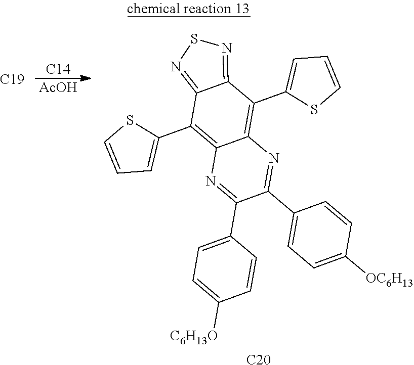


| TABLE 1 |
| embodiments of organic semiconducting compounds |
 |
DP1 |
 |
DP2 |
 |
DP3 |
 |
DP4 |
 |
DP5 |
 |
DP6 |
 |
DP7 |
 |
DP8 |
 |
DP9 |
 |
DP10 |
 |
DP11 |
 |
DP12 |
 |
DP13 |


| TABLE 2 |
| measurement of absorption spectrum and test results of electrochemical |
| properties of the respective samples |
| ε | ||||||||
| λsoln max | λfilm max | λfilm onset | (105 | Eg opt | HOMO | LUMO | ||
| material | (nm) | (nm) | (nm) | cm−1M−1) | (eV) | (eV) | (eV) | solubility |
| DP2 | 1108 | 1128 | 1358 | 0.243 | 0.91 | −5.05 | −4.14 | ◯ |
| DP5 | 1054 | 1118 | 1619 | 0.268 | 0.77 | −4.68 | −3.91 | ◯ |
| PCBOTQ | 532 | 564 | 816 | — | 1.52 | −5.16 | −3.64 | X |
| PTTQ(BO) | — | 1145 | 1426 | — | 0.87 | −4.87 | −4.00 | X |
PCBOTQ of the
HOMO=−|4.71+E ox −E ferroncene|
LUMO=HOMO+E g opt
Test results of the respective samples are shown in table 2.
| TABLE 3 |
| Electrical tests of organic photoelectric components containing the |
| present organic semiconducting compounds |
| Wavelength | 1100 | 1100 | 1100 | 1100 | 1100 | 1100 | ||
| (nm) | ||||||||
| Active | PCBOTQ: | PTTQ(BO): | PTZBTTT- | P4: PC61BM | DP2: N1 | DP5: N1 | ||
| layer | PC71BM | PC71BM | BDT: | |||||
| PC61BM | ||||||||
| Thickness | 80-90 | 300 | ~70 | 385 | 100 | 100 | ||
| (nm) | ||||||||
| Band | 1.52 | 0.86 | 1.10 | 0.85 | 0.91 | 0.77 | ||
| gap(eV) | ||||||||
| Structure | Conventional | Inverted | Conventional | Inverted | Inverted | Inverted | ||
| ETL | LiF | ZnO | PFN | PEIE | AZO | AZO | ||
| HTL | PEDOT | MoO3 | PEDOT: PSS | MoO3 | MoO3 | MoO3 | ||
| Solvents | CB | CB | o-DCB | CB, CF, | o-xylene | o-xylene | ||
| for process | DIO | |||||||
| Jd (A/cm2) | — | 10−4@ −2 | 10−6@ −2 |
10−5 @ | 10−6 @ | 10−6 @ | ||
| V | −1.5 V | −2 V | −2 V | |||||
| EQE | No response | ~17%@ | No response | ~7% @ 0 V | 20.0% @ | 21.5% @ | ||
| −2 V | −10 V | −10 V | ||||||
| Ref. | J. Phys. | J. Mater. | J. Phys. | Polym. | This | This | ||
| Chem. C | Chem. C, | Chem. C | Chem., | | work | |||
| 2012, 116, | 2020, 8, | 2013, 117, | 2017, 8, | |||||
| 8379-8386. | 10098- | 6537-6543 | 2922-2930 | |||||
| 10103 | ||||||||
| TABLE 4 |
| Electrical tests of organic photoelectric components containing the |
| present organic semiconducting compounds |
| Wavelength | 700 | 700 | 700 | 700 | 700 | 700 | ||
| (nm) | ||||||||
| Active layer | PCBOTQ: | PTTQ(BO): | PTZBTTT- | P4: | DP2: N1 | DP5: N1 | ||
| PC71BM | PC71BM | BDT: | PC6BM | |||||
| PC61BM | ||||||||
| Thickness | 80-90 | 300 | ~70 | 385 | 100 | 100 | ||
| (nm) | ||||||||
| Band gap(eV) | 1.52 | 0.86 | 1.10 | 0.85 | 0.91 | 0.77 | ||
| Structure | Conventional | Inverted | Conventional | Inverted | Inverted | Inverted | ||
| ETL | LiF | ZnO | PFN | PEIE | AZO | AZO | ||
| HTL | PEDOT | MoO3 | PEDOT:PSS | MoO3 | MoO3 | MoO3 | ||
| Solvents for | CB | CB | o-DCB | CB, CF, | o-xylene | o-xylene | ||
| process | DIO | |||||||
| Jd (A/cm2) | — | 10−4 @ −2 |
10−6 @ − |
10−5 @ | 10−6 @ | 10−6 @ | ||
| −1.5 V | −2 V | −2 V | ||||||
| EQE | ~16% @ 0 V | ~7% @ −2 V | ~17% @ 0 V | ~9% @ | 39.5% | 33.6% | ||
| 0 V | @ −10 V | @ −10 V | ||||||
| Ref. | J. Phys. | J. Mater. | J. Phys. | Polym. | This | This | ||
| Chem. C | Chem. C, | Chem. C | Chem., | | work | |||
| 2012, 116, | 2020, 8, | 2013, 117, | 2017, 8, | |||||
| 8379-8386. | 10098- | 6537-6543 | 2922- | |||||
| 10103 | 2930 | |||||||
Claims (12)


Priority Applications (1)
| Application Number | Priority Date | Filing Date | Title |
|---|---|---|---|
| US17/930,868 US11925101B2 (en) | 2021-09-15 | 2022-09-09 | Organic semiconducting compound and the organic photoelectric components using the same |
Applications Claiming Priority (2)
| Application Number | Priority Date | Filing Date | Title |
|---|---|---|---|
| US202163244362P | 2021-09-15 | 2021-09-15 | |
| US17/930,868 US11925101B2 (en) | 2021-09-15 | 2022-09-09 | Organic semiconducting compound and the organic photoelectric components using the same |
Publications (2)
| Publication Number | Publication Date |
|---|---|
| US20230126747A1 US20230126747A1 (en) | 2023-04-27 |
| US11925101B2 true US11925101B2 (en) | 2024-03-05 |
Family
ID=85523572
Family Applications (1)
| Application Number | Title | Priority Date | Filing Date |
|---|---|---|---|
| US17/930,868 Active US11925101B2 (en) | 2021-09-15 | 2022-09-09 | Organic semiconducting compound and the organic photoelectric components using the same |
Country Status (4)
| Country | Link |
|---|---|
| US (1) | US11925101B2 (en) |
| JP (1) | JP2023055647A (en) |
| CN (1) | CN115819733A (en) |
| TW (1) | TW202313634A (en) |
Citations (11)
| Publication number | Priority date | Publication date | Assignee | Title |
|---|---|---|---|---|
| WO2011025454A1 (en) | 2009-08-28 | 2011-03-03 | Agency For Science, Technology And Research | Ambipolar polymeric semiconductor materials and organic electronic devices |
| JP2013199590A (en) | 2012-03-26 | 2013-10-03 | Toray Ind Inc | Electron-donating organic material, material for photovoltaic element using the same, and photovoltaic element |
| TW201509983A (en) | 2013-06-21 | 2015-03-16 | Merck Patent Gmbh | Conjugated polymers |
| WO2017157782A1 (en) | 2016-03-15 | 2017-09-21 | Merck Patent Gmbh | Organic semiconductors |
| TW201736430A (en) | 2015-12-18 | 2017-10-16 | 馬克專利公司 | Thiadiazolopyridine polymers, their synthesis and their use |
| JP2018521151A (en) | 2015-05-06 | 2018-08-02 | メルク・パテント・ゲゼルシヤフト・ミツト・ベシユレンクテル・ハフツングMerck Patent GmbH | Thiadiazoloquinoxaline derivative |
| CN109790176A (en) | 2016-10-05 | 2019-05-21 | 默克专利有限公司 | Organic semiconductor compound |
| CN112920204A (en) | 2021-02-08 | 2021-06-08 | 中国科学院化学研究所 | Electron acceptor organic solar cell material based on thiadiazole quinoxaline structure and preparation method and application thereof |
| JP2023024349A (en) | 2021-08-06 | 2023-02-16 | レイナジー テック インコーポレイション | Conjugated polymer material and organic photoelectronic device utilizing the same |
| JP2023024300A (en) | 2021-08-06 | 2023-02-16 | レイナジー テック インコーポレイション | Low energy gap small molecule material and organic photoelectronic device utilizing the same |
| JP2023033222A (en) | 2021-08-27 | 2023-03-09 | レイナジー テック インコーポレイション | Organic semiconductor compound and organic photoelectric element including the same |
-
2022
- 2022-09-07 TW TW111133944A patent/TW202313634A/en unknown
- 2022-09-09 US US17/930,868 patent/US11925101B2/en active Active
- 2022-09-14 JP JP2022146183A patent/JP2023055647A/en active Pending
- 2022-09-14 CN CN202211117207.8A patent/CN115819733A/en active Pending
Patent Citations (16)
| Publication number | Priority date | Publication date | Assignee | Title |
|---|---|---|---|---|
| WO2011025454A1 (en) | 2009-08-28 | 2011-03-03 | Agency For Science, Technology And Research | Ambipolar polymeric semiconductor materials and organic electronic devices |
| TW201111411A (en) | 2009-08-28 | 2011-04-01 | Agency Science Tech & Res | Ambipolar polymeric semiconductor materials and organic electronic devices |
| JP2013199590A (en) | 2012-03-26 | 2013-10-03 | Toray Ind Inc | Electron-donating organic material, material for photovoltaic element using the same, and photovoltaic element |
| TW201509983A (en) | 2013-06-21 | 2015-03-16 | Merck Patent Gmbh | Conjugated polymers |
| JP2016524010A (en) | 2013-06-21 | 2016-08-12 | メルク パテント ゲーエムベーハー | Conjugated polymer |
| JP2018521151A (en) | 2015-05-06 | 2018-08-02 | メルク・パテント・ゲゼルシヤフト・ミツト・ベシユレンクテル・ハフツングMerck Patent GmbH | Thiadiazoloquinoxaline derivative |
| TW201736430A (en) | 2015-12-18 | 2017-10-16 | 馬克專利公司 | Thiadiazolopyridine polymers, their synthesis and their use |
| JP2019502001A (en) | 2015-12-18 | 2019-01-24 | メルク パテント ゲゼルシャフト ミット ベシュレンクテル ハフツングMerck Patent Gesellschaft mit beschraenkter Haftung | Thiadiazolopyridine polymers, their synthesis and their use |
| TW201808964A (en) | 2016-03-15 | 2018-03-16 | 麥克專利有限公司 | Organic semiconductors |
| WO2017157782A1 (en) | 2016-03-15 | 2017-09-21 | Merck Patent Gmbh | Organic semiconductors |
| CN109790176A (en) | 2016-10-05 | 2019-05-21 | 默克专利有限公司 | Organic semiconductor compound |
| JP2019536744A (en) | 2016-10-05 | 2019-12-19 | メルク パテント ゲーエムベーハー | Organic semiconductor compounds |
| CN112920204A (en) | 2021-02-08 | 2021-06-08 | 中国科学院化学研究所 | Electron acceptor organic solar cell material based on thiadiazole quinoxaline structure and preparation method and application thereof |
| JP2023024349A (en) | 2021-08-06 | 2023-02-16 | レイナジー テック インコーポレイション | Conjugated polymer material and organic photoelectronic device utilizing the same |
| JP2023024300A (en) | 2021-08-06 | 2023-02-16 | レイナジー テック インコーポレイション | Low energy gap small molecule material and organic photoelectronic device utilizing the same |
| JP2023033222A (en) | 2021-08-27 | 2023-03-09 | レイナジー テック インコーポレイション | Organic semiconductor compound and organic photoelectric element including the same |
Non-Patent Citations (9)
| Title |
|---|
| Frederick Verstraeten, et al., Efficient and Readily Tuneable Near-Infrared Photodetection Up to 1500 NM Enabled by Thiadiazoloquinoxaline-Based Push-Pull Type Conjugated Polymers, J. Mater. Chem. C, 2020, 8, 10098. |
| Japan Patent Office Official action, dated Oct. 24, 2023. |
| Jinfeng Han "Low-Bandgap Polymers for High-Performance Photodiodes with Maximal EQE near 1200 nm and Broad Spectral Response from 300 to 1700 nm" Adv. Optical Mater. 2018, 6, 1800038 (Year: 2018). * |
| Jinfeng Han et al., "1. Low-Bandgap Terpolymers for High-Gain Photodiodes with High Detectivity and Responsivity from 300 nm to 1600 nm", 2018, Wiley-VCH Verlag Gmbh & Co. KGaA, Weinheim. |
| Qiang Peng "Donor-ð-Acceptor Conjugated Copolymers for Photovoltaic Applications: Tuning the Open-Circuit Voltage by Adjusting the Donor/Acceptor Ratio" J. Phys. Chem. B 2008, 112, 2801-2808 (Year: 2008). * |
| Richard Hildner "π-Conjugated Donor Polymers: Structure Formation and Morphology in Solution, Bulk and Photovoltaic Blends" Adv. Energy Mater. 2017, 7, 1700314 (Year: 2017). * |
| Taiwan Intellectual Property Office official action, dated Nov. 16, 2023. |
| Yoonkyoo Lee, et al., Fine-Tuning of Molecular Energy Level of Alternating Copolymers on the Basis of [1,2,5] Thiadiazolo [3,4-g] Quinoxaline Derivatives for Polymer Photovoltaics, J. Phys. Chem. C, 2012, 116, 8379-8386. |
| Yunpeng Qin "Highly Efficient Fullerene-Free Polymer Solar Cells Fabricated with Polythiophene Derivative" Adv. Mater. 2016, 28, 9416-9422 (Year: 2016). * |
Also Published As
| Publication number | Publication date |
|---|---|
| TW202313634A (en) | 2023-04-01 |
| JP2023055647A (en) | 2023-04-18 |
| CN115819733A (en) | 2023-03-21 |
| US20230126747A1 (en) | 2023-04-27 |
Similar Documents
| Publication | Publication Date | Title |
|---|---|---|
| US11233207B2 (en) | Narrow bandgap non-fullerene acceptors and devices including narrow bandgap non-fullerene acceptors | |
| US9783634B2 (en) | Synthesis of photovoltaic conjugated polymers | |
| US10355212B2 (en) | Polymer and solar cell using the same | |
| JP2015507644A (en) | Diketopyrrolopyrrole polymers for use in organic semiconductor devices | |
| JP2018046096A (en) | Photoelectric conversion element | |
| US20230121184A1 (en) | Organic semiconducting compound and the organic photoelectric components using the same | |
| US20220396661A1 (en) | Novel polymer and organic electronic device using same | |
| Lim et al. | Synthesis and photovoltaic properties of a thienylenevinylene and diketopyrrolopyrrole copolymer with high mobility | |
| US20210230130A1 (en) | Non-fullerene acceptor compound containing benzoselenadiazole and organic optoelectronic device including the same | |
| Cui et al. | From transistors to phototransistors by tailoring the polymer stacking | |
| Liu et al. | Synthesis of low band-gap 2D conjugated polymers and their application for organic field effect transistors and solar cells | |
| US11925101B2 (en) | Organic semiconducting compound and the organic photoelectric components using the same | |
| US20230113502A1 (en) | Low energy gap small molecule material and organic optoelectronic device using the same | |
| Li et al. | Molecular Engineering of Polymeric Hole-Transporting Materials for Efficient and Stable Perovskite Solar Cells | |
| Huang et al. | Low band‐gap D–A conjugated copolymers based on anthradithiophene and diketopyrrolopyrrole for polymer solar cells and field‐effect transistors | |
| KR102446165B1 (en) | Compound containing aryloxy akyl group and organic electronic device using them | |
| Li et al. | A two-dimension medium band gap conjugated polymer based on 5, 10-bis (alkylthien-2-yl) dithieno [3, 2-d: 3′, 2′-d′] benzo [1, 2-b: 4, 5-b′] dithiophene: Synthesis and photovoltaic application | |
| US11957051B2 (en) | Organic semiconductor mixture and organic optoelectronic device containing the same | |
| Ganesamoorthy et al. | Synthesis and studies of bay‐substituted perylene diimide‐based D–A–D‐type SM acceptors for OSC and antimicrobial applications | |
| US20230131130A1 (en) | Organic semiconducting compound and organic photoelectric components using the same | |
| US9634252B2 (en) | Polymer and solar cell using the same | |
| Gayathri et al. | Pentyl side chain-based benzoditiophene π-conjugated polymer for non-halogenated solvent processed organic solar cells | |
| Ganesamoorthy et al. | Perylene-diimide based donor–acceptor–donor type small-molecule acceptors for solution-processable organic solar cells | |
| US20240122055A1 (en) | Organic semiconducting compound and organic optoelectronic devices using the same | |
| JP2024027112A (en) | Organic semiconducting polymers and organic optoelectronic devices containing them |
Legal Events
| Date | Code | Title | Description |
|---|---|---|---|
| FEPP | Fee payment procedure |
Free format text: ENTITY STATUS SET TO UNDISCOUNTED (ORIGINAL EVENT CODE: BIG.); ENTITY STATUS OF PATENT OWNER: SMALL ENTITY |
|
| FEPP | Fee payment procedure |
Free format text: ENTITY STATUS SET TO SMALL (ORIGINAL EVENT CODE: SMAL); ENTITY STATUS OF PATENT OWNER: SMALL ENTITY |
|
| AS | Assignment |
Owner name: RAYNERGY TEK INCORPORATION, TAIWAN Free format text: ASSIGNMENT OF ASSIGNORS INTEREST;ASSIGNORS:LI, WEI-LONG;HSIAO, YU-TANG;TSAI, CHIA-HUA;AND OTHERS;REEL/FRAME:063904/0672 Effective date: 20220809 |
|
| STPP | Information on status: patent application and granting procedure in general |
Free format text: RESPONSE TO NON-FINAL OFFICE ACTION ENTERED AND FORWARDED TO EXAMINER |
|
| STPP | Information on status: patent application and granting procedure in general |
Free format text: FINAL REJECTION MAILED |
|
| STPP | Information on status: patent application and granting procedure in general |
Free format text: DOCKETED NEW CASE - READY FOR EXAMINATION |
|
| STPP | Information on status: patent application and granting procedure in general |
Free format text: NOTICE OF ALLOWANCE MAILED -- APPLICATION RECEIVED IN OFFICE OF PUBLICATIONS |
|
| STPP | Information on status: patent application and granting procedure in general |
Free format text: AWAITING TC RESP., ISSUE FEE NOT PAID |
|
| STPP | Information on status: patent application and granting procedure in general |
Free format text: NOTICE OF ALLOWANCE MAILED -- APPLICATION RECEIVED IN OFFICE OF PUBLICATIONS |
|
| STPP | Information on status: patent application and granting procedure in general |
Free format text: PUBLICATIONS -- ISSUE FEE PAYMENT VERIFIED |
|
| STCF | Information on status: patent grant |
Free format text: PATENTED CASE |