US9634252B2 - Polymer and solar cell using the same - Google Patents
Polymer and solar cell using the same Download PDFInfo
- Publication number
- US9634252B2 US9634252B2 US15/072,834 US201615072834A US9634252B2 US 9634252 B2 US9634252 B2 US 9634252B2 US 201615072834 A US201615072834 A US 201615072834A US 9634252 B2 US9634252 B2 US 9634252B2
- Authority
- US
- United States
- Prior art keywords
- group
- polymer
- substituted
- solar cell
- unsubstituted
- Prior art date
- Legal status (The legal status is an assumption and is not a legal conclusion. Google has not performed a legal analysis and makes no representation as to the accuracy of the status listed.)
- Active
Links
- 229920000642 polymer Polymers 0.000 title claims abstract description 131
- 125000002915 carbonyl group Chemical group [*:2]C([*:1])=O 0.000 claims abstract description 30
- 125000003118 aryl group Chemical group 0.000 claims abstract description 27
- 125000000217 alkyl group Chemical group 0.000 claims abstract description 26
- 125000000472 sulfonyl group Chemical group *S(*)(=O)=O 0.000 claims abstract description 18
- 125000000475 sulfinyl group Chemical group [*:2]S([*:1])=O 0.000 claims abstract description 17
- 125000002252 acyl group Chemical group 0.000 claims abstract description 15
- QVGXLLKOCUKJST-UHFFFAOYSA-N atomic oxygen Chemical group [O] QVGXLLKOCUKJST-UHFFFAOYSA-N 0.000 claims abstract description 14
- 229910052760 oxygen Inorganic materials 0.000 claims abstract description 14
- 239000001301 oxygen Substances 0.000 claims abstract description 14
- 125000001072 heteroaryl group Chemical group 0.000 claims abstract description 12
- 239000011669 selenium Chemical group 0.000 claims abstract description 12
- BUGBHKTXTAQXES-UHFFFAOYSA-N Selenium Chemical group [Se] BUGBHKTXTAQXES-UHFFFAOYSA-N 0.000 claims abstract description 11
- NINIDFKCEFEMDL-UHFFFAOYSA-N Sulfur Chemical group [S] NINIDFKCEFEMDL-UHFFFAOYSA-N 0.000 claims abstract description 11
- 229910052736 halogen Inorganic materials 0.000 claims abstract description 11
- 229910052711 selenium Inorganic materials 0.000 claims abstract description 11
- 229910052717 sulfur Inorganic materials 0.000 claims abstract description 11
- 239000011593 sulfur Chemical group 0.000 claims abstract description 11
- 150000002367 halogens Chemical group 0.000 claims abstract description 10
- 239000001257 hydrogen Substances 0.000 claims abstract description 9
- 229910052739 hydrogen Inorganic materials 0.000 claims abstract description 9
- 238000006243 chemical reaction Methods 0.000 claims description 51
- 238000004132 cross linking Methods 0.000 claims description 31
- 125000001424 substituent group Chemical group 0.000 claims description 25
- 239000000872 buffer Substances 0.000 claims description 19
- 229910052786 argon Inorganic materials 0.000 claims description 14
- 125000004429 atom Chemical group 0.000 claims description 13
- 125000004093 cyano group Chemical group *C#N 0.000 claims description 9
- 125000000449 nitro group Chemical group [O-][N+](*)=O 0.000 claims description 9
- 125000004435 hydrogen atom Chemical class [H]* 0.000 claims description 7
- 239000011368 organic material Substances 0.000 claims description 7
- 229910052727 yttrium Inorganic materials 0.000 claims description 6
- 150000002431 hydrogen Chemical group 0.000 abstract 1
- 239000010410 layer Substances 0.000 description 203
- 239000000463 material Substances 0.000 description 131
- 239000004065 semiconductor Substances 0.000 description 100
- 150000001875 compounds Chemical class 0.000 description 96
- 238000000605 extraction Methods 0.000 description 90
- 238000000034 method Methods 0.000 description 65
- YXFVVABEGXRONW-UHFFFAOYSA-N Toluene Chemical compound CC1=CC=CC=C1 YXFVVABEGXRONW-UHFFFAOYSA-N 0.000 description 58
- 239000000178 monomer Substances 0.000 description 51
- UHOVQNZJYSORNB-UHFFFAOYSA-N Benzene Chemical compound C1=CC=CC=C1 UHOVQNZJYSORNB-UHFFFAOYSA-N 0.000 description 48
- -1 poly(3-hexylthiophene-2,5-diyl) Polymers 0.000 description 47
- 239000000243 solution Substances 0.000 description 43
- 239000007787 solid Substances 0.000 description 42
- 239000010408 film Substances 0.000 description 39
- 239000002904 solvent Substances 0.000 description 39
- VLKZOEOYAKHREP-UHFFFAOYSA-N n-Hexane Chemical compound CCCCCC VLKZOEOYAKHREP-UHFFFAOYSA-N 0.000 description 36
- 239000000654 additive Substances 0.000 description 34
- 230000000996 additive effect Effects 0.000 description 34
- 239000000758 substrate Substances 0.000 description 34
- XEKOWRVHYACXOJ-UHFFFAOYSA-N Ethyl acetate Chemical compound CCOC(C)=O XEKOWRVHYACXOJ-UHFFFAOYSA-N 0.000 description 33
- 239000010409 thin film Substances 0.000 description 29
- 230000015572 biosynthetic process Effects 0.000 description 24
- 238000003786 synthesis reaction Methods 0.000 description 23
- 230000002194 synthesizing effect Effects 0.000 description 23
- MVPPADPHJFYWMZ-UHFFFAOYSA-N chlorobenzene Chemical compound ClC1=CC=CC=C1 MVPPADPHJFYWMZ-UHFFFAOYSA-N 0.000 description 22
- 238000000576 coating method Methods 0.000 description 22
- 0 *N1CC2=C([Y]1)C1=C(C)CC(C)=C1C2 Chemical compound *N1CC2=C([Y]1)C1=C(C)CC(C)=C1C2 0.000 description 21
- ZMXDDKWLCZADIW-UHFFFAOYSA-N N,N-Dimethylformamide Chemical compound CN(C)C=O ZMXDDKWLCZADIW-UHFFFAOYSA-N 0.000 description 21
- XKRFYHLGVUSROY-UHFFFAOYSA-N Argon Chemical compound [Ar] XKRFYHLGVUSROY-UHFFFAOYSA-N 0.000 description 20
- 239000000284 extract Substances 0.000 description 17
- 238000010438 heat treatment Methods 0.000 description 17
- 239000011248 coating agent Substances 0.000 description 16
- 230000000875 corresponding effect Effects 0.000 description 16
- 239000011521 glass Substances 0.000 description 16
- OKKJLVBELUTLKV-UHFFFAOYSA-N Methanol Chemical compound OC OKKJLVBELUTLKV-UHFFFAOYSA-N 0.000 description 15
- YTPLMLYBLZKORZ-UHFFFAOYSA-N Thiophene Chemical compound C=1C=CSC=1 YTPLMLYBLZKORZ-UHFFFAOYSA-N 0.000 description 15
- HEDRZPFGACZZDS-UHFFFAOYSA-N Chloroform Chemical compound ClC(Cl)Cl HEDRZPFGACZZDS-UHFFFAOYSA-N 0.000 description 14
- KDLHZDBZIXYQEI-UHFFFAOYSA-N Palladium Chemical compound [Pd] KDLHZDBZIXYQEI-UHFFFAOYSA-N 0.000 description 14
- WYURNTSHIVDZCO-UHFFFAOYSA-N Tetrahydrofuran Chemical compound C1CCOC1 WYURNTSHIVDZCO-UHFFFAOYSA-N 0.000 description 14
- HEDRZPFGACZZDS-MICDWDOJSA-N Trichloro(2H)methane Chemical compound [2H]C(Cl)(Cl)Cl HEDRZPFGACZZDS-MICDWDOJSA-N 0.000 description 14
- IJGRMHOSHXDMSA-UHFFFAOYSA-N Atomic nitrogen Chemical compound N#N IJGRMHOSHXDMSA-UHFFFAOYSA-N 0.000 description 12
- 230000006866 deterioration Effects 0.000 description 12
- 238000010521 absorption reaction Methods 0.000 description 11
- 238000009835 boiling Methods 0.000 description 11
- 230000006870 function Effects 0.000 description 11
- 229910052751 metal Inorganic materials 0.000 description 11
- 239000002184 metal Substances 0.000 description 11
- 239000012071 phase Substances 0.000 description 11
- 238000006116 polymerization reaction Methods 0.000 description 11
- 238000010992 reflux Methods 0.000 description 11
- ZCYVEMRRCGMTRW-UHFFFAOYSA-N 7553-56-2 Chemical compound [I] ZCYVEMRRCGMTRW-UHFFFAOYSA-N 0.000 description 10
- 230000000052 comparative effect Effects 0.000 description 10
- 239000012299 nitrogen atmosphere Substances 0.000 description 10
- 229920000301 poly(3-hexylthiophene-2,5-diyl) polymer Polymers 0.000 description 10
- XMWRBQBLMFGWIX-UHFFFAOYSA-N C60 fullerene Chemical class C12=C3C(C4=C56)=C7C8=C5C5=C9C%10=C6C6=C4C1=C1C4=C6C6=C%10C%10=C9C9=C%11C5=C8C5=C8C7=C3C3=C7C2=C1C1=C2C4=C6C4=C%10C6=C9C9=C%11C5=C5C8=C3C3=C7C1=C1C2=C4C6=C2C9=C5C3=C12 XMWRBQBLMFGWIX-UHFFFAOYSA-N 0.000 description 9
- XLOMVQKBTHCTTD-UHFFFAOYSA-N Zinc monoxide Chemical compound [Zn]=O XLOMVQKBTHCTTD-UHFFFAOYSA-N 0.000 description 9
- 229960001701 chloroform Drugs 0.000 description 9
- 239000002243 precursor Substances 0.000 description 9
- FCEHBMOGCRZNNI-UHFFFAOYSA-N 1-benzothiophene Chemical group C1=CC=C2SC=CC2=C1 FCEHBMOGCRZNNI-UHFFFAOYSA-N 0.000 description 8
- 238000005160 1H NMR spectroscopy Methods 0.000 description 8
- CSCPPACGZOOCGX-UHFFFAOYSA-N Acetone Chemical compound CC(C)=O CSCPPACGZOOCGX-UHFFFAOYSA-N 0.000 description 8
- OKTJSMMVPCPJKN-UHFFFAOYSA-N Carbon Chemical compound [C] OKTJSMMVPCPJKN-UHFFFAOYSA-N 0.000 description 8
- 238000005481 NMR spectroscopy Methods 0.000 description 8
- PXHVJJICTQNCMI-UHFFFAOYSA-N Nickel Chemical compound [Ni] PXHVJJICTQNCMI-UHFFFAOYSA-N 0.000 description 8
- 238000000944 Soxhlet extraction Methods 0.000 description 8
- GWEVSGVZZGPLCZ-UHFFFAOYSA-N Titan oxide Chemical compound O=[Ti]=O GWEVSGVZZGPLCZ-UHFFFAOYSA-N 0.000 description 8
- 239000000460 chlorine Substances 0.000 description 8
- 230000006872 improvement Effects 0.000 description 8
- 229910052740 iodine Inorganic materials 0.000 description 8
- 239000011572 manganese Substances 0.000 description 8
- 238000004519 manufacturing process Methods 0.000 description 8
- 229910044991 metal oxide Inorganic materials 0.000 description 8
- 150000004706 metal oxides Chemical class 0.000 description 8
- 238000003756 stirring Methods 0.000 description 8
- 238000002371 ultraviolet--visible spectrum Methods 0.000 description 8
- XLYOFNOQVPJJNP-UHFFFAOYSA-N water Substances O XLYOFNOQVPJJNP-UHFFFAOYSA-N 0.000 description 8
- WKBOTKDWSSQWDR-UHFFFAOYSA-N Bromine atom Chemical compound [Br] WKBOTKDWSSQWDR-UHFFFAOYSA-N 0.000 description 7
- LFQSCWFLJHTTHZ-UHFFFAOYSA-N Ethanol Chemical compound CCO LFQSCWFLJHTTHZ-UHFFFAOYSA-N 0.000 description 7
- 238000006619 Stille reaction Methods 0.000 description 7
- 238000001035 drying Methods 0.000 description 7
- 125000005842 heteroatom Chemical class 0.000 description 7
- 229910052763 palladium Inorganic materials 0.000 description 7
- 238000004528 spin coating Methods 0.000 description 7
- YLQBMQCUIZJEEH-UHFFFAOYSA-N tetrahydrofuran Natural products C=1C=COC=1 YLQBMQCUIZJEEH-UHFFFAOYSA-N 0.000 description 7
- ZWEHNKRNPOVVGH-UHFFFAOYSA-N 2-Butanone Chemical compound CCC(C)=O ZWEHNKRNPOVVGH-UHFFFAOYSA-N 0.000 description 6
- RTZKZFJDLAIYFH-UHFFFAOYSA-N Diethyl ether Chemical compound CCOCC RTZKZFJDLAIYFH-UHFFFAOYSA-N 0.000 description 6
- HEMHJVSKTPXQMS-UHFFFAOYSA-M Sodium hydroxide Chemical compound [OH-].[Na+] HEMHJVSKTPXQMS-UHFFFAOYSA-M 0.000 description 6
- 238000006069 Suzuki reaction reaction Methods 0.000 description 6
- 238000000137 annealing Methods 0.000 description 6
- 229910052799 carbon Inorganic materials 0.000 description 6
- 239000003054 catalyst Substances 0.000 description 6
- 229910052801 chlorine Inorganic materials 0.000 description 6
- 238000011156 evaluation Methods 0.000 description 6
- 239000011630 iodine Substances 0.000 description 6
- 239000000203 mixture Substances 0.000 description 6
- 229910052757 nitrogen Inorganic materials 0.000 description 6
- 150000002894 organic compounds Chemical class 0.000 description 6
- 239000003960 organic solvent Substances 0.000 description 6
- 238000005191 phase separation Methods 0.000 description 6
- 125000001997 phenyl group Chemical group [H]C1=C([H])C([H])=C(*)C([H])=C1[H] 0.000 description 6
- OGIDPMRJRNCKJF-UHFFFAOYSA-N titanium oxide Inorganic materials [Ti]=O OGIDPMRJRNCKJF-UHFFFAOYSA-N 0.000 description 6
- 238000002834 transmittance Methods 0.000 description 6
- RIOQSEWOXXDEQQ-UHFFFAOYSA-N triphenylphosphine Chemical compound C1=CC=CC=C1P(C=1C=CC=CC=1)C1=CC=CC=C1 RIOQSEWOXXDEQQ-UHFFFAOYSA-N 0.000 description 6
- 238000001771 vacuum deposition Methods 0.000 description 6
- VEXZGXHMUGYJMC-UHFFFAOYSA-N Hydrochloric acid Chemical compound Cl VEXZGXHMUGYJMC-UHFFFAOYSA-N 0.000 description 5
- FXHOOIRPVKKKFG-UHFFFAOYSA-N N,N-Dimethylacetamide Chemical compound CN(C)C(C)=O FXHOOIRPVKKKFG-UHFFFAOYSA-N 0.000 description 5
- 229910052782 aluminium Inorganic materials 0.000 description 5
- XAGFODPZIPBFFR-UHFFFAOYSA-N aluminium Chemical compound [Al] XAGFODPZIPBFFR-UHFFFAOYSA-N 0.000 description 5
- 239000007864 aqueous solution Substances 0.000 description 5
- GDTBXPJZTBHREO-UHFFFAOYSA-N bromine Substances BrBr GDTBXPJZTBHREO-UHFFFAOYSA-N 0.000 description 5
- 229910052794 bromium Inorganic materials 0.000 description 5
- 238000001816 cooling Methods 0.000 description 5
- 238000005859 coupling reaction Methods 0.000 description 5
- 230000000694 effects Effects 0.000 description 5
- 125000001495 ethyl group Chemical group [H]C([H])([H])C([H])([H])* 0.000 description 5
- 239000010931 gold Substances 0.000 description 5
- 150000003949 imides Chemical class 0.000 description 5
- 125000002496 methyl group Chemical group [H]C([H])([H])* 0.000 description 5
- 229920001343 polytetrafluoroethylene Polymers 0.000 description 5
- 239000004810 polytetrafluoroethylene Substances 0.000 description 5
- 238000010248 power generation Methods 0.000 description 5
- VYPSYNLAJGMNEJ-UHFFFAOYSA-N silicon dioxide Inorganic materials O=[Si]=O VYPSYNLAJGMNEJ-UHFFFAOYSA-N 0.000 description 5
- 238000004544 sputter deposition Methods 0.000 description 5
- 229910052718 tin Inorganic materials 0.000 description 5
- 238000005406 washing Methods 0.000 description 5
- RFFLAFLAYFXFSW-UHFFFAOYSA-N 1,2-dichlorobenzene Chemical compound ClC1=CC=CC=C1Cl RFFLAFLAYFXFSW-UHFFFAOYSA-N 0.000 description 4
- RYHBNJHYFVUHQT-UHFFFAOYSA-N 1,4-Dioxane Chemical compound C1COCCO1 RYHBNJHYFVUHQT-UHFFFAOYSA-N 0.000 description 4
- UUIMDJFBHNDZOW-UHFFFAOYSA-N 2-tert-butylpyridine Chemical compound CC(C)(C)C1=CC=CC=N1 UUIMDJFBHNDZOW-UHFFFAOYSA-N 0.000 description 4
- ZAMOUSCENKQFHK-UHFFFAOYSA-N Chlorine atom Chemical compound [Cl] ZAMOUSCENKQFHK-UHFFFAOYSA-N 0.000 description 4
- PCLIMKBDDGJMGD-UHFFFAOYSA-N N-bromosuccinimide Chemical compound BrN1C(=O)CCC1=O PCLIMKBDDGJMGD-UHFFFAOYSA-N 0.000 description 4
- UFWIBTONFRDIAS-UHFFFAOYSA-N Naphthalene Chemical compound C1=CC=CC2=CC=CC=C21 UFWIBTONFRDIAS-UHFFFAOYSA-N 0.000 description 4
- 230000002776 aggregation Effects 0.000 description 4
- 238000004220 aggregation Methods 0.000 description 4
- 150000001335 aliphatic alkanes Chemical class 0.000 description 4
- 229910052783 alkali metal Inorganic materials 0.000 description 4
- 239000012300 argon atmosphere Substances 0.000 description 4
- 239000012298 atmosphere Substances 0.000 description 4
- 125000000484 butyl group Chemical group [H]C([*])([H])C([H])([H])C([H])([H])C([H])([H])[H] 0.000 description 4
- XJHCXCQVJFPJIK-UHFFFAOYSA-M caesium fluoride Chemical compound [F-].[Cs+] XJHCXCQVJFPJIK-UHFFFAOYSA-M 0.000 description 4
- 125000001309 chloro group Chemical group Cl* 0.000 description 4
- 238000004440 column chromatography Methods 0.000 description 4
- 229920001940 conductive polymer Polymers 0.000 description 4
- JHIVVAPYMSGYDF-UHFFFAOYSA-N cyclohexanone Chemical compound O=C1CCCCC1 JHIVVAPYMSGYDF-UHFFFAOYSA-N 0.000 description 4
- PCHJSUWPFVWCPO-UHFFFAOYSA-N gold Chemical compound [Au] PCHJSUWPFVWCPO-UHFFFAOYSA-N 0.000 description 4
- 229910052737 gold Inorganic materials 0.000 description 4
- 125000005843 halogen group Chemical group 0.000 description 4
- 230000001771 impaired effect Effects 0.000 description 4
- 229910010272 inorganic material Inorganic materials 0.000 description 4
- 239000003446 ligand Substances 0.000 description 4
- PQXKHYXIUOZZFA-UHFFFAOYSA-M lithium fluoride Chemical compound [Li+].[F-] PQXKHYXIUOZZFA-UHFFFAOYSA-M 0.000 description 4
- 229910052759 nickel Inorganic materials 0.000 description 4
- IOQPZZOEVPZRBK-UHFFFAOYSA-N octan-1-amine Chemical compound CCCCCCCCN IOQPZZOEVPZRBK-UHFFFAOYSA-N 0.000 description 4
- 125000002347 octyl group Chemical group [H]C([*])([H])C([H])([H])C([H])([H])C([H])([H])C([H])([H])C([H])([H])C([H])([H])C([H])([H])[H] 0.000 description 4
- NFHFRUOZVGFOOS-UHFFFAOYSA-N palladium;triphenylphosphane Chemical compound [Pd].C1=CC=CC=C1P(C=1C=CC=CC=1)C1=CC=CC=C1.C1=CC=CC=C1P(C=1C=CC=CC=1)C1=CC=CC=C1.C1=CC=CC=C1P(C=1C=CC=CC=1)C1=CC=CC=C1.C1=CC=CC=C1P(C=1C=CC=CC=1)C1=CC=CC=C1 NFHFRUOZVGFOOS-UHFFFAOYSA-N 0.000 description 4
- XHXFXVLFKHQFAL-UHFFFAOYSA-N phosphoryl trichloride Chemical compound ClP(Cl)(Cl)=O XHXFXVLFKHQFAL-UHFFFAOYSA-N 0.000 description 4
- 229920000123 polythiophene Polymers 0.000 description 4
- NROKBHXJSPEDAR-UHFFFAOYSA-M potassium fluoride Chemical compound [F-].[K+] NROKBHXJSPEDAR-UHFFFAOYSA-M 0.000 description 4
- 230000008569 process Effects 0.000 description 4
- 229910052709 silver Inorganic materials 0.000 description 4
- 239000004332 silver Substances 0.000 description 4
- 229910021642 ultra pure water Inorganic materials 0.000 description 4
- 239000012498 ultrapure water Substances 0.000 description 4
- 238000004506 ultrasonic cleaning Methods 0.000 description 4
- 239000011787 zinc oxide Substances 0.000 description 4
- XDXWNHPWWKGTKO-UHFFFAOYSA-N 207739-72-8 Chemical compound C1=CC(OC)=CC=C1N(C=1C=C2C3(C4=CC(=CC=C4C2=CC=1)N(C=1C=CC(OC)=CC=1)C=1C=CC(OC)=CC=1)C1=CC(=CC=C1C1=CC=C(C=C13)N(C=1C=CC(OC)=CC=1)C=1C=CC(OC)=CC=1)N(C=1C=CC(OC)=CC=1)C=1C=CC(OC)=CC=1)C1=CC=C(OC)C=C1 XDXWNHPWWKGTKO-UHFFFAOYSA-N 0.000 description 3
- WFDIJRYMOXRFFG-UHFFFAOYSA-N Acetic anhydride Chemical compound CC(=O)OC(C)=O WFDIJRYMOXRFFG-UHFFFAOYSA-N 0.000 description 3
- WEVYAHXRMPXWCK-UHFFFAOYSA-N Acetonitrile Chemical compound CC#N WEVYAHXRMPXWCK-UHFFFAOYSA-N 0.000 description 3
- YKRZGFZFMYZCGO-UHFFFAOYSA-N CC1=CC=C(c2c3c(c(C4=CC=C(C)S4)c4c2SC(C)=C4)SC(C2=C4SC5=C(CN(C)C5=O)C4=C(C)S2)=C3)S1 Chemical compound CC1=CC=C(c2c3c(c(C4=CC=C(C)S4)c4c2SC(C)=C4)SC(C2=C4SC5=C(CN(C)C5=O)C4=C(C)S2)=C3)S1 YKRZGFZFMYZCGO-UHFFFAOYSA-N 0.000 description 3
- YWMAQTMWZCQVEU-UHFFFAOYSA-N COc1c2c(c(OC)c3c1SC(C)=C3)SC(C1=C3SC4=C(CN(C)C4=O)C3=C(C)S1)=C2 Chemical compound COc1c2c(c(OC)c3c1SC(C)=C3)SC(C1=C3SC4=C(CN(C)C4=O)C3=C(C)S1)=C2 YWMAQTMWZCQVEU-UHFFFAOYSA-N 0.000 description 3
- YMWUJEATGCHHMB-UHFFFAOYSA-N Dichloromethane Chemical compound ClCCl YMWUJEATGCHHMB-UHFFFAOYSA-N 0.000 description 3
- LYCAIKOWRPUZTN-UHFFFAOYSA-N Ethylene glycol Chemical compound OCCO LYCAIKOWRPUZTN-UHFFFAOYSA-N 0.000 description 3
- PXGOKWXKJXAPGV-UHFFFAOYSA-N Fluorine Chemical compound FF PXGOKWXKJXAPGV-UHFFFAOYSA-N 0.000 description 3
- 239000004793 Polystyrene Substances 0.000 description 3
- BQCADISMDOOEFD-UHFFFAOYSA-N Silver Chemical compound [Ag] BQCADISMDOOEFD-UHFFFAOYSA-N 0.000 description 3
- CDBYLPFSWZWCQE-UHFFFAOYSA-L Sodium Carbonate Chemical compound [Na+].[Na+].[O-]C([O-])=O CDBYLPFSWZWCQE-UHFFFAOYSA-L 0.000 description 3
- ZMANZCXQSJIPKH-UHFFFAOYSA-N Triethylamine Chemical compound CCN(CC)CC ZMANZCXQSJIPKH-UHFFFAOYSA-N 0.000 description 3
- 239000003513 alkali Substances 0.000 description 3
- 150000001340 alkali metals Chemical class 0.000 description 3
- 239000004327 boric acid Substances 0.000 description 3
- 239000002131 composite material Substances 0.000 description 3
- 238000009792 diffusion process Methods 0.000 description 3
- 239000000706 filtrate Substances 0.000 description 3
- 238000001914 filtration Methods 0.000 description 3
- 229910052731 fluorine Inorganic materials 0.000 description 3
- 239000011737 fluorine Substances 0.000 description 3
- 229910003472 fullerene Inorganic materials 0.000 description 3
- 238000005227 gel permeation chromatography Methods 0.000 description 3
- 230000005525 hole transport Effects 0.000 description 3
- 150000002484 inorganic compounds Chemical class 0.000 description 3
- 150000002500 ions Chemical class 0.000 description 3
- 125000001449 isopropyl group Chemical group [H]C([H])([H])C([H])(*)C([H])([H])[H] 0.000 description 3
- 239000007788 liquid Substances 0.000 description 3
- 239000011777 magnesium Substances 0.000 description 3
- 229910052749 magnesium Inorganic materials 0.000 description 3
- 229910052943 magnesium sulfate Inorganic materials 0.000 description 3
- CSNNHWWHGAXBCP-UHFFFAOYSA-L magnesium sulphate Substances [Mg+2].[O-][S+2]([O-])([O-])[O-] CSNNHWWHGAXBCP-UHFFFAOYSA-L 0.000 description 3
- 235000019341 magnesium sulphate Nutrition 0.000 description 3
- 239000012046 mixed solvent Substances 0.000 description 3
- 238000002156 mixing Methods 0.000 description 3
- 229910000480 nickel oxide Inorganic materials 0.000 description 3
- GNRSAWUEBMWBQH-UHFFFAOYSA-N oxonickel Chemical compound [Ni]=O GNRSAWUEBMWBQH-UHFFFAOYSA-N 0.000 description 3
- 229920001467 poly(styrenesulfonates) Polymers 0.000 description 3
- 229920002223 polystyrene Polymers 0.000 description 3
- 238000012545 processing Methods 0.000 description 3
- 125000001436 propyl group Chemical group [H]C([*])([H])C([H])([H])C([H])([H])[H] 0.000 description 3
- 230000001681 protective effect Effects 0.000 description 3
- 230000009467 reduction Effects 0.000 description 3
- 238000000926 separation method Methods 0.000 description 3
- 239000000741 silica gel Substances 0.000 description 3
- 229910002027 silica gel Inorganic materials 0.000 description 3
- 229930192474 thiophene Natural products 0.000 description 3
- XOLBLPGZBRYERU-UHFFFAOYSA-N tin dioxide Chemical compound O=[Sn]=O XOLBLPGZBRYERU-UHFFFAOYSA-N 0.000 description 3
- 229910001887 tin oxide Inorganic materials 0.000 description 3
- DHKHKXVYLBGOIT-UHFFFAOYSA-N 1,1-Diethoxyethane Chemical compound CCOC(C)OCC DHKHKXVYLBGOIT-UHFFFAOYSA-N 0.000 description 2
- STTGYIUESPWXOW-UHFFFAOYSA-N 2,9-dimethyl-4,7-diphenyl-1,10-phenanthroline Chemical compound C=12C=CC3=C(C=4C=CC=CC=4)C=C(C)N=C3C2=NC(C)=CC=1C1=CC=CC=C1 STTGYIUESPWXOW-UHFFFAOYSA-N 0.000 description 2
- LPEKGGXMPWTOCB-UHFFFAOYSA-N 8beta-(2,3-epoxy-2-methylbutyryloxy)-14-acetoxytithifolin Natural products COC(=O)C(C)O LPEKGGXMPWTOCB-UHFFFAOYSA-N 0.000 description 2
- LSNNMFCWUKXFEE-UHFFFAOYSA-M Bisulfite Chemical compound OS([O-])=O LSNNMFCWUKXFEE-UHFFFAOYSA-M 0.000 description 2
- DKPFZGUDAPQIHT-UHFFFAOYSA-N Butyl acetate Natural products CCCCOC(C)=O DKPFZGUDAPQIHT-UHFFFAOYSA-N 0.000 description 2
- CURLTUGMZLYLDI-UHFFFAOYSA-N Carbon dioxide Chemical compound O=C=O CURLTUGMZLYLDI-UHFFFAOYSA-N 0.000 description 2
- RYGMFSIKBFXOCR-UHFFFAOYSA-N Copper Chemical compound [Cu] RYGMFSIKBFXOCR-UHFFFAOYSA-N 0.000 description 2
- XTHFKEDIFFGKHM-UHFFFAOYSA-N Dimethoxyethane Chemical compound COCCOC XTHFKEDIFFGKHM-UHFFFAOYSA-N 0.000 description 2
- DGAQECJNVWCQMB-PUAWFVPOSA-M Ilexoside XXIX Chemical compound C[C@@H]1CC[C@@]2(CC[C@@]3(C(=CC[C@H]4[C@]3(CC[C@@H]5[C@@]4(CC[C@@H](C5(C)C)OS(=O)(=O)[O-])C)C)[C@@H]2[C@]1(C)O)C)C(=O)O[C@H]6[C@@H]([C@H]([C@@H]([C@H](O6)CO)O)O)O.[Na+] DGAQECJNVWCQMB-PUAWFVPOSA-M 0.000 description 2
- XEEYBQQBJWHFJM-UHFFFAOYSA-N Iron Chemical compound [Fe] XEEYBQQBJWHFJM-UHFFFAOYSA-N 0.000 description 2
- WHXSMMKQMYFTQS-UHFFFAOYSA-N Lithium Chemical compound [Li] WHXSMMKQMYFTQS-UHFFFAOYSA-N 0.000 description 2
- FYYHWMGAXLPEAU-UHFFFAOYSA-N Magnesium Chemical compound [Mg] FYYHWMGAXLPEAU-UHFFFAOYSA-N 0.000 description 2
- MZRVEZGGRBJDDB-UHFFFAOYSA-N N-Butyllithium Chemical compound [Li]CCCC MZRVEZGGRBJDDB-UHFFFAOYSA-N 0.000 description 2
- IMNFDUFMRHMDMM-UHFFFAOYSA-N N-Heptane Chemical compound CCCCCCC IMNFDUFMRHMDMM-UHFFFAOYSA-N 0.000 description 2
- CTQNGGLPUBDAKN-UHFFFAOYSA-N O-Xylene Chemical compound CC1=CC=CC=C1C CTQNGGLPUBDAKN-UHFFFAOYSA-N 0.000 description 2
- CBENFWSGALASAD-UHFFFAOYSA-N Ozone Chemical compound [O-][O+]=O CBENFWSGALASAD-UHFFFAOYSA-N 0.000 description 2
- 229920001609 Poly(3,4-ethylenedioxythiophene) Polymers 0.000 description 2
- ZLMJMSJWJFRBEC-UHFFFAOYSA-N Potassium Chemical compound [K] ZLMJMSJWJFRBEC-UHFFFAOYSA-N 0.000 description 2
- FAPWRFPIFSIZLT-UHFFFAOYSA-M Sodium chloride Chemical compound [Na+].[Cl-] FAPWRFPIFSIZLT-UHFFFAOYSA-M 0.000 description 2
- ATJFFYVFTNAWJD-UHFFFAOYSA-N Tin Chemical compound [Sn] ATJFFYVFTNAWJD-UHFFFAOYSA-N 0.000 description 2
- RTAQQCXQSZGOHL-UHFFFAOYSA-N Titanium Chemical compound [Ti] RTAQQCXQSZGOHL-UHFFFAOYSA-N 0.000 description 2
- 239000007983 Tris buffer Substances 0.000 description 2
- XHCLAFWTIXFWPH-UHFFFAOYSA-N [O-2].[O-2].[O-2].[O-2].[O-2].[V+5].[V+5] Chemical compound [O-2].[O-2].[O-2].[O-2].[O-2].[V+5].[V+5] XHCLAFWTIXFWPH-UHFFFAOYSA-N 0.000 description 2
- 239000002253 acid Substances 0.000 description 2
- 150000001298 alcohols Chemical class 0.000 description 2
- 125000003545 alkoxy group Chemical group 0.000 description 2
- 239000000956 alloy Substances 0.000 description 2
- 229910045601 alloy Inorganic materials 0.000 description 2
- ZIXLDMFVRPABBX-UHFFFAOYSA-N alpha-methylcyclopentanone Natural products CC1CCCC1=O ZIXLDMFVRPABBX-UHFFFAOYSA-N 0.000 description 2
- 150000001408 amides Chemical class 0.000 description 2
- 239000008346 aqueous phase Substances 0.000 description 2
- 150000001491 aromatic compounds Chemical class 0.000 description 2
- UMIVXZPTRXBADB-UHFFFAOYSA-N benzocyclobutene Chemical compound C1=CC=C2CCC2=C1 UMIVXZPTRXBADB-UHFFFAOYSA-N 0.000 description 2
- 238000007664 blowing Methods 0.000 description 2
- 125000001246 bromo group Chemical group Br* 0.000 description 2
- QARVLSVVCXYDNA-UHFFFAOYSA-N bromobenzene Chemical compound BrC1=CC=CC=C1 QARVLSVVCXYDNA-UHFFFAOYSA-N 0.000 description 2
- 229910052792 caesium Inorganic materials 0.000 description 2
- TVFDJXOCXUVLDH-UHFFFAOYSA-N caesium atom Chemical compound [Cs] TVFDJXOCXUVLDH-UHFFFAOYSA-N 0.000 description 2
- CREMABGTGYGIQB-UHFFFAOYSA-N carbon carbon Chemical compound C.C CREMABGTGYGIQB-UHFFFAOYSA-N 0.000 description 2
- 239000011203 carbon fibre reinforced carbon Substances 0.000 description 2
- 239000002041 carbon nanotube Substances 0.000 description 2
- 229910021393 carbon nanotube Inorganic materials 0.000 description 2
- 239000003795 chemical substances by application Substances 0.000 description 2
- 238000004140 cleaning Methods 0.000 description 2
- 239000004020 conductor Substances 0.000 description 2
- 229910052802 copper Inorganic materials 0.000 description 2
- 239000010949 copper Substances 0.000 description 2
- BGTOWKSIORTVQH-UHFFFAOYSA-N cyclopentanone Chemical compound O=C1CCCC1 BGTOWKSIORTVQH-UHFFFAOYSA-N 0.000 description 2
- 238000011161 development Methods 0.000 description 2
- WMKGGPCROCCUDY-PHEQNACWSA-N dibenzylideneacetone Chemical compound C=1C=CC=CC=1\C=C\C(=O)\C=C\C1=CC=CC=C1 WMKGGPCROCCUDY-PHEQNACWSA-N 0.000 description 2
- YNHIGQDRGKUECZ-UHFFFAOYSA-N dichloropalladium;triphenylphosphanium Chemical compound Cl[Pd]Cl.C1=CC=CC=C1[PH+](C=1C=CC=CC=1)C1=CC=CC=C1.C1=CC=CC=C1[PH+](C=1C=CC=CC=1)C1=CC=CC=C1 YNHIGQDRGKUECZ-UHFFFAOYSA-N 0.000 description 2
- ODQWQRRAPPTVAG-GZTJUZNOSA-N doxepin Chemical compound C1OC2=CC=CC=C2C(=C/CCN(C)C)/C2=CC=CC=C21 ODQWQRRAPPTVAG-GZTJUZNOSA-N 0.000 description 2
- 230000007613 environmental effect Effects 0.000 description 2
- 150000002148 esters Chemical class 0.000 description 2
- 230000001747 exhibiting effect Effects 0.000 description 2
- 150000004820 halides Chemical class 0.000 description 2
- FUZZWVXGSFPDMH-UHFFFAOYSA-M hexanoate Chemical compound CCCCCC([O-])=O FUZZWVXGSFPDMH-UHFFFAOYSA-M 0.000 description 2
- 125000004051 hexyl group Chemical group [H]C([H])([H])C([H])([H])C([H])([H])C([H])([H])C([H])([H])C([H])([H])* 0.000 description 2
- 125000002887 hydroxy group Chemical group [H]O* 0.000 description 2
- 229910052738 indium Inorganic materials 0.000 description 2
- APFVFJFRJDLVQX-UHFFFAOYSA-N indium atom Chemical compound [In] APFVFJFRJDLVQX-UHFFFAOYSA-N 0.000 description 2
- AMGQUBHHOARCQH-UHFFFAOYSA-N indium;oxotin Chemical compound [In].[Sn]=O AMGQUBHHOARCQH-UHFFFAOYSA-N 0.000 description 2
- 239000003999 initiator Substances 0.000 description 2
- 150000007529 inorganic bases Chemical class 0.000 description 2
- 150000002576 ketones Chemical class 0.000 description 2
- 238000010030 laminating Methods 0.000 description 2
- 230000031700 light absorption Effects 0.000 description 2
- 229910052744 lithium Inorganic materials 0.000 description 2
- QSZMZKBZAYQGRS-UHFFFAOYSA-N lithium;bis(trifluoromethylsulfonyl)azanide Chemical compound [Li+].FC(F)(F)S(=O)(=O)[N-]S(=O)(=O)C(F)(F)F QSZMZKBZAYQGRS-UHFFFAOYSA-N 0.000 description 2
- 238000005259 measurement Methods 0.000 description 2
- 229940057867 methyl lactate Drugs 0.000 description 2
- 229910000476 molybdenum oxide Inorganic materials 0.000 description 2
- 239000002105 nanoparticle Substances 0.000 description 2
- 150000007530 organic bases Chemical class 0.000 description 2
- 239000012044 organic layer Substances 0.000 description 2
- PQQKPALAQIIWST-UHFFFAOYSA-N oxomolybdenum Chemical compound [Mo]=O PQQKPALAQIIWST-UHFFFAOYSA-N 0.000 description 2
- YJVFFLUZDVXJQI-UHFFFAOYSA-L palladium(ii) acetate Chemical compound [Pd+2].CC([O-])=O.CC([O-])=O YJVFFLUZDVXJQI-UHFFFAOYSA-L 0.000 description 2
- YNPNZTXNASCQKK-UHFFFAOYSA-N phenanthrene Chemical compound C1=CC=C2C3=CC=CC=C3C=CC2=C1 YNPNZTXNASCQKK-UHFFFAOYSA-N 0.000 description 2
- BASFCYQUMIYNBI-UHFFFAOYSA-N platinum Chemical compound [Pt] BASFCYQUMIYNBI-UHFFFAOYSA-N 0.000 description 2
- 229920000767 polyaniline Polymers 0.000 description 2
- 230000000379 polymerizing effect Effects 0.000 description 2
- 229920000128 polypyrrole Polymers 0.000 description 2
- 229910052700 potassium Inorganic materials 0.000 description 2
- 239000011591 potassium Substances 0.000 description 2
- BWHMMNNQKKPAPP-UHFFFAOYSA-L potassium carbonate Chemical compound [K+].[K+].[O-]C([O-])=O BWHMMNNQKKPAPP-UHFFFAOYSA-L 0.000 description 2
- 239000011698 potassium fluoride Substances 0.000 description 2
- 235000003270 potassium fluoride Nutrition 0.000 description 2
- BDERNNFJNOPAEC-UHFFFAOYSA-N propan-1-ol Chemical compound CCCO BDERNNFJNOPAEC-UHFFFAOYSA-N 0.000 description 2
- 150000003254 radicals Chemical class 0.000 description 2
- 150000003839 salts Chemical class 0.000 description 2
- 238000007086 side reaction Methods 0.000 description 2
- 229910052708 sodium Inorganic materials 0.000 description 2
- 239000011734 sodium Substances 0.000 description 2
- PUZPDOWCWNUUKD-UHFFFAOYSA-M sodium fluoride Chemical compound [F-].[Na+] PUZPDOWCWNUUKD-UHFFFAOYSA-M 0.000 description 2
- 238000003980 solgel method Methods 0.000 description 2
- 238000006467 substitution reaction Methods 0.000 description 2
- 239000004094 surface-active agent Substances 0.000 description 2
- 238000012360 testing method Methods 0.000 description 2
- NHGXDBSUJJNIRV-UHFFFAOYSA-M tetrabutylammonium chloride Chemical compound [Cl-].CCCC[N+](CCCC)(CCCC)CCCC NHGXDBSUJJNIRV-UHFFFAOYSA-M 0.000 description 2
- FPGGTKZVZWFYPV-UHFFFAOYSA-M tetrabutylammonium fluoride Chemical compound [F-].CCCC[N+](CCCC)(CCCC)CCCC FPGGTKZVZWFYPV-UHFFFAOYSA-M 0.000 description 2
- 125000003396 thiol group Chemical group [H]S* 0.000 description 2
- 229910052719 titanium Inorganic materials 0.000 description 2
- 239000010936 titanium Substances 0.000 description 2
- 238000012546 transfer Methods 0.000 description 2
- LWIHDJKSTIGBAC-UHFFFAOYSA-K tripotassium phosphate Chemical compound [K+].[K+].[K+].[O-]P([O-])([O-])=O LWIHDJKSTIGBAC-UHFFFAOYSA-K 0.000 description 2
- 229910001935 vanadium oxide Inorganic materials 0.000 description 2
- 238000007740 vapor deposition Methods 0.000 description 2
- 239000008096 xylene Substances 0.000 description 2
- RRKODOZNUZCUBN-CCAGOZQPSA-N (1z,3z)-cycloocta-1,3-diene Chemical compound C1CC\C=C/C=C\C1 RRKODOZNUZCUBN-CCAGOZQPSA-N 0.000 description 1
- UOCLXMDMGBRAIB-UHFFFAOYSA-N 1,1,1-trichloroethane Chemical compound CC(Cl)(Cl)Cl UOCLXMDMGBRAIB-UHFFFAOYSA-N 0.000 description 1
- SCYULBFZEHDVBN-UHFFFAOYSA-N 1,1-Dichloroethane Chemical compound CC(Cl)Cl SCYULBFZEHDVBN-UHFFFAOYSA-N 0.000 description 1
- OCJBOOLMMGQPQU-UHFFFAOYSA-N 1,4-dichlorobenzene Chemical compound ClC1=CC=C(Cl)C=C1 OCJBOOLMMGQPQU-UHFFFAOYSA-N 0.000 description 1
- XNWFRZJHXBZDAG-UHFFFAOYSA-N 2-METHOXYETHANOL Chemical compound COCCO XNWFRZJHXBZDAG-UHFFFAOYSA-N 0.000 description 1
- IXGULZPLJKZLMI-UHFFFAOYSA-N 2-bromopropan-1-amine;hydrochloride Chemical compound Cl.CC(Br)CN IXGULZPLJKZLMI-UHFFFAOYSA-N 0.000 description 1
- LTHNHFOGQMKPOV-UHFFFAOYSA-N 2-ethylhexan-1-amine Chemical compound CCCCC(CC)CN LTHNHFOGQMKPOV-UHFFFAOYSA-N 0.000 description 1
- YIWUKEYIRIRTPP-UHFFFAOYSA-N 2-ethylhexanol Substances CCCCC(CC)CO YIWUKEYIRIRTPP-UHFFFAOYSA-N 0.000 description 1
- 125000002941 2-furyl group Chemical group O1C([*])=C([H])C([H])=C1[H] 0.000 description 1
- 102100027324 2-hydroxyacyl-CoA lyase 1 Human genes 0.000 description 1
- 125000000175 2-thienyl group Chemical group S1C([*])=C([H])C([H])=C1[H] 0.000 description 1
- NHQDETIJWKXCTC-UHFFFAOYSA-N 3-chloroperbenzoic acid Chemical compound OOC(=O)C1=CC=CC(Cl)=C1 NHQDETIJWKXCTC-UHFFFAOYSA-N 0.000 description 1
- IYMZEPRSPLASMS-UHFFFAOYSA-N 3-phenylpyrrole-2,5-dione Chemical group O=C1NC(=O)C(C=2C=CC=CC=2)=C1 IYMZEPRSPLASMS-UHFFFAOYSA-N 0.000 description 1
- ORKQJTBYQZITLA-UHFFFAOYSA-N 4-octylaniline Chemical compound CCCCCCCCC1=CC=C(N)C=C1 ORKQJTBYQZITLA-UHFFFAOYSA-N 0.000 description 1
- YSHMQTRICHYLGF-UHFFFAOYSA-N 4-tert-butylpyridine Chemical compound CC(C)(C)C1=CC=NC=C1 YSHMQTRICHYLGF-UHFFFAOYSA-N 0.000 description 1
- ZOXJGFHDIHLPTG-UHFFFAOYSA-N Boron Chemical compound [B] ZOXJGFHDIHLPTG-UHFFFAOYSA-N 0.000 description 1
- DOFANPGWMHJTRD-VMWBKSCVSA-N Brc1ccc(OCO/C=C/C2=CC=CC=C2)cc1.Brc1ccc2cc3ccccc3cc2c1.C=Cc1ccc(N2CC3=C(SC4=C(Br)SC(Br)=C34)C2=O)cc1.C=Cc1cccc(N2CC3=C(OC4=C(Br)SC(Br)=C34)S2(=O)=O)c1.CCCCCCBrC1=CC=C(Br)S1.CCCCCCBrC1=CC=C([Sn](C)(C)C)S1.CCOOC(=O)/C=C/c1ccc(Br)cc1.CCOOC(=O)/C=C/c1ccc(C)cc1.COO/C=C/CCN1CC2=C(SC3=C(Br)[Se]C(Br)=C23)C1=O.C[Sn](C)(C)c1ccc2c(c1)C=COC2=O.C[Sn](C)(C)c1ccc2c(c1)CC2.C[Sn](C)(C)c1ccc2c(c1)CC2=O.C[Sn](C)(C)c1ccc2cc3ccccc3cc2c1.Cc1ccc(OCO/C=C/C2=CC=CC=C2)cc1.O=C1C2=C(C3=C(Br)[Se]C(Br)=C3S2)S(=O)N1CCCCCCBr.O=C1C2=C(OC3=C(Br)SC(Br)=C32)S(=O)(=O)N1C1=CC=C(CCCCCCBr)S1.O=C1C=CC(=O)N1c1ccc(Br)cc1.O=C1Cc2cc(Br)ccc21.O=C1Cc2cc(N3CC4=C(SC5=C(Br)SC(Br)=C45)C3=O)ccc21.O=C1OC=Cc2cc(Br)ccc21.O=C1OC=Cc2cc(N3C(=O)C4=C(SC5=C(Br)SC(Br)=C54)S3(=O)=O)ccc21.O=C=O.O=C=O.O=S1Cc2cc(N3CC4=C(OC5=C(Br)SC(Br)=C45)S3(=O)=O)ccc2CO1 Chemical compound Brc1ccc(OCO/C=C/C2=CC=CC=C2)cc1.Brc1ccc2cc3ccccc3cc2c1.C=Cc1ccc(N2CC3=C(SC4=C(Br)SC(Br)=C34)C2=O)cc1.C=Cc1cccc(N2CC3=C(OC4=C(Br)SC(Br)=C34)S2(=O)=O)c1.CCCCCCBrC1=CC=C(Br)S1.CCCCCCBrC1=CC=C([Sn](C)(C)C)S1.CCOOC(=O)/C=C/c1ccc(Br)cc1.CCOOC(=O)/C=C/c1ccc(C)cc1.COO/C=C/CCN1CC2=C(SC3=C(Br)[Se]C(Br)=C23)C1=O.C[Sn](C)(C)c1ccc2c(c1)C=COC2=O.C[Sn](C)(C)c1ccc2c(c1)CC2.C[Sn](C)(C)c1ccc2c(c1)CC2=O.C[Sn](C)(C)c1ccc2cc3ccccc3cc2c1.Cc1ccc(OCO/C=C/C2=CC=CC=C2)cc1.O=C1C2=C(C3=C(Br)[Se]C(Br)=C3S2)S(=O)N1CCCCCCBr.O=C1C2=C(OC3=C(Br)SC(Br)=C32)S(=O)(=O)N1C1=CC=C(CCCCCCBr)S1.O=C1C=CC(=O)N1c1ccc(Br)cc1.O=C1Cc2cc(Br)ccc21.O=C1Cc2cc(N3CC4=C(SC5=C(Br)SC(Br)=C45)C3=O)ccc21.O=C1OC=Cc2cc(Br)ccc21.O=C1OC=Cc2cc(N3C(=O)C4=C(SC5=C(Br)SC(Br)=C54)S3(=O)=O)ccc21.O=C=O.O=C=O.O=S1Cc2cc(N3CC4=C(OC5=C(Br)SC(Br)=C45)S3(=O)=O)ccc2CO1 DOFANPGWMHJTRD-VMWBKSCVSA-N 0.000 description 1
- AZSFNTBGCTUQFX-UHFFFAOYSA-N C12=C3C(C4=C5C=6C7=C8C9=C(C%10=6)C6=C%11C=%12C%13=C%14C%11=C9C9=C8C8=C%11C%15=C%16C=%17C(C=%18C%19=C4C7=C8C%15=%18)=C4C7=C8C%15=C%18C%20=C(C=%178)C%16=C8C%11=C9C%14=C8C%20=C%13C%18=C8C9=%12)=C%19C4=C2C7=C2C%15=C8C=4C2=C1C12C3=C5C%10=C3C6=C9C=4C32C1(CCCC(=O)OC)C1=CC=CC=C1 Chemical compound C12=C3C(C4=C5C=6C7=C8C9=C(C%10=6)C6=C%11C=%12C%13=C%14C%11=C9C9=C8C8=C%11C%15=C%16C=%17C(C=%18C%19=C4C7=C8C%15=%18)=C4C7=C8C%15=C%18C%20=C(C=%178)C%16=C8C%11=C9C%14=C8C%20=C%13C%18=C8C9=%12)=C%19C4=C2C7=C2C%15=C8C=4C2=C1C12C3=C5C%10=C3C6=C9C=4C32C1(CCCC(=O)OC)C1=CC=CC=C1 AZSFNTBGCTUQFX-UHFFFAOYSA-N 0.000 description 1
- SVOWMRJUXCRTAL-UHFFFAOYSA-N C=C=C=C=C=C(C)N1C(=O)C2=C(C3=C(Br)SC(Br)=C3[Se]2)S1=O.C=C=C=C=C=C(C)N1CC2=C(OC3=C(Br)SC(Br)=C23)S1(=O)=O.CC(=O)N1C(=O)C2=C(OC3=C(Br)SC(Br)=C32)S1(=O)=O.CC1=CC=C(N2C(=O)C3=C([Se]C4=C(I)SC(I)=C43)S2(=O)=O)S1.CCCCN1C(=O)C2=C(SC3=C(I)SC(I)=C32)S1(=O)=O.CN1C(=O)C2=C(C3=C(Br)SC(Br)=C3O2)S1=O.CN1C(=O)C2=C(OC3=C(Br)SC(Br)=C32)S1(=O)=O.CN1CC2=C(SC3=C(Br)SC(Br)=C23)C1=O.CN1CC2=C([Se]C3=C(Br)SC(Br)=C23)S1(=O)=O.[HH].[HH] Chemical compound C=C=C=C=C=C(C)N1C(=O)C2=C(C3=C(Br)SC(Br)=C3[Se]2)S1=O.C=C=C=C=C=C(C)N1CC2=C(OC3=C(Br)SC(Br)=C23)S1(=O)=O.CC(=O)N1C(=O)C2=C(OC3=C(Br)SC(Br)=C32)S1(=O)=O.CC1=CC=C(N2C(=O)C3=C([Se]C4=C(I)SC(I)=C43)S2(=O)=O)S1.CCCCN1C(=O)C2=C(SC3=C(I)SC(I)=C32)S1(=O)=O.CN1C(=O)C2=C(C3=C(Br)SC(Br)=C3O2)S1=O.CN1C(=O)C2=C(OC3=C(Br)SC(Br)=C32)S1(=O)=O.CN1CC2=C(SC3=C(Br)SC(Br)=C23)C1=O.CN1CC2=C([Se]C3=C(Br)SC(Br)=C23)S1(=O)=O.[HH].[HH] SVOWMRJUXCRTAL-UHFFFAOYSA-N 0.000 description 1
- VZJREEWCDQMFIL-OKMNDWMESA-N C=C=C=C=C=C(C)N1CC2=C(SC3=C(/C=C\C(=O)OC)SC(C=C)=C23)C1=O.CCCBr(CCC)c1ccc(C2=C3C4=C(SC3=C(c3ccc(CCCCCCBr)cc3)S2)C(=O)N(C=O)C4)cc1.CN1CC2=C(OC3=C(c4ccc5c(c4)COS(=O)C5)SC(c4ccc5c(c4)COS(=O)C5)=C23)C1=O.CN1CC2=C(SC3=C(c4ccc5c(c4)CC5=O)SC(c4ccc5c(c4)CC5=O)=C23)C1=O.[HH] Chemical compound C=C=C=C=C=C(C)N1CC2=C(SC3=C(/C=C\C(=O)OC)SC(C=C)=C23)C1=O.CCCBr(CCC)c1ccc(C2=C3C4=C(SC3=C(c3ccc(CCCCCCBr)cc3)S2)C(=O)N(C=O)C4)cc1.CN1CC2=C(OC3=C(c4ccc5c(c4)COS(=O)C5)SC(c4ccc5c(c4)COS(=O)C5)=C23)C1=O.CN1CC2=C(SC3=C(c4ccc5c(c4)CC5=O)SC(c4ccc5c(c4)CC5=O)=C23)C1=O.[HH] VZJREEWCDQMFIL-OKMNDWMESA-N 0.000 description 1
- IIPJYMJRQMJXSO-UHFFFAOYSA-N C=C=C=C=C=C(C)N1CC2=C(SC3=C(Br)[Se]C(Br)=C23)C1=O.C=C=C=C=C=C(C)N1CC2=C(SC3=C(I)SC(Br)=C23)S1(=O)=O.CC(=O)N1C(=O)C2=C(SC3=C(Br)SC(Br)=C32)S1(=O)=O.CC1=CC=C(N2C(=O)C3=C(OC4=C(Br)SC(Br)=C43)S2(=O)=O)S1.CCCCN1C(=O)C2=C(SC3=C(Br)SC(Br)=C32)S1(=O)=O.CN1C(=O)C2=C(C3=C(Br)[Se]C(Br)=C3S2)S1=O.CN1CC2=C(OC3=C(Cl)SC(Cl)=C23)S1(=O)=O.[HH].[HH] Chemical compound C=C=C=C=C=C(C)N1CC2=C(SC3=C(Br)[Se]C(Br)=C23)C1=O.C=C=C=C=C=C(C)N1CC2=C(SC3=C(I)SC(Br)=C23)S1(=O)=O.CC(=O)N1C(=O)C2=C(SC3=C(Br)SC(Br)=C32)S1(=O)=O.CC1=CC=C(N2C(=O)C3=C(OC4=C(Br)SC(Br)=C43)S2(=O)=O)S1.CCCCN1C(=O)C2=C(SC3=C(Br)SC(Br)=C32)S1(=O)=O.CN1C(=O)C2=C(C3=C(Br)[Se]C(Br)=C3S2)S1=O.CN1CC2=C(OC3=C(Cl)SC(Cl)=C23)S1(=O)=O.[HH].[HH] IIPJYMJRQMJXSO-UHFFFAOYSA-N 0.000 description 1
- BIGKGHJJPXUTIN-UHFFFAOYSA-N CB1OC(C)(C)C(C)(C)O1.CB1OCCO1.CCOB(C)OCC.COB(C)OC Chemical compound CB1OC(C)(C)C(C)(C)O1.CB1OCCO1.CCOB(C)OCC.COB(C)OC BIGKGHJJPXUTIN-UHFFFAOYSA-N 0.000 description 1
- CHTFFBGJCSMJGU-UHFFFAOYSA-N CC#CC.CC(C)=C(C)C.CC(C)=C(C)C.CC1=CC(C)=C(C2=C(C)C=C(C)S2)S1.CC1=CC(C)=C(C2=C(C)C=C(C)S2)S1.CC1=CC(C)=C(C2=C(C)C=C(C)[Se]2)S1.CC1=CC=C(C2=C(C)C(C)=C(C3=CC=C(C)S3)S2)S1.CC1=CC=C(C2=C(C)C(C)=C(C3=CC=C(C)S3)[Se]2)S1.CC1=CC=C(C2=C(C)C3=C(S2)C(C)=C(C2=CC=C(C)S2)S3)S1.CC=CC.Cc1cc(C)c(C)c(C)n1.Cc1cc(C)c2cc(C)cc(C)c2c1.Cc1cc(C)c2cc(C)cc(C)c2c1.Cc1cc2c(C)ccc(C)c2cc1C.Cc1ccc(-c2ccc(C)cc2C)c(C)c1.Cc1nc(C)c(C)nc1C.Cc1nnc(C)c(C)c1C Chemical compound CC#CC.CC(C)=C(C)C.CC(C)=C(C)C.CC1=CC(C)=C(C2=C(C)C=C(C)S2)S1.CC1=CC(C)=C(C2=C(C)C=C(C)S2)S1.CC1=CC(C)=C(C2=C(C)C=C(C)[Se]2)S1.CC1=CC=C(C2=C(C)C(C)=C(C3=CC=C(C)S3)S2)S1.CC1=CC=C(C2=C(C)C(C)=C(C3=CC=C(C)S3)[Se]2)S1.CC1=CC=C(C2=C(C)C3=C(S2)C(C)=C(C2=CC=C(C)S2)S3)S1.CC=CC.Cc1cc(C)c(C)c(C)n1.Cc1cc(C)c2cc(C)cc(C)c2c1.Cc1cc(C)c2cc(C)cc(C)c2c1.Cc1cc2c(C)ccc(C)c2cc1C.Cc1ccc(-c2ccc(C)cc2C)c(C)c1.Cc1nc(C)c(C)nc1C.Cc1nnc(C)c(C)c1C CHTFFBGJCSMJGU-UHFFFAOYSA-N 0.000 description 1
- QEUQGDMVOKBYOY-UHFFFAOYSA-N CC#CC1=C(C)C(C)=C(C#CC)S1.CC1=Cc2c(C)cc3c4c(c(C)cc3c2O1)C=C(C)O4.CC1=Cc2c(C)cc3c4c(c(C)cc3c2S1)C=C(C)S4.CC1=Cc2c(c(C)cc3c4c(c(C)cc23)OC(C)=C4)O1.CC1=Cc2c(c(C)cc3c4c(c(C)cc23)SC(C)=C4)S1.CC1=Cc2c(cc3c(C)c4c(cc3c2C)OC(C)=C4)O1.CC1=Cc2c(cc3c(C)c4c(cc3c2C)SC(C)=C4)S1 Chemical compound CC#CC1=C(C)C(C)=C(C#CC)S1.CC1=Cc2c(C)cc3c4c(c(C)cc3c2O1)C=C(C)O4.CC1=Cc2c(C)cc3c4c(c(C)cc3c2S1)C=C(C)S4.CC1=Cc2c(c(C)cc3c4c(c(C)cc23)OC(C)=C4)O1.CC1=Cc2c(c(C)cc3c4c(c(C)cc23)SC(C)=C4)S1.CC1=Cc2c(cc3c(C)c4c(cc3c2C)OC(C)=C4)O1.CC1=Cc2c(cc3c(C)c4c(cc3c2C)SC(C)=C4)S1 QEUQGDMVOKBYOY-UHFFFAOYSA-N 0.000 description 1
- XJTQNWMJNPRJIY-UHFFFAOYSA-N CC(=O)CC(C)=O.CC(=O)CC(C)=O.CC(C)O[Ti]OC(C)C Chemical compound CC(=O)CC(C)=O.CC(=O)CC(C)=O.CC(C)O[Ti]OC(C)C XJTQNWMJNPRJIY-UHFFFAOYSA-N 0.000 description 1
- PMPSOXKNLVRUJA-UHFFFAOYSA-N CC.CC.CC.CC.O=C(Cl)C1=C(S(=O)(=O)Cl)C2=C(CSC2)S1.O=C(O)C1=C(Br)C2=C(CSC2)S1.O=C(O)C1=C(S(=O)(=O)O)C2=C(CSC2)S1.O=C(O)C1=CC2=C(CSC2)S1.O=S(=O)=O.[NaH] Chemical compound CC.CC.CC.CC.O=C(Cl)C1=C(S(=O)(=O)Cl)C2=C(CSC2)S1.O=C(O)C1=C(Br)C2=C(CSC2)S1.O=C(O)C1=C(S(=O)(=O)O)C2=C(CSC2)S1.O=C(O)C1=CC2=C(CSC2)S1.O=S(=O)=O.[NaH] PMPSOXKNLVRUJA-UHFFFAOYSA-N 0.000 description 1
- AEJRCMWYBWYPIE-UHFFFAOYSA-N CC1=C(C)C(C)=C(C)O1.CC1=C(C)C(C)=C(C)S1.CC1=C(C)C(C2=CC=CC=C2)=C(C)O1.CC1=C(C)N(C)C(C)=C1C.CC1=C(C)N(C)C(C)=C1C.CC1=CC(C)=C(C)N1C.CC1=CC(C)=C(C)O1.CC1=CC(C)=C(C)S1.CC1=CC(C)=C(C)S1.CC1=CC=C(C)N1C.CC1=CC=C(C)O1.CC1=CC=C(C)S1.CC1=CN=C(C)N1C.CC1=CN=C(C)O1.CC1=CN=C(C)S1.CC1=NC(C)=C(C)N1C.CC1=NC(C)=C(C)O1.CC1=NC(C)=C(C)S1.Cc1cc(C)c(C)cc1C.Cc1cc(C)c(C)cn1.Cc1cc(C)c(C)nn1.Cc1cc(C)cc(C)c1.Cc1cc(C)nc(C)c1.Cc1ccc(C)c(C)c1.Cc1ccc(C)c(C)c1C.Cc1ccc(C)cc1.Cc1ccc(C)nc1.Cc1ccc(C)nn1.Cc1cccc(C)c1.Cc1cccc(C)n1.Cc1cnc(C)c(C)n1.Cc1cnc(C)cn1 Chemical compound CC1=C(C)C(C)=C(C)O1.CC1=C(C)C(C)=C(C)S1.CC1=C(C)C(C2=CC=CC=C2)=C(C)O1.CC1=C(C)N(C)C(C)=C1C.CC1=C(C)N(C)C(C)=C1C.CC1=CC(C)=C(C)N1C.CC1=CC(C)=C(C)O1.CC1=CC(C)=C(C)S1.CC1=CC(C)=C(C)S1.CC1=CC=C(C)N1C.CC1=CC=C(C)O1.CC1=CC=C(C)S1.CC1=CN=C(C)N1C.CC1=CN=C(C)O1.CC1=CN=C(C)S1.CC1=NC(C)=C(C)N1C.CC1=NC(C)=C(C)O1.CC1=NC(C)=C(C)S1.Cc1cc(C)c(C)cc1C.Cc1cc(C)c(C)cn1.Cc1cc(C)c(C)nn1.Cc1cc(C)cc(C)c1.Cc1cc(C)nc(C)c1.Cc1ccc(C)c(C)c1.Cc1ccc(C)c(C)c1C.Cc1ccc(C)cc1.Cc1ccc(C)nc1.Cc1ccc(C)nn1.Cc1cccc(C)c1.Cc1cccc(C)n1.Cc1cnc(C)c(C)n1.Cc1cnc(C)cn1 AEJRCMWYBWYPIE-UHFFFAOYSA-N 0.000 description 1
- BZIWXUJPCSHNCJ-UHFFFAOYSA-N CC1=C(C)C2=C(S1)C1=C(S2)/C(C)=C(/C)S1.CC1=CC2=C(S1)C1=C(/C=C(/C)S1)C2(C)C.CC1=CC2=C(S1)C1=C(/C=C(/C)S1)[Ge]2(C)C.CC1=CC2=C(S1)C1=C(/C=C(/C)S1)[Si]2(C)C.CC1=CC=C(c2c3c(c(C4=CC=C(C)S4)c4c2SC(C)=C4)SC(C)=C3)S1.CC1=Cc2c(C)c(C)c3c(c2S1)SC(C)=C3.CC1=Cc2c(C)c3c(c(C)c2O1)C=C(C)O3.CC1=Cc2c(C)c3c(c(C)c2S1)C=C(C)S3.Cc1ccc2c(c1)C(C)(C)c1cc(C)ccc1-2.Cc1ccc2c(c1)N(C)c1cc(C)ccc1-2 Chemical compound CC1=C(C)C2=C(S1)C1=C(S2)/C(C)=C(/C)S1.CC1=CC2=C(S1)C1=C(/C=C(/C)S1)C2(C)C.CC1=CC2=C(S1)C1=C(/C=C(/C)S1)[Ge]2(C)C.CC1=CC2=C(S1)C1=C(/C=C(/C)S1)[Si]2(C)C.CC1=CC=C(c2c3c(c(C4=CC=C(C)S4)c4c2SC(C)=C4)SC(C)=C3)S1.CC1=Cc2c(C)c(C)c3c(c2S1)SC(C)=C3.CC1=Cc2c(C)c3c(c(C)c2O1)C=C(C)O3.CC1=Cc2c(C)c3c(c(C)c2S1)C=C(C)S3.Cc1ccc2c(c1)C(C)(C)c1cc(C)ccc1-2.Cc1ccc2c(c1)N(C)c1cc(C)ccc1-2 BZIWXUJPCSHNCJ-UHFFFAOYSA-N 0.000 description 1
- GJMIPVDSRHXOJB-UHFFFAOYSA-N CC1=C(C)C2=C(S1)C1=C(S2)/C(C)=C(/[SnH](C)C)S1.CC1=CC(C)=C(C2=C(C)C=C([Sn](C)(C)C)S2)S1.CC1=CC2=C(S1)C1=C(/C=C(/[SnH](C)C)S1)C2(C)C.CC1=CC=C(C2=C(C)C(C)=C(C3=CC=C([Sn](C)(C)C)S3)S2)S1.CC1=CC=C(C2=C(C)C3=C(S2)C(C)=C(C2=CC=C([Sn](C)(C)C)S2)S3)S1.CCCC[Sn](CCCC)(CCCC)C1=CC(C)=C(C2=C(C)C=C(C)S2)S1.CCCC[Sn](CCCC)(CCCC)c1ccc([Sn](CCCC)(CCCC)CCCC)c2cc(C)c(C)cc12.CCCC[Sn](CCCC)(CCCC)c1ccc2c(c1)N(C)c1cc(C)ccc1-2.C[SnH].C[SnH].C[SnH].Cc1cc(C)c2cc([Sn](C)(C)C)cc(C)c2c1.Cc1cc([Sn](C)(C)C)c2cc(C)cc([Sn](C)(C)C)c2c1.Cc1ccc(-c2ccc([Sn](C)(C)C)cc2C)c(C)c1.Cc1ccc2c(c1)C(C)(C)c1cc([Sn](C)(C)C)ccc1-2 Chemical compound CC1=C(C)C2=C(S1)C1=C(S2)/C(C)=C(/[SnH](C)C)S1.CC1=CC(C)=C(C2=C(C)C=C([Sn](C)(C)C)S2)S1.CC1=CC2=C(S1)C1=C(/C=C(/[SnH](C)C)S1)C2(C)C.CC1=CC=C(C2=C(C)C(C)=C(C3=CC=C([Sn](C)(C)C)S3)S2)S1.CC1=CC=C(C2=C(C)C3=C(S2)C(C)=C(C2=CC=C([Sn](C)(C)C)S2)S3)S1.CCCC[Sn](CCCC)(CCCC)C1=CC(C)=C(C2=C(C)C=C(C)S2)S1.CCCC[Sn](CCCC)(CCCC)c1ccc([Sn](CCCC)(CCCC)CCCC)c2cc(C)c(C)cc12.CCCC[Sn](CCCC)(CCCC)c1ccc2c(c1)N(C)c1cc(C)ccc1-2.C[SnH].C[SnH].C[SnH].Cc1cc(C)c2cc([Sn](C)(C)C)cc(C)c2c1.Cc1cc([Sn](C)(C)C)c2cc(C)cc([Sn](C)(C)C)c2c1.Cc1ccc(-c2ccc([Sn](C)(C)C)cc2C)c(C)c1.Cc1ccc2c(c1)C(C)(C)c1cc([Sn](C)(C)C)ccc1-2 GJMIPVDSRHXOJB-UHFFFAOYSA-N 0.000 description 1
- DAFSHGSLJRKJCN-UHFFFAOYSA-N CC1=C2OC3=C(C(=O)N(C)S3(=O)=O)C2=C(C)S1.CC1=C2OC3=C(C(=O)N(C=O)S3(=O)=O)C2=C(C)S1.CC1=C2OC3=C(C2=C(C)S1)S(=O)N(C)C3=O.CC1=C2OC3=C(CN(C)C3=O)C2=C(C)S1.CC1=C2OC3=C(CN(C)C3=O)C2=C(C)S1.CC1=C2OC3=C(CN(C)S3(=O)=O)C2=C(C)S1.CC1=C2SC3=C(CN(C)C3=O)C2=C(C)S1.CC1=C2SC3=C(CN(C)C3=O)C2=C(C)S1.CC1=C2SC3=C(CN(C)C3=O)C2=C(C)S1.CC1=C2SC3=C(CN(C)C3=O)C2=C(C)S1.CC1=C2SC3=C(CN(C)C3=O)C2=C(C)S1.CC1=C2SC3=C(CN(C=O)C3=O)C2=C(C)S1.CC1=C2[Se]C3=C(C2=C(C)S1)S(=O)N(C)C3=O.CC1=C2[Se]C3=C(CN(C)S3(=O)=O)C2=C(C)S1 Chemical compound CC1=C2OC3=C(C(=O)N(C)S3(=O)=O)C2=C(C)S1.CC1=C2OC3=C(C(=O)N(C=O)S3(=O)=O)C2=C(C)S1.CC1=C2OC3=C(C2=C(C)S1)S(=O)N(C)C3=O.CC1=C2OC3=C(CN(C)C3=O)C2=C(C)S1.CC1=C2OC3=C(CN(C)C3=O)C2=C(C)S1.CC1=C2OC3=C(CN(C)S3(=O)=O)C2=C(C)S1.CC1=C2SC3=C(CN(C)C3=O)C2=C(C)S1.CC1=C2SC3=C(CN(C)C3=O)C2=C(C)S1.CC1=C2SC3=C(CN(C)C3=O)C2=C(C)S1.CC1=C2SC3=C(CN(C)C3=O)C2=C(C)S1.CC1=C2SC3=C(CN(C)C3=O)C2=C(C)S1.CC1=C2SC3=C(CN(C=O)C3=O)C2=C(C)S1.CC1=C2[Se]C3=C(C2=C(C)S1)S(=O)N(C)C3=O.CC1=C2[Se]C3=C(CN(C)S3(=O)=O)C2=C(C)S1 DAFSHGSLJRKJCN-UHFFFAOYSA-N 0.000 description 1
- AUMPIEWZZDFWST-UHFFFAOYSA-N CC1=C2OC3=C(CN(CCCCCCBr)S3(=O)=O)C2=C(C)S1.CC1=C2SC3=C(C(=O)N(C4=CC=C(CCCCCCBr)S4)S3(=O)=O)C2=C(C)S1.CC1=C2SC3=C(C(=O)N(C=O)S3(=O)=O)C2=C(C2=C3SC4=C(CN(c5ccc6c(c5)CC6=O)S4(=O)=O)C3=C(C)S2)S1.CC1=C2SC3=C(CN(CCCCCCBr)C3=O)C2=C(C)S1.CC1=C2SC3=C(CN(CCCCCCBr)C3=O)C2=C(C2=C3SC4=C(CN(C)C4=O)C3=C(C)S2)S1.COC(=O)C=CCN1CC2=C(SC3=C(C)SC(C)=C23)C1=O.COC(=O)C=CCN1CC2=C(SC3=C(C)SC(C4=C5OC6=C(CN(C)C6=O)C5=C(C)S4)=C23)C1=O Chemical compound CC1=C2OC3=C(CN(CCCCCCBr)S3(=O)=O)C2=C(C)S1.CC1=C2SC3=C(C(=O)N(C4=CC=C(CCCCCCBr)S4)S3(=O)=O)C2=C(C)S1.CC1=C2SC3=C(C(=O)N(C=O)S3(=O)=O)C2=C(C2=C3SC4=C(CN(c5ccc6c(c5)CC6=O)S4(=O)=O)C3=C(C)S2)S1.CC1=C2SC3=C(CN(CCCCCCBr)C3=O)C2=C(C)S1.CC1=C2SC3=C(CN(CCCCCCBr)C3=O)C2=C(C2=C3SC4=C(CN(C)C4=O)C3=C(C)S2)S1.COC(=O)C=CCN1CC2=C(SC3=C(C)SC(C)=C23)C1=O.COC(=O)C=CCN1CC2=C(SC3=C(C)SC(C4=C5OC6=C(CN(C)C6=O)C5=C(C)S4)=C23)C1=O AUMPIEWZZDFWST-UHFFFAOYSA-N 0.000 description 1
- KEKOHKBKNXPSRK-UHFFFAOYSA-N CC1=C2SC3=C(C(=O)N(C=O)S3(=O)=O)C2=C(C)S1.CC1=C2SC3=C(C(=O)N(C=O)S3(=O)=O)C2=C(C)S1.CC1=C2SC3=C(C2=C(C)S1)S(=O)N(C)C3=O.CC1=C2SC3=C(C2=C(C)S1)S(=O)N(C)C3=O.CC1=C2SC3=C(C2=C(C)S1)S(=O)N(C)C3=O.CC1=C2SC3=C(C2=C(C)[Se]1)S(=O)N(C)C3=O.CC1=C2SC3=C(CN(C)C3=O)C2=C(C)[Se]1.CC1=C2SC3=C(CN(C)C3=O)C2=C(C)[Se]1.CC1=C2SC3=C(CN(C)S3(=O)=O)C2=C(C)S1.CC1=C2SC3=C(CN(C)S3(=O)=O)C2=C(C)S1.CC1=CC=C(N2C(=O)C3=C(SC4=C(C)SC(C)=C43)S2(=O)=O)O1.CC1=CC=C(N2C(=O)C3=C([Se]C4=C(C)SC(C)=C43)S2(=O)=O)S1.CCCCN1C(=O)C2=C(SC3=C(C)SC(C)=C32)S1(=O)=O.CCCCN1C(=O)C2=C(SC3=C(C)SC(C)=C32)S1(=O)=O Chemical compound CC1=C2SC3=C(C(=O)N(C=O)S3(=O)=O)C2=C(C)S1.CC1=C2SC3=C(C(=O)N(C=O)S3(=O)=O)C2=C(C)S1.CC1=C2SC3=C(C2=C(C)S1)S(=O)N(C)C3=O.CC1=C2SC3=C(C2=C(C)S1)S(=O)N(C)C3=O.CC1=C2SC3=C(C2=C(C)S1)S(=O)N(C)C3=O.CC1=C2SC3=C(C2=C(C)[Se]1)S(=O)N(C)C3=O.CC1=C2SC3=C(CN(C)C3=O)C2=C(C)[Se]1.CC1=C2SC3=C(CN(C)C3=O)C2=C(C)[Se]1.CC1=C2SC3=C(CN(C)S3(=O)=O)C2=C(C)S1.CC1=C2SC3=C(CN(C)S3(=O)=O)C2=C(C)S1.CC1=CC=C(N2C(=O)C3=C(SC4=C(C)SC(C)=C43)S2(=O)=O)O1.CC1=CC=C(N2C(=O)C3=C([Se]C4=C(C)SC(C)=C43)S2(=O)=O)S1.CCCCN1C(=O)C2=C(SC3=C(C)SC(C)=C32)S1(=O)=O.CCCCN1C(=O)C2=C(SC3=C(C)SC(C)=C32)S1(=O)=O KEKOHKBKNXPSRK-UHFFFAOYSA-N 0.000 description 1
- UBCZULAICJLHRU-UHFFFAOYSA-N CC1=C2SC3=C(CN(C)S3(=O)=O)C2=C(C)[Se]1.CC1=C2SC3=C(CN(C)S3(=O)=O)C2=C(C)[Se]1.CC1=CC=C(N2C(=O)C3=C(SC4=C(C)[Se]C(C)=C43)S2(=O)=O)S1.CCCCN1C(=O)C2=C(SC3=C(C)[Se]C(C)=C32)S1(=O)=O Chemical compound CC1=C2SC3=C(CN(C)S3(=O)=O)C2=C(C)[Se]1.CC1=C2SC3=C(CN(C)S3(=O)=O)C2=C(C)[Se]1.CC1=CC=C(N2C(=O)C3=C(SC4=C(C)[Se]C(C)=C43)S2(=O)=O)S1.CCCCN1C(=O)C2=C(SC3=C(C)[Se]C(C)=C32)S1(=O)=O UBCZULAICJLHRU-UHFFFAOYSA-N 0.000 description 1
- MQWHRFPXFAIIDN-UHFFFAOYSA-N CC1=CC(C)=C(C2=C(C)C=C(C3=C4SC5=C(CN(C)C5=O)C4=C(C)S3)S2)S1.CC1=CC2=C(S1)/C1=C(/C=C(/C3=C4SC5=C(CN(C)C5=O)C4=C(C)S3)S1)[Si]2(C)C.CC1=CC=C(c2c3c(c(C4=CC=C(C)S4)c4c2SC(C)=C4)SC(C2=C4SC5=C(CN(C)C5=O)C4=C(C)S2)=C3)S1.CC1=Cc2c(C#C[Si](C(C)C)(C(C)C)C(C)C)c3c(c(C#C[Si](C(C)C)(C(C)C)C(C)C)c2S1)C=C(C1=C2SC4=C(CN(C)C4=O)C2=C(C)S1)S3.CC1=Cc2c(C)c3c(c(C)c2S1)C=C(C1=C2OC4=C(CN(C)C4=O)C2=C(C)S1)S3 Chemical compound CC1=CC(C)=C(C2=C(C)C=C(C3=C4SC5=C(CN(C)C5=O)C4=C(C)S3)S2)S1.CC1=CC2=C(S1)/C1=C(/C=C(/C3=C4SC5=C(CN(C)C5=O)C4=C(C)S3)S1)[Si]2(C)C.CC1=CC=C(c2c3c(c(C4=CC=C(C)S4)c4c2SC(C)=C4)SC(C2=C4SC5=C(CN(C)C5=O)C4=C(C)S2)=C3)S1.CC1=Cc2c(C#C[Si](C(C)C)(C(C)C)C(C)C)c3c(c(C#C[Si](C(C)C)(C(C)C)C(C)C)c2S1)C=C(C1=C2SC4=C(CN(C)C4=O)C2=C(C)S1)S3.CC1=Cc2c(C)c3c(c(C)c2S1)C=C(C1=C2OC4=C(CN(C)C4=O)C2=C(C)S1)S3 MQWHRFPXFAIIDN-UHFFFAOYSA-N 0.000 description 1
- GMPNTNPHBCWDHM-UHFFFAOYSA-N CC1=CC2=C(C=C(c3c4c(c(C5=CC6=C(C=C(C)S6)S5)c5c3SC(C)=C5)SC(C)=C4)S2)S1.CC1=CC=C(c2c3c(c(C4=CC=C(C)O4)c4c2SC(C)=C4)SC(C)=C3)O1.CC1=CC=C(c2c3c(c(C4=CC=C(C)S4)c4c2SC(C)=C4)SC(C)=C3)S1.CC1=Cc2c(c(C3=CC=C(C)S3)c3c(c2C2=CC=C(C)S2)OC(C)=C3)O1 Chemical compound CC1=CC2=C(C=C(c3c4c(c(C5=CC6=C(C=C(C)S6)S5)c5c3SC(C)=C5)SC(C)=C4)S2)S1.CC1=CC=C(c2c3c(c(C4=CC=C(C)O4)c4c2SC(C)=C4)SC(C)=C3)O1.CC1=CC=C(c2c3c(c(C4=CC=C(C)S4)c4c2SC(C)=C4)SC(C)=C3)S1.CC1=Cc2c(c(C3=CC=C(C)S3)c3c(c2C2=CC=C(C)S2)OC(C)=C3)O1 GMPNTNPHBCWDHM-UHFFFAOYSA-N 0.000 description 1
- KDZDYIWYEBZIJO-WUBXFQFISA-N CC1=CC=C(C#Cc2c3c(c(C#CC4=CC=C(C)S4)c4c2SC(C)=C4)SC(C)=C3)S1.CC1=Cc2c(C#CC3=CC=C(C)S3)c3c(c(C#CC4=CC=C(C)S4)c2O1)C=C(C)O3.CC1=Cc2c(C#C[Si](C(C)C)(C(C)C)C(C)C)c3c(c(C#C[Si](C(C)C)(C(C)C)C(C)C)c2O1)C=C(C)O3.CC=CC1=C(C)C(C)=C(/C=C/C)S1 Chemical compound CC1=CC=C(C#Cc2c3c(c(C#CC4=CC=C(C)S4)c4c2SC(C)=C4)SC(C)=C3)S1.CC1=Cc2c(C#CC3=CC=C(C)S3)c3c(c(C#CC4=CC=C(C)S4)c2O1)C=C(C)O3.CC1=Cc2c(C#C[Si](C(C)C)(C(C)C)C(C)C)c3c(c(C#C[Si](C(C)C)(C(C)C)C(C)C)c2O1)C=C(C)O3.CC=CC1=C(C)C(C)=C(/C=C/C)S1 KDZDYIWYEBZIJO-WUBXFQFISA-N 0.000 description 1
- ALYCSZKKODVDTL-UHFFFAOYSA-N CC1=CC=C(C2=C(C)C(C)=C(C3=CC=C(C4=C5SC6=C(C5=C(C)S4)S(=O)N(C)C6=O)S3)S2)S1.CC1=CC=C(C2=C(C)C3=C(S2)C(C)=C(C2=CC=C(C4=C5OC6=C(CN(C)C6=O)C5=C(C)S4)S2)S3)S1.CC1=CC=C(C2=Cc3c(C#C[Si](C(C)C)(C(C)C)C(C)C)c4c(c(C#C[Si](C(C)C)(C(C)C)C(C)C)c3O2)C=C(C2=CC=C(C3=C5SC6=C(C5=C(C)S3)S(=O)N(C)S6(=O)=O)S2)O4)S1.CC1=Cc2c(C)c(C)c3c(c2S1)S/C(C1=C2SC4=C(CN(C=O)C4=O)C2=C(C)S1)=C\3.CC1=Cc2c(C)cc3c4c(c(C)cc3c2S1)/C=C(/C1=C2SC3=C(C2=C(C)S1)S(=O)N(C)C3=O)S4.CC1=Cc2c(cc3c(C)c4c(cc3c2C)SC(C2=C3SC5=C(CN(C)C5=O)C3=C(C)S2)=C4)S1 Chemical compound CC1=CC=C(C2=C(C)C(C)=C(C3=CC=C(C4=C5SC6=C(C5=C(C)S4)S(=O)N(C)C6=O)S3)S2)S1.CC1=CC=C(C2=C(C)C3=C(S2)C(C)=C(C2=CC=C(C4=C5OC6=C(CN(C)C6=O)C5=C(C)S4)S2)S3)S1.CC1=CC=C(C2=Cc3c(C#C[Si](C(C)C)(C(C)C)C(C)C)c4c(c(C#C[Si](C(C)C)(C(C)C)C(C)C)c3O2)C=C(C2=CC=C(C3=C5SC6=C(C5=C(C)S3)S(=O)N(C)S6(=O)=O)S2)O4)S1.CC1=Cc2c(C)c(C)c3c(c2S1)S/C(C1=C2SC4=C(CN(C=O)C4=O)C2=C(C)S1)=C\3.CC1=Cc2c(C)cc3c4c(c(C)cc3c2S1)/C=C(/C1=C2SC3=C(C2=C(C)S1)S(=O)N(C)C3=O)S4.CC1=Cc2c(cc3c(C)c4c(cc3c2C)SC(C2=C3SC5=C(CN(C)C5=O)C3=C(C)S2)=C4)S1 ALYCSZKKODVDTL-UHFFFAOYSA-N 0.000 description 1
- MVHZZCSQMZNAFD-UHFFFAOYSA-N CC1=CC=C(C2=C(CCCCCCBr)C=C(C3=CC=C([Sn](C)(C)C)S3)O2)S1.CC1=CC=C(C2=C(CCCCCCBr)C=C(C3=Cc4c(C#C[Si](C(C)C)(C(C)C)C(C)C)c5c(c(C#C[Si](C(C)C)(C(C)C)C(C)C)c4S3)C=C(C3=CC(CCCCCCBr)=C(C4=CC=C([Sn](C)(C)C)S4)S3)S5)S2)S1.CC=CCC1=CC=C(c2c3c(c(C4=CC=C(CC=CC)S4)c4c2SC(C2=CC=C(C5=CC=C(C)S5)S2)=C4)SC(C2=CC=C(C4=CC=C([Sn](C)(C)C)S4)S2)=C3)S1.CCCBr(CCC)C1(CCCCCCBr)c2cc(C)ccc2-c2ccc([Sn](C)(C)C)cc21.Cc1ccc2c(c1)N(c1ccc3c(c1)C(=O)C3)c1cc([Sn](C)(C)C)ccc1-2 Chemical compound CC1=CC=C(C2=C(CCCCCCBr)C=C(C3=CC=C([Sn](C)(C)C)S3)O2)S1.CC1=CC=C(C2=C(CCCCCCBr)C=C(C3=Cc4c(C#C[Si](C(C)C)(C(C)C)C(C)C)c5c(c(C#C[Si](C(C)C)(C(C)C)C(C)C)c4S3)C=C(C3=CC(CCCCCCBr)=C(C4=CC=C([Sn](C)(C)C)S4)S3)S5)S2)S1.CC=CCC1=CC=C(c2c3c(c(C4=CC=C(CC=CC)S4)c4c2SC(C2=CC=C(C5=CC=C(C)S5)S2)=C4)SC(C2=CC=C(C4=CC=C([Sn](C)(C)C)S4)S2)=C3)S1.CCCBr(CCC)C1(CCCCCCBr)c2cc(C)ccc2-c2ccc([Sn](C)(C)C)cc21.Cc1ccc2c(c1)N(c1ccc3c(c1)C(=O)C3)c1cc([Sn](C)(C)C)ccc1-2 MVHZZCSQMZNAFD-UHFFFAOYSA-N 0.000 description 1
- VSUOCORMBDNZBM-UHFFFAOYSA-N CC1=CC=C(c2c3c(c(C4=CC=C(C)S4)c4c2SC(C)=C4)SC(C2=C4SC5=C(CN(C)C5=O)C4=C(C4=Cc5c(c(C6=CC=C(C)S6)c6c(c5C5=CC=C(C)S5)SC(C5=C7SC8=C(CN(CCCBr)C8=O)C7=C(C)S5)=C6)S4)S2)=C3)S1 Chemical compound CC1=CC=C(c2c3c(c(C4=CC=C(C)S4)c4c2SC(C)=C4)SC(C2=C4SC5=C(CN(C)C5=O)C4=C(C4=Cc5c(c(C6=CC=C(C)S6)c6c(c5C5=CC=C(C)S5)SC(C5=C7SC8=C(CN(CCCBr)C8=O)C7=C(C)S5)=C6)S4)S2)=C3)S1 VSUOCORMBDNZBM-UHFFFAOYSA-N 0.000 description 1
- VWBHLUFZWSIGRS-UHFFFAOYSA-N CC1=CC=C(c2c3c(c(C4=CC=C(C)S4)c4c2SC(C)=C4)SC(C2=C4SC5=C(CN(CCCBr)C5=O)C4=C(C)S2)=C3)S1 Chemical compound CC1=CC=C(c2c3c(c(C4=CC=C(C)S4)c4c2SC(C)=C4)SC(C2=C4SC5=C(CN(CCCBr)C5=O)C4=C(C)S2)=C3)S1 VWBHLUFZWSIGRS-UHFFFAOYSA-N 0.000 description 1
- RTKWQCRXEWWDAB-UHFFFAOYSA-N CC1=CC=C(c2c3c(c(C4=CC=C(C)S4)c4c2SC(C)=C4)SC([Sn](C)(C)C)=C3)S1.COc1c2c(c(OC)c3c1SC(C)=C3)SC([Sn](C)(C)C)=C2 Chemical compound CC1=CC=C(c2c3c(c(C4=CC=C(C)S4)c4c2SC(C)=C4)SC([Sn](C)(C)C)=C3)S1.COc1c2c(c(OC)c3c1SC(C)=C3)SC([Sn](C)(C)C)=C2 RTKWQCRXEWWDAB-UHFFFAOYSA-N 0.000 description 1
- LBFZOQRKEXFSOT-UHFFFAOYSA-N CC1=Cc2c(C#C[Si](C(C)C)(C(C)C)C(C)C)c3c(c(C#C[Si](C(C)C)(C(C)C)C(C)C)c2S1)C=C(C)S3.CC1=Cc2c(c(-c3ccc(C)cc3)c3c(c2-c2ccc(C)cc2)OC(C)=C3)O1.CC1=Cc2c(c(-c3ccc(C)cc3)c3c(c2-c2ccc(C)cc2)SC(C)=C3)S1.CC1=Cc2c(c(C3=Cc4cc(C)ccc4S3)c3c(c2C2=Cc4cc(C)ccc4S2)SC(C)=C3)S1 Chemical compound CC1=Cc2c(C#C[Si](C(C)C)(C(C)C)C(C)C)c3c(c(C#C[Si](C(C)C)(C(C)C)C(C)C)c2S1)C=C(C)S3.CC1=Cc2c(c(-c3ccc(C)cc3)c3c(c2-c2ccc(C)cc2)OC(C)=C3)O1.CC1=Cc2c(c(-c3ccc(C)cc3)c3c(c2-c2ccc(C)cc2)SC(C)=C3)S1.CC1=Cc2c(c(C3=Cc4cc(C)ccc4S3)c3c(c2C2=Cc4cc(C)ccc4S2)SC(C)=C3)S1 LBFZOQRKEXFSOT-UHFFFAOYSA-N 0.000 description 1
- ZGRYNZZIYQTORP-UHFFFAOYSA-N CC1=Cc2c(c(C3=CC=C(C)S3)c3c(c2C2=CC=C(C)S2)OC(C2=C4OC5=C(CN(C)S5(=O)=O)C4=C(C)S2)=C3)O1 Chemical compound CC1=Cc2c(c(C3=CC=C(C)S3)c3c(c2C2=CC=C(C)S2)OC(C2=C4OC5=C(CN(C)S5(=O)=O)C4=C(C)S2)=C3)O1 ZGRYNZZIYQTORP-UHFFFAOYSA-N 0.000 description 1
- OYPRJOBELJOOCE-UHFFFAOYSA-N Calcium Chemical compound [Ca] OYPRJOBELJOOCE-UHFFFAOYSA-N 0.000 description 1
- 229910004613 CdTe Inorganic materials 0.000 description 1
- VYZAMTAEIAYCRO-UHFFFAOYSA-N Chromium Chemical compound [Cr] VYZAMTAEIAYCRO-UHFFFAOYSA-N 0.000 description 1
- QPLDLSVMHZLSFG-UHFFFAOYSA-N Copper oxide Chemical compound [Cu]=O QPLDLSVMHZLSFG-UHFFFAOYSA-N 0.000 description 1
- 239000005751 Copper oxide Substances 0.000 description 1
- 229920000219 Ethylene vinyl alcohol Polymers 0.000 description 1
- 101001009252 Homo sapiens 2-hydroxyacyl-CoA lyase 1 Proteins 0.000 description 1
- UFHFLCQGNIYNRP-UHFFFAOYSA-N Hydrogen Chemical compound [H][H] UFHFLCQGNIYNRP-UHFFFAOYSA-N 0.000 description 1
- NHTMVDHEPJAVLT-UHFFFAOYSA-N Isooctane Chemical compound CC(C)CC(C)(C)C NHTMVDHEPJAVLT-UHFFFAOYSA-N 0.000 description 1
- UUIQMZJEGPQKFD-UHFFFAOYSA-N Methyl butyrate Chemical compound CCCC(=O)OC UUIQMZJEGPQKFD-UHFFFAOYSA-N 0.000 description 1
- 239000004677 Nylon Substances 0.000 description 1
- 229920000144 PEDOT:PSS Polymers 0.000 description 1
- 239000004695 Polyether sulfone Substances 0.000 description 1
- 239000004698 Polyethylene Substances 0.000 description 1
- 239000004642 Polyimide Substances 0.000 description 1
- 239000004734 Polyphenylene sulfide Substances 0.000 description 1
- 239000004372 Polyvinyl alcohol Substances 0.000 description 1
- 229920001328 Polyvinylidene chloride Polymers 0.000 description 1
- XUIMIQQOPSSXEZ-UHFFFAOYSA-N Silicon Chemical compound [Si] XUIMIQQOPSSXEZ-UHFFFAOYSA-N 0.000 description 1
- BZHJMEDXRYGGRV-UHFFFAOYSA-N Vinyl chloride Chemical compound ClC=C BZHJMEDXRYGGRV-UHFFFAOYSA-N 0.000 description 1
- HCHKCACWOHOZIP-UHFFFAOYSA-N Zinc Chemical compound [Zn] HCHKCACWOHOZIP-UHFFFAOYSA-N 0.000 description 1
- QCWXUUIWCKQGHC-UHFFFAOYSA-N Zirconium Chemical compound [Zr] QCWXUUIWCKQGHC-UHFFFAOYSA-N 0.000 description 1
- MCEWYIDBDVPMES-UHFFFAOYSA-N [60]pcbm Chemical compound C123C(C4=C5C6=C7C8=C9C%10=C%11C%12=C%13C%14=C%15C%16=C%17C%18=C(C=%19C=%20C%18=C%18C%16=C%13C%13=C%11C9=C9C7=C(C=%20C9=C%13%18)C(C7=%19)=C96)C6=C%11C%17=C%15C%13=C%15C%14=C%12C%12=C%10C%10=C85)=C9C7=C6C2=C%11C%13=C2C%15=C%12C%10=C4C23C1(CCCC(=O)OC)C1=CC=CC=C1 MCEWYIDBDVPMES-UHFFFAOYSA-N 0.000 description 1
- 125000002777 acetyl group Chemical group [H]C([H])([H])C(*)=O 0.000 description 1
- NIXOWILDQLNWCW-UHFFFAOYSA-N acrylic acid group Chemical group C(C=C)(=O)O NIXOWILDQLNWCW-UHFFFAOYSA-N 0.000 description 1
- 239000013543 active substance Substances 0.000 description 1
- 238000007259 addition reaction Methods 0.000 description 1
- 125000003172 aldehyde group Chemical group 0.000 description 1
- 150000001338 aliphatic hydrocarbons Chemical class 0.000 description 1
- 229910052784 alkaline earth metal Inorganic materials 0.000 description 1
- 150000001342 alkaline earth metals Chemical class 0.000 description 1
- HSFWRNGVRCDJHI-UHFFFAOYSA-N alpha-acetylene Natural products C#C HSFWRNGVRCDJHI-UHFFFAOYSA-N 0.000 description 1
- 125000003368 amide group Chemical group 0.000 description 1
- 125000003277 amino group Chemical group 0.000 description 1
- 125000005427 anthranyl group Chemical group 0.000 description 1
- 239000004760 aramid Substances 0.000 description 1
- 150000004945 aromatic hydrocarbons Chemical class 0.000 description 1
- 229920003235 aromatic polyamide Polymers 0.000 description 1
- 125000000751 azo group Chemical group [*]N=N[*] 0.000 description 1
- 230000004888 barrier function Effects 0.000 description 1
- 238000003287 bathing Methods 0.000 description 1
- 230000008901 benefit Effects 0.000 description 1
- 125000000319 biphenyl-4-yl group Chemical group [H]C1=C([H])C([H])=C([H])C([H])=C1C1=C([H])C([H])=C([*])C([H])=C1[H] 0.000 description 1
- 229910052796 boron Inorganic materials 0.000 description 1
- 150000001639 boron compounds Chemical class 0.000 description 1
- 125000005620 boronic acid group Chemical group 0.000 description 1
- 125000004063 butyryl group Chemical group O=C([*])C([H])([H])C([H])([H])C([H])([H])[H] 0.000 description 1
- FJDQFPXHSGXQBY-UHFFFAOYSA-L caesium carbonate Chemical compound [Cs+].[Cs+].[O-]C([O-])=O FJDQFPXHSGXQBY-UHFFFAOYSA-L 0.000 description 1
- 229910000024 caesium carbonate Inorganic materials 0.000 description 1
- KOPBYBDAPCDYFK-UHFFFAOYSA-N caesium oxide Chemical compound [O-2].[Cs+].[Cs+] KOPBYBDAPCDYFK-UHFFFAOYSA-N 0.000 description 1
- 229910001942 caesium oxide Inorganic materials 0.000 description 1
- 239000011575 calcium Substances 0.000 description 1
- 229910052791 calcium Inorganic materials 0.000 description 1
- 235000011089 carbon dioxide Nutrition 0.000 description 1
- 125000003178 carboxy group Chemical group [H]OC(*)=O 0.000 description 1
- 238000005266 casting Methods 0.000 description 1
- 239000001913 cellulose Substances 0.000 description 1
- 229920002678 cellulose Polymers 0.000 description 1
- 239000007795 chemical reaction product Substances 0.000 description 1
- 229910052804 chromium Inorganic materials 0.000 description 1
- 239000011651 chromium Substances 0.000 description 1
- FCSHDIVRCWTZOX-DVTGEIKXSA-N clobetasol Chemical group C1CC2=CC(=O)C=C[C@]2(C)[C@]2(F)[C@@H]1[C@@H]1C[C@H](C)[C@@](C(=O)CCl)(O)[C@@]1(C)C[C@@H]2O FCSHDIVRCWTZOX-DVTGEIKXSA-N 0.000 description 1
- 229910017052 cobalt Inorganic materials 0.000 description 1
- 239000010941 cobalt Substances 0.000 description 1
- GUTLYIVDDKVIGB-UHFFFAOYSA-N cobalt atom Chemical compound [Co] GUTLYIVDDKVIGB-UHFFFAOYSA-N 0.000 description 1
- 238000009833 condensation Methods 0.000 description 1
- 230000005494 condensation Effects 0.000 description 1
- 229920000547 conjugated polymer Polymers 0.000 description 1
- 229920001577 copolymer Polymers 0.000 description 1
- 229910000431 copper oxide Inorganic materials 0.000 description 1
- ORTQZVOHEJQUHG-UHFFFAOYSA-L copper(II) chloride Chemical compound Cl[Cu]Cl ORTQZVOHEJQUHG-UHFFFAOYSA-L 0.000 description 1
- 230000002596 correlated effect Effects 0.000 description 1
- 125000000332 coumarinyl group Chemical group O1C(=O)C(=CC2=CC=CC=C12)* 0.000 description 1
- 238000006880 cross-coupling reaction Methods 0.000 description 1
- 238000005520 cutting process Methods 0.000 description 1
- 125000006165 cyclic alkyl group Chemical group 0.000 description 1
- 125000004122 cyclic group Chemical group 0.000 description 1
- 125000000058 cyclopentadienyl group Chemical group C1(=CC=CC1)* 0.000 description 1
- 230000009849 deactivation Effects 0.000 description 1
- DIOQZVSQGTUSAI-NJFSPNSNSA-N decane Chemical compound CCCCCCCCC[14CH3] DIOQZVSQGTUSAI-NJFSPNSNSA-N 0.000 description 1
- 125000003074 decanoyl group Chemical group [H]C([H])([H])C([H])([H])C([H])([H])C([H])([H])C([H])([H])C([H])([H])C([H])([H])C([H])([H])C([H])([H])C(*)=O 0.000 description 1
- 230000007423 decrease Effects 0.000 description 1
- 230000003247 decreasing effect Effects 0.000 description 1
- 125000002704 decyl group Chemical group [H]C([H])([H])C([H])([H])C([H])([H])C([H])([H])C([H])([H])C([H])([H])C([H])([H])C([H])([H])C([H])([H])C([H])([H])* 0.000 description 1
- 238000000151 deposition Methods 0.000 description 1
- 125000000664 diazo group Chemical group [N-]=[N+]=[*] 0.000 description 1
- 229940117389 dichlorobenzene Drugs 0.000 description 1
- HQWPLXHWEZZGKY-UHFFFAOYSA-N diethylzinc Chemical compound CC[Zn]CC HQWPLXHWEZZGKY-UHFFFAOYSA-N 0.000 description 1
- JVSWJIKNEAIKJW-UHFFFAOYSA-N dimethyl-hexane Natural products CCCCCC(C)C JVSWJIKNEAIKJW-UHFFFAOYSA-N 0.000 description 1
- AAXGWYDSLJUQLN-UHFFFAOYSA-N diphenyl(propyl)phosphane Chemical compound C=1C=CC=CC=1P(CCC)C1=CC=CC=C1 AAXGWYDSLJUQLN-UHFFFAOYSA-N 0.000 description 1
- 238000010494 dissociation reaction Methods 0.000 description 1
- 230000005593 dissociations Effects 0.000 description 1
- 238000007606 doctor blade method Methods 0.000 description 1
- 125000003438 dodecyl group Chemical group [H]C([H])([H])C([H])([H])C([H])([H])C([H])([H])C([H])([H])C([H])([H])C([H])([H])C([H])([H])C([H])([H])C([H])([H])C([H])([H])C([H])([H])* 0.000 description 1
- 239000002019 doping agent Substances 0.000 description 1
- 125000003700 epoxy group Chemical group 0.000 description 1
- 239000003822 epoxy resin Substances 0.000 description 1
- 125000004185 ester group Chemical group 0.000 description 1
- 230000032050 esterification Effects 0.000 description 1
- 238000005886 esterification reaction Methods 0.000 description 1
- 238000006266 etherification reaction Methods 0.000 description 1
- 150000002170 ethers Chemical class 0.000 description 1
- 125000002534 ethynyl group Chemical group [H]C#C* 0.000 description 1
- 239000005357 flat glass Substances 0.000 description 1
- 150000004673 fluoride salts Chemical class 0.000 description 1
- 125000001153 fluoro group Chemical group F* 0.000 description 1
- NBVXSUQYWXRMNV-UHFFFAOYSA-N fluoromethane Chemical compound FC NBVXSUQYWXRMNV-UHFFFAOYSA-N 0.000 description 1
- 125000000524 functional group Chemical group 0.000 description 1
- 239000007789 gas Substances 0.000 description 1
- 239000000499 gel Substances 0.000 description 1
- 125000003187 heptyl group Chemical group [H]C([*])([H])C([H])([H])C([H])([H])C([H])([H])C([H])([H])C([H])([H])C([H])([H])[H] 0.000 description 1
- 125000000623 heterocyclic group Chemical group 0.000 description 1
- 125000003104 hexanoyl group Chemical group O=C([*])C([H])([H])C([H])([H])C([H])([H])C([H])([H])C([H])([H])[H] 0.000 description 1
- 229930195733 hydrocarbon Natural products 0.000 description 1
- XMBWDFGMSWQBCA-UHFFFAOYSA-N hydrogen iodide Chemical compound I XMBWDFGMSWQBCA-UHFFFAOYSA-N 0.000 description 1
- 239000012535 impurity Substances 0.000 description 1
- 229910003437 indium oxide Inorganic materials 0.000 description 1
- HJZPJSFRSAHQNT-UHFFFAOYSA-N indium(3+) oxygen(2-) zirconium(4+) Chemical compound [O-2].[Zr+4].[In+3] HJZPJSFRSAHQNT-UHFFFAOYSA-N 0.000 description 1
- PJXISJQVUVHSOJ-UHFFFAOYSA-N indium(iii) oxide Chemical compound [O-2].[O-2].[O-2].[In+3].[In+3] PJXISJQVUVHSOJ-UHFFFAOYSA-N 0.000 description 1
- 239000011261 inert gas Substances 0.000 description 1
- 238000007641 inkjet printing Methods 0.000 description 1
- 239000011147 inorganic material Substances 0.000 description 1
- 229910017053 inorganic salt Inorganic materials 0.000 description 1
- 238000009413 insulation Methods 0.000 description 1
- PNDPGZBMCMUPRI-UHFFFAOYSA-N iodine Chemical compound II PNDPGZBMCMUPRI-UHFFFAOYSA-N 0.000 description 1
- 229910052742 iron Inorganic materials 0.000 description 1
- 230000001678 irradiating effect Effects 0.000 description 1
- 125000000400 lauroyl group Chemical group O=C([*])C([H])([H])C([H])([H])C([H])([H])C([H])([H])C([H])([H])C([H])([H])C([H])([H])C([H])([H])C([H])([H])C([H])([H])C([H])([H])[H] 0.000 description 1
- RQQRAHKHDFPBMC-UHFFFAOYSA-L lead(ii) iodide Chemical compound I[Pb]I RQQRAHKHDFPBMC-UHFFFAOYSA-L 0.000 description 1
- 125000005647 linker group Chemical group 0.000 description 1
- FUJCRWPEOMXPAD-UHFFFAOYSA-N lithium oxide Chemical compound [Li+].[Li+].[O-2] FUJCRWPEOMXPAD-UHFFFAOYSA-N 0.000 description 1
- 229910001947 lithium oxide Inorganic materials 0.000 description 1
- 229920002521 macromolecule Polymers 0.000 description 1
- WPBNNNQJVZRUHP-UHFFFAOYSA-L manganese(2+);methyl n-[[2-(methoxycarbonylcarbamothioylamino)phenyl]carbamothioyl]carbamate;n-[2-(sulfidocarbothioylamino)ethyl]carbamodithioate Chemical compound [Mn+2].[S-]C(=S)NCCNC([S-])=S.COC(=O)NC(=S)NC1=CC=CC=C1NC(=S)NC(=O)OC WPBNNNQJVZRUHP-UHFFFAOYSA-L 0.000 description 1
- 230000007246 mechanism Effects 0.000 description 1
- 125000005395 methacrylic acid group Chemical group 0.000 description 1
- LLWRXQXPJMPHLR-UHFFFAOYSA-N methylazanium;iodide Chemical compound [I-].[NH3+]C LLWRXQXPJMPHLR-UHFFFAOYSA-N 0.000 description 1
- 230000004048 modification Effects 0.000 description 1
- 238000012986 modification Methods 0.000 description 1
- DIOQZVSQGTUSAI-UHFFFAOYSA-N n-butylhexane Natural products CCCCCCCCCC DIOQZVSQGTUSAI-UHFFFAOYSA-N 0.000 description 1
- 239000002070 nanowire Substances 0.000 description 1
- MZYHMUONCNKCHE-UHFFFAOYSA-N naphthalene-1,2,3,4-tetracarboxylic acid Chemical compound C1=CC=CC2=C(C(O)=O)C(C(=O)O)=C(C(O)=O)C(C(O)=O)=C21 MZYHMUONCNKCHE-UHFFFAOYSA-N 0.000 description 1
- 125000001624 naphthyl group Chemical group 0.000 description 1
- ZCYXXKJEDCHMGH-UHFFFAOYSA-N nonane Chemical compound CCCC[CH]CCCC ZCYXXKJEDCHMGH-UHFFFAOYSA-N 0.000 description 1
- 125000001402 nonanoyl group Chemical group O=C([*])C([H])([H])C([H])([H])C([H])([H])C([H])([H])C([H])([H])C([H])([H])C([H])([H])C([H])([H])[H] 0.000 description 1
- QGLKJKCYBOYXKC-UHFFFAOYSA-N nonaoxidotritungsten Chemical compound O=[W]1(=O)O[W](=O)(=O)O[W](=O)(=O)O1 QGLKJKCYBOYXKC-UHFFFAOYSA-N 0.000 description 1
- 231100000252 nontoxic Toxicity 0.000 description 1
- 230000003000 nontoxic effect Effects 0.000 description 1
- 125000001400 nonyl group Chemical group [H]C([*])([H])C([H])([H])C([H])([H])C([H])([H])C([H])([H])C([H])([H])C([H])([H])C([H])([H])C([H])([H])[H] 0.000 description 1
- BKIMMITUMNQMOS-UHFFFAOYSA-N normal nonane Natural products CCCCCCCCC BKIMMITUMNQMOS-UHFFFAOYSA-N 0.000 description 1
- 229920001778 nylon Polymers 0.000 description 1
- TVMXDCGIABBOFY-UHFFFAOYSA-N octane Chemical compound CCCCCCCC TVMXDCGIABBOFY-UHFFFAOYSA-N 0.000 description 1
- 125000002801 octanoyl group Chemical group C(CCCCCCC)(=O)* 0.000 description 1
- 239000003921 oil Substances 0.000 description 1
- 125000004043 oxo group Chemical group O=* 0.000 description 1
- TWNQGVIAIRXVLR-UHFFFAOYSA-N oxo(oxoalumanyloxy)alumane Chemical compound O=[Al]O[Al]=O TWNQGVIAIRXVLR-UHFFFAOYSA-N 0.000 description 1
- 125000001037 p-tolyl group Chemical group [H]C1=C([H])C(=C([H])C([H])=C1*)C([H])([H])[H] 0.000 description 1
- 230000037361 pathway Effects 0.000 description 1
- 125000006340 pentafluoro ethyl group Chemical group FC(F)(F)C(F)(F)* 0.000 description 1
- 125000001147 pentyl group Chemical group C(CCCC)* 0.000 description 1
- 125000005005 perfluorohexyl group Chemical group FC(F)(F)C(F)(F)C(F)(F)C(F)(F)C(F)(F)C(F)(F)* 0.000 description 1
- 125000005007 perfluorooctyl group Chemical group FC(C(C(C(C(C(C(C(F)(F)F)(F)F)(F)F)(F)F)(F)F)(F)F)(F)F)(F)* 0.000 description 1
- FVDOBFPYBSDRKH-UHFFFAOYSA-N perylene-3,4,9,10-tetracarboxylic acid Chemical compound C=12C3=CC=C(C(O)=O)C2=C(C(O)=O)C=CC=1C1=CC=C(C(O)=O)C2=C1C3=CC=C2C(=O)O FVDOBFPYBSDRKH-UHFFFAOYSA-N 0.000 description 1
- UHZYTMXLRWXGPK-UHFFFAOYSA-N phosphorus pentachloride Chemical compound ClP(Cl)(Cl)(Cl)Cl UHZYTMXLRWXGPK-UHFFFAOYSA-N 0.000 description 1
- 238000011907 photodimerization Methods 0.000 description 1
- IEQIEDJGQAUEQZ-UHFFFAOYSA-N phthalocyanine Chemical class N1C(N=C2C3=CC=CC=C3C(N=C3C4=CC=CC=C4C(=N4)N3)=N2)=C(C=CC=C2)C2=C1N=C1C2=CC=CC=C2C4=N1 IEQIEDJGQAUEQZ-UHFFFAOYSA-N 0.000 description 1
- 229910052697 platinum Inorganic materials 0.000 description 1
- 229920003207 poly(ethylene-2,6-naphthalate) Polymers 0.000 description 1
- 229920000636 poly(norbornene) polymer Polymers 0.000 description 1
- 229920000172 poly(styrenesulfonic acid) Polymers 0.000 description 1
- 229920001197 polyacetylene Polymers 0.000 description 1
- 229920001230 polyarylate Polymers 0.000 description 1
- 239000004417 polycarbonate Substances 0.000 description 1
- 229920000515 polycarbonate Polymers 0.000 description 1
- 229920000647 polyepoxide Polymers 0.000 description 1
- 229920006393 polyether sulfone Polymers 0.000 description 1
- 229920000573 polyethylene Polymers 0.000 description 1
- 239000011112 polyethylene naphthalate Substances 0.000 description 1
- 229920000139 polyethylene terephthalate Polymers 0.000 description 1
- 239000005020 polyethylene terephthalate Substances 0.000 description 1
- 229920001721 polyimide Polymers 0.000 description 1
- 229920000098 polyolefin Polymers 0.000 description 1
- 229920000069 polyphenylene sulfide Polymers 0.000 description 1
- 229960002796 polystyrene sulfonate Drugs 0.000 description 1
- 239000011970 polystyrene sulfonate Substances 0.000 description 1
- 229940005642 polystyrene sulfonic acid Drugs 0.000 description 1
- 229920002635 polyurethane Polymers 0.000 description 1
- 239000004814 polyurethane Substances 0.000 description 1
- 229920002451 polyvinyl alcohol Polymers 0.000 description 1
- 239000005033 polyvinylidene chloride Substances 0.000 description 1
- 229910000027 potassium carbonate Inorganic materials 0.000 description 1
- 239000002244 precipitate Substances 0.000 description 1
- 125000001325 propanoyl group Chemical group O=C([*])C([H])([H])C([H])([H])[H] 0.000 description 1
- 239000010453 quartz Substances 0.000 description 1
- 239000011541 reaction mixture Substances 0.000 description 1
- 230000009257 reactivity Effects 0.000 description 1
- 238000001953 recrystallisation Methods 0.000 description 1
- 238000007670 refining Methods 0.000 description 1
- 238000011160 research Methods 0.000 description 1
- 229920005989 resin Polymers 0.000 description 1
- 239000011347 resin Substances 0.000 description 1
- 239000010980 sapphire Substances 0.000 description 1
- 229910052594 sapphire Inorganic materials 0.000 description 1
- 239000000565 sealant Substances 0.000 description 1
- 229910052710 silicon Inorganic materials 0.000 description 1
- 239000010703 silicon Substances 0.000 description 1
- 229910000029 sodium carbonate Inorganic materials 0.000 description 1
- 239000011780 sodium chloride Substances 0.000 description 1
- 239000011775 sodium fluoride Substances 0.000 description 1
- 235000013024 sodium fluoride Nutrition 0.000 description 1
- AKHNMLFCWUSKQB-UHFFFAOYSA-L sodium thiosulfate Chemical compound [Na+].[Na+].[O-]S([O-])(=O)=S AKHNMLFCWUSKQB-UHFFFAOYSA-L 0.000 description 1
- 235000019345 sodium thiosulphate Nutrition 0.000 description 1
- 239000010935 stainless steel Substances 0.000 description 1
- 229910001220 stainless steel Inorganic materials 0.000 description 1
- 125000003696 stearoyl group Chemical group O=C([*])C([H])([H])C([H])([H])C([H])([H])C([H])([H])C([H])([H])C([H])([H])C([H])([H])C([H])([H])C([H])([H])C([H])([H])C([H])([H])C([H])([H])C([H])([H])C([H])([H])C([H])([H])C([H])([H])C([H])([H])[H] 0.000 description 1
- 125000004079 stearyl group Chemical group [H]C([*])([H])C([H])([H])C([H])([H])C([H])([H])C([H])([H])C([H])([H])C([H])([H])C([H])([H])C([H])([H])C([H])([H])C([H])([H])C([H])([H])C([H])([H])C([H])([H])C([H])([H])C([H])([H])C([H])([H])C([H])([H])[H] 0.000 description 1
- 239000000126 substance Substances 0.000 description 1
- 125000001273 sulfonato group Chemical group [O-]S(*)(=O)=O 0.000 description 1
- JRMUNVKIHCOMHV-UHFFFAOYSA-M tetrabutylammonium bromide Chemical compound [Br-].CCCC[N+](CCCC)(CCCC)CCCC JRMUNVKIHCOMHV-UHFFFAOYSA-M 0.000 description 1
- 229940073455 tetraethylammonium hydroxide Drugs 0.000 description 1
- LRGJRHZIDJQFCL-UHFFFAOYSA-M tetraethylazanium;hydroxide Chemical compound [OH-].CC[N+](CC)(CC)CC LRGJRHZIDJQFCL-UHFFFAOYSA-M 0.000 description 1
- 125000004001 thioalkyl group Chemical group 0.000 description 1
- XJDNKRIXUMDJCW-UHFFFAOYSA-J titanium tetrachloride Chemical compound Cl[Ti](Cl)(Cl)Cl XJDNKRIXUMDJCW-UHFFFAOYSA-J 0.000 description 1
- JOXIMZWYDAKGHI-UHFFFAOYSA-N toluene-4-sulfonic acid Chemical group CC1=CC=C(S(O)(=O)=O)C=C1 JOXIMZWYDAKGHI-UHFFFAOYSA-N 0.000 description 1
- 231100000701 toxic element Toxicity 0.000 description 1
- TVIVIEFSHFOWTE-UHFFFAOYSA-K tri(quinolin-8-yloxy)alumane Chemical compound [Al+3].C1=CN=C2C([O-])=CC=CC2=C1.C1=CN=C2C([O-])=CC=CC2=C1.C1=CN=C2C([O-])=CC=CC2=C1 TVIVIEFSHFOWTE-UHFFFAOYSA-K 0.000 description 1
- CMMXCVYESRODNH-UHFFFAOYSA-N trichloroepoxyethane Chemical class ClC1OC1(Cl)Cl CMMXCVYESRODNH-UHFFFAOYSA-N 0.000 description 1
- WLPUWLXVBWGYMZ-UHFFFAOYSA-N tricyclohexylphosphine Chemical compound C1CCCCC1P(C1CCCCC1)C1CCCCC1 WLPUWLXVBWGYMZ-UHFFFAOYSA-N 0.000 description 1
- 125000002827 triflate group Chemical group FC(S(=O)(=O)O*)(F)F 0.000 description 1
- 125000004044 trifluoroacetyl group Chemical group FC(C(=O)*)(F)F 0.000 description 1
- 125000002023 trifluoromethyl group Chemical group FC(F)(F)* 0.000 description 1
- COHOGNZHAUOXPA-UHFFFAOYSA-N trimethyl(phenyl)stannane Chemical compound C[Sn](C)(C)C1=CC=CC=C1 COHOGNZHAUOXPA-UHFFFAOYSA-N 0.000 description 1
- 229910000404 tripotassium phosphate Inorganic materials 0.000 description 1
- 235000019798 tripotassium phosphate Nutrition 0.000 description 1
- IIOSDXGZLBPOHD-UHFFFAOYSA-N tris(2-methoxyphenyl)phosphane Chemical compound COC1=CC=CC=C1P(C=1C(=CC=CC=1)OC)C1=CC=CC=C1OC IIOSDXGZLBPOHD-UHFFFAOYSA-N 0.000 description 1
- COIOYMYWGDAQPM-UHFFFAOYSA-N tris(2-methylphenyl)phosphane Chemical compound CC1=CC=CC=C1P(C=1C(=CC=CC=1)C)C1=CC=CC=C1C COIOYMYWGDAQPM-UHFFFAOYSA-N 0.000 description 1
- BWHDROKFUHTORW-UHFFFAOYSA-N tritert-butylphosphane Chemical compound CC(C)(C)P(C(C)(C)C)C(C)(C)C BWHDROKFUHTORW-UHFFFAOYSA-N 0.000 description 1
- WFKWXMTUELFFGS-UHFFFAOYSA-N tungsten Chemical compound [W] WFKWXMTUELFFGS-UHFFFAOYSA-N 0.000 description 1
- 229910052721 tungsten Inorganic materials 0.000 description 1
- 239000010937 tungsten Substances 0.000 description 1
- 229910001930 tungsten oxide Inorganic materials 0.000 description 1
- 125000003774 valeryl group Chemical group O=C([*])C([H])([H])C([H])([H])C([H])([H])C([H])([H])[H] 0.000 description 1
- 229910052725 zinc Inorganic materials 0.000 description 1
- 239000011701 zinc Substances 0.000 description 1
- 229910052726 zirconium Inorganic materials 0.000 description 1
Images


Classifications
-
- H—ELECTRICITY
- H10—SEMICONDUCTOR DEVICES; ELECTRIC SOLID-STATE DEVICES NOT OTHERWISE PROVIDED FOR
- H10K—ORGANIC ELECTRIC SOLID-STATE DEVICES
- H10K85/00—Organic materials used in the body or electrodes of devices covered by this subclass
- H10K85/10—Organic polymers or oligomers
- H10K85/111—Organic polymers or oligomers comprising aromatic, heteroaromatic, or aryl chains, e.g. polyaniline, polyphenylene or polyphenylene vinylene
- H10K85/113—Heteroaromatic compounds comprising sulfur or selene, e.g. polythiophene
-
- H01L51/0036—
-
- C—CHEMISTRY; METALLURGY
- C08—ORGANIC MACROMOLECULAR COMPOUNDS; THEIR PREPARATION OR CHEMICAL WORKING-UP; COMPOSITIONS BASED THEREON
- C08G—MACROMOLECULAR COMPOUNDS OBTAINED OTHERWISE THAN BY REACTIONS ONLY INVOLVING UNSATURATED CARBON-TO-CARBON BONDS
- C08G75/00—Macromolecular compounds obtained by reactions forming a linkage containing sulfur with or without nitrogen, oxygen, or carbon in the main chain of the macromolecule
-
- C—CHEMISTRY; METALLURGY
- C08—ORGANIC MACROMOLECULAR COMPOUNDS; THEIR PREPARATION OR CHEMICAL WORKING-UP; COMPOSITIONS BASED THEREON
- C08G—MACROMOLECULAR COMPOUNDS OBTAINED OTHERWISE THAN BY REACTIONS ONLY INVOLVING UNSATURATED CARBON-TO-CARBON BONDS
- C08G2261/00—Macromolecular compounds obtained by reactions forming a carbon-to-carbon link in the main chain of the macromolecule
- C08G2261/40—Polymerisation processes
- C08G2261/41—Organometallic coupling reactions
-
- C—CHEMISTRY; METALLURGY
- C08—ORGANIC MACROMOLECULAR COMPOUNDS; THEIR PREPARATION OR CHEMICAL WORKING-UP; COMPOSITIONS BASED THEREON
- C08G—MACROMOLECULAR COMPOUNDS OBTAINED OTHERWISE THAN BY REACTIONS ONLY INVOLVING UNSATURATED CARBON-TO-CARBON BONDS
- C08G2261/00—Macromolecular compounds obtained by reactions forming a carbon-to-carbon link in the main chain of the macromolecule
- C08G2261/50—Physical properties
- C08G2261/51—Charge transport
-
- C—CHEMISTRY; METALLURGY
- C08—ORGANIC MACROMOLECULAR COMPOUNDS; THEIR PREPARATION OR CHEMICAL WORKING-UP; COMPOSITIONS BASED THEREON
- C08G—MACROMOLECULAR COMPOUNDS OBTAINED OTHERWISE THAN BY REACTIONS ONLY INVOLVING UNSATURATED CARBON-TO-CARBON BONDS
- C08G61/00—Macromolecular compounds obtained by reactions forming a carbon-to-carbon link in the main chain of the macromolecule
- C08G61/12—Macromolecular compounds containing atoms other than carbon in the main chain of the macromolecule
- C08G61/122—Macromolecular compounds containing atoms other than carbon in the main chain of the macromolecule derived from five- or six-membered heterocyclic compounds, other than imides
- C08G61/123—Macromolecular compounds containing atoms other than carbon in the main chain of the macromolecule derived from five- or six-membered heterocyclic compounds, other than imides derived from five-membered heterocyclic compounds
- C08G61/126—Macromolecular compounds containing atoms other than carbon in the main chain of the macromolecule derived from five- or six-membered heterocyclic compounds, other than imides derived from five-membered heterocyclic compounds with a five-membered ring containing one sulfur atom in the ring
-
- C—CHEMISTRY; METALLURGY
- C08—ORGANIC MACROMOLECULAR COMPOUNDS; THEIR PREPARATION OR CHEMICAL WORKING-UP; COMPOSITIONS BASED THEREON
- C08G—MACROMOLECULAR COMPOUNDS OBTAINED OTHERWISE THAN BY REACTIONS ONLY INVOLVING UNSATURATED CARBON-TO-CARBON BONDS
- C08G75/00—Macromolecular compounds obtained by reactions forming a linkage containing sulfur with or without nitrogen, oxygen, or carbon in the main chain of the macromolecule
- C08G75/02—Polythioethers
-
- H01L51/4253—
-
- H—ELECTRICITY
- H10—SEMICONDUCTOR DEVICES; ELECTRIC SOLID-STATE DEVICES NOT OTHERWISE PROVIDED FOR
- H10K—ORGANIC ELECTRIC SOLID-STATE DEVICES
- H10K30/00—Organic devices sensitive to infrared radiation, light, electromagnetic radiation of shorter wavelength or corpuscular radiation
- H10K30/30—Organic devices sensitive to infrared radiation, light, electromagnetic radiation of shorter wavelength or corpuscular radiation comprising bulk heterojunctions, e.g. interpenetrating networks of donor and acceptor material domains
-
- H—ELECTRICITY
- H10—SEMICONDUCTOR DEVICES; ELECTRIC SOLID-STATE DEVICES NOT OTHERWISE PROVIDED FOR
- H10K—ORGANIC ELECTRIC SOLID-STATE DEVICES
- H10K30/00—Organic devices sensitive to infrared radiation, light, electromagnetic radiation of shorter wavelength or corpuscular radiation
- H10K30/50—Photovoltaic [PV] devices
-
- Y—GENERAL TAGGING OF NEW TECHNOLOGICAL DEVELOPMENTS; GENERAL TAGGING OF CROSS-SECTIONAL TECHNOLOGIES SPANNING OVER SEVERAL SECTIONS OF THE IPC; TECHNICAL SUBJECTS COVERED BY FORMER USPC CROSS-REFERENCE ART COLLECTIONS [XRACs] AND DIGESTS
- Y02—TECHNOLOGIES OR APPLICATIONS FOR MITIGATION OR ADAPTATION AGAINST CLIMATE CHANGE
- Y02E—REDUCTION OF GREENHOUSE GAS [GHG] EMISSIONS, RELATED TO ENERGY GENERATION, TRANSMISSION OR DISTRIBUTION
- Y02E10/00—Energy generation through renewable energy sources
- Y02E10/50—Photovoltaic [PV] energy
- Y02E10/549—Organic PV cells
Definitions
- Embodiments disclosed herein relate generally to a polymer and a solar cell using the same.
- An organic semiconductor is expected to be applied to a photoelectric conversion element such as an organic thin film solar cell, an organic/inorganic hybrid solar cell, a light emitting element, and a photosensor.
- a photoelectric conversion element such as an organic thin film solar cell, an organic/inorganic hybrid solar cell, a light emitting element, and a photosensor.
- a high molecular compound as an organic semiconductor material enables application of a low-cost coating method in fabrication of an active layer.
- a solar cell is expected as one of clean energies with low environmental burdens and its demand is rapidly increasing.
- a silicon-based solar cell is mainstream at present, but efficiency thereof is about 15%, and it is difficult to curtail a cost.
- a CdTe solar cell is also known as a solar cell which can be fabricated at a low cost.
- Voc open circuit voltage
- a value of the open circuit voltage of the organic thin film solar cell greatly depends on a combination of an electron donor and an electron acceptor, and materials used for them are required to be optimized. It is known that the open circuit voltage of the organic thin film solar cell is correlated with a difference between an energy level of a highest occupied molecular orbit (HOMO) of a p-type material and an energy level of a lowest unoccupied molecular orbit (LUMO) of an n-type material.
- HOMO highest occupied molecular orbit
- LUMO lowest unoccupied molecular orbit
- fullerenes such as phenylC 61 butyric acid methylester (PCBM) are most suitable as the n-type semiconductor material.
- PCBM phenylC 61 butyric acid methylester
- P3HT conjugated polymer of polythiophene such as poly(3-hexylthiophene-2,5-diyl)
- the open circuit voltage (Voc) of the organic thin film solar cell using the combination of PCBM and P3HT is low, that is, about 0.6 V, and is not necessarily satisfactory in view of practical use.
- a possible method to improve a value of the open circuit voltage is to lower the HOMO level of the p-type semiconductor material. In this case, however, a band gap of the p-type semiconductor widens, which makes it impossible to absorb light in a long wavelength range. That is, absorption efficiency of light in a long wavelength side of a visible range decreases and thus entering light cannot be effectively used. As a result, there is a drawback that energy efficiency does not increase.
- the open circuit voltage value and the absorption of the light in the long wavelength range are often in a trade-off relation, and it is difficult to achieve the both at higher level.
- the open circuit voltage value of the organic thin film solar cell As one attempt to improve the open circuit voltage value of the organic thin film solar cell, using, as the p-type semiconductor material, a polymer in which imide is ring-condensed to thiophene is being studied.
- the open circuit voltage improves to about 0.85 V, but power generation efficiency is 1% or less, and is required to be further improved.
- the above circumstances have led to a demand for a p-type semiconductor material which not only increases an open circuit voltage value of an organic thin film solar cell but also improves an absorbing characteristic of light in a long wavelength range.
- improvement of life in addition to improvement of the open circuit voltage is required. In order to improve the life, active substances (a donor and an acceptor) excellent in heat stability and so on are required.
- organic/inorganic hybrid solar cell whose energy conversion efficiency is improved by using an organic/inorganic hybrid perovskite compound or an inorganic perovskite compound for a photoelectric conversion layer.
- organic/inorganic hybrid solar cell polyarylamine or 2,2′,7,7′-tetrakis(N,N-di-p-methoxyphenylamine)-9,9′-bifluorene(spiro-OMeTAD) is used as a hole transport layer.
- a dopant such as t-butylpyridine (TBP) or bis(trifluoromethanesulfonyl)imidelithium (Li-TFSI) is used for the hole transport layer.
- TBP t-butylpyridine
- Li-TFSI bis(trifluoromethanesulfonyl)imidelithium
- the FIGURE is a cross-sectional view showing a configuration of a solar cell of an embodiment.
- a polymer having a repeating unit containing a bivalent group represented by the following formula (1) there is provided a polymer having a repeating unit containing a bivalent group represented by the following formula (1).
- R is a monovalent group selected from hydrogen, halogen, a cyano group, a nitro group, a substituted or unsubstituted alkyl group, a substituted or unsubstituted alkanoyl group, a substituted or unsubstituted aryl group, and a substituted or unsubstituted heteroaryl group
- X is an atom selected from oxygen, sulfur, and selenium, the two Xs may be the same or may be different
- Y and Z are each independently a bivalent group selected from a carbonyl group, a sulfinyl group, and a sulfonyl group, with a case where Y and Z are both the carbonyl groups being excluded.
- a first polymer in the embodiment is an organic high molecular compound including a repeating unit represented by the following formula (2).
- a weight-average molecular weight of the first polymer is preferably in a range of 3000 to 1000000.
- R is a monovalent group selected from hydrogen (H), halogen selected from fluorine (F), chlorine (Cl), bromine (Br), and iodine (I), a cyano group (—CN), a nitro group (—NO 2 ), a substituted or unsubstituted alkyl group, a substituted or unsubstituted alkanoyl group, a substituted or unsubstituted aryl group, and a substituted or unsubstituted heteroaryl group.
- X is an atom selected from oxygen (O), sulfur (S), and selenium (Se). The two Xs may be the same or may be different.
- Y and Z are each independently are a bivalent group selected from a carbonyl group (—C( ⁇ O)—), a sulfinyl group (—S( ⁇ O)—), and a sulfonyl group (—S( ⁇ O) 2 —).
- a combination of Y and Z excludes a case where they are both the carbonyl groups.
- a carbon number of the substituted or unsubstituted alkyl group is in a range of 1 to 30.
- the substituted or unsubstituted alkyl group may be any one of straight-chained, branched-chained, and cyclic alkyl groups.
- alkyl group there can be cited a methyl group, an ethyl group, a propyl group, an isopropyl group, a butyl group, a pentyl group, a hexyl group, an octyl group, an isooctyl group, a 2-ethylhexyl group, a nonyl group, a decyl group, a dodecyl group, an octadecyl group, a 2-hexadecyl group, an octadodecyl group, a trifluoromethyl group, a pentafluoroethyl group, a perfluorohexyl group, a perfluorooctyl group, and so on, but the above alkyl group is not limited thereto.
- a carbon number of the substituted or unsubstituted alkanoyl group is preferably in a range of 1 to 30.
- the substituted or unsubstituted alkanoyl group may be any one of straight-chained, branched-chained, and cyclic alkanoyl groups.
- alkanoyl group there can be cited an acetyl group, a propanoyl group, a butanoyl group, a pentanoyl group, a hexanoyl group, an octanoyl group, a 2-ethylhexanoyl group, a nonanoyl group, a decanoyl group, a dodecanoyl group, an octadecanoyl group, a 2-hexadecanoyl group, an octadodecyl group, a trifluoroacetyl group, a pentafluoropropanoyl group, a perfluorohexanoyl group, a perfluorooctanoyl group, and so on, but the above alkanoyl group is not limited to these.
- An R1 group in the alkanoyl group is not limited to an substituted or unsub
- carbon numbers of the substituted or unsubstituted aryl group and heteroaryl group are preferably in a range of 4 to 20.
- a phenyl group, a naphthyl group, a 4-biphenyl group, a 2-thienyl group, a 2-furanyl group, a 4-tolyl group, a 4-octylphenyl group, a 2-(5-ethylhexyl)thienyl group, a 2-(5-ethylhexyl)furanyl group, and so on can be cited, but the above aryl group and heteroaryl group are not limited to these.
- X in the formula (2) is an atom selected from oxygen (O), sulfur (S), and selenium (S).
- Y and Z are each a bivalent group selected from a carbonyl group (—C( ⁇ O)—), a sulfinyl group (—S( ⁇ O)—), and a sulfonyl group (—S( ⁇ O) 2 —).
- Y and Z may be the same groups or may be different groups. However, a combination where Y and Z are both the carbonyl groups is excluded.
- the organic high molecular compound having a composite structure of a hetero five-membered ring and an imide five-membered ring, which contains oxygen, sulfur, or selenium, with a carbonyl group of one of the imide rings being replaced by a sulfinyl group or a sulfonyl group or with the carbonyl groups of the both imide rings being replaced by sulfinyl groups or sulfonyl groups, it is possible to improve a light absorbing property while increasing an open circuit voltage value of a solar cell.
- a combination of the carbonyl group and the sulfinyl group, the carbonyl group and the sulfonyl group, the sulfinyl group and the sulfonyl group, the sulfinyl group and the sulfinyl group, or the sulfonyl group and the sulfonyl group is employed as described above.
- the combination of the carbonyl group and the sulfinyl group and the combination of the carbonyl group and the sulfonyl group are preferable, and the combination of the carbonyl group and the sulfonyl group is more preferable.
- the weight-average molecular weight of the polymer including the repeating unit represented by the formula (2) is in the range of 3000 to 1000000, and in such a case, good solubility and semiconductor characteristics can be obtained. It is preferable that the weight-average molecular weight of the polymer is in a range of 10000 to 600000.
- the weight-average molecular weight indicates a weight-average molecular weight of polystyrene conversion measured by a gel permeation chromatography method.
- the R group is preferably a substituted or unsubstituted alkyl group whose carbon number is 6 or more.
- the repeating units represented by the formula (2) are sometimes bonded cyclically by themselves to constitute the polymer, but in general, the repeating unit includes end groups (Rt groups).
- Rt groups a monovalent group similar to the aforesaid R is employed.
- the end group Rt may be a later-described cross-linking group.
- the first polymer in the embodiment may be constituted only by the repeating unit represented by the formula (2), or may include a repeating unit other than that represented by the formula (2).
- a rate of the formula (2) is 50 mol % or more in relation to the total number of moles of all the repeating units in the polymer.
- the first polymer of the embodiment is not limited to the concrete examples shown below.
- Me is a methyl group
- Et is an ethyl group
- i-Pr is an isopropyl group
- Bu is a butyl group
- 2-EH is a 2-ethylhexyl group
- Hex is a hexyl group
- Oct is an octyl group
- Hep is a heptyl group
- 2-HecDec is a 2-hexyldecyl group
- 2-OctDod is a 2-octyldodecyl group
- Ph is a phenyl group.
- a second polymer in the embodiment is an organic high molecular compound including a repeating unit represented by the following formula (3).
- a weight-average molecular weight of the second polymer is preferably in a range of 3000 to 1000000.
- the second polymer including the repeating unit represented by the formula (3) includes a substituted or unsubstituted bivalent conjugated group Ar in addition to the repeating unit represented by the formula (2).
- the R group, X, Y, and Z each represent the same substituent or atom as that in the formula (2), and their concrete examples are also the same.
- the same parts as those in the formula (2) are as described in the first polymer.
- conjugated group Ar conjugated group (conjugated linking group) Ar is not limited to the following concrete examples.
- the weight-average molecular weight of the polymer including the repeating unit represented by the formula (3) is in the range of 3000 to 1000000, and in such a case, good solubility and semiconductor characteristics are obtained.
- the weight-average molecular weight of the polymer is preferably in a range of 10000 to 600000.
- the repeating units represented by the formula (3) are sometimes cyclically bonded by themselves to constitute the polymer, but in general, the repeating unit represented by the formula (3) includes end groups (Rt groups). The end group Rt is as previously described.
- the second polymer may be constituted only by the repeating unit represented by the formula (3), or may include a repeating unit other than that represented by the formula (3).
- a rate of the formula (3) is 50 mol % or more in relation to the total number of moles of all the repeating units in the polymer.
- a third polymer in the embodiment is an organic high molecular compound including a structure represented by the following formula (2A).
- a fourth polymer in the embodiment is an organic high molecular compound including a structure represented by the following formula (3A).
- Weight-average molecular weights of the third and fourth polymers are preferably in a range of 3000 to 1000000.
- the third and fourth polymers having the structures represented by the formula (2A) and the formula (3A) each have an R2 group and an R3 group as end groups. At least one of the R2 group and the R3 group is a substituent (monovalent group) having a cross-linking group.
- m is a positive number indicating a polymerization degree.
- the R group, X, Y, Z, and Ar are each the same substituent or atom as that in the formula (2) and the formula (3), and their concrete examples are also the same.
- the same parts as those in the formula (2) and the formula (3) are as described in the first and second polymers.
- the cross-linking group is a substituent which generates a cross-linking reaction by light, heat, or a radical initiator.
- a cross-linking group which generates cross-linking as a result that a bond is resolved by light there can be cited a substituent which includes an alkyl group or an alkoxy group where substitution is carried out by bromine or iodine, a substituent which includes an azo group or a diazo group, and so on.
- the cross-linking group may be a substituent which includes a double bond or a triple bond of carbon-carbon that generates photodimerization by light, or a substituent which generates an addition reaction by heat.
- a cross-linking group there can be exemplified an anthranyl group, a cinnamoyl group, a substituent which includes a coumarin structure, a phenylmaleimide group, a furfurylacrylate group, an acetylene group, benzocyclobutane, a cyclopentadienyl group, a substituent having a benzocyclobutane or a sultine structure, and so on.
- the cross-linking group can be a substituent which includes a multiple bond of carbon-carbon, such as an acrylic group and a methacrylic group, as a substituent which reacts with the radical initiator. Concrete examples of the polymer having the cross-linking group are shown below. The polymer is not limited to the concrete examples below.
- a fifth polymer in the embodiment is an organic high molecular compound including a repeating unit represented by the following formula (4).
- a fifth polymer in the embodiment is an organic high molecular compound including a repeating unit represented by the following formula (5).
- Weight-average molecular weights of the fifth and sixth polymers are preferably in a range of 3000 to 1000000.
- R′ is a substituent (monovalent) having a cross-linking group.
- at least one of R′ and Ar′ is a substituent (a monovalent group or a bivalent group) having a cross-linking group.
- the cross-linking group is as described in the third and fourth polymers.
- R and R′ that does not have the cross-linking group are each independently are a monovalent group selected from hydrogen, halogen, a cyano group, a nitro group, a substituted or unsubstituted alkyl group, a substituted or unsubstituted alkanoyl group, a substituted or unsubstituted aryl group, and a substituted or unsubstituted heteroaryl group. Concrete examples of these groups are previously described.
- X and X′ are each independently an atom selected from oxygen, sulfur, and selenium.
- Y, Y′, Z, and Z′ are each independently a bivalent group selected from a carbonyl group, a sulfinyl group, and a sulfonyl group.
- a case where Y and Z are both the carbonyl groups and a case where Y′ and Z′ are both the carbonyl groups are excluded. Concrete examples of these groups are as previously described.
- Ar and Ar′ that does not have the cross-linking group are each a substituted or unsubstituted bivalent conjugated group. Concrete examples of these groups are as previously described. Concrete examples of the repeating unit having the cross-linking group are shown below. However, the repeating units represented by the formula (4) and the formula (5) are not limited to the following concrete examples.
- a method for synthesizing the polymer of the embodiment is not limited in particular.
- the polymer of the embodiment can be synthesized as a result that, for example, after monomers having functional groups suitable for a polymerization reaction to be used are synthesized, the monomers are dissolved in an organic solvent as necessary and polymerized by using a known aryl coupling reaction in which alkali, a catalyst, a ligand, and so on are used.
- a polymerization method by the aryl coupling reaction there can be cited a polymerization method by a Stille coupling reaction or a Suzuki coupling reaction, for instance.
- the polymerization by the Stille coupling is a method in which a palladium complex is used as the catalyst and the ligand is added as necessary, and a monomer that has a trialkyltin residue is made to react with a monomer that has a halogen atom such as a bromine atom, an iodine atom, and a chlorine atom.
- a palladium complex there can be cited palladium[tetrakis(triphenylphosphine)], [tris(dibenzylideneacetone)]dipalladium, palladiumacetate, and bis(triphenylphosphine)palladiumdichloride, for example.
- the solvent used in the Stille coupling reaction an organic solvent such as toluene, xylene, N,N-dimethylacetamide, N,N-dimethylformamide, and a mixed solvent made by mixing two or more kinds of the above are used, for instance.
- the solvent used in the Stille coupling reaction is not limited to these. In order to suppress a side reaction, it is preferable that the solvent used in the Stille coupling reaction is subjected to deoxidization processing before the reaction.
- the polymerization by the Suzuki coupling reaction is a method in which, under existence of an inorganic base or an organic base, a palladium complex or a nickel complex is used as the catalyst, the ligand is added as necessary, and a monomer that has a boronic acid residue or a boric acid ester residue is made to react with a monomer that has a halogen atom such as a bromine atom, an iodine atom, and a chlorine atom, or a monomer that has a sulfonate group such as a trifluoromethanesulfonate group and a p-toluenesulfonate group.
- a halogen atom such as a bromine atom, an iodine atom, and a chlorine atom
- a monomer that has a sulfonate group such as a trifluoromethanesulfonate group and a p-toluenesulfonate
- the inorganic base there can be cited a sodium carbonate, a potassium carbonate, a cesium carbonate, a tripotassium phosphate, and a potassium fluoride, for example.
- the organic base there can be cited a tetrabutylammonium fluoride, a tetrabutylammonium chloride, a tetrabutylammonium bromide, and a tetraethylammonium hydroxide, for example.
- the palladium complex there can be cited palladium[tetrakis(triphenylphosphine)], [tris(dibenzylideneacetone)]dipalladium, palladiumacetate, and bis(triphenylphosphine)palladiumdichloride, for example.
- the nickel complex bis(cyclooctadiene)nickel, for example, can be cited.
- triphenylphosphine tri(2-methylphenyl)phosphine, tri(2-methoxyphenyl)phosphine, diphenylphosphinopropane, tri(cyclohexyl)phosphine, and tri(tert-butyl)phosphine, for example. Details of the polymerization by the Suzuki coupling reaction is described in Journal of Polymer Science: Part A: Polymer Chemistry, Vol. 39, p 1533-1, 2001, for example.
- a normal solvent is used in consideration of a polymerization reaction to be used and solubilities of the monomers and the polymer.
- an organic solvent such as tetrahydrofuran, toluene, 1,4-dioxane, dimethoxyethane, N,N-dimethylacetamide, N,N-dimethylformamide, a mixed solvent made by mixing two or more kinds of the above, or a solvent having two phases of an organic solvent phase and an aqueous phase.
- the Suzuki coupling reaction it is preferable to use an organic solvent such as tetrahydrofuran, toluene, 1,4-dioxane, dimethoxyethane, N,N-dimethylacetamide, N,N-dimethylformamide, a mixed solvent made by mixing two or more kinds of the above, or a solvent having two phases of an organic solvent phase and an aqueous phase.
- an organic solvent such as tetrahydrofuran, toluene, 1,4-dioxane, dimethoxyethane, N,N-dimethylacetamide, N,N-dimethylformamide
- a mixed solvent made by mixing two or more kinds of the above
- a solvent having two phases of an organic solvent phase and an aqueous phase it is preferable that the solvent used in the Suzuki coupling reaction is subjected to deoxidization processing before the reaction.
- a reaction temperature of the aryl coupling reaction is preferable to be ⁇ 100° C. or more, more preferable to be ⁇ 20° C. or more, and particularly preferable to be 0° C. or more.
- the reaction temperature is preferable to be 200° C. or less, more preferable to be 150° C. or less, and particularly preferable to be 120° C. or less.
- a known method can be applied to extraction of the polymer from a reaction solution after the reaction.
- the polymer of the embodiment can be obtained as a result that the reaction solution is added to a lower alcohol such as methanol, that a precipitated deposit is filtered, and that a filtered material is dried.
- a lower alcohol such as methanol
- the polymer may be refined by recrystallization, continuous extraction by a Soxhlet extractor, column chromatography, or the like.
- the polymer of the embodiment can be synthesized by using the Stille coupling reaction.
- the polymer is synthesized by polymerizing a dihalogen compound represented by a formula (6) and bis(trialkyl)tin represented by a formula (7).
- the R group, X, Y, Z are as previously described.
- L is a halogen atom selected from fluorine (F), chlorine (Cl), bromine (Br), and iodine (I).
- R′′ is, for example, an alkyl group such as a methyl group, an ethyl group, a propyl group, a butyl group, or an octyl group.
- the polymer of the embodiment may have the previously described cross-linking group.
- the polymer is synthesized by using a compound having the cross-linking group.
- a structure example of the compound having the cross-linking group is shown below. However, the compound is not limited to the following structure example.
- R2 and R3 are each a substituent having the cross-linking group.
- X, Y, and Z are as previously described.
- L is a halogen atom selected from fluorine (F), chlorine (Cl), bromine (Br), and iodine (I).
- R′′ is an alkyl group such as, for example, a methyl group, an ethyl group, a propyl group, a butyl group, or an octyl group.
- the polymer of the embodiment can be synthesized by using the Suzuki coupling reaction.
- the polymer is synthesized by polymerizing the compound represented by the formula (6) and a compound represented by a formula (8), for instance.
- Q is a boric acid ester residue and means a group which is boric acid diester from which a hydroxy group is removed. Concrete examples of the Q group are shown below but the Q group is not limited to these.
- Me is a methyl group and Et is an ethyl group.
- a solar cell of an embodiment includes a photoelectric conversion element which has a pair of electrodes and a photoelectric conversion layer disposed therebetween and containing an organic material.
- layers containing the organic material out of layers forming the photoelectric conversion layer an active layer, a buffer layer, and so on can be cited.
- the active layer containing the organic material for example, a layer having a p-type semiconductor material (electron donor) containing the aforesaid polymer of the embodiment and an n-type semiconductor material (electron acceptor) can be cited.
- the photoelectric conversion element including the photoelectric conversion layer containing such an organic material is applicable not only to a solar cell but also to a photosensor and a light emitting element.
- a solar cell element 100 shown in The FIGURE has a substrate 110 , a first electrode 120 , a photoelectric conversion layer 130 , and a second electrode 140 .
- the FIGURE shows a solar cell element (photoelectric conversion element) used for a normal organic thin film solar cell, but a structure of the solar cell element is not limited thereto.
- the photoelectric conversion layer 130 has a first buffer layer 131 , an active layer 132 , and a second buffer layer 133 .
- the buffer layers 131 , 133 are disposed when necessary.
- the first electrode 120 is an electrode (hereinafter, sometimes referred to as a cathode) to collect an electron.
- the second electrode 140 is an electrode (hereinafter, sometimes referred to as an anode) to collect a hole.
- anode an electrode to collect a hole.
- the cathode 120 is disposed on a substrate 110 side, but the cathode 120 and the anode 140 can be reversed. These parts will be described.
- the active layer 132 in the solar cell element 100 of the embodiment includes the p-type semiconductor material (electron donor) and the n-type semiconductor material (electron acceptor).
- the p-type semiconductor material has the aforesaid polymer of the embodiment. A concrete configuration of the polymer as the p-type semiconductor material is as described above.
- the n-type semiconductor material (electron acceptor) will be described below.
- the active layer 132 can include a plurality of kinds of p-type semiconductor materials, and similarly, can include a plurality of kinds of n-type semiconductor materials.
- n-type semiconductor material (electron acceptor) included in the active layer 132 there can be cited a phthalocyanine derivative, a fullerene or a fullerene derivative, a boron-containing polymer, poly(benzobisimidazobenzophenanthroline), and so on, but the n-type semiconductor material included in the active layer 140 is not limited thereto.
- the fullerene derivative is preferable.
- fullerene derivative there can be cited 1′,1′′,4′4′′-Tetrahydro-di[1,4]methanonaphthaleno[1,2:2′,3′,56,60:2′′,3′′][5,6]fullerene-C60 (indene-C 60 bis adduct: IC60BA), [6,6]-Phenyl C61 butyric acid methyl ester (PC60BM), [6,6]-Phenyl C71 butyric acid methyl ester (PC70BM), Dihyrdonaphtyl-based[60]fullerene bisadducts (NC60BA), Dihyrdonaphtyl-based[70]fullerene bisadducts (NC70BA), and so on, but the fullerene derivative is not limited thereto.
- a relativity between LUMO energy levels of the p-type semiconductor material and the n-type semiconductor material is important.
- the LUMO energy level of the p-type semiconductor material is higher than the LUMO energy level of the n-type semiconductor material by a predetermined energy.
- electron affinity of the p-type semiconductor material is larger than electron affinity of the n-type semiconductor material by the predetermined energy.
- an open circuit voltage (Voc) of the solar cell element 100 is determined by a difference between a HOMO energy level of the p-type semiconductor material and the LUMO energy level of the n-type semiconductor material. Therefore, if the LUMO energy level of the n-type semiconductor material is too low, the Voc tends to become low. That is, in order to realize higher conversion efficiency, it is not enough to simply select the n-type semiconductor material whose LUMO energy level is high or whose LUMO energy level is low.
- the LUMO energy level of the aforementioned fifth polymer of the embodiment by selecting its substituent. That is, as a result of changing substituents of two kind of monomers constituting a copolymer, compounds having various energy levels can be obtained.
- a known technique such as esterification, etherification, and cross-coupling, for example, can be used.
- a suitable combination of the p-type semiconductor material and the n-type semiconductor material is not simply determined only based on the LUMO energy level and the HOMO energy level.
- a thickness of the active layer 132 is not limited in particular, but the thickness of the active layer 132 is preferable to be from 10 nm to 1000 nm, and is further preferable to be from 50 nm to 250 nm. By setting the thickness of the active layer 132 to 10 nm or more, uniformity of the layer is maintained and a short circuit becomes hard to occur. By setting the thickness of the active layer 132 to 1000 nm or less, an internal resistance can be made small, and as a result that a distance between the electrodes 120 , 140 becomes closer, diffusion of electric charges are made better.
- the active layer 132 there can be cited a thin film laminated type in which a p-type semiconductor layer and an n-type semiconductor layer are laminated, and a bulk hetero junction type in which a p-type semiconductor material and an n-type semiconductor material are mixed.
- the active layer 132 of the thin film laminated type may have a layer (i layer) which is disposed between the p-type semiconductor layer and the n-type semiconductor layer and in which the p-type semiconductor material and the n-type semiconductor material are mixed. It is preferable that the solar cell element 100 of the embodiment has the active layer 132 including the bulk hetero junction structure in which the p-type semiconductor material and the n-type semiconductor material are mixed.
- the bulk hetero junction type active layer 132 includes the p-type semiconductor material and the n-type semiconductor material.
- a p-type semiconductor phase and an n-type semiconductor phase are phase-separated from each other.
- the active layer 132 absorbs light, a negative charge (electron) and a positive charge (hole) are separated in the interface of these phases and transported to the electrodes 120 , 140 through the respective semiconductors.
- the phase separation structure of the p-type semiconductor phase and the n-type semiconductor phase affects a light absorption process, a diffusion process of excitons, a dissociation process of the excitons (charge generation process), a carrier transportation process, and so on. Therefore, in order to heighten photoelectric conversion efficiency of the solar cell element 100 , it is preferable to make the phase separation structure of the p-type semiconductor phase and the n-type semiconductor phase in the active layer 132 appropriate.
- a forming method of the active layer 132 is not limited in particular, but it is preferable to apply a wet coating method such as a spin coat method, an ink-jet method, a doctor blade method, and a drop casting method.
- a solvent is selected in which the p-type semiconductor material (the aforesaid polymer of the embodiment) and the n-type semiconductor material are soluble, and a coating solution which includes the p-type semiconductor material made of the polymer and the n-type semiconductor material is fabricated.
- the bulk hetero junction type active layer 132 can be formed.
- the solvent can be selected, for example, from aliphatic hydrocarbons such as hexane, heptane, octane, isooctane, nonane, and decane, aromatic hydrocarbons such as toluene, xylene, chlorobenzene, and orthodichlorobenzene, low alcohols such as methanol, ethanol, and propanol, ketones such as acetone, methyl ethyl ketone, cyclopentanone, and cyclohexanone, esters such as ethyl acetate, butyl acetate, and methyl lactate, halogen hydrocarbons such as chloroform, methylene chloride, dichloroethane, trichloroethane, and trichloroethylene, ethers such as ethyl ether, tetrahydrofur
- the bulk hetero junction type active layer 132 is to be formed by the coating method
- addition of a compound with a low molecular weight to the coating solution sometimes improves photoelectric conversion efficiency.
- a plurality of causes can be considered.
- existence of the additive suppresses aggregation of the p-type semiconductor materials to each other or of the n-type semiconductor materials to each other.
- the solvent of the active layer coating solution in other words, without the additive, the solvent of the active layer coating solution (ink) normally volatilizes immediately after the coating. It is considered that the p-type semiconductor material and the n-type semiconductor material which remain as residual components on this occasion each form a large aggregate. In such a case, a joint area (area of the interface) between the p-type semiconductor material and the n-type semiconductor material becomes small, and charge generation efficiency is lowered.
- the additive When the ink which includes the additive is applied, the additive remains for a while after the volatilization of the solvent. In other words, since the additive exists in the p-type semiconductor material or in the n-type semiconductor material, or in peripheries of the both, aggregation of the p-type semiconductor material and/or the n-type semiconductor material is prevented. It is considered that the additive evaporates at a low speed under a room temperature and a normal pressure after the application of the ink. The p-type semiconductor material and the n-type semiconductor material are considered to aggregate as the additive evaporates, but since the remaining additive prevents the aggregation, the aggregates which the p-type semiconductor material and the n-type semiconductor material form are smaller. Consequently, in the active layer 132 , a phase separation structure is formed in which the joint area of the p-type semiconductor material and the n-type semiconductor material is large and which has higher charge generation efficiency.
- the additive remains in the active layer 132 for a while after the volatilization of the main solvent of the ink. From such a viewpoint, it is preferable that a boiling point of the additive is higher than that of the main solvent of the ink. Since boiling points of chlorobenzene and orthodichlorobenzene, which are often used as main solvents of ink, are 131° C. and 181° C. respectively, it is preferable that the boiling point of the additive under the normal pressure (1000 hPa) is higher than the above. From a similar viewpoint, it is preferable that a vapor pressure of the additive is lower than a vapor pressure of the main solvent of the ink under the room temperature (25° C.).
- the boiling point of the additive is too high, the additive does not disappear completely from the active layer 132 after fabrication of the element, and it is supposed that an amount of the additive remaining in the active layer 132 increases. In such a case, it is considered that increase of impurities causes reduction of mobility, that is, reduction of the photoelectric conversion efficiency. Therefore, it can also be said that the boiling point of the additive is preferably not too high.
- the boiling point of the additive under the normal pressure is preferable to be higher than the boiling point of the main solvent by a range of 10° C. or more to 200° C. or less, and further, is more preferable to be higher than the boiling point of the main solvent by a range of 50° C. or more to 100° C. or less. If the boiling point of the additive is too low, the aggregation of the n-type semiconductor material is apt to occur at a time of drying of the ink. Consequently, morphology of the active layer 132 becomes large, and there is a possibility that a surface becomes uneven. It is preferable that the additive is liquid under the room temperature (25° C.), in view of facilitating ink fabrication.
- the additive is solid under the room temperature, it is considered that dissolving the additive in the main solvent at the time of the ink fabrication is difficult or that a long stirring time is required even if the additive can be dissolved.
- the phase separation structure of the active layer 132 not only the boiling point of the additive but also compatibility of the additive with the p-type semiconductor material and the n-type semiconductor material is also important.
- the additive since the additive interacts with the p-type semiconductor material and the n-type semiconductor material, there is a possibility that crystallinity or the like of the p-type semiconductor material or the n-type semiconductor material changes depending on a structure of the additive, for example.
- an aromatic compound such as alkane having a substituent and naphthalene having a substituent.
- substituent there can be cited an aldehyde group, an oxo group, a hydroxy group, an alkoxy group, a thiol group, a thioalkyl group, a carboxyl group, an ester group, an amine group, an amide group, a fluoro group, a chloro group, a bromo group, an iodine group, a nitrille group, an epoxy group, an aryl group, and so on.
- the substituent may be single or may be plural.
- the substituent which alkane has the thiol group or the iodine group is preferable.
- the substituent which the aromatic compound such as naphthalene has the bromo group or the chloro group is preferable. Since it is preferable that the additive has the high boiling point as described above, a carbon number of alkane is preferable to be 6 or more, and is more preferable to be 8 or more. Since it is preferable that the additive is liquid under the room temperature as described above, the carbon number of the alkane is preferable to be 14 or less and further preferable to be 12 or less.
- an amount of the additive included in the ink (active layer coating solution) is 0.1 wt % or more to 10 wt % or less in relation to the entire ink. Further, it is more preferable that the above amount is 0.5 wt % or more to 3 wt % or less in relation to the entire ink.
- the electrodes 120 , 140 in the solar cell element 100 of the embodiment have a function to collect an electron or a hole generated as a result of absorption of light by the active layer 132 . Therefore, it is preferable that the first electrode 120 is suitable for collection of the election, and it is preferable that the second electrode 140 is suitable for collection of the hole. It is preferable that at least one of the pair of electrodes 120 , 140 has a light transmitting property, and the both may have the light transmitting properties. Having the light transmitting property means that 40% or more of sunlight is transmitted. It is more preferable that the electrode having the light transmitting property transmits 70% or more of sunlight, and thereby light is easily transmitted through a transparent electrode to reach the active layer 132 . A transmittance of light can be measured by a common spectrophotometer, and indicates an average transmittance of visible light (400 nm to 800 nm), for example.
- the electrode (cathode) 120 suitable for collection of an electron is generally an electrode constituted by a conductive material exhibiting a lower value of a work function than the anode 140 . According to such a cathode 120 , the electron generated in the active layer 132 can be extracted smoothly.
- materials of the cathode 120 used are, for example, a metal such as lithium, sodium, potassium, cesium, calcium, and magnesium, an alloy thereof, an inorganic salt such as a lithium fluoride and a cesium fluoride, and a metal oxide such as a nickel oxide, an aluminum oxide, a lithium oxide, and a cesium oxide. These materials are materials having low work functions, and thus are suitable as the materials for the cathode 120 .
- the buffer layer 131 formed of an n-type semiconductor having conductivity can be provided between the cathode 120 and the active layer 132 .
- the forming material of the cathode 120 a material having a high work function may be used.
- the cathode 120 is a transparent electrode
- a conductive metal oxide such as a nickel oxide, a tin oxide, an indium oxide, an indium tin oxide (ITO), a fluorine-doped tin oxide (FTO), an indium-zirconium oxide (IZO), a titanium oxide, and a zinc oxide
- a composite body or a laminated body of a metal nanowire of gold, silver, copper, or the like, or a carbon nanotube (CNT) and a conductive metal oxide and it is especially preferable to use ITO.
- a film thickness of the cathode 120 is not limited in particular, but the film thickness is preferable to be 10 nm or more to 1 ⁇ m or less and is further preferable to be 50 nm or more to 300 nm or less. If the film thickness of the cathode 120 is too thin, a sheet resistance becomes high, and if the film thickness of the cathode 120 is too thick, a light transmittance is lowered. In a case where the cathode 120 is the transparent electrode, it is preferable to select the film thickness so that both a high light transmittance and a low sheet resistance can be obtained.
- the sheet resistance of the cathode 120 is not limited in particular, but is preferable to be 500 ⁇ / ⁇ or less, more preferable to be 200 ⁇ / ⁇ or less, and normally is 1 ⁇ / ⁇ or more. In view of extracting a larger current, it is preferable that the sheet resistance is small.
- a vacuum film forming method such as vapor deposition and sputtering, a method of forming a film by applying an ink containing a nano-particle or a precursor, and so on.
- the electrode (anode) 140 suitable for collection of the hole is generally an electrode constituted by a conductive material exhibiting a higher value of a work function than the cathode 120 .
- Such an anode 140 can extract the hole generated in the active layer 132 smoothly.
- a forming material of the anode 140 usable is, for example, a metal such as platinum, gold, silver, copper, nickel, cobalt, iron, manganese, tungsten, titanium, zirconium, tin, zinc, aluminum, indium, or chromium, or an alloy thereof. These materials have high work functions, and thus are suitable as the materials for the anode 140 .
- the aforesaid materials each can be laminated with a conductive high molecular material represented by PEDOT/PSS which is a polythiophene derivative doped with polystyrenesulfonate, or laminated with a metal oxide having a high work function such as a molybdenum oxide, a vanadium oxide, a nickel oxide, or a copper oxide.
- a conductive high molecular material represented by PEDOT/PSS which is a polythiophene derivative doped with polystyrenesulfonate
- a metal oxide having a high work function such as a molybdenum oxide, a vanadium oxide, a nickel oxide, or a copper oxide.
- the buffer layer 133 constituted by the conductive high molecular material or the metal oxide between the anode 140 and the active layer 132 .
- a metal suitable for the anode 140 such as aluminum and magnesium can be used instead of the above-described material having the high work function, since a work function of the conductive high molecular material is high. It is also possible to use the conductive high molecular material itself as the material for the anode 140 .
- the conductive high molecular material there can be cited the aforementioned PEDOT/PSS, a material made by doping polypyrrole, polyaniline, or the like with iodine or the like, and so on.
- the anode 140 is the transparent electrode, the aforesaid conductive metal oxide or the like is used.
- a film thickness of the anode 140 is not limited in particular, but the film thickness is preferable to be 10 nm or more to 10 ⁇ m or less and is further preferable to be 50 nm or more to 500 nm or less. If the film thickness of the anode 140 is too thin, a sheet resistance becomes high, and if the film thickness is too thick, a light transmittance is lowered. In a case where the anode 140 is the transparent electrode, it is preferable to select the film thickness so that both a high light transmittance and a low sheet resistance can be obtained.
- the sheet resistance of the anode 140 is not limited in particular, but preferable to be 500 ⁇ / ⁇ or less and more preferable to be 200 ⁇ / ⁇ or less.
- the sheet resistance is normally 1 ⁇ / ⁇ or more. In view of extracting a larger current, it is preferable that the sheet resistance is small.
- a vacuum film forming method such as vapor deposition and sputtering, a method of forming a film by applying an ink containing a nano-particle or a precursor, and so on.
- the solar cell element 100 of the embodiment can have, in addition to the pair of electrodes 120 , 140 and the active layer 132 disposed therebetween, one or more buffer layer(s).
- the buffer layers can be classified into the electron extraction layer 131 and the hole extraction layer 133 .
- the electron extraction layer 131 is disposed between the active layer 132 and the cathode 120
- the hole extraction layer 133 is disposed between the active layer 132 and the anode 140 .
- a material for the electron extraction layer 131 is not limited in particular as long as the material enables improvement of efficiency of extraction of the electron from the active layer 132 to the cathode 120 .
- the forming materials for the electron extraction layer 131 are roughly categorized into an inorganic compound and an organic compound.
- the electron extraction layer 131 may be formed by using the material of only either one category of the above, or may be formed by using the materials of both categories. It is possible to use a laminated body of an inorganic compound layer and an organic compound layer as the electron extraction layer 131 .
- a salt of an alkali metal such as lithium, sodium, potassium, and cesium, and an n-type oxide semiconductor compound such as a titanium oxide (TiO x ) and a zinc oxide (ZnO) are preferable.
- a fluoride salt such as a lithium fluoride, a sodium fluoride, a potassium fluoride, and a cesium fluoride is preferable.
- a vacuum film forming method such as vacuum deposition and sputtering can be applied to form the electron extraction layer 131 .
- a film thickness in such a case is preferable to be 0.1 nm or more to 50 nm or less, and is more preferable to be 20 nm or less. If the electron extraction layer 131 is too thin, an effect to improve efficiency of extraction of an electron becomes insufficient. If the electron extraction layer 131 is too thick, there is a possibility that a property of the element is impaired by the electron extraction layer 131 acting as a series resistance component.
- the electron extraction layer 131 When the titanium oxide is used as the forming material for the electron extraction layer 131 , a vacuum film forming method such as a sputtering method can be applied to form the electron extraction layer 131 .
- the electron extraction layer 131 made of the titanium oxide is formed by a coating method.
- the film thickness in that case is normally 0.1 nm or more to 100 nm or less, and is preferable to be 5 nm or more to 50 nm or less. If the electron extraction layer 131 is too thin, an effect to improve the efficiency of extraction of the electron becomes insufficient. If the electron extraction layer 131 is too thick, there is a possibility that a property of the element is impaired by the electron extraction layer 131 acting as a series resistance component.
- the formation can also be performed by using a vacuum film forming method such as a sputtering method, but it is preferable to form the electron extraction layer 131 by using a coating method.
- a coating method for example, according to a sol gel method described in Sol-Gel Science, C. J. Brinker, G. W. Scherer, Academic Press (1990), the electron extraction layer 131 constituted by the zinc oxide can be formed.
- the film thickness in that case is normally 0.1 nm or more to 400 nm or less, and is preferable to be 1 nm or more to 50 nm or less.
- the electron extraction layer 131 If the electron extraction layer 131 is too thin, an effect to improve efficiency of extraction of an electron becomes insufficient. If the electron extraction layer 131 is too thick, there is a possibility that a property of the element is impaired by the electron extraction layer 131 acting as a series resistance component.
- organic compound material used as the electron extraction layer 131 there can be cited, for example, bathocuproine (BCP), batho phenanthrene (Bphen), (8-hydroxyquinolinato)aluminum (Alq3), a boron compound, an oxadiazole compound, a benzoimidazole compound, a naphthalenetetracarboxylic acid anhydride (NTCDA), a perylenetetracarboxylic acid anhydride (PTCDA), a phosphineoxide compound, a phosphinesulfide compound, etc., and a conductive polymer, but the organic compound material used as the electron extraction layer 131 is not limited thereto.
- the above-described organic compound material may be doped with a metal such as an alkali metal and an alkaline earth metal.
- a film thickness of the electron extraction layer 131 is normally 0.5 nm or more to 500 nm or less, and is preferable to be 1 nm or more to 100 nm or less. If the electron extraction layer 131 is too thin, an effect to improve efficiency of extraction of an electron becomes insufficient. If the electron extraction layer 131 is too thick, there is a possibility that a property of the element is impaired by the electron extraction layer 131 acting as a series resistance component. If the electron extraction layer 131 is formed by using a plurality of materials, an entire thickness of the electron extraction layer 131 is normally 0.1 nm or more to 100 nm or less, and is preferable to be 60 nm or less.
- a material for the hole extraction layer 133 is not limited in particular as long as the material enables improvement of efficiency of extraction of the hole from the active layer 132 to the anode 140 .
- a conductive polymer made by doping polythiophene, polypyrrole, polyacetylene, triphenylenediaminepolypyrrol, polyaniline or the like with at least one doping material out of sulfonic acid and iodine.
- the conductive polymer doped with the sulfonic acid is preferable, and further, PEDOT:PSS made by doping a polythiophene derivative with polystyrenesulfonic acid is more preferable.
- a metal oxide having a high work function such as a tungsten oxide and a molybdenum oxide can be used as the hole extraction layer 133 .
- a thin film of a metal such as gold, indium, silver, and palladium can be also used as the hole extraction layer 133 .
- the metal thin film may be used independently as the hole extraction layer 133 It is also possible to combine the metal thin film and the above-described conductive polymer to use the combination as the hole extraction layer 133 .
- a film thickness of the hole extraction layer 133 is not limited in particular, but normally the film thickness thereof is 1 nm or more to 200 nm or less.
- the film thickness of the hole extraction layer 133 is preferable to be 5 nm or more and preferable to be 100 nm or less. If the film thickness of the hole extraction layer 133 is too thin, uniformity becomes insufficient and there is a tendency that a short circuit occurs. If the film thickness of the hole extraction layer 133 is too thick, a resistance value is increased and there is a tendency that the hole is hard to be extracted.
- a forming method of the buffer layers 131 , 133 is not limited in particular. Film forming methods for several materials are as described above. Generally, when a material having sublimability is used, a vacuum film forming method such as a vacuum deposition method can be used. When a material soluble in a solvent is used, a wet coating method such as spin-coating and ink-jetting can be used.
- the solar cell element 100 normally has the substrate 110 being a supporter. That is, the electrodes 120 , 140 , the active layer 132 , and the buffer layers 131 , 133 are formed on the substrate 110 .
- a material for the substrate 110 is not limited in particular.
- an inorganic material such as quartz, glass, sapphire, and titania
- an organic material such as polyethylene terephthalate, polyethylenenaphthalate, polyethersulfone, polyimide, nylon, polystyrene, a polyvinyl alcohol, an ethylene-vinyl alcohol copolymer, a fluorocarbon resin, a vinyl chloride, polyolefin such as polyethylene, cellulose, a polyvinylidene chloride, aramid, a polyphenylene sulfide, polyurethane, polycarbonate, polyarylate, polynorbornene, and an epoxy resin, a paper material such as paper and synthetic paper, a composite material made by applying or laminating a layer which gives insulation performance on a metal such as stainless steel, titanium, aluminum, and so on.
- soda glass, blue plate glass, no-alkali glass, and so on can be cited. With regard to a quality of the material of the glass,
- a shape of the substrate 110 is not limited and a shape of board, film, sheet, or the like can be used, for example.
- a thickness of the substrate 110 is not limited in particular, either.
- the thickness of the substrate 110 is normally 5 ⁇ m or more to 20 mm or less, and is preferable to be 20 ⁇ m or more to 10 mm or less. If the substrate 110 is too thin, there is a possibility that strength of the solar cell element 100 is insufficient, and if the substrate 110 is too thick, there is a possibility that a cost becomes high or a weight becomes too heavy.
- the thickness thereof is preferable to be 0.01 mm or more and more preferable to be 0.1 mm or more. Further, excessive thickness makes the substrate 110 heavy, and thus the thickness of the substrate 110 is preferable to be 10 mm or less, and is more preferable to be 3 mm or less.
- the solar cell element 100 of the embodiment can be fabricated by sequentially forming the electrode 120 , the photoelectric conversion layer 130 , and the electrode 140 on the substrate 110 by the aforementioned method.
- the electrode 120 , the buffer layer 131 , the active layer 132 , the buffer layer 133 , and the electrode 140 are sequentially formed on the substrate 110 .
- a heat treatment annealing treatment
- heat stability and durability of the solar cell element 100 sometimes improve.
- the annealing treatment sometimes improves adhesion between the layers, which is considered to be one of the reasons for the above.
- a heating temperature is normally 200° C. or less, is preferable to be 180° C. or less, and is more preferable to be 150° C. or less.
- the heating temperature is normally 50° C. or more, and is preferable to be 80° C. or more. If the temperature is too low, there is a possibility that an improvement effect of the adhesion cannot be obtained sufficiently. If the temperature is too high, there is a possibility that the compound included in the active layer 132 is thermally decomposed, for example. Note that heating at a plurality of temperatures may be applied to the annealing treatment.
- a heating time is normally 1 minute or more to 3 hours or less, and is preferable to be 3 minutes or more to 1 hour or less.
- the annealing treatment is terminated when an open circuit voltage, a short-circuit current, and a fill factor, which are parameters for solar cell performance, reach predetermined values.
- the annealing treatment is preferable to be performed under a normal pressure, and is also preferable to be performed in an inert gas atmosphere.
- the solar cell of the embodiment can be fabricated by using an arbitrary method.
- a surface of the organic thin film solar cell (solar cell element 100 ) is covered by an appropriate protective material in order for improvement of weather resistance, and thereby the solar cell can be fabricated.
- the protective material there can be cited a weather-resistant protective film, an ultraviolet cutting film, a gas barrier film, a getter material film, a sealant, and so on. It is possible to add a known configuration other than the above.
- the organic/inorganic hybrid solar cell has, for example, a laminated structure (inverse structure) of substrate/cathode electrode/electron extraction layer/active layer/hole extraction layer/anode electrode. Positions of the cathode electrode and the anode electrode may be reversed.
- an organic/inorganic hybrid perovskite compound is used as the active layer of the organic/inorganic hybrid solar cell.
- a p-type semiconductor material is used as the hole extraction layer of the organic/inorganic hybrid solar cell.
- the p-type semiconductor material forming the hole extraction layer contains the polymer of the embodiment described above.
- a concrete structure of the polymer as the p-type semiconductor material is as previously described.
- the hole extraction layer may contain a plurality of kinds of p-type semiconductor materials.
- organic/inorganic hybrid solar cell As a result that irradiating light is absorbed in the active layer containing the organic/inorganic hybrid perovskite compound, charge separation occurs in the active layer. An electron generated by the charge separation is extracted from the cathode electrode, and a hole is extracted from the anode electrode.
- buffer layers the electron extraction layer and the hole extraction layer
- the organic/inorganic hybrid solar cell is fabricated by the same method as the above-described method for the organic thin film solar cell.
- the organic/inorganic hybrid perovskite compound used for the active layer of the organic/inorganic hybrid solar cell has a composition represented by the following formula (28), for instance. CH 3 NH 4 ML 3 . (28)
- M is at least one atom selected from a group consisting of lead (Pb) and tin (Sn)
- L is at least one atom selected from a group consisting of iodine (I), bromine (Br), and chlorine (Cl).
- the active layer As a method for fabricating the active layer, there can be cited a method of vacuum-depositing the aforesaid perovskite compound or its precursor, and a method in which a solution in which the perovskite compound or its precursor is dissolved in a solvent is applied, followed by heating and drying.
- the precursor of the perovskite compound there can be cited, for example, a mixture of methylammonium halide and lead halide or tin halide.
- the active layer is formed by applying the solution in which the perovskite compound or its precursor is dissolved in the solvent, followed by heating and drying.
- the active layer can also be formed by applying and drying a solution of lead halide or tin halide as the precursor and thereafter applying a solution of methylammonium halide, followed by heating and drying.
- a kind of the solvent is not limited in particular as long as the perovskite compound or its precursor can be dissolved in the solvent uniformly.
- the solvent is selected from, for example, low alcohols such as methanol, ethanol, propanol, ethylene glycol, and methoxyethanol, ketones such as acetone, methyl ethyl ketone, cyclopentanone, and cyclohexanone, esters such as ethyl acetate, butyl acetate, and methyl lactate, ethers such as ethyl ether, tetrahydrofuran, and dioxane, and amides such as dimethylformamide and dimethylacetamide.
- low alcohols such as methanol, ethanol, propanol, ethylene glycol, and methoxyethanol
- ketones such as acetone, methyl ethyl ketone, cyclopentanone, and cyclohexanone
- esters such as ethy
- a thickness of the active layer is not limited in particular, but is preferably not less than 10 nm nor more than 1000 nm, and more preferably not less than 50 nm nor more than 600 nm.
- the thickness of the active layer is 10 nm or more, uniformity of the active layer is maintained and a short circuit is hard to occur.
- the thickness of the active layer is 1000 nm or less, an internal resistance can be made small, and further since a distance between the electrodes becomes small, it is possible to diffuse charges in a good condition.
- the hole extraction layer (buffer layer) formed of the p-type semiconductor material containing the polymer of the embodiment described above is provided between the active layer and the anode electrode.
- the hole extraction layer is formed by applying a solution in which the polymer is dissolved in a solvent, for instance.
- a thickness of the hole extraction layer is not limited in particular, but normally is not less than 1 nm nor more than 100 nm.
- the thickness of the hole extraction layer is preferably not less 2 nm nor more than 50 nm. If the thickness of the hole extraction layer is too small, uniformity becomes insufficient and a short circuit tends to occur. If the thickness of the hole extraction layer is too large, a resistance value increases and it tends to be difficult to extract a hole.
- the organic/inorganic hybrid solar cell of the embodiment may include the electron extraction layer (buffer layer) provided between the active layer and the cathode electrode.
- a forming material and a forming method of the electron extraction layer are as previously described.
- forming materials of the anode electrode and the cathode electrode are also as previously described.
- Other structure of the organic/inorganic hybrid solar cell is also the same as that of the previously described organic thin film solar cell.
- a monomer used for synthesizing a polymer was synthesized.
- a synthetic pathway of the monomer is shown below.
- a 18.63 g (0.100 mol) compound MA1 was weighed and fed into a four-neck flask, a thermometer, an argon conduit, and a dropping funnel were attached thereto, a rotor was put therein, and nitrogen was supplied to produce a nitrogen atmosphere, and thereafter 400 mL anhydrous tetrahydrofuran (THF) was added.
- THF anhydrous tetrahydrofuran
- a 138 mL hexane solution of 1.6 M n-butyllithium was put into the dropping funnel. After the flask was cooled to ⁇ 78° C. by dry ice/acetone bathing, the solution was gradually dropped from the dropping funnel. After the dropping, a reaction was caused for two hours at this temperature.
- a rotor for a magnetic stirrer was put in a pressure resistant pipe (30 mL) for a microwave synthesizing apparatus, 2.652 g (0.010 mol) of the compound MA2 was weighed and fed thereto, and 0.45 g sodium hydroxide and 4.5 mL water were added. Further, a 4.32 g 25% NaSO 3 aqueous solution and a 1.5 mL 30% NaOH aqueous solution were added, and after they were stirred, 0.081 g copper chloride (I) was added, and the pressure resistant pipe was covered by a specialized cap. The aforesaid pressure resistant pipe was set to the microwave synthesizing apparatus, and was heated at 140° C. for 9 hours.
- a rotor was put into a three-neck flask provided with a thermometer, a reflux tube with an argon conduit, and a dropping funnel, and 1.061 g (4.00 mmol) of the compound MA3 and 1.668 g phosphorus pentachloride were added thereto.
- 10 mL phosphorus oxychloride was gradually dropped from the dropping funnel along with stirring by a magnetic stirrer. After the dropping was finished, they were made to react for 3 hours at a reflux temperature.
- TCM anhydrous trichloromethane
- a filtrate was condensed under a reduced pressure and a khaki solid body of a compound MA4 was obtained. Then, a next reaction was carried out without refinement.
- the solid body of the compound MA4 and a 10 mL toluene anhydride were added to a flask provided with a reflux cooling tube with an argon conduit and a dropping funnel, and a solution in which 0.810 g (8.00 mmol) triethylamine and 0.708 g (4.00 mmol) n-octylamine were dissolved in a 10 mL toluene anhydride was added by the dropping funnel under a room temperature. After the dropping, they were made to react for 8 hours at a heat reflux temperature.
- a compound MA5b was synthesized by the same method as that for synthesizing the compound MA5a except that 2-ethylhexylamine was used instead of n-octylamine used for synthesizing the compound MA5a.
- a solid body of the compound MA5b was obtained with a 78% yield.
- a compound MA5c was synthesized by the same method as that for synthesizing the compound MA5a except that 4-(n-octyl)aniline was used instead of n-octylamine used for synthesizing the compound MA5a.
- a solid body of the compound MA5c was obtained with a 72.4% yield.
- a compound MA5d was synthesized by the same method as that for synthesizing the compound MA5a except that 2-bromopropylamine hydrochloride was used instead of n-octylamine used for synthesizing the compound MA5a.
- a solid body of the compound MA5d was obtained with a 70% yield.
- a compound MA6b was synthesized by the same method as that for synthesizing the compound MA6a except that the compound MA5b was used instead of the compound MA5a used for synthesizing the compound MA6a.
- a solid body of the compound MA6b was obtained with a 78.3% yield.
- a compound MA6c was synthesized by the same method as that for synthesizing the compound MA6a except that the compound MA5c was used instead of the compound MA5a used for synthesizing the compound MA6a.
- a solid body of the compound MA6c was obtained with a 82.6% yield.
- a compound MA6d was synthesized by the same method as that for synthesizing the compound MA6a except that the compound MA5d was used instead of the compound MA5a used for synthesizing the compound MA6a.
- a solid body of the compound MA6d was obtained with a 83.7% yield.
- a monomer AMb was synthesized by the same method as that for synthesizing the monomer AMa except that the compound MA6b was used instead of the compound MA6a used for synthesizing the monomer AMa.
- a solid body of the monomer AMb was obtained with a 88.3% yield.
- a monomer AMc was synthesized by the same method as that for synthesizing the monomer AMa except that the compound MA5c was used instead of the compound MA6a used for synthesizing the monomer AMa.
- a solid body of the monomer AMc was obtained with a 91.1% yield.
- a monomer AMd was synthesized by the same method as that for synthesizing the monomer AMa except that the compound MA5c was used instead of the compound MA6a used for synthesizing the monomer AMa.
- a solid body of the monomer AMd was obtained with a 87.5% yield.
- a monomer MD1 shown below was synthesized according to the method described in Jivanhui Hou et al., Macromolecules, 2008, Vol. 41, 6021.
- a monomer MD2 shown below was synthesized according to the method described in Yongye Liang et al., J. Am. Chem. Soc. 2009, Vol. 131, No. 22, 7792-7799.
- a polymer P1 shown below was synthesized.
- the three-way cock (into which the argon was made to flow from one side) attached to the three-neck flask was opened, and an 8 mL toluene anhydride which has been degassed and a 2 mL DMF anhydride were added by a syringe and dissolved.
- an 8 mL toluene anhydride which has been degassed and a 2 mL DMF anhydride were added by a syringe and dissolved.
- By heating the three-neck flask in an oil bath they were made to react at a reflux temperature for 12 hours, and thereafter the three-neck flask was cooled to a room temperature.
- the obtained solid body was evaluated by using an NMR device (JNM-GSX270 (brand name), produced by JEOL Ltd.). An obtained result was “1H-NMR (270 MHz, CDCI 3) ⁇ : 8.1 to 6.7 (Broad), 3.4 to 2.75 (Broad), 1.87 to 0.6 (m)”.
- a peak of an aromatic proton of a benzothiophene ring and a thiophene ring of a side chain was observed at 6.7 to 8.1 ppm, a peak corresponding to CH 2 bonded to N and CH 2 bonded to a thiophene ring of a side chain was observed at 2.75 to 3.4 ppm, and a peak corresponding to an alkyl group was observed at 0.6 to 1.87 ppm, and it was confirmed that the obtained solid body was an intended polymer.
- An evaluation by gel permeation chromatography was also carried out.
- a polymer P2 shown below was synthesized.
- a polymer being a glossy black solid body was obtained by a synthesis under the same condition as that in Example 1 except that the monomer MD2 was used instead of the monomer MD1 used in Example 1.
- the monomer MD2 was used instead of the monomer MD1 used in Example 1.
- Soxhlet extraction it was refined with ethyl acetate, hexane, toluene, and chlorobenzene in the order mentioned. Thereafter, a benzene extract component was used. A yield of the benzene extract component was 93.7%.
- an obtained result was “1H-NMR (270 MHz, CDCl3) ⁇ : 8.0 to 7.2 (Broad), 4.3 to 3.2 (Broad), 2.1 to 0.6 (m)”.
- a peak of an aromatic proton of a benzothiophene ring was observed at 7.2 to 8.0 ppm, a peak corresponding to CH 2 bonded to oxygen of a side chain and CH 2 bonded to N was observed at 3.2 to 4.3 ppm, and a peak corresponding to an alkyl group was observed at 0.6 to 2.1 ppm, and it was confirmed that the obtained solid body was an intended polymer.
- a polymer P3 shown below was synthesized.
- a polymer being a glossy black solid body was obtained by a synthesis under the same condition as that in Example 1 except that the monomer AMb was used instead of the monomer AMa used in Example 1.
- the monomer AMb was used instead of the monomer AMa used in Example 1.
- Soxhlet extraction it was refined with ethyl acetate, hexane, toluene, and chlorobenzene in the order mentioned. Thereafter, a benzene extract component was used. A yield of the benzene extract component was 93.7%.
- an obtained result was “1H-NMR (270 MHz, CDCl3) ⁇ : 8.2 to 6.7 (Broad), 3.8 to 2.5 (Broad), 2.1 to 0.6 (m)”.
- a peak of an aromatic proton of a benzothiophene ring and a thiophene ring of a side chain was observed at 6.7 to 8.2 ppm, a peak corresponding to CH 2 bonded to a thiophene ring of a side chain and CH 2 bonded to N was observed at 2.5 to 3.8 ppm, and a peak corresponding to an alkyl group was observed at 0.6 to 2.1 ppm, and it was confirmed that the obtained solid body was an intended polymer.
- a polymer P4 shown below was synthesized.
- a polymer being a glossy black solid body was obtained by a synthesis under the same condition as that in Example 3 except that the monomer MD2 was used instead of the monomer MD1 used in Example 3.
- the monomer MD2 was used instead of the monomer MD1 used in Example 3.
- Soxhlet extraction it was refined with ethyl acetate, hexane, toluene, and chlorobenzene in sequence. Thereafter, a benzene extract component was used. A yield of the benzene extract component was 93.7%.
- a polymer P5 shown below was synthesized.
- a polymer being a glossy black solid body was obtained by a synthesis under the same condition as that in Example 1 except that the monomer AMc was used instead of the monomer AMa in Example 1.
- the monomer AMc was used instead of the monomer AMa in Example 1.
- Soxhlet extraction it was refined with ethyl acetate, hexane, toluene, and chlorobenzene in the order mentioned. Thereafter, a benzene extract component was used. A yield of the benzene extract component was 79%.
- an obtained result was “1H-NMR (270 MHz, CDCl3) ⁇ : 8.1 to 6.7 (Broad), 3.9 to 2.6 (Broad), 2.4 to 0.6 (m)”.
- a peak of an aromatic proton of a benzene ring, a benzothiophene ring, and a thiophene ring of a side chain was observed at 6.7 to 8.1 ppm, a peak corresponding to CH 2 bonded to a thiophene ring of a side chain and CH 2 bonded to N was observed at 2.6 to 3.9 ppm, and a peak corresponding to an alkyl group was observed at 0.6 to 2.4 ppm, and it was confirmed that the obtained polymer was an intended polymer.
- a polymer P6 shown below was synthesized.
- a polymer being a glossy black solid body was obtained by a synthesis under the same condition as that in Example 5 except that the monomer MD2 was used instead of the monomer MD1 used in Example 5.
- the monomer MD2 was used instead of the monomer MD1 used in Example 5.
- Soxhlet extraction it was refined with ethyl acetate, hexane, toluene, and chlorobenzene in the order mentioned. Thereafter, a benzene extract component was used. A yield of the benzene extract component was 82%.
- an obtained result was “1H-NMR (270 MHz, CDCl3) ⁇ : 8.2 to 6.5 (Broad), 4.4 to 3.7 (Broad), 2.6 to 0.6 (m)”.
- a peak of an aromatic proton of a benzothiophene ring and a benzene ring of a side chain was observed at 6.5 to 8.2 ppm, a peak corresponding to CH 2 bonded to oxygen was observed at 3.7 to 4.4 ppm, and a peak corresponding to an alkyl group was observed at 0.6 to 2.6 ppm, and it was confirmed that the obtained solid body was an intended polymer.
- a polymer P7 shown below was synthesized.
- a polymer being a glossy black solid body was obtained by a synthesis under the same condition as that in Example 1 except that the monomer AMd was used instead of the monomer AMa used in Example 1.
- the monomer AMd was used instead of the monomer AMa used in Example 1.
- Soxhlet extraction it was refined with ethyl acetate, hexane, toluene, and chlorobenzene in the order mentioned. Thereafter, a benzene extract component was used. A yield of the benzene extract component was 79%.
- an obtained result was “1H-NMR (270 MHz, CDCl3) ⁇ : 8.1 to 6.7 (Broad), 3.9 to 2.6 (Broad), 2.4 to 0.6 (m)”.
- a peak of an aromatic proton of a benzene ring, a benzothiophene ring, and a benzene ring of a side chain was observed at 6.7 to 8.1 ppm, a peak corresponding to CH 2 bonded to N, CH 2 bonded to Br, and CH 2 bonded to a thiophene ring of a side chain was observed at 2.6 to 3.9 ppm, and a peak corresponding to an alkyl group was observed at 0.6 to 2.4 ppm, and it was confirmed that the obtained solid body was an intended polymer.
- a polymer P8 shown below was synthesized.
- Soxhlet extraction it was refined with ethyl acetate, hexane, toluene, and chlorobenzene in the order mentioned. Thereafter, a benzene extract component was used. A yield of the benzene extract component was 75%.
- an obtained result was “1H-NMR (270 MHz, CDCl3) ⁇ : 8.0 to 6.5 (Broad), 4.0 to 2.6 (Broad), 2.3 to 0.6 (m)”.
- a peak of an aromatic proton of a benzothiophene ring and a thiophene ring of a side chain was observed at 6.5 to 8.0 ppm, a peak corresponding to CH 2 bonded to Br, CH 2 bonded to Br, and CH 2 bonded to a thiophene ring of a side chain was observed at 2.6 to 4.0 ppm, and a peak corresponding to an alkyl group was observed at 0.6 to 2.3 ppm, and it was confirmed that the obtained solid body was an intended polymer.
- the mixtures were dissolved in chlorobenzene in a nitrogen atmosphere so that the concentration of each of the mixtures became 2.0 mass %.
- 1.8-diiodooctane was added so that its ratio became 3 mass % of the whole solution, and the resultants were mixed by stirring at a 120° C. temperature for one hour by using a hot stirrer.
- the solutions having ben mixed by stirring were cooled to a room temperature, and thereafter filtered by a 0.20 ⁇ m polytetrafluoroethylene (PTFE) filter, so that active layer coating solutions using the respective polymers were obtained.
- PTFE polytetrafluoroethylene
- the active layer coating solutions of the polymers were applied by spin coating at a speed of 600 rpm under a nitrogen atmosphere, and thereby active layers with an about 90 nm thickness were formed. Thereafter, a vanadium oxide film with a 2 nm average film thickness as a hole extraction layer and silver with a 100 nm thickness as an electrode layer were sequentially formed by a resistance heating vacuum deposition method. 1 cm square solar cell elements were fabricated as described above.
- active layer coating solutions of the polymer [P7] of the example 7 and the polymer [P8] of the example 8 were applied on substrates on each of which an electron extraction layer was formed, by spin coating at a speed of 600 rpm under a nitrogen atmosphere, whereby active layers with an about 90 nm thickness were formed.
- the active layers were subjected to photocross linking by irradiation of UV light (254 nm, 1.9 mW/cm 2 ) for 30 minutes under an argon atmosphere.
- hole extraction layers and electrode layers were formed in the same manner as in the examples 9 to 16, whereby 1 cm square solar cell elements were fabricated.
- a light deterioration rate and a heat deterioration rate were measured.
- the light deterioration rate was evaluated by conducting a light resistance test in conformity with C8938 of the JIS Standard. An irradiation light source with a 1.5 G air mass (AM) and a 100 mW/cm 2 irradiance was used and a black panel temperature was adjusted to 63° C., and irradiation was performed continuously for 70 hours. After the light irradiation, a current-voltage characteristic was similarly measured, and the light deterioration rate was found. The heat deterioration rate was found by similarly measuring a current-voltage characteristic after 30-minute heating at 100° C. in a nitrogen atmosphere. Results of these are shown in Table 1.
- Example 1 [P1] 0.94 13.5 0.61 7.74 — — Example 10
- Example 2 [P2] 0.91 12.3 0.60 6.72 — — Example 11
- Example 3 [P3] 0.96 12.8 0.59 7.25 — — Example 12
- Example 4 [P4] 0.93 11.8 0.58 6.36 — — Example 13
- Example 5 [P5] 0.94 12.5 0.58 6.82 — —
- Example 14 Example 6 [P6] 0.92 12.1 0.59 6.57 — — Example 15
- Example 16 [P8] 0.96 12.3 0.58 6.85 11 27
- Example 17 Example 7 [P7] + 0.95 11.0 0.56 5.85 3 9 photocross linking
- the solar cell elements using the polymers of the examples are higher in open circuit voltage (Voc) than the comparative example by about 0.3 V to about 0.4 V. Therefore, by using the polymers of the examples, it becomes possible to provide a high-performance organic thin film solar cell. Further, by subjecting the polymer to the cross linking, it is possible to improve light resistance and heat resistance.
- the polymers (P1 to P7) of the examples 1 to 7 being p-type semiconductor materials were dissolved in chlorobenzene in a nitrogen atmosphere so that their concentration became 1.0 mass %. These solutions were mixed by stirring at a 120° temperature for one hour by using a hot stirrer. After the solutions having been mixed by stirring were cooled to a room temperature, they were filtered by a 0.20 ⁇ m PTFE filter, so that hole extraction layer coating solutions using the respective polymers were obtained.
- glass substrates on each of which a transparent conduction film of a fluorine-doped tin oxide (FTO) was patterned were washed by ultrasonic cleaning with a surface active agent, water washing with ultrapure water, and ultrasonic cleaning with ultrapure water in the order mentioned, the glass substrates were dried by nitrogen blowing, and then dried by heating at 120° C. for 5 minutes in the atmosphere. Lastly, ultraviolet ozone cleaning was performed to the substrates.
- an ethanol solution of titanium diisopropoxide bis(acetylacetone) was applied by spin coating, and they were cooled after being heated at 450° C. for 30 minutes.
- the substrates were immersed in a titanium chloride (TiCl 4 ) aqueous solution at 70° C. for 30 minutes. After the substrates taken out from the aqueous solution were washed and dried, they were heated at 500° C. for 20 minutes in the air, so that electron extraction layers having an about 20 nm thickness were formed.
- TiCl 4 titanium chloride
- the substrates on each of which the electron extraction layer was formed were spin-coated with the active layer coating solution of a perovskite compound at 600 rpm in a nitrogen atmosphere and were dried at 60° C. for 30 minutes, so that active layers having an about 300 nm thickness were formed.
- the hole extraction layer coating solutions of the polymers were applied on the respective active layers by spin coating at 2000 rpm speed for 60 seconds, so that hole extraction layers were formed. Thereafter, films of gold with a 100 nm thickness as electrode layers were formed by a resistance heating vacuum deposition method. In this manner, 1 cm square organic/inorganic hybrid solar cell elements were fabricated.
- An organic/inorganic hybrid solar cell element was fabricated in the same manner as in the example 19 except that poly(3-hexylthiophene-2,5-diyl) (P3HT) was used as a forming material of a hole extraction layer.
- P3HT poly(3-hexylthiophene-2,5-diyl)
- An organic/inorganic hybrid solar cell element was fabricated in the same manner as in the example 19 except that a hole extraction layer was formed as follows. 180 mg 2,2′,7,7′-tetrakis(N,N-di-p-methoxyphenylamine)-9,9′-bifluorene(spiro-OMeTAD) was dissolved in 1 mL dichlorobenzene.
- Metal masks of 1 cm square were attached to the organic/inorganic hybrid solar cell elements and a current-voltage characteristic between an FTO electrode and an Au electrode was measured by using SPECTR solar simulator IVP0605 (brand name) with an air mass (AM) of 1.5 G and an irradiance of 100 mW/cm 2 produced by Asahi Spectra Co., Ltd. as an irradiation light source.
- Table 2 shows open circuit voltage (Voc), short-circuit current density (Jsc), filter factor (FF), conversion efficiency as measurement results.
- the organic/inorganic hybrid solar cell elements were sealed with glass, they were heated on a hot plate at 90° C. for 15 minutes in a nitrogen atmosphere, and thereafter they were cooled to a room temperature. After a heating test, the same characteristics were measured and a deterioration rate was found. Table 2 shows the deterioration rate of the characteristics before and after the heating.
- the organic/inorganic hybrid solar cell elements using the polymers of the examples are superior in the characteristics such as the open circuit voltage and the power generation efficiency as compared with the comparative example 1, and are superior in heat resistance as compared with the comparative example 2. Therefore, by using the polymers of the examples, it becomes possible to provide a high-performance organic/inorganic hybrid solar cell having a long life.
Landscapes
- Chemical & Material Sciences (AREA)
- Engineering & Computer Science (AREA)
- Materials Engineering (AREA)
- Health & Medical Sciences (AREA)
- Chemical Kinetics & Catalysis (AREA)
- Medicinal Chemistry (AREA)
- Polymers & Plastics (AREA)
- Organic Chemistry (AREA)
- Photovoltaic Devices (AREA)
- Polyoxymethylene Polymers And Polymers With Carbon-To-Carbon Bonds (AREA)
Abstract

R is hydrogen, halogen, an alkyl group, an alkanoyl group, an aryl group, a heteroaryl group, or the like. X is oxygen, sulfur, selenium, or the like. Y and Z each is a bivalent group selected from a carbonyl group, a sulfinyl group, and a sulfonyl group. However, a case where Y and Z are both the carbonyl groups is excluded.
Description

In the formula (1), R is a monovalent group selected from hydrogen, halogen, a cyano group, a nitro group, a substituted or unsubstituted alkyl group, a substituted or unsubstituted alkanoyl group, a substituted or unsubstituted aryl group, and a substituted or unsubstituted heteroaryl group, X is an atom selected from oxygen, sulfur, and selenium, the two Xs may be the same or may be different, and Y and Z are each independently a bivalent group selected from a carbonyl group, a sulfinyl group, and a sulfonyl group, with a case where Y and Z are both the carbonyl groups being excluded. Hereinafter, a polymer of an embodiment and a solar cell using the same will be described.
[First Polymer]


[Second Polymer]


[Third and Fourth Polymers]
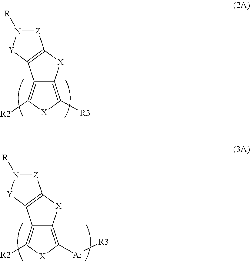

[Fifth and Sixth Polymers]


[Method for Synthesizing Organic High Molecular Compound]


R2-LR3-LR2—SnR″3R3—SnR″3


Q-Ar-Q (8)

[Solar Cell]
CH3NH4ML3. (28)
In the formula (28), M is at least one atom selected from a group consisting of lead (Pb) and tin (Sn), and L is at least one atom selected from a group consisting of iodine (I), bromine (Br), and chlorine (Cl).


(Synthesis of Compound MA2)


| TABLE 1 | |||
| Evaluation result of characteristic of organic thin film solar cell | |||
| Open circuit | Short-circuit | Power | Deterioration rate |
| voltage | current density | generation | Light | Heat | |||
| (Voc) | (Jsc) | Fill factor | efficiency | deterioration | deterioration | ||
| Polymer | [V] | [mA/cm2] | (FF) | [%] | [%] | [%] | |
| Example 9 | Example 1 [P1] | 0.94 | 13.5 | 0.61 | 7.74 | — | — |
| Example 10 | Example 2 [P2] | 0.91 | 12.3 | 0.60 | 6.72 | — | — |
| Example 11 | Example 3 [P3] | 0.96 | 12.8 | 0.59 | 7.25 | — | — |
| Example 12 | Example 4 [P4] | 0.93 | 11.8 | 0.58 | 6.36 | — | — |
| Example 13 | Example 5 [P5] | 0.94 | 12.5 | 0.58 | 6.82 | — | — |
| Example 14 | Example 6 [P6] | 0.92 | 12.1 | 0.59 | 6.57 | — | — |
| Example 15 | Example 7 [P7] | 0.96 | 11.8 | 0.57 | 6.46 | 13 | 28 |
| Example 16 | Example 8 [P8] | 0.96 | 12.3 | 0.58 | 6.85 | 11 | 27 |
| Example 17 | Example 7 [P7] + | 0.95 | 11.0 | 0.56 | 5.85 | 3 | 9 |
| photocross linking | |||||||
| Example 18 | Example 8 [P8] + | 0.95 | 11.2 | 0.56 | 5.96 | 3 | 8 |
| photocross linking | |||||||
| Comparative | P3HT | 0.56 | 8.5 | 0.60 | 2.86 | — | — |
| Example 1 | |||||||
| TABLE 2 | |||
| Evaluation result of characteristic | |||
| of organic thin film solar cell | |||
| Short-circuit | ||||||
| Open circuit | current | Power | ||||
| voltage | density | Fill | generation | Deterioration | ||
| (Voc) | (Jsc) | factor | efficiency | rate | ||
| Polymer | [V] | [mA/cm2] | (FF) | [%] | [%] | |
| Example 19 | Example 1 [P1] | 0.81 | 15.2 | 0.63 | 7.76 | 5 |
| Example 20 | Example 2 [P2] | 0.78 | 14.9 | 0.62 | 7.21 | 4 |
| Example 21 | Example 3 [P3] | 0.79 | 14.9 | 0.60 | 7.06 | 5 |
| Example 22 | Example 4 [P4] | 0.83 | 13.8 | 0.59 | 6.76 | 6 |
| Example 23 | Example 5 [P5] | 0.81 | 14.5 | 0.58 | 6.81 | 3 |
| Example 24 | Example 6 [P6] | 0.79 | 13.8 | 0.59 | 6.43 | 3 |
| Example 25 | Example 7 [P7] | 0.83 | 12.3 | 0.58 | 5.92 | 4 |
| Comparative | P3HT | 0.50 | 10.5 | 0.65 | 3.41 | 4 |
| Example 2 | ||||||
| Comparative | Spiro-OMeTAD + | 0.93 | 18.3 | 0.64 | 9.72 | 75 |
| Example 3 | Li-TFSI | |||||
Claims (12)


Applications Claiming Priority (2)
| Application Number | Priority Date | Filing Date | Title |
|---|---|---|---|
| JP2015-059411 | 2015-03-23 | ||
| JP2015059411A JP5957564B1 (en) | 2015-03-23 | 2015-03-23 | Polymer and solar cell using the same |
Publications (2)
| Publication Number | Publication Date |
|---|---|
| US20160285001A1 US20160285001A1 (en) | 2016-09-29 |
| US9634252B2 true US9634252B2 (en) | 2017-04-25 |
Family
ID=56513769
Family Applications (1)
| Application Number | Title | Priority Date | Filing Date |
|---|---|---|---|
| US15/072,834 Active US9634252B2 (en) | 2015-03-23 | 2016-03-17 | Polymer and solar cell using the same |
Country Status (2)
| Country | Link |
|---|---|
| US (1) | US9634252B2 (en) |
| JP (1) | JP5957564B1 (en) |
Families Citing this family (1)
| Publication number | Priority date | Publication date | Assignee | Title |
|---|---|---|---|---|
| KR20180074577A (en) * | 2016-12-23 | 2018-07-03 | 가부시키가이샤 한도오따이 에네루기 켄큐쇼 | Light-emitting element, light-emitting device, electronic device, display device, and lighting device |
Citations (6)
| Publication number | Priority date | Publication date | Assignee | Title |
|---|---|---|---|---|
| WO2010008672A1 (en) | 2008-07-18 | 2010-01-21 | University Of Chicago | Semiconducting polymers |
| WO2011011545A1 (en) | 2009-07-24 | 2011-01-27 | Solarmer Energy, Inc. | Conjugated polymers with carbonyl substituted thieno [3,4-b] thiophene units for polymer solar cell active layer materials |
| CA2727497A1 (en) | 2010-01-19 | 2011-07-19 | Xerox Corporation | Benzodithiophene based materials compositions |
| JP2012241016A (en) | 2011-05-13 | 2012-12-10 | Mitsubishi Chemicals Corp | Copolymer, organic semiconductor material, and organic electronic device, photoelectric transducer, and solar cell module using the organic semiconductor material |
| WO2013066065A1 (en) * | 2011-11-01 | 2013-05-10 | 경상대학교산학협력단 | Organic semiconductor compound, method for manufacturing same, and organic solar cell using same |
| WO2014208011A1 (en) | 2013-06-28 | 2014-12-31 | Kabushiki Kaisha Toshiba | Polymer and solar cell using the same |
-
2015
- 2015-03-23 JP JP2015059411A patent/JP5957564B1/en active Active
-
2016
- 2016-03-17 US US15/072,834 patent/US9634252B2/en active Active
Patent Citations (19)
| Publication number | Priority date | Publication date | Assignee | Title |
|---|---|---|---|---|
| WO2010008672A1 (en) | 2008-07-18 | 2010-01-21 | University Of Chicago | Semiconducting polymers |
| US20110124822A1 (en) | 2008-07-18 | 2011-05-26 | Luping Yu | Semiconducting polymers |
| US20140235817A1 (en) | 2008-07-18 | 2014-08-21 | University Of Chicago | Semiconducting polymers |
| US20140005347A1 (en) | 2008-07-18 | 2014-01-02 | University Of Chicago | Semiconducting polymers |
| WO2011011545A1 (en) | 2009-07-24 | 2011-01-27 | Solarmer Energy, Inc. | Conjugated polymers with carbonyl substituted thieno [3,4-b] thiophene units for polymer solar cell active layer materials |
| US20110017956A1 (en) | 2009-07-24 | 2011-01-27 | Solarmer Energy, Inc. | Conjugated polymers with carbonyl substituted thieno[3,4-b]thiophene units for polymer solar cell active layer materials |
| US20130123449A1 (en) | 2009-07-24 | 2013-05-16 | Solarmer Energy, Inc. | Conjugated polymers with carbonyl-substituted thieno [3,4-b] thiophene units for polymer solar cell active layer materials |
| GB2477194A (en) | 2010-01-19 | 2011-07-27 | Xerox Corp | Benzodithiophene based materials compositions |
| DE102011002579A1 (en) | 2010-01-19 | 2011-07-21 | Xerox Corporation Patent Documentation Center, N.Y. | Benzodithiophene-based material compositions |
| KR20110085911A (en) | 2010-01-19 | 2011-07-27 | 제록스 코포레이션 | Benzodithiophene based materials compositions |
| JP2011151396A (en) | 2010-01-19 | 2011-08-04 | Xerox Corp | Polymer semiconductor, method of manufacturing polymer semiconductor and electronic device |
| TW201134849A (en) | 2010-01-19 | 2011-10-16 | Xerox Corp | Benzodithiophene based materials compositions |
| US20110178255A1 (en) | 2010-01-19 | 2011-07-21 | Xerox Corporation | Benzodithiophene based materials compositions |
| CN102127210A (en) | 2010-01-19 | 2011-07-20 | 施乐公司 | Benzodithiophene based materials compositions |
| CA2727497A1 (en) | 2010-01-19 | 2011-07-19 | Xerox Corporation | Benzodithiophene based materials compositions |
| JP2012241016A (en) | 2011-05-13 | 2012-12-10 | Mitsubishi Chemicals Corp | Copolymer, organic semiconductor material, and organic electronic device, photoelectric transducer, and solar cell module using the organic semiconductor material |
| WO2013066065A1 (en) * | 2011-11-01 | 2013-05-10 | 경상대학교산학협력단 | Organic semiconductor compound, method for manufacturing same, and organic solar cell using same |
| WO2014208011A1 (en) | 2013-06-28 | 2014-12-31 | Kabushiki Kaisha Toshiba | Polymer and solar cell using the same |
| JP2015010173A (en) | 2013-06-28 | 2015-01-19 | 株式会社東芝 | Polymer and solar battery using the same |
Non-Patent Citations (3)
| Title |
|---|
| Jin Hyuck Heo, et al., "Efficient inorganic-organic hybrid heterojunction solar cells containing perovskite compound and polymeric hole conductors" Nature Photonics, vol. 7, Jun. 2013, pp. 486-491. |
| Mikkel Jørgensen, et al., "Stability of Polymer Solar Cells" Advanced Materials, vol. 24, 2012, pp. 580-612. |
| Seul-Ong Kim, et al., "N-Octyl-2,7-dithia-5-azacyclopenta[α]pentalene-4,6-dione-Based Low Band Gap Polymers for Efficient Solar Cells" Macromolecules, American Chemical Society, vol. 46, 2013, pp. 3861-3869. |
Also Published As
| Publication number | Publication date |
|---|---|
| JP2016176048A (en) | 2016-10-06 |
| US20160285001A1 (en) | 2016-09-29 |
| JP5957564B1 (en) | 2016-07-27 |
Similar Documents
| Publication | Publication Date | Title |
|---|---|---|
| Mo et al. | Chlorination of low-band-gap polymers: Toward high-performance polymer solar cells | |
| CN109891616B (en) | Organic semiconductor compound | |
| US10355212B2 (en) | Polymer and solar cell using the same | |
| Tamilavan et al. | Synthesis and characterization of indenofluorene‐based copolymers containing 2, 5‐bis (2‐thienyl)‐N‐arylpyrrole for bulk heterojunction solar cells and polymer light‐emitting diodes | |
| WO2013018951A1 (en) | Conductive polymer comprising 3,6-carbazole and organic solar cell using same | |
| US20180198068A1 (en) | Organic semiconducting compounds | |
| US11649321B2 (en) | Organic semiconducting compounds | |
| JP5898782B2 (en) | Polymer, organic thin-film solar cell using the same, and electronic device comprising the battery | |
| Lee et al. | Random copolymers based on 3‐hexylthiophene and benzothiadiazole with induced π‐conjugation length and enhanced open‐circuit voltage property for organic photovoltaics | |
| US9818945B2 (en) | Polymer and solar cell using the same | |
| JP6441196B2 (en) | Polymer and solar cell using the same | |
| US9634252B2 (en) | Polymer and solar cell using the same | |
| Li et al. | Molecular Engineering of Polymeric Hole-Transporting Materials for Efficient and Stable Perovskite Solar Cells | |
| US9905766B2 (en) | Polymer and solar cell using the same | |
| US9698349B2 (en) | Polymer and solar cell using the same | |
| WO2013118794A1 (en) | Organic thin film solar cell | |
| KR101564406B1 (en) | Novel Conjugated Polymer and Organo-Electronic Device Using the Same | |
| Fang et al. | Synthesis of a selenium and germanium containing random copolymer as an acceptor for all‐polymer solar cells | |
| KR101282062B1 (en) | Semiconductor polymers comprising a perylene moiety | |
| JP2024027112A (en) | Organic semiconductor polymers and organic optoelectronic devices containing them | |
| WO2018119780A1 (en) | Weak electron-donating building blocks, copolymers thereof and related devices | |
| JP2016184698A (en) | Photoelectric transducer, solar cell, and solar cell module |
Legal Events
| Date | Code | Title | Description |
|---|---|---|---|
| AS | Assignment |
Owner name: KABUSHIKI KAISHA TOSHIBA, JAPAN Free format text: ASSIGNMENT OF ASSIGNORS INTEREST;ASSIGNORS:NAKANO, YOSHIHIKO;MORI, SHIGEHIKO;GOTANDA, TAKESHI;AND OTHERS;SIGNING DATES FROM 20160328 TO 20160329;REEL/FRAME:038416/0357 |
|
| STCF | Information on status: patent grant |
Free format text: PATENTED CASE |
|
| MAFP | Maintenance fee payment |
Free format text: PAYMENT OF MAINTENANCE FEE, 4TH YEAR, LARGE ENTITY (ORIGINAL EVENT CODE: M1551); ENTITY STATUS OF PATENT OWNER: LARGE ENTITY Year of fee payment: 4 |
|
| MAFP | Maintenance fee payment |
Free format text: PAYMENT OF MAINTENANCE FEE, 8TH YEAR, LARGE ENTITY (ORIGINAL EVENT CODE: M1552); ENTITY STATUS OF PATENT OWNER: LARGE ENTITY Year of fee payment: 8 |