US11892726B2 - Image display method and image display device - Google Patents
Image display method and image display device Download PDFInfo
- Publication number
- US11892726B2 US11892726B2 US17/901,609 US202217901609A US11892726B2 US 11892726 B2 US11892726 B2 US 11892726B2 US 202217901609 A US202217901609 A US 202217901609A US 11892726 B2 US11892726 B2 US 11892726B2
- Authority
- US
- United States
- Prior art keywords
- areas
- light
- synchronization signal
- respect
- image display
- Prior art date
- Legal status (The legal status is an assumption and is not a legal conclusion. Google has not performed a legal analysis and makes no representation as to the accuracy of the status listed.)
- Active
Links
- 238000000034 method Methods 0.000 title claims abstract description 29
- 239000004973 liquid crystal related substance Substances 0.000 claims abstract description 108
- 230000003111 delayed effect Effects 0.000 claims abstract description 7
- 239000011159 matrix material Substances 0.000 claims description 25
- 230000000630 rising effect Effects 0.000 claims 8
- 235000019557 luminance Nutrition 0.000 description 43
- 238000006243 chemical reaction Methods 0.000 description 22
- 239000000758 substrate Substances 0.000 description 14
- 238000013500 data storage Methods 0.000 description 12
- 229920005989 resin Polymers 0.000 description 11
- 239000011347 resin Substances 0.000 description 11
- 238000000638 solvent extraction Methods 0.000 description 11
- 239000012790 adhesive layer Substances 0.000 description 10
- 230000008859 change Effects 0.000 description 10
- 230000002123 temporal effect Effects 0.000 description 10
- 239000003795 chemical substances by application Substances 0.000 description 7
- 238000010586 diagram Methods 0.000 description 6
- 230000004048 modification Effects 0.000 description 6
- 238000012986 modification Methods 0.000 description 6
- VYPSYNLAJGMNEJ-UHFFFAOYSA-N Silicium dioxide Chemical compound O=[Si]=O VYPSYNLAJGMNEJ-UHFFFAOYSA-N 0.000 description 4
- XLOMVQKBTHCTTD-UHFFFAOYSA-N Zinc monoxide Chemical compound [Zn]=O XLOMVQKBTHCTTD-UHFFFAOYSA-N 0.000 description 4
- 239000010410 layer Substances 0.000 description 4
- 230000003287 optical effect Effects 0.000 description 4
- 230000008569 process Effects 0.000 description 4
- 239000004065 semiconductor Substances 0.000 description 4
- GWEVSGVZZGPLCZ-UHFFFAOYSA-N Titan oxide Chemical compound O=[Ti]=O GWEVSGVZZGPLCZ-UHFFFAOYSA-N 0.000 description 3
- 229910052782 aluminium Inorganic materials 0.000 description 3
- 230000002349 favourable effect Effects 0.000 description 3
- 239000011521 glass Substances 0.000 description 3
- 239000000463 material Substances 0.000 description 3
- -1 polyethylene terephthalate Polymers 0.000 description 3
- 239000004925 Acrylic resin Substances 0.000 description 2
- 229920000178 Acrylic resin Polymers 0.000 description 2
- MCMNRKCIXSYSNV-UHFFFAOYSA-N Zirconium dioxide Chemical compound O=[Zr]=O MCMNRKCIXSYSNV-UHFFFAOYSA-N 0.000 description 2
- PNEYBMLMFCGWSK-UHFFFAOYSA-N aluminium oxide Inorganic materials [O-2].[O-2].[O-2].[Al+3].[Al+3] PNEYBMLMFCGWSK-UHFFFAOYSA-N 0.000 description 2
- TZCXTZWJZNENPQ-UHFFFAOYSA-L barium sulfate Chemical compound [Ba+2].[O-]S([O-])(=O)=O TZCXTZWJZNENPQ-UHFFFAOYSA-L 0.000 description 2
- 125000004122 cyclic group Chemical group 0.000 description 2
- 239000003822 epoxy resin Substances 0.000 description 2
- 230000006870 function Effects 0.000 description 2
- 229920000647 polyepoxide Polymers 0.000 description 2
- 229920000139 polyethylene terephthalate Polymers 0.000 description 2
- 239000005020 polyethylene terephthalate Substances 0.000 description 2
- 239000002096 quantum dot Substances 0.000 description 2
- 239000000377 silicon dioxide Substances 0.000 description 2
- 229920002050 silicone resin Polymers 0.000 description 2
- 239000000126 substance Substances 0.000 description 2
- 230000001360 synchronised effect Effects 0.000 description 2
- 229920005992 thermoplastic resin Polymers 0.000 description 2
- 229920001187 thermosetting polymer Polymers 0.000 description 2
- 239000011787 zinc oxide Substances 0.000 description 2
- 239000004593 Epoxy Substances 0.000 description 1
- 229910020440 K2SiF6 Inorganic materials 0.000 description 1
- NIXOWILDQLNWCW-UHFFFAOYSA-N acrylic acid group Chemical group C(C=C)(=O)O NIXOWILDQLNWCW-UHFFFAOYSA-N 0.000 description 1
- XAGFODPZIPBFFR-UHFFFAOYSA-N aluminium Chemical compound [Al] XAGFODPZIPBFFR-UHFFFAOYSA-N 0.000 description 1
- 229910002113 barium titanate Inorganic materials 0.000 description 1
- JRPBQTZRNDNNOP-UHFFFAOYSA-N barium titanate Chemical compound [Ba+2].[Ba+2].[O-][Ti]([O-])([O-])[O-] JRPBQTZRNDNNOP-UHFFFAOYSA-N 0.000 description 1
- 238000005452 bending Methods 0.000 description 1
- 230000008901 benefit Effects 0.000 description 1
- WUKWITHWXAAZEY-UHFFFAOYSA-L calcium difluoride Chemical compound [F-].[F-].[Ca+2] WUKWITHWXAAZEY-UHFFFAOYSA-L 0.000 description 1
- 229910001634 calcium fluoride Inorganic materials 0.000 description 1
- 238000009792 diffusion process Methods 0.000 description 1
- 230000000694 effects Effects 0.000 description 1
- 238000005516 engineering process Methods 0.000 description 1
- 239000000284 extract Substances 0.000 description 1
- 239000006260 foam Substances 0.000 description 1
- 229910052733 gallium Inorganic materials 0.000 description 1
- 230000007274 generation of a signal involved in cell-cell signaling Effects 0.000 description 1
- 230000005484 gravity Effects 0.000 description 1
- ORUIBWPALBXDOA-UHFFFAOYSA-L magnesium fluoride Chemical compound [F-].[F-].[Mg+2] ORUIBWPALBXDOA-UHFFFAOYSA-L 0.000 description 1
- 229910001635 magnesium fluoride Inorganic materials 0.000 description 1
- 239000000395 magnesium oxide Substances 0.000 description 1
- CPLXHLVBOLITMK-UHFFFAOYSA-N magnesium oxide Inorganic materials [Mg]=O CPLXHLVBOLITMK-UHFFFAOYSA-N 0.000 description 1
- AXZKOIWUVFPNLO-UHFFFAOYSA-N magnesium;oxygen(2-) Chemical compound [O-2].[Mg+2] AXZKOIWUVFPNLO-UHFFFAOYSA-N 0.000 description 1
- 229910052751 metal Inorganic materials 0.000 description 1
- 239000002184 metal Substances 0.000 description 1
- ZKATWMILCYLAPD-UHFFFAOYSA-N niobium pentoxide Inorganic materials O=[Nb](=O)O[Nb](=O)=O ZKATWMILCYLAPD-UHFFFAOYSA-N 0.000 description 1
- URLJKFSTXLNXLG-UHFFFAOYSA-N niobium(5+);oxygen(2-) Chemical compound [O-2].[O-2].[O-2].[O-2].[O-2].[Nb+5].[Nb+5] URLJKFSTXLNXLG-UHFFFAOYSA-N 0.000 description 1
- BPUBBGLMJRNUCC-UHFFFAOYSA-N oxygen(2-);tantalum(5+) Chemical compound [O-2].[O-2].[O-2].[O-2].[O-2].[Ta+5].[Ta+5] BPUBBGLMJRNUCC-UHFFFAOYSA-N 0.000 description 1
- 239000002245 particle Substances 0.000 description 1
- 229920000515 polycarbonate Polymers 0.000 description 1
- 239000004417 polycarbonate Substances 0.000 description 1
- 229920005668 polycarbonate resin Polymers 0.000 description 1
- 239000004431 polycarbonate resin Substances 0.000 description 1
- 229920000728 polyester Polymers 0.000 description 1
- 229920001225 polyester resin Polymers 0.000 description 1
- 239000004645 polyester resin Substances 0.000 description 1
- 229920000098 polyolefin Polymers 0.000 description 1
- 229920005672 polyolefin resin Polymers 0.000 description 1
- 229920001296 polysiloxane Polymers 0.000 description 1
- 229910052709 silver Inorganic materials 0.000 description 1
- 239000004332 silver Substances 0.000 description 1
- 239000002356 single layer Substances 0.000 description 1
- PBCFLUZVCVVTBY-UHFFFAOYSA-N tantalum pentoxide Inorganic materials O=[Ta](=O)O[Ta](=O)=O PBCFLUZVCVVTBY-UHFFFAOYSA-N 0.000 description 1
- OGIDPMRJRNCKJF-UHFFFAOYSA-N titanium oxide Inorganic materials [Ti]=O OGIDPMRJRNCKJF-UHFFFAOYSA-N 0.000 description 1
- 238000002834 transmittance Methods 0.000 description 1
- RUDFQVOCFDJEEF-UHFFFAOYSA-N yttrium(III) oxide Inorganic materials [O-2].[O-2].[O-2].[Y+3].[Y+3] RUDFQVOCFDJEEF-UHFFFAOYSA-N 0.000 description 1
Images


Classifications
-
- G—PHYSICS
- G09—EDUCATION; CRYPTOGRAPHY; DISPLAY; ADVERTISING; SEALS
- G09G—ARRANGEMENTS OR CIRCUITS FOR CONTROL OF INDICATING DEVICES USING STATIC MEANS TO PRESENT VARIABLE INFORMATION
- G09G3/00—Control arrangements or circuits, of interest only in connection with visual indicators other than cathode-ray tubes
- G09G3/20—Control arrangements or circuits, of interest only in connection with visual indicators other than cathode-ray tubes for presentation of an assembly of a number of characters, e.g. a page, by composing the assembly by combination of individual elements arranged in a matrix no fixed position being assigned to or needed to be assigned to the individual characters or partial characters
- G09G3/34—Control arrangements or circuits, of interest only in connection with visual indicators other than cathode-ray tubes for presentation of an assembly of a number of characters, e.g. a page, by composing the assembly by combination of individual elements arranged in a matrix no fixed position being assigned to or needed to be assigned to the individual characters or partial characters by control of light from an independent source
- G09G3/3406—Control of illumination source
- G09G3/342—Control of illumination source using several illumination sources separately controlled corresponding to different display panel areas, e.g. along one dimension such as lines
- G09G3/3426—Control of illumination source using several illumination sources separately controlled corresponding to different display panel areas, e.g. along one dimension such as lines the different display panel areas being distributed in two dimensions, e.g. matrix
-
- G—PHYSICS
- G02—OPTICS
- G02F—OPTICAL DEVICES OR ARRANGEMENTS FOR THE CONTROL OF LIGHT BY MODIFICATION OF THE OPTICAL PROPERTIES OF THE MEDIA OF THE ELEMENTS INVOLVED THEREIN; NON-LINEAR OPTICS; FREQUENCY-CHANGING OF LIGHT; OPTICAL LOGIC ELEMENTS; OPTICAL ANALOGUE/DIGITAL CONVERTERS
- G02F1/00—Devices or arrangements for the control of the intensity, colour, phase, polarisation or direction of light arriving from an independent light source, e.g. switching, gating or modulating; Non-linear optics
- G02F1/01—Devices or arrangements for the control of the intensity, colour, phase, polarisation or direction of light arriving from an independent light source, e.g. switching, gating or modulating; Non-linear optics for the control of the intensity, phase, polarisation or colour
- G02F1/13—Devices or arrangements for the control of the intensity, colour, phase, polarisation or direction of light arriving from an independent light source, e.g. switching, gating or modulating; Non-linear optics for the control of the intensity, phase, polarisation or colour based on liquid crystals, e.g. single liquid crystal display cells
- G02F1/133—Constructional arrangements; Operation of liquid crystal cells; Circuit arrangements
- G02F1/1333—Constructional arrangements; Manufacturing methods
- G02F1/1335—Structural association of cells with optical devices, e.g. polarisers or reflectors
- G02F1/1336—Illuminating devices
- G02F1/133602—Direct backlight
- G02F1/133603—Direct backlight with LEDs
-
- G—PHYSICS
- G09—EDUCATION; CRYPTOGRAPHY; DISPLAY; ADVERTISING; SEALS
- G09G—ARRANGEMENTS OR CIRCUITS FOR CONTROL OF INDICATING DEVICES USING STATIC MEANS TO PRESENT VARIABLE INFORMATION
- G09G3/00—Control arrangements or circuits, of interest only in connection with visual indicators other than cathode-ray tubes
- G09G3/20—Control arrangements or circuits, of interest only in connection with visual indicators other than cathode-ray tubes for presentation of an assembly of a number of characters, e.g. a page, by composing the assembly by combination of individual elements arranged in a matrix no fixed position being assigned to or needed to be assigned to the individual characters or partial characters
- G09G3/34—Control arrangements or circuits, of interest only in connection with visual indicators other than cathode-ray tubes for presentation of an assembly of a number of characters, e.g. a page, by composing the assembly by combination of individual elements arranged in a matrix no fixed position being assigned to or needed to be assigned to the individual characters or partial characters by control of light from an independent source
- G09G3/3406—Control of illumination source
-
- G—PHYSICS
- G09—EDUCATION; CRYPTOGRAPHY; DISPLAY; ADVERTISING; SEALS
- G09G—ARRANGEMENTS OR CIRCUITS FOR CONTROL OF INDICATING DEVICES USING STATIC MEANS TO PRESENT VARIABLE INFORMATION
- G09G3/00—Control arrangements or circuits, of interest only in connection with visual indicators other than cathode-ray tubes
- G09G3/20—Control arrangements or circuits, of interest only in connection with visual indicators other than cathode-ray tubes for presentation of an assembly of a number of characters, e.g. a page, by composing the assembly by combination of individual elements arranged in a matrix no fixed position being assigned to or needed to be assigned to the individual characters or partial characters
- G09G3/34—Control arrangements or circuits, of interest only in connection with visual indicators other than cathode-ray tubes for presentation of an assembly of a number of characters, e.g. a page, by composing the assembly by combination of individual elements arranged in a matrix no fixed position being assigned to or needed to be assigned to the individual characters or partial characters by control of light from an independent source
- G09G3/36—Control arrangements or circuits, of interest only in connection with visual indicators other than cathode-ray tubes for presentation of an assembly of a number of characters, e.g. a page, by composing the assembly by combination of individual elements arranged in a matrix no fixed position being assigned to or needed to be assigned to the individual characters or partial characters by control of light from an independent source using liquid crystals
-
- G—PHYSICS
- G02—OPTICS
- G02F—OPTICAL DEVICES OR ARRANGEMENTS FOR THE CONTROL OF LIGHT BY MODIFICATION OF THE OPTICAL PROPERTIES OF THE MEDIA OF THE ELEMENTS INVOLVED THEREIN; NON-LINEAR OPTICS; FREQUENCY-CHANGING OF LIGHT; OPTICAL LOGIC ELEMENTS; OPTICAL ANALOGUE/DIGITAL CONVERTERS
- G02F1/00—Devices or arrangements for the control of the intensity, colour, phase, polarisation or direction of light arriving from an independent light source, e.g. switching, gating or modulating; Non-linear optics
- G02F1/01—Devices or arrangements for the control of the intensity, colour, phase, polarisation or direction of light arriving from an independent light source, e.g. switching, gating or modulating; Non-linear optics for the control of the intensity, phase, polarisation or colour
- G02F1/13—Devices or arrangements for the control of the intensity, colour, phase, polarisation or direction of light arriving from an independent light source, e.g. switching, gating or modulating; Non-linear optics for the control of the intensity, phase, polarisation or colour based on liquid crystals, e.g. single liquid crystal display cells
- G02F1/133—Constructional arrangements; Operation of liquid crystal cells; Circuit arrangements
- G02F1/1333—Constructional arrangements; Manufacturing methods
- G02F1/1335—Structural association of cells with optical devices, e.g. polarisers or reflectors
- G02F1/1336—Illuminating devices
- G02F1/133601—Illuminating devices for spatial active dimming
-
- G—PHYSICS
- G02—OPTICS
- G02F—OPTICAL DEVICES OR ARRANGEMENTS FOR THE CONTROL OF LIGHT BY MODIFICATION OF THE OPTICAL PROPERTIES OF THE MEDIA OF THE ELEMENTS INVOLVED THEREIN; NON-LINEAR OPTICS; FREQUENCY-CHANGING OF LIGHT; OPTICAL LOGIC ELEMENTS; OPTICAL ANALOGUE/DIGITAL CONVERTERS
- G02F1/00—Devices or arrangements for the control of the intensity, colour, phase, polarisation or direction of light arriving from an independent light source, e.g. switching, gating or modulating; Non-linear optics
- G02F1/01—Devices or arrangements for the control of the intensity, colour, phase, polarisation or direction of light arriving from an independent light source, e.g. switching, gating or modulating; Non-linear optics for the control of the intensity, phase, polarisation or colour
- G02F1/13—Devices or arrangements for the control of the intensity, colour, phase, polarisation or direction of light arriving from an independent light source, e.g. switching, gating or modulating; Non-linear optics for the control of the intensity, phase, polarisation or colour based on liquid crystals, e.g. single liquid crystal display cells
- G02F1/133—Constructional arrangements; Operation of liquid crystal cells; Circuit arrangements
- G02F1/1333—Constructional arrangements; Manufacturing methods
- G02F1/1335—Structural association of cells with optical devices, e.g. polarisers or reflectors
- G02F1/1336—Illuminating devices
- G02F1/133602—Direct backlight
- G02F1/133605—Direct backlight including specially adapted reflectors
-
- G—PHYSICS
- G02—OPTICS
- G02F—OPTICAL DEVICES OR ARRANGEMENTS FOR THE CONTROL OF LIGHT BY MODIFICATION OF THE OPTICAL PROPERTIES OF THE MEDIA OF THE ELEMENTS INVOLVED THEREIN; NON-LINEAR OPTICS; FREQUENCY-CHANGING OF LIGHT; OPTICAL LOGIC ELEMENTS; OPTICAL ANALOGUE/DIGITAL CONVERTERS
- G02F1/00—Devices or arrangements for the control of the intensity, colour, phase, polarisation or direction of light arriving from an independent light source, e.g. switching, gating or modulating; Non-linear optics
- G02F1/01—Devices or arrangements for the control of the intensity, colour, phase, polarisation or direction of light arriving from an independent light source, e.g. switching, gating or modulating; Non-linear optics for the control of the intensity, phase, polarisation or colour
- G02F1/13—Devices or arrangements for the control of the intensity, colour, phase, polarisation or direction of light arriving from an independent light source, e.g. switching, gating or modulating; Non-linear optics for the control of the intensity, phase, polarisation or colour based on liquid crystals, e.g. single liquid crystal display cells
- G02F1/133—Constructional arrangements; Operation of liquid crystal cells; Circuit arrangements
- G02F1/1333—Constructional arrangements; Manufacturing methods
- G02F1/1335—Structural association of cells with optical devices, e.g. polarisers or reflectors
- G02F1/1336—Illuminating devices
- G02F1/133602—Direct backlight
- G02F1/133606—Direct backlight including a specially adapted diffusing, scattering or light controlling members
- G02F1/133607—Direct backlight including a specially adapted diffusing, scattering or light controlling members the light controlling member including light directing or refracting elements, e.g. prisms or lenses
-
- G—PHYSICS
- G02—OPTICS
- G02F—OPTICAL DEVICES OR ARRANGEMENTS FOR THE CONTROL OF LIGHT BY MODIFICATION OF THE OPTICAL PROPERTIES OF THE MEDIA OF THE ELEMENTS INVOLVED THEREIN; NON-LINEAR OPTICS; FREQUENCY-CHANGING OF LIGHT; OPTICAL LOGIC ELEMENTS; OPTICAL ANALOGUE/DIGITAL CONVERTERS
- G02F1/00—Devices or arrangements for the control of the intensity, colour, phase, polarisation or direction of light arriving from an independent light source, e.g. switching, gating or modulating; Non-linear optics
- G02F1/01—Devices or arrangements for the control of the intensity, colour, phase, polarisation or direction of light arriving from an independent light source, e.g. switching, gating or modulating; Non-linear optics for the control of the intensity, phase, polarisation or colour
- G02F1/13—Devices or arrangements for the control of the intensity, colour, phase, polarisation or direction of light arriving from an independent light source, e.g. switching, gating or modulating; Non-linear optics for the control of the intensity, phase, polarisation or colour based on liquid crystals, e.g. single liquid crystal display cells
- G02F1/133—Constructional arrangements; Operation of liquid crystal cells; Circuit arrangements
- G02F1/1333—Constructional arrangements; Manufacturing methods
- G02F1/1335—Structural association of cells with optical devices, e.g. polarisers or reflectors
- G02F1/1336—Illuminating devices
- G02F1/133614—Illuminating devices using photoluminescence, e.g. phosphors illuminated by UV or blue light
-
- G—PHYSICS
- G09—EDUCATION; CRYPTOGRAPHY; DISPLAY; ADVERTISING; SEALS
- G09G—ARRANGEMENTS OR CIRCUITS FOR CONTROL OF INDICATING DEVICES USING STATIC MEANS TO PRESENT VARIABLE INFORMATION
- G09G2310/00—Command of the display device
- G09G2310/02—Addressing, scanning or driving the display screen or processing steps related thereto
- G09G2310/024—Scrolling of light from the illumination source over the display in combination with the scanning of the display screen
-
- G—PHYSICS
- G09—EDUCATION; CRYPTOGRAPHY; DISPLAY; ADVERTISING; SEALS
- G09G—ARRANGEMENTS OR CIRCUITS FOR CONTROL OF INDICATING DEVICES USING STATIC MEANS TO PRESENT VARIABLE INFORMATION
- G09G2320/00—Control of display operating conditions
- G09G2320/02—Improving the quality of display appearance
- G09G2320/0261—Improving the quality of display appearance in the context of movement of objects on the screen or movement of the observer relative to the screen
-
- G—PHYSICS
- G09—EDUCATION; CRYPTOGRAPHY; DISPLAY; ADVERTISING; SEALS
- G09G—ARRANGEMENTS OR CIRCUITS FOR CONTROL OF INDICATING DEVICES USING STATIC MEANS TO PRESENT VARIABLE INFORMATION
- G09G2320/00—Control of display operating conditions
- G09G2320/06—Adjustment of display parameters
- G09G2320/0626—Adjustment of display parameters for control of overall brightness
- G09G2320/064—Adjustment of display parameters for control of overall brightness by time modulation of the brightness of the illumination source
-
- G—PHYSICS
- G09—EDUCATION; CRYPTOGRAPHY; DISPLAY; ADVERTISING; SEALS
- G09G—ARRANGEMENTS OR CIRCUITS FOR CONTROL OF INDICATING DEVICES USING STATIC MEANS TO PRESENT VARIABLE INFORMATION
- G09G2360/00—Aspects of the architecture of display systems
- G09G2360/16—Calculation or use of calculated indices related to luminance levels in display data
Definitions
- Embodiments relate to an image display method and an image display device.
- a conventionally-known image display device includes a backlight and a liquid crystal panel.
- the backlight includes multiple light-emitting regions arranged in a matrix configuration and in which light sources are located in the light-emitting regions.
- the liquid crystal panel is located above the backlight and includes multiple pixels.
- an image display method using an image display device includes a back light and a liquid crystal panel.
- the backlight has a plurality of light-emitting regions arranged in a matrix configuration in a first direction and a second direction.
- the light-emitting regions is divided into a plurality of first areas in the first direction.
- the liquid crystal panel is on the backlight.
- the liquid crystal panel has a plurality of pixels arranged in a matrix configuration in the first and second directions.
- the pixels are divided into a plurality of second areas in the first direction.
- a first operation to cause light to be emitted from the light-emitting regions at respective intensity in accordance with frame image data is performed sequentially with respect to each of the first areas.
- a second operation to apply voltages to the pixels at respective levels in accordance with the frame image data is performed sequentially with respect to each of the second areas.
- a timing at which the first operation with respect to each of the first areas is started is delayed from a timing at which the second operation with respect to a corresponding one of the second areas is started by a predetermined interval.
- an image display device includes a back light, a liquid crystal panel, and a controller.
- the backlight includes a plurality of light-emitting regions arranged in a matrix configuration in a first direction and a second direction. The light-emitting regions are divided into a plurality of first areas in the first direction.
- the liquid crystal panel is on the backlight.
- the liquid crystal panel includes a plurality of pixels arranged in a matrix configuration in the first and second directions. The pixels are divided into a plurality of second areas in the first direction.
- the controller is configured to perform a first operation to cause light to be emitted from the light-emitting regions at respective intensity corresponding to frame image data, sequentially with respect to each of the first areas, and a second operation to apply voltages to the pixels at respective levels corresponding to the frame image data, sequentially with respect to each of the second areas.
- a timing at which the controller starts the first operation with respect to each of the first areas is delayed from a timing at which the controller starts the second operation with respect to a corresponding one of the second areas by a predetermined interval.
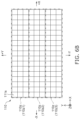
- FIG. 1 illustrates an exploded perspective view of an image display device according to an embodiment.
- FIG. 2 illustrates a top view of a planar light source of a backlight of the image display device according to the embodiment.
- FIG. 3 illustrates a cross-sectional view of the planar light source along line in FIG. 2 .
- FIG. 4 illustrates a top view of a liquid crystal panel of the image display device according to the embodiment.
- FIG. 5 is a block diagram showing components of the image display device according to the embodiment.
- FIG. 6 A schematically illustrates a relationship among pixels of an input image, a light-emitting regions of the backlight, and pixels of the liquid crystal panel according to the embodiment.
- FIG. 6 B schematically illustrates areas of the backlight of which outputs are simultaneously controlled according to the embodiment.
- FIG. 6 C schematically illustrates areas of the liquid crystal panel of which gradations are simultaneously controlled according to the embodiment.
- FIG. 7 is a diagram to explain a method for generating luminance setting data.
- FIG. 8 is a diagram to explain a method for generating gradation setting data.
- FIG. 9 A is a timing chart schematically illustrating a temporal change of a synchronization signal according to the embodiment.
- FIG. 9 B is a timing chart schematically illustrating a temporal change of potential of a pixel belonging to an upper area of the liquid crystal panel according to the embodiment.
- FIG. 9 C is a timing chart schematically illustrating a temporal change of potential of a pixel belonging to a middle area of the liquid crystal panel according to the embodiment.
- FIG. 9 D is a timing chart schematically illustrating a temporal change of potential of a pixel belonging to a lower area of the liquid crystal panel according to the embodiment.
- FIG. 9 E is a timing chart schematically illustrating timing of a backlight driver receiving a control signal according to the embodiment.
- FIG. 9 F is a timing chart schematically illustrating a temporal change of a sub-synchronization signal according to the embodiment.
- FIG. 9 G is a timing chart schematically illustrating timing of controlling output of a light source belonging to the upper area of the backlight according to the embodiment.
- FIG. 9 H is a timing chart schematically illustrating timing of controlling output of a light source belonging to the middle area of the backlight according to the embodiment.
- FIG. 9 I is a timing chart schematically illustrating timing of controlling output of a light source belonging to the lower area of the backlight according to the embodiment.
- FIG. 10 A illustrates a top view of a modification of the planar light source.
- FIG. 10 B illustrates a cross-sectional view of the planar light source along line XB-XB in FIG. 10 A .
- X-axis, Y-axis, and Z-axis are orthogonal to each other.
- the direction in which the X-axis extends is referred to as an “X-direction”; the direction in which the Y-axis extends is referred to as a “Y-direction”; and the direction in which the Z-axis extends is referred to as a “Z-direction”.
- X-direction The direction in which the X-axis extends
- Y-direction the direction in which the Y-axis extends
- Z-direction the direction in which the Z-axis extends
- the Z-direction that is from the backlight toward the liquid crystal panel is referred to as “up” and the opposite direction is referred to as “down”, these directions are independent of the direction of gravity.
- one direction in which the X-axis extends in the drawings is called the “+X direction”; and the opposite direction is called the “ ⁇ X direction”.
- one direction in which the Y-axis extends is called the “+Y direction”; and the opposite direction is called the “ ⁇ Y direction”.
- FIG. 1 illustrates an exploded perspective view of an image display device according to an embodiment.
- the image display device 100 is, for example, a liquid crystal module (LCM) used in a display of an external device (not illustrated) such as a television, a personal computer, a game machine, etc.
- the image display device 100 includes a backlight 110 , a liquid crystal panel 120 , and a controller 130 .
- the controller 130 includes a timing controller 140 , a driver 150 for the backlight 110 , and a driver 160 for the liquid crystal panel 120 .
- Components of the image display device 100 will now be described. For easier understanding of the description, electrical connections between the components are shown by connecting the components to each other with solid lines in FIG. 1 .
- the backlight 110 is drivable by local dimming.
- the backlight 110 includes a planar light source 111 , and an optical member 112 located on the planar light source 111 .
- the optical member 112 is, for example, a sheet or a plate that has a light-modulating function such as light diffusion, etc. According to the embodiment, the number of the optical members 112 included in the backlight 110 is one. Alternatively, the number of optical members included in the backlight may be two or more.
- FIG. 2 illustrates a top view of the planar light source of the backlight of the image display device according to the embodiment.
- FIG. 3 illustrates a cross-sectional view of the planar light source along line in FIG. 2 .
- the planar light source 111 includes a substrate 113 , a light-reflective sheet 114 , a light guide member 115 , multiple light sources 116 , a light-transmitting member 117 , a first light-modulating member 118 , and a light-reflecting member 119 .
- the substrate 113 is a wiring substrate that includes an insulating member and multiple wirings located on the insulating member.
- the shape of the substrate 113 when viewed in top-view is substantially rectangular as shown in FIG. 2 .
- the shape of the substrate is not limited to such a shape.
- the upper surface and the lower surface of the substrate 113 are flat surfaces and are substantially parallel to the X-direction and the Y-direction (i.e., the XY plane).
- the light-reflective sheet 114 is located on the substrate 113 .
- the light-reflective sheet 114 includes, for example, a first adhesive layer 114 a , a light-reflecting layer 114 b located on the first adhesive layer 114 a , and a second adhesive layer 114 c located on the light-reflecting layer 114 b .
- the light-reflective sheet 114 is adhered to the substrate 113 with the first adhesive layer 114 a .
- a resin that includes many bubbles can be used as the light-reflecting layer 114 b .
- the first adhesive layer 114 a and the second adhesive layer 114 c can include, for example, a light-diffusing agent.
- the concentration of the light-diffusing agent included in the second adhesive layer 114 c is less than the concentration of the light-diffusing agent included in the first adhesive layer 114 a to reduce uneven luminance of light-emitting regions 111 s described below.
- the light-diffusing agent can be selected from light-diffusing agents included in a second light-modulating member 116 c and a third light-modulating member 116 d described below.
- the light guide member 115 is located on the light-reflective sheet 114 .
- the light guide member 115 is adhered to the light-reflective sheet 114 with the second adhesive layer 114 c .
- the light guide member 115 is plate-shaped. However, the shape of the light guide member is not limited to such a shape. It is favorable for the thickness of the light guide member 115 to be not less than 200 ⁇ m and not more than 800 ⁇ m.
- the light guide member 115 may be a single layer or may include a stacked body of multiple layers.
- thermoplastic resin such as acrylic, polycarbonate, cyclic polyolefin, polyethylene terephthalate, polyester, or the like, a thermosetting resin such as epoxy, silicone, or the like, glass, etc., are examples of materials included in the light guide member 115 .
- Multiple light source placement portions 115 a are located in the light guide member 115 . As shown in FIG. 2 , the multiple light source placement portions 115 a are arranged in a matrix configuration when viewed in top-view. As shown in FIG. 3 , each light source placement portion 115 a is a through-hole that extends through the light guide member 115 in the Z-direction. Alternatively, the light source placement portion may be a recess located at the lower surface of the light guide member.
- the light sources 116 are located in the light source placement portions 115 a , respectively. Accordingly, as shown in FIG. 2 , the multiple light sources 116 also are arranged in a matrix configuration. Alternatively, the light sources 116 may be embedded in the light guide member 115 without providing light source placement portions in the light guide member 115 . Also, it is not always necessary for the light guide member 115 to be included in the planar light source 111 . For example, the planar light source 111 may include no light guide member, and the multiple light sources 116 may be simply arranged in a matrix configuration on the substrate 113 .
- each light source 116 is a light-emitting device in which a wavelength conversion member 116 b is coupled to a light-emitting element 116 a .
- Each light source 116 further includes the second light-modulating member 116 c and the third light-modulating member 116 d .
- each light source may be a solitary light-emitting element instead of a light-emitting device.
- the light-emitting element 116 a is, for example, an LED (Light-Emitting Diode).
- the light-emitting element 116 a includes a semiconductor stacked body 116 e and a pair of electrodes 116 f and 116 g that electrically connects the semiconductor stacked body 116 e and the wiring of the substrate 113 .
- Through-holes are located in portions of the light-reflective sheet 114 positioned directly under the electrodes 116 f and 116 g .
- Conductive members 113 m that electrically connect the wiring of the substrate 113 and the electrodes 116 f and 116 g are located in the through-holes.
- the wavelength conversion member 116 b includes a light-transmitting member 116 h that covers the upper surface and the side surface of the semiconductor stacked body 116 e , and a wavelength conversion substance 116 i that is located in the light-transmitting member 116 h and converts the wavelength of the light emitted by the semiconductor stacked body 116 e into a different wavelength.
- the wavelength conversion substance 116 i is, for example, a fluorescer.
- the light-emitting element 116 a emits blue light.
- the wavelength conversion member 116 b includes a fluorescer that generates red light and a fluorescer that generates green light.
- a fluorescer that generates red light is called a “red fluorescer”
- a fluorescer that generates green light is called a “green fluorescer”.
- a CASN-based fluorescer e.g., CaAlSiN 3 :Eu
- a KSF-based fluorescer e.g., K 2 SiF 6 :Mn
- a KSAF-based fluorescer e.g., K 2 [Si p Al q Mn r F s ] (0.9 ⁇ p+q+r ⁇ 1.1, 0 ⁇ q ⁇ 0.1, 0 ⁇ r ⁇ 0.2, and 5.9 ⁇ s ⁇ 6.1)
- a quantum dot fluorescer e.g., Ag p Cu 1-p In q Ga 1-q S 2 (0 ⁇ p ⁇ 1 and 0 ⁇ q ⁇ 1)
- the red fluorescer e.g., Ag p Cu 1-p In q Ga 1-q S 2
- a fluorescer that has a perovskite structure (e.g., CsPb(F, Cl, Br, I) 3 ), a ⁇ -sialon-based fluorescer (e.g., (Si, Al) 3 (O, N) 4 :Eu), a LAG-based fluorescer (e.g., Lu 3 (Al, Ga) 5 O 12 :Ce), or a quantum dot fluorescer (e.g., AgIn p Ga 1-p S 2 (0 ⁇ p ⁇ 1)) are examples of the green fluorescer.
- the backlight 110 can emit white light that is composed of the blue light emitted by the light-emitting element 116 a and the red and green light generated by the wavelength conversion member 116 b.
- the wavelength conversion member 116 b may be a light-transmitting member that does not include a fluorescer.
- the light source is a solitary light-emitting element as described above, for example, similar white light can be obtained by providing a fluorescer sheet including a red fluorescer and a green fluorescer on the planar light source or by providing a fluorescer sheet including a red fluorescer and a fluorescer sheet including a green fluorescer on the planar light source.
- the second light-modulating member 116 c covers the upper surface of the wavelength conversion member 116 b .
- the second light-modulating member 116 c can control the amount and/or emission direction of the light emitted from the upper surface of the wavelength conversion member 116 b.
- the third light-modulating member 116 d covers the lower surface of the light-emitting element 116 a and the lower surface of the wavelength conversion member 116 b so that the lower surfaces of the electrodes 116 f and 116 g are exposed.
- the third light-modulating member 116 d can reflect the light toward the lower surface of the wavelength conversion member 116 b to control the light to be emitted from the upper surface and the side surface of the wavelength conversion member 116 b.
- the second light-modulating member 116 c and the third light-modulating member 116 d each can include a light-transmitting resin, and a light-diffusing agent included in the light-transmitting resin.
- a silicone resin, an epoxy resin, or an acrylic resin are examples of the light-transmitting resin.
- particles of titania, silica, alumina, zinc oxide, magnesium oxide, zirconia, yttria, calcium fluoride, magnesium fluoride, niobium pentoxide, barium titanate, tantalum pentoxide, barium sulfate, glass, etc. are examples of the light-diffusing agent.
- the second light-modulating member 116 c may also include a metal member such as, for example, aluminum, silver, etc., so that the luminance directly above the light source 116 does not become too high.
- the light-transmitting member 117 is located in the light source placement portion 115 a .
- the light-transmitting member 117 covers the light source 116 .
- the first light-modulating member 118 is located on the light-transmitting member 117 .
- the first light-modulating member 118 can reflect a portion of the light incident from the light-transmitting member 117 and can transmit another portion of the light so that the luminance directly above the light source 116 does not become too high. It is favorable for the first light-modulating member 118 to cover the interface between the light-transmitting member 117 and the light guide member 115 when viewed in top-view so that locally high luminance due to scattering of the light from the light source 116 at the interface between the light-transmitting member 117 and the light guide member 115 can be suppressed.
- the first light-modulating member 118 can include a member similar to the second or third light-modulating member 116 c or 116 d.
- a partitioning trench 115 b is provided in the light guide member 115 to surround the light source placement portions 115 a when viewed in top-view.
- the partitioning trench 115 b has a lattice shape and extends in the X-direction and the Y-direction.
- the partitioning trench 115 b extends through the light guide member 115 in the Z-direction.
- the partitioning trench 115 b may be a recess provided in the upper or lower surface of the light guide member 115 .
- the partitioning trench 115 b may not be provided in the light guide member 115 .
- the light-reflecting member 119 is located in the partitioning trench 115 b .
- the light-reflecting member 119 can include, for example, a member similar to the second or third light-modulating member 116 c or 116 d .
- the light-reflecting member 119 covers a portion of the side surface of the partitioning trench 115 b in a layer shape.
- the light-reflecting member 119 may extend to cover the light-reflective sheet 114 exposed in the partitioning trench 115 b , and particularly the upper surface of the second adhesive layer 114 c so that the light from the light source 116 can be partitioned for each of the light-emitting regions 111 s described below.
- the light-reflecting member 119 may fill the entire interior of the partitioning trench 115 b .
- the light-reflecting member 119 may not be located in the partitioning trench 115 b.
- the outputs of the multiple light sources 116 are individually controllable by the backlight driver 150 .
- “controllable output” means that switching between a lit state and an unlit state is possible, and the luminance in the lit state is adjustable.
- the regions when viewed in the top-view of the planar light source 111 when subdivided into regions that include the light sources 116 of which outputs are individually controlled are called the “light-emitting regions 111 s ”.
- the light-emitting region 111 s corresponds to the minimum region of the planar light source 111 of which luminance is controlled by local dimming.
- the light-emitting regions 111 s correspond to regions when the planar light source 111 is partitioned into a lattice shape similarly to the partitioning trench 115 b . Therefore, each light-emitting region 111 s is rectangular as shown in FIG. 2 .
- One light source 116 is located in one light-emitting region 111 s .
- multiple light source groups may be arranged in a matrix configuration in the planar light source; and the output of each light source group may be controlled. In such a case, one light source group, i.e., a plurality of light sources, is located in one light-emitting region.
- the multiple light-emitting regions 111 s are arranged in a matrix configuration when viewed in top-view.
- a matrix configuration such as that of the multiple light-emitting regions 111 s
- an element group of the matrix of the light-emitting regions 111 s and the like arranged in the X-direction is called a “row”
- an element group of the matrix of the light-emitting regions 111 s and the like arranged in the Y-direction is called a “column”.
- the row that is positioned furthest toward the +Y side the left side of FIG.
- the multiple light-emitting regions 111 s are arranged in N1 rows and M1 columns.
- N1 and M1 each are any integer; and an example is shown in FIG. 2 in which N1 is 9 and M1 is 16.
- FIG. 4 illustrates a top view of the liquid crystal panel 120 of the image display device 100 according to the embodiment.
- the liquid crystal panel 120 is located on the backlight 110 .
- the liquid crystal panel 120 is substantially rectangular when viewed in top-view.
- the shape of the liquid crystal panel is not limited to such a shape.
- the liquid crystal panel 120 includes multiple pixels 120 p arranged in a matrix configuration. In FIG. 4 , one region that is surrounded with a fine double dot-dash line corresponds to one pixel 120 p.
- the liquid crystal panel 120 can display a color image.
- one pixel 120 p includes three subpixels 120 sp : a subpixel that can transmit blue light, a subpixel that can transmit green light, and a subpixel that can transmit red light when white light emitted from the backlight 110 is incident.
- the light transmittances of the subpixels 120 sp are individually controllable by the liquid crystal panel driver 160 .
- the gradations of the subpixels 120 sp are individually controlled thereby.
- the multiple pixels 120 p are arranged in N2 rows and M2 columns.
- N2 and M2 each are any integer such that N2>N1 and M2>M1.
- the multiple pixels 120 p are located in the light-emitting regions 111 s when viewed in top-view. Although an example is shown in FIG. 4 in which four pixels 120 p are located in each light-emitting region 111 s when viewed in top-view, the number of pixels of the liquid crystal panel located in each light-emitting region may be more or less than four.
- FIG. 5 is a block diagram showing components of the image display device according to the embodiment.
- FIG. 6 A schematically illustrate the relationship among the pixels of the input image, the light-emitting regions of the backlight, and the pixels of the liquid crystal panel according to the embodiment.
- FIG. 6 B schematically illustrates areas of the backlight of which outputs are simultaneously controlled according to the embodiment.
- FIG. 6 C schematically illustrate areas of the liquid crystal panel of which gradations are simultaneously controlled according to the embodiment.
- FIG. 7 is a diagram to explain a method for generating luminance setting data.
- FIG. 8 is a diagram to explain a method for generating gradation setting data.
- FIG. 9 A is a timing chart schematically illustrating the temporal change of a synchronization signal according to the embodiment.
- FIG. 9 B is a timing chart schematically illustrating the temporal change of the potential of a pixel belonging to the upper area of the liquid crystal panel according to the embodiment.
- FIG. 9 C is a timing chart schematic ally illustrating the temporal change of the potential of a pixel belonging to the middle area of the liquid crystal panel according to the embodiment.
- FIG. 9 D is a timing chart schematic ally illustrating the temporal change of the potential of a pixel belonging to the lower area of the liquid crystal panel according to the embodiment.
- FIG. 9 E is a timing chart schematic ally illustrating the timing of the backlight driver receiving the control signal according to the embodiment.
- FIG. 9 F is a timing chart schematic ally illustrating the temporal change of a sub-synchronization signal according to the embodiment.
- FIG. 9 G is a timing chart schematic ally illustrating the timing of controlling the output of a light source belonging to the upper area of the backlight according to the embodiment.
- FIG. 9 H is a timing chart schematic ally illustrating the timing of controlling the output of a light source belonging to the middle area of the backlight according to the embodiment.
- FIG. 9 I is a timing chart schematic ally illustrating the timing of controlling the output of a light source belonging to the lower area of the backlight according to the embodiment.
- the timing controller 140 is connected to an external device. Also, as shown in FIG. 5 , the timing controller 140 is connected to the backlight driver 150 and the liquid crystal panel driver 160 .
- the timing controller 140 includes an input module 141 , a luminance setting data generator 142 , a gradation setting data generator 143 , memory 144 , a sub-synchronization signal generator 145 , a control signal generator 146 , and an output module 147 .
- the input module 141 includes, for example, an input interface connected to the external device.
- the input module 141 accepts inputs of a synchronization signal 920 and the multiple input images 910 from the external device.
- each input image 910 includes multiple pixels 910 p arranged in a matrix configuration.
- an XY orthogonal coordinate system is used to represent the arrangement directions of the elements in data such as the input image 910 in which elements such as the pixels 910 p , etc., are arranged in a matrix configuration.
- one pixel 910 p of the input image 910 corresponds to one pixel 120 p of the liquid crystal panel 120 .
- the multiple pixels 910 p are arranged in N2 rows and M2 columns.
- four pixels 910 p are included in an image area 910 a corresponding to one light-emitting region 111 s of the backlight 110 .
- the correspondence between the pixels of the input image 910 and the pixels of the liquid crystal panel 120 may not be one-to-one.
- the number of pixels 910 p of the input image 910 corresponding to each light-emitting region 111 s may be more or less than four.
- the gradation is set for each pixel 910 p .
- the input image 910 is a color image.
- a blue gradation Gb, a green gradation Gg, and a red gradation Gr are set for each pixel 910 p .
- each of the gradations Gb, Gg, and Gr is a numeral that is not less than 0 and not more than 255 when represented using 8 bits.
- the synchronization signal 920 is a signal that indicates the timing of switching the input image 910 displayed in the liquid crystal panel 120 . As shown in FIG. 9 A , the synchronization signal 920 is a pulse signal, e.g., a vertical synchronization signal.
- the luminance setting data generator 142 uses each input image 910 to generate luminance setting data D 1 including setting values of the luminances of the light sources 116 of the backlight 110 .
- the luminance setting data generator 142 extracts a maximum value Gmax(i, j) of the gradations of the multiple pixels 910 p in the image area 910 a of the input image 910 corresponding to the light-emitting region 111 s positioned at the ith row and the jth column.
- i is an integer that is not less than 1 and not more than N1
- j is an integer that is not less than 1 and not more than M1.
- the luminance setting data generator 142 converts the extracted maximum value Gmax(i, j) of the gradations into a luminance e 1 ( i, j ).
- the luminance setting data generator 142 uses the luminance e 1 ( i, j ) as the value of the element at the ith row and the jth column of the luminance setting data D 1 .
- the luminance setting data generator 142 performs this processing for all of the light-emitting regions 111 s.
- the luminance setting data D 1 thus obtained is data of a matrix configuration that includes N1 rows and M1 columns.
- the value of the element of the luminance setting data D 1 at the ith row and the jth column is the setting value of the luminance of the light-emitting region 111 s positioned at the ith row and the jth column.
- the method for generating the luminance setting data is not limited to that described above.
- the gradation setting data generator 143 uses the luminance setting data D 1 , a luminance profile D 3 , and each input image 910 to generate gradation setting data D 2 including setting values of the gradations of the pixels 120 p of the liquid crystal panel 120 .
- the luminance profile D 3 is data that shows the luminance distribution at each position on the XY plane when the light source 116 of one light-emitting region 111 s is lit.
- ON means that the light source 116 of the light-emitting region 111 s is lit; and OFF means that the light source 116 of the light-emitting region 111 s is unlit.
- the gradation setting data generator 143 estimates a luminance value V(n, m) directly under the pixel 120 p positioned at the nth row and the mth column of the liquid crystal panel 120 from the luminance setting data D 1 and the luminance profile D 3 by including both the luminance distribution in one light-emitting region 111 s and the light leakage from the light-emitting regions 111 s at the periphery.
- n is an integer that is not less than 1 and not more than N2
- m is an integer that is not less than 1 and not more than M2.
- the gradation setting data generator 143 substitutes the estimated luminance value V(n, m) and the blue gradation Gb of the pixel 910 p corresponding to the pixel 120 p of the input image 910 in a conversion formula Ef.
- the conversion formula Ef is, for example, a conversion formula that converts the luminance into the gradation based on gamma correction.
- An output value Efb of the conversion formula Ef obtained by substituting the blue gradation Gb in the conversion formula Ef is used by the gradation setting data generator 143 as the setting value of the blue gradation of the pixel 120 p .
- Similar processing is performed also for the green gradation Gg; and an output value Efg of the conversion formula Ef obtained thereby is used as the setting value of the green gradation of the pixel 120 p .
- the gradation setting data generator 143 performs similar processing also for the red gradation Gr; and an output value Efr of the conversion formula Ef obtained thereby is used as the setting value of the red gradation of the pixel 120 p .
- the gradation setting data generator 143 uses the output values Efb, Efg, and Efr of the conversion formula Ef as the value of an element e 2 ( n, m ) at the nth row and the mth column of the gradation setting data D 2 .
- the gradation setting data generator 143 performs this processing for all of the pixels 120 p of the liquid crystal panel 120 .
- the gradation setting data D 2 thus obtained is data of a matrix configuration of N2 rows and M2 columns.
- the three values Efb, Efg, and Efr of the element e 2 ( n, m ) at the nth row and the mth column of the gradation setting data D 2 correspond respectively to the setting value of the blue gradation, the setting value of the green gradation, and the setting value of the red gradation of the pixel 120 p positioned at the nth row and the mth column of the liquid crystal panel 120 .
- the method for generating the gradation setting data is not limited to that described above.
- the luminance setting data generator 142 and the gradation setting data generator 143 include, for example, a processor such as a CPU (Central Processing Unit), etc.
- a processor such as a CPU (Central Processing Unit), etc.
- the memory 144 stores various data and various programs necessary for controlling the backlight 110 and the liquid crystal panel 120 such as the input image 910 , the luminance setting data D 1 , the gradation setting data D 2 , the luminance profile D 3 , etc.
- the memory 144 includes, for example, ROM (Read-Only Memory) and RAM (Random-Access Memory).
- the sub-synchronization signal generator 145 uses the synchronization signal 920 to generate a sub-synchronization signal 930 .
- the sub-synchronization signal 930 is a signal that indicates the timing of switching areas 110 z of the backlight 110 of which outputs are controlled by the backlight driver 150 .
- the sub-synchronization signal 930 is, for example, a pulse signal.
- the sub-synchronization signal 930 is synchronous with the synchronization signal 920 ; and multiple pulses of the sub-synchronization signal 930 are included in one period T of the synchronization signal 920 .
- an example is shown in which three pulses of the sub-synchronization signal 930 are included in one period T.
- the sub-synchronization signal generator 145 includes, for example, a generation circuit of a pulse signal.
- the control signal generator 146 generates a control signal D 1 a of the backlight 110 based on the luminance setting data D 1 .
- the control signal D 1 a is, for example, a PWM (Pulse Width Modulation) signal.
- the control signal generator 146 includes, for example, a PWM signal generation circuit.
- the output module 147 includes an output interface connected to the backlight 110 , an output interface connected to the liquid crystal panel 120 , etc. As shown in FIG. 5 , the output module 147 outputs the sub-synchronization signal 930 and the control signal D 1 a of the backlight 110 to the backlight driver 150 . Also, the output module 147 outputs the gradation setting data D 2 to the liquid crystal panel driver 160 as a control signal D 2 a of the liquid crystal panel 120 . The output module 147 also outputs the synchronization signal 920 to the liquid crystal panel driver 160 .
- the control signal generator 146 may convert the gradation setting data D 1 into a control signal of the liquid crystal panel 110 ; and the output module 147 may output the control signal to the liquid crystal panel 110 .
- the backlight driver 150 includes a data storage 151 , a driver 152 , an area switcher 153 , and a timing adjuster 154 .
- the data storage 151 stores the control signal D 1 a of the backlight 110 .
- the data storage 151 includes, for example, a latch circuit that can store the control signal D 1 a of the backlight 110 .
- the backlight 110 can be divided into the multiple areas 110 z arranged in the ⁇ Y direction as shown in FIG. 6 B . At least one row of the light-emitting regions 111 s is included in each area 110 z .
- FIG. 6 B shows an example in which the backlight 110 is divided into three areas 110 z ; and three rows of the light-emitting regions 111 s are included in each area 110 z .
- the area 110 z among the three areas 110 z that is positioned furthest toward the +Y side also is called an “upper area 110 z 1 ”; the area 110 z positioned at the ⁇ Y side of the upper area 110 z 1 also is called a “middle area 110 z 2 ”; and the area 110 z positioned at the ⁇ Y side of the middle area 110 z 2 also is called a “lower area 110 z 3 ”.
- the number of areas of the backlight and the number of light-emitting regions included in each area are not limited to such numbers.
- the number of areas of the backlight may be four or more.
- the driver 152 can simultaneously drive the light sources 116 in one area 110 z .
- the driver 152 includes, for example, a drive circuit of the multiple light sources 116 .
- the area switcher 153 switches the area 110 z that is driven by the driver 152 sequentially in the ⁇ Y direction at the timing of the rise of the sub-synchronization signal 930 .
- the area switcher 153 is connected between the driver 152 and the backlight 110 and includes a switch element that can switch the area 110 z driven by the driver 152 .
- a series of processing of switching the outputs of the light sources 116 of the light-emitting regions 111 s of the backlight 110 sequentially in the ⁇ Y direction for each of the areas 110 z is called “the processing of switching the outputs of the light sources 116 of the light-emitting regions 111 s”.
- the timing adjuster 154 adjusts the timing of transmitting the control signal D 1 a from the data storage 151 to the driver 152 .
- the timing adjuster 154 includes, for example, a shift register circuit connected between the data storage 151 and the driver 152 . The functions of the timing adjuster 154 are described below.
- the liquid crystal panel driver 160 includes a drive circuit of the liquid crystal panel 120 , etc.
- the liquid crystal panel 120 can be divided into multiple areas 120 z arranged in the ⁇ Y direction as shown in FIG. 6 C .
- Each area 120 z includes one row of the pixels 120 p .
- the portion of the liquid crystal panel 120 positioned directly above the upper area 110 z 1 of the backlight 110 is called an “upper portion 121 ”.
- the portion of the liquid crystal panel 120 positioned directly above the middle area 110 z 2 of the backlight 110 is called a “middle portion 122 ”.
- the portion of the liquid crystal panel 120 positioned directly above the lower area 110 z 3 of the backlight 110 is called a “lower portion 123 ”.
- the area 120 z among the multiple areas 120 z included in the upper portion 121 positioned furthest toward the +Y side also is called an “upper area 120 z 1 ”.
- the area 120 z among the multiple areas 120 z included in the middle portion 122 positioned furthest toward the +Y side also is called a “middle area 120 z 2 ”.
- the area 120 z among the multiple areas 120 z included in the lower portion 123 positioned furthest toward the +Y side also is called a “lower area 120 z 3 ”.
- the liquid crystal panel driver 160 starts processing of switching the voltages applied to the pixels 120 p according to one input image 910 at the timing of the rise of the synchronization signal 920 .
- the liquid crystal panel driver 160 simultaneously drives the pixels 120 p of one area 120 z .
- the liquid crystal panel driver 160 switches the area 120 z that is driven sequentially in the ⁇ Y direction.
- the processing of switching the voltages applied to the pixels 120 p of the liquid crystal panel 120 means the series of processing of switching the voltages applied to the pixels 120 p of the liquid crystal panel 120 sequentially in the ⁇ Y direction for each of the areas 120 z.
- the timing adjuster 154 of the backlight driver 150 adjusts the timing of transmitting the kth-frame input image 910 from the data storage 151 to the driver 152 to start the processing of switching the outputs of the light sources 116 of the light-emitting regions 111 s after a delay interval Td from the start of the processing of switching the voltages applied to the pixels 120 p of the liquid crystal panel 120 according to the kth-frame input image 910 .
- k is any integer that is not less than 1.
- the timing adjuster 154 does not transmit the control signal D 1 a to the driver 152 when the delay interval Td has not elapsed from the start of the processing of switching the voltages applied to the pixels 120 p of the liquid crystal panel 120 according to a first input image 910 .
- the driver 152 does not drive any of the areas 110 z of the backlight 110 .
- the timing adjuster 154 transmits the control signal D 1 a corresponding to the first input image 910 to the driver 152 . Accordingly, in such a case, the outputs of the light sources 116 of the light-emitting regions 111 s switch to the outputs corresponding to the control signal D 1 a corresponding to the first input image 910 .
- the timing adjuster 154 transmits the control signal D 1 a corresponding to the (k ⁇ 1)th-frame input image 910 to the driver 152 when the delay interval Td has not elapsed from the start of the processing of switching the voltages applied to the pixels 120 p of the liquid crystal panel 120 according to the kth-frame input image 910 .
- the outputs of the light sources 116 of the light-emitting regions 111 s become the outputs corresponding to the control signal D 1 a corresponding to the (k ⁇ 1)th-frame input image 910 .
- the timing adjuster 154 transmits the control signal D 1 a corresponding to the kth-frame input image 910 to the driver 152 when the delay interval Td has elapsed from the start of the processing of switching the voltages applied to the pixels 120 p of the liquid crystal panel 120 according to the kth-frame input image 910 . Accordingly, in such a case, the outputs of the light sources 116 of the light-emitting regions 111 s are switched to the outputs corresponding to the control signal D 1 a corresponding to the kth-frame input image 910 .
- the timing controller 140 generates the luminance setting data D 1 for the kth-frame input image 910 . Then, the timing controller 140 converts the luminance setting data D 1 into the control signal D 1 a of the backlight 110 . Then, the timing controller 140 outputs the control signal D 1 a and the sub-synchronization signal 930 to the backlight driver 150 .
- the timing controller 140 generates the gradation setting data D 2 for the kth-frame input image 910 . Then, the timing controller 140 uses the gradation setting data D 2 as the control signal D 2 a and outputs the control signal D 2 a and the synchronization signal 920 to the liquid crystal panel driver 160 .
- the liquid crystal panel driver 160 switches the voltages applied to the pixels 120 p of the liquid crystal panel 120 based on the control signal D 2 a corresponding to the kth-frame input image 910 ; and the backlight driver 150 switches the outputs of the light sources 116 of the light-emitting regions 111 s of the backlight 110 based on the control signal D 1 a corresponding to the kth-frame input image 910 .
- This process will now be elaborated.
- the control signal D 2 a that corresponds to the kth-frame input image 910 is simply called the “kth-frame control signal D 2 a ”.
- the control signal D 1 a that corresponds to the kth-frame input image 910 is simply called the “kth-frame control signal D 1 a ”.
- the time of the initial rise of the synchronization signal 920 in FIG. 9 A is referred to as “t 0 ”.
- the interval of one period T of the synchronization signal 920 divided by the total number of the areas 110 z of the backlight 110 i.e., 3, is called a “unit interval ⁇ t”.
- time t 1 the times as the unit interval ⁇ t elapses from the time t 0 are referred to as “time t 1 ”, “time t 2 ”, “time t 3 ”, “time t 4 ”, “time t 5 ”, and “time t 6 ” in this order.
- the liquid crystal panel driver 160 starts the processing of switching the voltages applied to the pixels 120 p according to the kth-frame control signal D 2 a .
- the liquid crystal panel driver 160 switches the voltages applied to the pixels 120 p from the values corresponding to the (k ⁇ 1)th-frame control signal D 2 a to the values corresponding to the kth-frame control signal D 2 a sequentially in the ⁇ Y direction for each of the areas 120 z.
- the potentials of the pixels 120 p belonging to the upper area 120 z 1 of the liquid crystal panel 120 start to switch to the values corresponding to the kth-frame control signal D 2 a at substantially the time t 0 .
- the data storage 151 of the backlight driver 150 starts to receive the (k ⁇ 1)th-frame control signal D 1 a of the lower area 110 z 3 from the timing controller 140 at the time t 0 .
- the sub-synchronization signal 930 also rises at the time t 0 .
- the light sources 116 are lit when the backlight driver 150 controls the outputs of the light sources 116 in the areas 110 z .
- the light sources 116 may be unlit when the backlight driver 150 controls the outputs of the light sources 116 according to the control signal D 1 a.
- the backlight driver 150 controls the outputs of the light sources 116 of the middle area 110 z 2 according to the (k ⁇ 1)th-frame control signal D 1 a that is received beforehand; and the light sources 116 of the upper area 110 z 1 and the lower area 110 z 3 are not driven. Therefore, the outputs of the light sources 116 of the middle area 110 z 2 become the outputs corresponding to the (k ⁇ 1)th-frame control signal D 1 a.
- the potentials of the pixels 120 p belonging to the middle area 120 z 2 of the liquid crystal panel 120 substantially reach the values corresponding to the (k ⁇ 1)th-frame control signal D 2 a . Therefore, the image to be displayed in the middle area 120 z 2 of the liquid crystal panel 120 and the outputs of the light sources 116 in the middle area 110 z 2 of the backlight 110 positioned directly under the middle area 120 z 2 can be matched.
- the potentials of the pixels 120 p belonging to the middle area 120 z 2 of the liquid crystal panel 120 start to switch to the values corresponding to the kth-frame control signal D 2 a at substantially the time t 1 .
- the data storage 151 of the backlight driver 150 starts to receive the kth-frame control signal D 1 a of the upper area 110 z 1 at the time t 1 .
- the sub-synchronization signal 930 rises at the time t 1 .
- the backlight driver 150 controls the outputs of the light sources 116 of the lower area 110 z 3 according to the (k ⁇ 1)th-frame control signal D 1 a of the lower area 110 z 3 received at the time t 0 as shown in FIGS. 9 G to 9 I ; and the light sources 116 of the upper area 110 z 1 and the middle area 110 z 2 are not driven. Therefore, the outputs of the light sources 116 of the lower area 110 z 3 become the outputs corresponding to the (k ⁇ 1)th-frame control signal D 1 a.
- the potentials of the pixels 120 p belonging to the lower area 120 z 3 of the liquid crystal panel 120 substantially reach the values corresponding to the (k ⁇ 1)th-frame control signal D 2 a . Therefore, the image to be displayed in the lower area 120 z 3 of the liquid crystal panel 120 and the outputs of the light sources 116 in the lower area 110 z 3 of the backlight 110 positioned directly under the lower area 120 z 3 can be matched.
- the potentials of the pixels 120 p belonging to the lower area 120 z 3 of the liquid crystal panel 120 start to switch to the values corresponding to the kth-frame control signal D 2 a at substantially the time t 2 .
- the data storage 151 of the backlight driver 150 starts to receive the kth-frame control signal D 1 a of the middle area 110 z 2 at the time t 2 .
- the sub-synchronization signal 930 rises at the time t 2 .
- the backlight driver 150 controls the outputs of the light sources 116 of the upper area 110 z 1 according to the kth-frame control signal D 1 a of the upper area 110 z 1 received at the time t 1 as shown in FIGS. 9 G to 9 I ; and the light sources 116 of the middle area 110 z 2 and the lower area 110 z 3 are not driven. Therefore, the outputs of the light sources 116 of the upper area 110 z 1 become the outputs corresponding to the kth-frame control signal D 1 a .
- the processing of switching the outputs of the light-emitting regions 111 s of the backlight 110 according to the kth-frame input image 910 starts after the delay interval Td that is two lengths of the unit interval ⁇ t has elapsed from the time t 0 at which the processing of switching the voltages applied to the pixels 120 p of the liquid crystal panel 120 according to the kth-frame input image 910 started.
- the potentials of the pixels 120 p belonging to the upper area 120 z 1 of the liquid crystal panel 120 substantially reach the values corresponding to the kth-frame control signal D 2 a . Therefore, the image to be displayed in the upper area 120 z 1 of the liquid crystal panel 120 and the outputs of the light sources 116 in the upper area 110 z 1 of the backlight 110 positioned directly under the upper area 120 z 1 can be matched.
- the synchronization signal 920 again rises at the time t 3 .
- the liquid crystal panel driver 160 starts the processing of switching the voltages applied to the pixels 120 p according to the (k+1)th control signal D 2 a . Therefore, as shown in FIG. 9 B , the potentials of the pixels 120 p belonging to the upper area 120 z 1 of the liquid crystal panel 120 start to switch to the values corresponding to the (k+1)th control signal D 2 a at substantially the time t 3 . However, it takes time for the potentials of the pixels 120 p to reach a target potential Vf 12 corresponding to the (k+1)th control signal D 2 a.
- the data storage 151 of the backlight driver 150 starts to receive the kth-frame control signal D 1 a of the lower area 110 z 3 at the time t 3 .
- the sub-synchronization signal 930 rises at the time t 3 .
- the backlight driver 150 controls the outputs of the light sources 116 of the middle area 110 z 2 according to the kth-frame control signal D 1 a of the middle area 110 z 2 received at the time t 2 as shown in FIGS. 9 G to 9 I ; and the light sources 116 of the upper area 110 z 1 and the lower area 110 z 3 are not driven. Therefore, the outputs of the light sources 116 of the middle area 110 z 2 become the outputs corresponding to the kth-frame control signal D 1 a.
- the potentials of the pixels 120 p belonging to the middle area 120 z 2 of the liquid crystal panel 120 substantially reach the values corresponding to the kth-frame control signal D 2 a . Therefore, the image to be displayed in the middle area 120 z 2 of the liquid crystal panel 120 and the outputs of the light sources 116 in the middle area 110 z 2 of the backlight 110 positioned directly under the middle area 120 z 2 can be matched.
- the potentials of the pixels 120 p belonging to the middle area 120 z 2 of the liquid crystal panel 120 start to switch to the values corresponding to the (k+1)th control signal D 2 a at substantially the time t 4 .
- the data storage 151 of the backlight driver 150 starts to receive the (k+1)th control signal D 1 a of the upper area 110 z 1 at the time t 4 .
- the sub-synchronization signal 930 rises at the time t 4 .
- the backlight driver 150 controls the outputs of the light sources 116 of the lower area 110 z 3 according to the kth-frame control signal D 1 a of the lower area 110 z 3 received at the time t 3 as shown in FIGS. 9 G to 9 I ; the light sources 116 of the upper area 110 z 1 and the middle area 110 z 2 are not driven. Therefore, the outputs of the light sources 116 of the lower area 110 z 3 become the outputs corresponding to the kth-frame control signal D 1 a.
- the potentials of the pixels 120 p belonging to the lower area 120 z 3 of the liquid crystal panel 120 substantially reach the values corresponding to the kth-frame control signal D 2 a . Therefore, the image to be displayed in the lower area 120 z 3 of the liquid crystal panel 120 and the outputs of the light sources 116 in the lower area 110 z 3 of the backlight 110 positioned directly under the lower area 120 z 3 can be matched.
- the potentials of the pixels 120 p belonging to the lower area 120 z 3 of the liquid crystal panel 120 start to switch to the values corresponding to the (k+1)th control signal D 2 a at substantially the time t 5 . However, it takes time for the potentials of the pixels 120 p to reach a target potential Vf 32 corresponding to the (k+1)th control signal D 2 a.
- the data storage 151 of the backlight driver 150 starts to receive the (k+1)th control signal D 1 a of the middle area 110 z 2 at the time t 5 .
- the sub-synchronization signal 930 rises at the time t 5 .
- the backlight driver 150 controls the outputs of the light sources 116 of the upper area 110 z 1 according to the (k+1)th control signal D 1 a of the upper area 110 z 1 received at the time t 4 as shown in FIGS. 9 G to 9 I ; and the light sources 116 of the middle area 110 z 2 and the lower area 110 z 3 are not driven. Therefore, the outputs of the light sources 116 of the upper area 110 z 1 become the outputs corresponding to the (k+1)th control signal D 1 a.
- the potentials of the pixels 120 p belonging to the upper area 120 z 1 of the liquid crystal panel 120 substantially reach the values corresponding to the (k+1)th control signal D 2 a . Therefore, the image to be displayed in the upper area 120 z 1 of the liquid crystal panel 120 and the outputs of the light sources 116 in the upper area 110 z 1 of the backlight 110 positioned directly under the upper area 120 z 1 can be matched.
- Processing similar to the processing from the time t 0 to the time t 5 is repeatedly performed at and after the time t 6 .
- the liquid crystal panel driver 160 starts the processing of switching the voltages applied to the pixels 120 p according to the kth-frame control signal D 2 a in the ⁇ Y direction for each of the areas 120 z . Then, the liquid crystal panel driver 160 switches the voltages applied to all of the pixels 120 p of the liquid crystal panel 120 in the interval until the synchronization signal 920 again rises. However, it takes time for the potentials of the pixels 120 p to reach the values corresponding to the kth-frame control signal D 2 a.
- the backlight driver 150 starts the processing of switching the outputs of the light sources 116 of the light-emitting regions 111 s in the ⁇ Y direction for each of the areas 110 z according to the kth-frame control signal D 1 a .
- the image to be displayed in the areas 120 z of the liquid crystal panel 120 and the outputs of the light sources 116 in the areas 110 z of the backlight 110 positioned directly under the areas 120 z can be matched.
- the delay interval Td is less than the period T of the synchronization signal 920 .
- the control of the image display device 100 is easier because the synchronization signal 920 and the sub-synchronization signal 930 can be synchronized by setting the delay interval Td to be an integer multiple of the unit interval ⁇ t, i.e., the period T of the synchronization signal 920 divided by the total number of the areas 110 z of the backlight 110 .
- N is 2
- N is adjustable as appropriate based on the length of the unit interval ⁇ t and/or the time necessary for the potentials of the pixels 120 p of the liquid crystal panel 120 to reach the potentials corresponding to the control signal. Accordingly, N may be 1.
- the delay interval Td may not be an integer multiple of the unit interval ⁇ t.
- the image display method is not limited to the image display method described above.
- the backlight driver 150 may start to receive the kth-frame control signal D 1 a of the upper area 110 z 1 at the time t 0 .
- the image display method includes a process of switching the voltages applied to the pixels 120 p and the outputs of the light sources 116 of the light-emitting regions 111 s according to the input image 910 input to the controller 130 .
- the voltages applied to the pixels 120 p are switched sequentially in the ⁇ Y direction for each of the areas 120 z ; and the outputs of the light sources 116 of the light-emitting regions 111 s are switched sequentially in the ⁇ Y direction for each of the areas 110 z .
- the processing of switching the outputs of the light sources 116 of the light-emitting regions 111 s is started after the delay interval Td has elapsed from the start of the processing of switching the voltages applied to the pixels 120 p .
- the image to be displayed in each portion of the liquid crystal panel 120 and the luminance directly under each portion are easily matched.
- the quality of the image displayed in the image display device 100 can be improved thereby.
- the processing of switching the voltages applied to the pixels 120 p is started according to the rise of the synchronization signal 920 having a pulse form. Then, the processing of switching the outputs of the light sources 116 of the light-emitting regions 111 s is started after the delay interval Td has elapsed from the rise of the synchronization signal 920 .
- the delay interval Td is not less than the unit interval ⁇ t, i.e., the period T of the synchronization signal 920 divided by the total number of the areas 110 z .
- the timing of starting the processing of switching the outputs of the light sources 116 of the light-emitting regions 111 s can be adjusted so that the image to be displayed in each area 120 z of the liquid crystal panel 120 and the outputs of the light sources 116 in the area 110 z of the backlight 110 positioned directly under each area 120 z are matched until the interval of one period T of the synchronization signal 920 has elapsed.
- the delay interval Td is less than one period T of the synchronization signal 920 . Therefore, the mismatch between the image to be displayed in each portion of the liquid crystal panel 120 and the luminance directly under each portion can be suppressed.
- FIG. 10 A illustrates a top view of the modification of the planar light source.
- FIG. 10 B illustrates a cross-sectional view of the planar light source along line XB-XB inf FIG. 10 A .
- a planar light source 211 of the modification includes the substrate 113 , a bonding member 215 , a light-reflective sheet 214 , and multiple light sources 216 .
- the light-reflective sheet 214 is adhered to the substrate 113 with the bonding member 215 .
- Multiple through-holes 214 a are provided in the light-reflective sheet 214 .
- the multiple through-holes 214 a are arranged in a matrix configuration in the X-direction and the Y-direction.
- the light source 216 is located in each through-hole 214 a.
- the light-reflective sheet 214 includes a bent portion 214 b that surrounds the through-holes 214 a , i.e., the light sources 216 .
- the bent portion 214 b is made by bending the light-reflective sheet 214 so that the light-reflective sheet 214 protrudes upward.
- One region of the planar light source 211 surrounded with the upper end of the bent portion 214 b corresponds to one light-emitting region 211 s.
- a resin sheet (e.g., a resin foam sheet) that includes many bubbles, a resin sheet that includes a light-diffusing material, etc., can be used as the light-reflective sheet 214 .
- a thermoplastic resin such as an acrylic resin, a polycarbonate resin, a cyclic polyolefin resin, a polyethylene terephthalate resin, a polyester resin, or the like, a thermosetting resin such as an epoxy resin or a silicone resin, etc.
- Titanium oxide, silica, alumina, zinc oxide, glass, etc. are examples of the light-diffusing material included in the light-reflective sheet 214 .
- Each light source 216 includes a light-emitting element 216 a and a wavelength conversion member 216 b .
- the light-emitting element 216 a is electrically connected to the substrate 113 .
- the wavelength conversion member 216 b covers the side surface and the upper surface of the light-emitting element 216 a.
- the structure of the planar light source is not limited to the structure of the embodiment as long as the light-emitting regions are arranged in a matrix configuration.
- the present disclosure can be utilized in a display of a device such as a television, a personal computer, a game machine, etc.
Abstract
Description
Td=Δt×N (Formula 1)
Claims (16)
Applications Claiming Priority (2)
| Application Number | Priority Date | Filing Date | Title |
|---|---|---|---|
| JP2021158196A JP2023048725A (en) | 2021-09-28 | 2021-09-28 | Image display method and image display device |
| JP2021-158196 | 2021-09-28 |
Publications (2)
| Publication Number | Publication Date |
|---|---|
| US20230098989A1 US20230098989A1 (en) | 2023-03-30 |
| US11892726B2 true US11892726B2 (en) | 2024-02-06 |
Family
ID=85718671
Family Applications (1)
| Application Number | Title | Priority Date | Filing Date |
|---|---|---|---|
| US17/901,609 Active US11892726B2 (en) | 2021-09-28 | 2022-09-01 | Image display method and image display device |
Country Status (2)
| Country | Link |
|---|---|
| US (1) | US11892726B2 (en) |
| JP (1) | JP2023048725A (en) |
Citations (20)
| Publication number | Priority date | Publication date | Assignee | Title |
|---|---|---|---|---|
| JP2004062134A (en) | 2002-06-03 | 2004-02-26 | Sharp Corp | Liquid crystal display |
| JP2005122200A (en) | 2002-12-06 | 2005-05-12 | Sharp Corp | Liquid crystal display device |
| US20050259064A1 (en) | 2002-12-06 | 2005-11-24 | Michiyuki Sugino | Liquid crystal display device |
| US20060158410A1 (en) | 2003-02-03 | 2006-07-20 | Toshiyuki Fujine | Liquid crystal display |
| US20070236446A1 (en) | 2006-04-06 | 2007-10-11 | Shin Seong-Sik | Liquid crystal display apparatus |
| JP2008145966A (en) | 2006-12-13 | 2008-06-26 | Lg Phillips Lcd Co Ltd | Liquid crystal display device |
| US20090184904A1 (en) * | 2008-01-23 | 2009-07-23 | S Dilip | System and Method for Backlight Control for An Electronic Display |
| JP2010152174A (en) | 2008-12-25 | 2010-07-08 | Toshiba Corp | Image processing apparatus and image display device |
| JP2011075800A (en) | 2009-09-30 | 2011-04-14 | Sharp Corp | Liquid crystal display device |
| JP2011215345A (en) | 2010-03-31 | 2011-10-27 | Toshiba Corp | Device and method for displaying video |
| JP2013029563A (en) | 2011-07-27 | 2013-02-07 | Sony Corp | Display device and display method |
| JP2013222081A (en) | 2012-04-17 | 2013-10-28 | Sharp Corp | Liquid crystal display device |
| JP2015191809A (en) | 2014-03-28 | 2015-11-02 | 船井電機株式会社 | Backlight device and display device |
| JP2016048298A (en) | 2014-08-27 | 2016-04-07 | キヤノン株式会社 | Light emission control device, light emission control method and display device |
| US20180040279A1 (en) * | 2015-02-23 | 2018-02-08 | Canon Kabushiki Kaisha | Image display apparatus and method for controlling same |
| US20180240424A1 (en) | 2017-02-23 | 2018-08-23 | Japan Display Inc. | Display driver and display device |
| US20190101778A1 (en) * | 2017-10-03 | 2019-04-04 | Sharp Kabushiki Kaisha | Liquid crystal display device and method of driving liquid crystal display device |
| US20190340972A1 (en) * | 2018-05-04 | 2019-11-07 | Beijing Boe Display Technology Co., Ltd. | Backlight driving circuit and method, backlight module, backlight circuit and display device |
| US20200051484A1 (en) | 2018-08-09 | 2020-02-13 | Sharp Kabushiki Kaisha | Backlight device and display device provided with same |
| US20210142739A1 (en) * | 2018-10-31 | 2021-05-13 | Beijing Boe Optoelectronics Technology Co., Ltd. | Backlight driving device, driving method, backlight module and display device |
-
2021
- 2021-09-28 JP JP2021158196A patent/JP2023048725A/en active Pending
-
2022
- 2022-09-01 US US17/901,609 patent/US11892726B2/en active Active
Patent Citations (24)
| Publication number | Priority date | Publication date | Assignee | Title |
|---|---|---|---|---|
| JP2004062134A (en) | 2002-06-03 | 2004-02-26 | Sharp Corp | Liquid crystal display |
| JP2005122200A (en) | 2002-12-06 | 2005-05-12 | Sharp Corp | Liquid crystal display device |
| US20050259064A1 (en) | 2002-12-06 | 2005-11-24 | Michiyuki Sugino | Liquid crystal display device |
| US20060158410A1 (en) | 2003-02-03 | 2006-07-20 | Toshiyuki Fujine | Liquid crystal display |
| US20070236446A1 (en) | 2006-04-06 | 2007-10-11 | Shin Seong-Sik | Liquid crystal display apparatus |
| JP2007279698A (en) | 2006-04-06 | 2007-10-25 | Samsung Electronics Co Ltd | Liquid crystal display |
| JP2008145966A (en) | 2006-12-13 | 2008-06-26 | Lg Phillips Lcd Co Ltd | Liquid crystal display device |
| US20090184904A1 (en) * | 2008-01-23 | 2009-07-23 | S Dilip | System and Method for Backlight Control for An Electronic Display |
| JP2010152174A (en) | 2008-12-25 | 2010-07-08 | Toshiba Corp | Image processing apparatus and image display device |
| US20110025728A1 (en) | 2008-12-25 | 2011-02-03 | Masahiro Baba | Image processing apparatus and image display apparatus |
| JP2011075800A (en) | 2009-09-30 | 2011-04-14 | Sharp Corp | Liquid crystal display device |
| JP2011215345A (en) | 2010-03-31 | 2011-10-27 | Toshiba Corp | Device and method for displaying video |
| JP2013029563A (en) | 2011-07-27 | 2013-02-07 | Sony Corp | Display device and display method |
| JP2013222081A (en) | 2012-04-17 | 2013-10-28 | Sharp Corp | Liquid crystal display device |
| JP2015191809A (en) | 2014-03-28 | 2015-11-02 | 船井電機株式会社 | Backlight device and display device |
| JP2016048298A (en) | 2014-08-27 | 2016-04-07 | キヤノン株式会社 | Light emission control device, light emission control method and display device |
| US20180040279A1 (en) * | 2015-02-23 | 2018-02-08 | Canon Kabushiki Kaisha | Image display apparatus and method for controlling same |
| US20180240424A1 (en) | 2017-02-23 | 2018-08-23 | Japan Display Inc. | Display driver and display device |
| JP2018136495A (en) | 2017-02-23 | 2018-08-30 | 株式会社ジャパンディスプレイ | Display driver and display device |
| US20190101778A1 (en) * | 2017-10-03 | 2019-04-04 | Sharp Kabushiki Kaisha | Liquid crystal display device and method of driving liquid crystal display device |
| US20190340972A1 (en) * | 2018-05-04 | 2019-11-07 | Beijing Boe Display Technology Co., Ltd. | Backlight driving circuit and method, backlight module, backlight circuit and display device |
| US20200051484A1 (en) | 2018-08-09 | 2020-02-13 | Sharp Kabushiki Kaisha | Backlight device and display device provided with same |
| JP2020027273A (en) | 2018-08-09 | 2020-02-20 | シャープ株式会社 | Backlight device and display device comprising the same |
| US20210142739A1 (en) * | 2018-10-31 | 2021-05-13 | Beijing Boe Optoelectronics Technology Co., Ltd. | Backlight driving device, driving method, backlight module and display device |
Also Published As
| Publication number | Publication date |
|---|---|
| US20230098989A1 (en) | 2023-03-30 |
| JP2023048725A (en) | 2023-04-07 |
Similar Documents
| Publication | Publication Date | Title |
|---|---|---|
| US8723785B2 (en) | Liquid crystal display and driving method of liquid crystal display | |
| WO2011042999A1 (en) | Light source module and electronic apparatus provided with same | |
| US10317728B2 (en) | Backlight device and liquid crystal display device including same | |
| US20220277702A1 (en) | Luminance control of backlight in display of image | |
| KR101438583B1 (en) | Blacklight unit and display device including the same | |
| JP2024055942A (en) | Image display method | |
| JP2023165775A (en) | Image display method and image display unit | |
| US11892726B2 (en) | Image display method and image display device | |
| CN111103726B (en) | Backlight, display device and backlight control method | |
| KR20160108783A (en) | Display apparatus and method of driving the same | |
| US11929042B2 (en) | Image display method and image display device | |
| EP4322146A1 (en) | Display panel and display device | |
| US20200349885A1 (en) | Display module, display device, and the driving method thereof | |
| US11972739B2 (en) | Luminance control of backlight in display of image | |
| US20220277701A1 (en) | Luminance control of backlight in display of image | |
| KR20220068446A (en) | Display module, display apparatus and method for manufacturing the same | |
| KR20200053350A (en) | Display device comprising light-emitting diode array capable of creating virtual pixels and method for driving the same | |
| JP2022132061A (en) | Image display method | |
| KR20210004050A (en) | Back light unit and display device using the same | |
| KR20160077475A (en) | Display device | |
| JP2023048988A (en) | Image display method and image display device | |
| JP2022132062A (en) | Image display method and image display unit | |
| KR20180060678A (en) | Led display apparatus and digital signage system using the same | |
| KR101730849B1 (en) | liquid crystal display device and method of driving the same | |
| CN117456939A (en) | Control method and apparatus for backlight unit |
Legal Events
| Date | Code | Title | Description |
|---|---|---|---|
| AS | Assignment |
Owner name: NICHIA CORPORATION, JAPAN Free format text: ASSIGNMENT OF ASSIGNORS INTEREST;ASSIGNOR:MONOMOSHI, MASAHIKO;REEL/FRAME:060970/0660 Effective date: 20220829 |
|
| FEPP | Fee payment procedure |
Free format text: ENTITY STATUS SET TO UNDISCOUNTED (ORIGINAL EVENT CODE: BIG.); ENTITY STATUS OF PATENT OWNER: LARGE ENTITY |
|
| STPP | Information on status: patent application and granting procedure in general |
Free format text: DOCKETED NEW CASE - READY FOR EXAMINATION |
|
| STPP | Information on status: patent application and granting procedure in general |
Free format text: NON FINAL ACTION MAILED |
|
| STPP | Information on status: patent application and granting procedure in general |
Free format text: RESPONSE TO NON-FINAL OFFICE ACTION ENTERED AND FORWARDED TO EXAMINER |
|
| STPP | Information on status: patent application and granting procedure in general |
Free format text: NOTICE OF ALLOWANCE MAILED -- APPLICATION RECEIVED IN OFFICE OF PUBLICATIONS |
|
| STPP | Information on status: patent application and granting procedure in general |
Free format text: PUBLICATIONS -- ISSUE FEE PAYMENT RECEIVED |
|
| STPP | Information on status: patent application and granting procedure in general |
Free format text: PUBLICATIONS -- ISSUE FEE PAYMENT VERIFIED |
|
| STCF | Information on status: patent grant |
Free format text: PATENTED CASE |