US11891022B2 - Raindrop sensor device and driving method thereof - Google Patents
Raindrop sensor device and driving method thereof Download PDFInfo
- Publication number
- US11891022B2 US11891022B2 US17/386,500 US202117386500A US11891022B2 US 11891022 B2 US11891022 B2 US 11891022B2 US 202117386500 A US202117386500 A US 202117386500A US 11891022 B2 US11891022 B2 US 11891022B2
- Authority
- US
- United States
- Prior art keywords
- electrode
- raindrop sensor
- light emitting
- emitting diode
- sensor device
- Prior art date
- Legal status (The legal status is an assumption and is not a legal conclusion. Google has not performed a legal analysis and makes no representation as to the accuracy of the status listed.)
- Active, expires
Links
- 238000000034 method Methods 0.000 title claims description 13
- 239000000758 substrate Substances 0.000 claims abstract description 43
- 239000004065 semiconductor Substances 0.000 claims description 8
- 239000003990 capacitor Substances 0.000 description 23
- OFIYHXOOOISSDN-UHFFFAOYSA-N tellanylidenegallium Chemical compound [Te]=[Ga] OFIYHXOOOISSDN-UHFFFAOYSA-N 0.000 description 6
- 230000005684 electric field Effects 0.000 description 4
- 239000003086 colorant Substances 0.000 description 3
- 239000000463 material Substances 0.000 description 3
- XLOMVQKBTHCTTD-UHFFFAOYSA-N Zinc monoxide Chemical compound [Zn]=O XLOMVQKBTHCTTD-UHFFFAOYSA-N 0.000 description 2
- 230000004913 activation Effects 0.000 description 2
- 230000005669 field effect Effects 0.000 description 2
- 239000010409 thin film Substances 0.000 description 2
- GYHNNYVSQQEPJS-UHFFFAOYSA-N Gallium Chemical compound [Ga] GYHNNYVSQQEPJS-UHFFFAOYSA-N 0.000 description 1
- 206010039203 Road traffic accident Diseases 0.000 description 1
- -1 aluminum tin oxide Chemical compound 0.000 description 1
- 239000004020 conductor Substances 0.000 description 1
- JAONJTDQXUSBGG-UHFFFAOYSA-N dialuminum;dizinc;oxygen(2-) Chemical compound [O-2].[O-2].[O-2].[O-2].[O-2].[Al+3].[Al+3].[Zn+2].[Zn+2] JAONJTDQXUSBGG-UHFFFAOYSA-N 0.000 description 1
- 229910052733 gallium Inorganic materials 0.000 description 1
- 239000011521 glass Substances 0.000 description 1
- 229910052738 indium Inorganic materials 0.000 description 1
- APFVFJFRJDLVQX-UHFFFAOYSA-N indium atom Chemical compound [In] APFVFJFRJDLVQX-UHFFFAOYSA-N 0.000 description 1
- AMGQUBHHOARCQH-UHFFFAOYSA-N indium;oxotin Chemical compound [In].[Sn]=O AMGQUBHHOARCQH-UHFFFAOYSA-N 0.000 description 1
- 230000002452 interceptive effect Effects 0.000 description 1
- 229920000620 organic polymer Polymers 0.000 description 1
- 239000010453 quartz Substances 0.000 description 1
- VYPSYNLAJGMNEJ-UHFFFAOYSA-N silicon dioxide Inorganic materials O=[Si]=O VYPSYNLAJGMNEJ-UHFFFAOYSA-N 0.000 description 1
- YVTHLONGBIQYBO-UHFFFAOYSA-N zinc indium(3+) oxygen(2-) Chemical compound [O--].[Zn++].[In+3] YVTHLONGBIQYBO-UHFFFAOYSA-N 0.000 description 1
- 239000011787 zinc oxide Substances 0.000 description 1
Images


Classifications
-
- B—PERFORMING OPERATIONS; TRANSPORTING
- B60—VEHICLES IN GENERAL
- B60S—SERVICING, CLEANING, REPAIRING, SUPPORTING, LIFTING, OR MANOEUVRING OF VEHICLES, NOT OTHERWISE PROVIDED FOR
- B60S1/00—Cleaning of vehicles
- B60S1/02—Cleaning windscreens, windows or optical devices
- B60S1/04—Wipers or the like, e.g. scrapers
- B60S1/06—Wipers or the like, e.g. scrapers characterised by the drive
- B60S1/08—Wipers or the like, e.g. scrapers characterised by the drive electrically driven
- B60S1/0818—Wipers or the like, e.g. scrapers characterised by the drive electrically driven including control systems responsive to external conditions, e.g. by detection of moisture, dirt or the like
- B60S1/0822—Wipers or the like, e.g. scrapers characterised by the drive electrically driven including control systems responsive to external conditions, e.g. by detection of moisture, dirt or the like characterized by the arrangement or type of detection means
- B60S1/0833—Optical rain sensor
- B60S1/0837—Optical rain sensor with a particular arrangement of the optical elements
-
- B—PERFORMING OPERATIONS; TRANSPORTING
- B60—VEHICLES IN GENERAL
- B60S—SERVICING, CLEANING, REPAIRING, SUPPORTING, LIFTING, OR MANOEUVRING OF VEHICLES, NOT OTHERWISE PROVIDED FOR
- B60S1/00—Cleaning of vehicles
- B60S1/02—Cleaning windscreens, windows or optical devices
- B60S1/04—Wipers or the like, e.g. scrapers
- B60S1/06—Wipers or the like, e.g. scrapers characterised by the drive
- B60S1/08—Wipers or the like, e.g. scrapers characterised by the drive electrically driven
- B60S1/0818—Wipers or the like, e.g. scrapers characterised by the drive electrically driven including control systems responsive to external conditions, e.g. by detection of moisture, dirt or the like
- B60S1/0822—Wipers or the like, e.g. scrapers characterised by the drive electrically driven including control systems responsive to external conditions, e.g. by detection of moisture, dirt or the like characterized by the arrangement or type of detection means
- B60S1/0859—Other types of detection of rain, e.g. by measuring friction or rain drop impact
-
- G—PHYSICS
- G01—MEASURING; TESTING
- G01W—METEOROLOGY
- G01W1/00—Meteorology
- G01W1/14—Rainfall or precipitation gauges
-
- H—ELECTRICITY
- H01—ELECTRIC ELEMENTS
- H01L—SEMICONDUCTOR DEVICES NOT COVERED BY CLASS H10
- H01L25/00—Assemblies consisting of a plurality of individual semiconductor or other solid state devices ; Multistep manufacturing processes thereof
- H01L25/16—Assemblies consisting of a plurality of individual semiconductor or other solid state devices ; Multistep manufacturing processes thereof the devices being of types provided for in two or more different main groups of groups H01L27/00 - H01L33/00, or in a single subclass of H10K, H10N, e.g. forming hybrid circuits
- H01L25/167—Assemblies consisting of a plurality of individual semiconductor or other solid state devices ; Multistep manufacturing processes thereof the devices being of types provided for in two or more different main groups of groups H01L27/00 - H01L33/00, or in a single subclass of H10K, H10N, e.g. forming hybrid circuits comprising optoelectronic devices, e.g. LED, photodiodes
-
- H—ELECTRICITY
- H01—ELECTRIC ELEMENTS
- H01L—SEMICONDUCTOR DEVICES NOT COVERED BY CLASS H10
- H01L33/00—Semiconductor devices with at least one potential-jump barrier or surface barrier specially adapted for light emission; Processes or apparatus specially adapted for the manufacture or treatment thereof or of parts thereof; Details thereof
- H01L33/36—Semiconductor devices with at least one potential-jump barrier or surface barrier specially adapted for light emission; Processes or apparatus specially adapted for the manufacture or treatment thereof or of parts thereof; Details thereof characterised by the electrodes
- H01L33/38—Semiconductor devices with at least one potential-jump barrier or surface barrier specially adapted for light emission; Processes or apparatus specially adapted for the manufacture or treatment thereof or of parts thereof; Details thereof characterised by the electrodes with a particular shape
-
- H—ELECTRICITY
- H01—ELECTRIC ELEMENTS
- H01L—SEMICONDUCTOR DEVICES NOT COVERED BY CLASS H10
- H01L33/00—Semiconductor devices with at least one potential-jump barrier or surface barrier specially adapted for light emission; Processes or apparatus specially adapted for the manufacture or treatment thereof or of parts thereof; Details thereof
- H01L33/48—Semiconductor devices with at least one potential-jump barrier or surface barrier specially adapted for light emission; Processes or apparatus specially adapted for the manufacture or treatment thereof or of parts thereof; Details thereof characterised by the semiconductor body packages
- H01L33/62—Arrangements for conducting electric current to or from the semiconductor body, e.g. lead-frames, wire-bonds or solder balls
-
- B—PERFORMING OPERATIONS; TRANSPORTING
- B60—VEHICLES IN GENERAL
- B60S—SERVICING, CLEANING, REPAIRING, SUPPORTING, LIFTING, OR MANOEUVRING OF VEHICLES, NOT OTHERWISE PROVIDED FOR
- B60S1/00—Cleaning of vehicles
- B60S1/02—Cleaning windscreens, windows or optical devices
- B60S1/04—Wipers or the like, e.g. scrapers
- B60S1/06—Wipers or the like, e.g. scrapers characterised by the drive
- B60S1/08—Wipers or the like, e.g. scrapers characterised by the drive electrically driven
- B60S1/0818—Wipers or the like, e.g. scrapers characterised by the drive electrically driven including control systems responsive to external conditions, e.g. by detection of moisture, dirt or the like
- B60S1/0822—Wipers or the like, e.g. scrapers characterised by the drive electrically driven including control systems responsive to external conditions, e.g. by detection of moisture, dirt or the like characterized by the arrangement or type of detection means
- B60S1/0825—Capacitive rain sensor
Definitions
- the disclosure relates to a raindrop sensor device and a driving method thereof.
- the disclosure provides a raindrop sensor device, which has both a raindrop sensing function and a display function and saves circuit layout space.
- the disclosure provides a driving method of a raindrop sensor device.
- the raindrop sensor device used has both a raindrop sensing function and a display function and saves circuit layout space.
- the raindrop sensor device includes a substrate, a raindrop sensor element, a first light emitting diode, and an active element.
- the raindrop sensor element is located on the substrate and includes a first electrode and a second electrode separated from each other.
- the first light emitting diode is located on the substrate and is electrically connected to the first electrode of the raindrop sensor element.
- the first electrode and the second electrode are closer to the substrate than the active element.
- the active element is located on the substrate and is electrically connected to the first light emitting diode.
- the raindrop sensor device includes a substrate, a raindrop sensor element, a light emitting diode, and an active element.
- the raindrop sensor element is located on the substrate and includes a first electrode and a second electrode separated from each other.
- the light emitting diode is electrically connected to the first electrode of the raindrop sensor element, and the first electrode and the second electrode are closer to the substrate than the active element.
- the active element is electrically connected to the light emitting diode.
- a driving method of the raindrop sensor device includes the following steps. The raindrop sensor device is provided, a raindrop sensing mode of the raindrop sensor device is executed, and a display mode of the raindrop sensor device is executed.
- the raindrop sensing mode includes applying a first pulse signal to the raindrop sensor device.
- the display mode includes applying a second pulse signal to the active element.
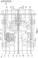
- FIG. 1 A is a schematic top view of a raindrop sensor device according to an embodiment of the disclosure.
- FIG. 1 B is a schematic cross-sectional view taken along a line A-A′ of FIG. 1 A .
- FIG. 2 is a schematic top view of a raindrop sensor device according to an embodiment of the disclosure.
- FIG. 3 A is a schematic view of a circuit of a raindrop sensor device according to an embodiment of the disclosure.
- FIG. 3 B is a timing view of a driving method of a raindrop sensor device according to an embodiment of the disclosure.
- FIG. 4 is a schematic top view of a raindrop sensor device according to an embodiment of the disclosure.
- FIG. 5 is a schematic top view of a raindrop sensor device according to an embodiment of the disclosure.
- FIG. 6 A is a schematic top view of a raindrop sensor device according to an embodiment of the disclosure.
- FIG. 6 B is a schematic cross-sectional view taken along a line B-B′ of FIG. 6 A .
- FIG. 6 C is a schematic cross-sectional view taken along a line C-C′ of FIG. 6 A .
- FIG. 7 is a schematic top view of a raindrop sensor device according to an embodiment of the disclosure.
- FIG. 8 A is a schematic view of a circuit of a raindrop sensor device according to an embodiment of the disclosure.
- FIG. 8 B is a timing view of a driving method of a raindrop sensor device according to an embodiment of the disclosure.
- FIG. 1 A is a schematic top view of a raindrop sensor device according to an embodiment of the disclosure.
- FIG. 1 B is a schematic cross-sectional view taken along a line A-A′ of FIG. 1 A .
- a raindrop sensor device 10 includes a substrate 100 , a raindrop sensor element 200 , a first light emitting diode L 1 , and a first subpixel control circuit PC 1 .
- the raindrop sensor device 10 further includes a second light emitting diode L 2 , a third light emitting diode L 3 , a second subpixel control circuit PC 2 , and a third subpixel control circuit PC 3 .
- the first subpixel control circuit PC 1 , the second subpixel control circuit PC 2 , and the third subpixel control circuit PC 3 respectively include a first active element T 1 , a second active element T 2 , and a third active element T 3 , but the disclosure is not limited thereto.
- each of the first subpixel control circuit PC 1 , the second subpixel control circuit PC 2 , and the third subpixel control circuit PC 3 may also include other active elements and/or passive elements.
- the disclosure does not limit each of the first subpixel control circuit PC 1 , the second subpixel control circuit PC 2 , and the third subpixel control circuit PC 3 to include only one active element.
- the material of the substrate 100 may be glass, quartz, organic polymer, or other applicable materials.
- the substrate 100 is suitable for a windshield of transportation means.
- the raindrop sensor element 200 is located on the substrate 100 and includes a first electrode 201 and a second electrode 202 separated from each other.
- the raindrop sensor device 10 further includes a third electrode 203 , a fourth electrode 204 , a fifth electrode 205 , and a sixth electrode 206 .
- the third electrode 203 and the fourth electrode 204 are separated from each other, and the fifth electrode 205 and the sixth electrode 206 are separated from each other.
- the first electrode 201 , the second electrode 202 , the third electrode 203 , the fourth electrode 204 , the fifth electrode 205 , and the sixth electrode 206 belong to the same conductive layer, and the material is a transparent conductive material, such as indium tin oxide, indium zinc oxide, aluminum tin oxide, aluminum zinc oxide, indium gallium zinc oxide, or a stacked layer of at least two of the above.
- each of the first electrode 201 , the second electrode 202 , the third electrode 203 , the fourth electrode 204 , the fifth electrode 205 , and the sixth electrode 206 includes a pad P and a wire C. The width of the pad P is greater than the width of the wire C.
- a raindrop R affects an electric field (or capacitance) between the first electrode 201 and the second electrode 202 , an electric field (or capacitance) between the third electrode 203 and the fourth electrode 204 , and/or an electric field (or capacitance) between the fifth electrode 205 and the sixth electrode 206 .
- the magnitude of the rain intensity may be known by changes in the electric field.
- a first insulating layer 110 (not shown in FIG. 1 A ) is located on the substrate 100 and the first electrode 201 , the second electrode 202 , the third electrode 203 , the fourth electrode 204 , the fifth electrode 205 , and the sixth electrode 206 of the raindrop sensor element 200 .
- the first active element T 1 , the second active element T 2 , and the third active element T 3 are located on the first insulating layer 110 .
- Each of the first active element T 1 , the second active element T 2 , and the third active element T 3 includes a channel layer CH, a gate G, a source S, and a drain D.
- the channel layer CH is located on the first insulating layer 110 .
- a gate insulating layer 120 (not shown in FIG. 1 A ) is located on the channel layer CH.
- the gate G is located on the gate insulating layer 120 (not shown in FIG. 1 A ) and overlaps with the channel layer CH.
- a second insulating layer 130 is located on the gate insulating layer 120 and the gate G.
- the drain D and the source S are located on the second insulating layer 130 and are electrically connected to the channel layer CH through opening O 1 and O 2 (not shown in FIG. 1 A ).
- the openings O 1 and O 2 for example, penetrate the second insulating layer 130 (not shown in FIG. 1 A ) and the gate insulating layer 120 .
- the first active element T 1 , the second active element T 2 , and the third active element T 3 are top gate thin film transistors, but the disclosure is not limited thereto. According to other embodiments, the first active element T 1 , the second active element T 2 , and the third active element T 3 are bottom gate thin film transistors, double gate thin film transistors, or other types of thin film transistors.
- the gates G of the first active element T 1 , the second active element T 2 , and the third active element T 3 are respectively electrically connected to a first scanning line SL 1 , a second scanning line SL 2 , and a third scanning line SL 3 , and the sources S of the first active element T 1 , the second active element T 2 , and the third active element T 3 are electrically connected to a data line DL at the same time, but the disclosure is not limited thereto.
- the gates G of the first active element T 1 , the second active element T 2 , and the third active element T 3 are electrically connected to a scanning line at the same time, and the sources S of the first active element T 1 , the second active element T 2 , and the third active element T 3 are respectively electrically connected to different data lines.
- the first light emitting diode L 1 , the second light emitting diode L 2 , and the third light emitting diode L 3 are located on the substrate 100 .
- the first light emitting diode L 1 , the second light emitting diode L 2 , and the third light emitting diode L 3 are located on the second insulating layer 130 .
- the drains D of the first active element T 1 , the second active element T 2 , and the third active element T 3 are respectively electrically connected to the first light emitting diode L 1 , the second light emitting diode L 2 , and the third light emitting diode L 3 .
- the first light emitting diode L 1 , the second light emitting diode L 2 , and the third light emitting diode L 3 are, for example, micro-light emitting diodes (LEDs), mini-LEDs, organic LEDs, or other suitable LEDs.
- the first light emitting diode L 1 , the second light emitting diode L 2 , and the third light emitting diode L 3 are located in the same pixel PX of the raindrop sensor device 10 , and the first light emitting diode L 1 , the second light emitting diode L 2 , and the third light emitting diode L 3 are respectively LEDs with different colors, for example, a green light emitting diode, a red light emitting diode, and a blue light emitting diode.
- the first light emitting diode L 1 , the second light emitting diode L 2 , and the third light emitting diode L 3 are suitable for displaying driving information to a driver in a vehicle or other people outside the vehicle.
- the first light emitting diode L 1 , the second light emitting diode L 2 , and the third light emitting diode L 3 are located on the same side of the substrate 100 as the raindrop sensor element 200 , for example, an inner side that is not directly exposed to the raindrop R.
- the first light emitting diode L 1 , the second light emitting diode L 2 , and the third light emitting diode L 3 emit light outwards (for example, emit light toward the substrate 100 ) to display information to drivers of other vehicles or passers-by outside the vehicle, but the disclosure is not limited thereto.
- the first light emitting diode L 1 , the second light emitting diode L 2 , and the third light emitting diode L 3 emit light inwards (for example, emit light against the substrate 100 ) to display information to the driver in the vehicle.
- each of the first light emitting diode L 1 , the second light emitting diode L 2 , and the third light emitting diode L 3 includes a semiconductor SM, a first pad PD 1 , and a second pad PD 2 .
- the semiconductor SM has, for example, a multilayer structure.
- the first pad PD 1 and the second pad PD 2 are electrically connected to the semiconductor SM.
- the first pads PD 1 of the first light emitting diode L 1 , the second light emitting diode L 2 , and the third light emitting diode L 3 are respectively electrically connected to the first electrode 201 , the third electrode 203 , and the fifth electrode 205 of the raindrop sensor element 200 .
- the second pads PD 2 of the first light emitting diode L 1 , the second light emitting diode L 2 , and the third light emitting diode L 3 are respectively electrically connected to the drains D of the first active element T 1 , the second active element T 2 , and the third active element T 3 .
- the raindrop sensor device 10 also includes multiple first transfer electrodes TE 1 (not shown in FIG. 1 A ) and multiple second transfer electrodes TE 2 (not shown in FIG. 1 A ).
- the first pads PD 1 of the first light emitting diode L 1 , the second light emitting diode L 2 , and the third light emitting diode L 3 are respectively electrically connected to the first electrode 201 , the third electrode 203 , and the fifth electrode 205 of the raindrop sensor element 200 through the corresponding first transfer electrodes TE 1 and the corresponding second transfer electrodes TE 2 .
- the first transfer electrodes TE 1 are located on the first insulating layer 110 and are respectively electrically connected to the first electrode 201 , the third electrode 203 , and the fifth electrode 205 of the raindrop sensor element 200 through multiple first through holes TH 1 (not shown in FIG. 1 A ) passing through the first insulating layer 110 .
- the gate insulating layer 120 is located on the first transfer electrode TEL
- the second transfer electrodes TE 2 are located on the second insulating layer 130 and are electrically connected to the corresponding first transfer electrodes TE 1 through multiple second through holes TH 2 (not shown in FIG. 1 A ) passing through the second insulating layer 130 .
- the second through holes TH 2 pass through the second insulating layer 130 and the gate insulating layer 120 .
- the first pad PD 1 of each of the first light emitting diode L 1 , the second light emitting diode L 2 , and the third light emitting diode L 3 is electrically connected to the corresponding second transfer electrode TE 2 .
- the first light emitting diode L 1 , the second light emitting diode L 2 , and the third light emitting diode L 3 are respectively electrically connected to the first electrode 201 , the third electrode 203 , of and the fifth electrode 205 of the raindrop sensor element 200 through the second transfer electrodes TE 2 and the first transfer electrodes TE 1 .
- the first electrode 201 , the second electrode 202 , the third electrode 203 , the fourth electrode 204 , the fifth electrode 205 , and the sixth electrode 206 of the raindrop sensor element 200 are closer to the substrate 100 than the first active element T 1 , the second active element T 2 , and the third active element T 3 , so as to prevent signals of the raindrop R from being shielded by the first subpixel control circuit PC 1 , the second subpixel control circuit PC 2 , and the third subpixel control circuit PC 3 .
- the first electrode 201 , the second electrode 202 , the third electrode 203 , the fourth electrode 204 , the fifth electrode 205 , and the sixth electrode 206 of the raindrop sensor element 200 are closer to the substrate 100 than the first light emitting diode L 1 , the second light emitting diode L 2 , and the third light emitting diode L 3 , so as to prevent the signals of the raindrop R from being shielded by the first light emitting diode L 1 , the second light emitting diode L 2 , and the third light emitting diode L 3 .
- the first electrode 201 , the first pad PD 1 of the first light emitting diode L 1 , the third electrode 203 , the first pad PD 1 of the second light emitting diode L 2 , the fifth electrode 205 , and the first pad PD 1 of the third light emitting diode L 3 are all electrically connected to a ground signal. Therefore, by electrically connecting the first pad PD 1 of the first light emitting diode L 1 to the first electrode 201 , electrically connecting the first pad PD 1 of the second light emitting diode L 2 to the third electrode 203 , and electrically connecting the first pad PD 1 of the third light emitting diode L 3 to the fifth electrode 205 , circuit layout space is saved.
- the first electrode 201 partially overlaps with the first light emitting diode L 1
- the third electrode 203 partially overlaps with the second light emitting diode L 2
- the fifth electrode 205 partially overlaps with the third light emitting diode L 3 .
- the raindrop sensor device 10 has both a raindrop sensing function and a display function.
- FIG. 2 is a schematic top view of a raindrop sensor device according to an embodiment of the disclosure. It must be noted here that the embodiment of FIG. 2 continues to use the reference numerals and some content of the embodiment of FIG. 1 A and FIG. 1 B , wherein the same or similar reference numerals are adopted to represent the same or similar elements, and the description of the same technical content is omitted. For the description of the omitted parts, reference may be made to the foregoing embodiment, which will not be repeated here.
- the difference between a raindrop sensor device 10 a of FIG. 2 and the raindrop sensor device 10 of FIG. 1 A is that: in the raindrop sensor device 10 a of FIG. 2 , the same pixel PX has the first light emitting diode L 1 , the second light emitting diode L 2 , the third light emitting diode L 3 , and a fourth light emitting diode L 4 .
- the fourth light emitting diode L 4 is, for example, a white light emitting diode, a yellow light emitting diode, or a light emitting diode with other colors.
- the raindrop sensor device 10 a further includes a fourth subpixel control circuit PC 4 and the fourth light emitting diode L 4 .
- the fourth subpixel control circuit PC 4 includes a fourth active element T 4 , and the drain D of the fourth active element T 4 is electrically connected to the second pad PD 2 of the fourth light emitting diode L 4 .
- a raindrop sensor element 200 a further includes a seventh electrode 207 and an eighth electrode 208 .
- the seventh electrode 207 and the eighth electrode 208 are separated from each other.
- the first pad PD 1 of the fourth light emitting diode L 4 is electrically connected to the seventh electrode 207 .
- the gates G of the first active element T 1 , the second active element T 2 , the third active element T 3 , and the fourth active element T 4 are respectively electrically connected to the first scanning line SL 1 , the second scanning line SL 2 , the third scanning line SL 3 , and a fourth scanning line SL 4 .
- the sources S of the first active element T 1 , the second active element T 2 , the third active element T 3 , and the fourth active element T 4 are electrically connected to the same data line DL.
- the raindrop sensor device 10 a has both the raindrop sensing function and the display function.
- FIG. 3 A is a schematic view of a circuit of a raindrop sensor device according to an embodiment of the disclosure.
- FIG. 3 B is a timing view of a driving method of a raindrop sensor device according to an embodiment of the disclosure.
- the raindrop sensor device corresponding to FIG. 3 A and FIG. 3 B is, for example, the raindrop sensor device 10 a of FIG. 2 .
- a raindrop sensor element 200 a further includes a control circuit 210 (not shown in FIG. 2 ).
- the control circuit 210 is, for example, formed on the substrate 100 .
- a capacitor C 1 includes the first electrode 201 and the second electrode 202 .
- the first electrode 201 of the capacitor C 1 is electrically connected to the first pad PD 1 of the first light emitting diode L 1
- the second electrode 202 of the capacitor C 1 is electrically connected to the control circuit 210 when a switch Q 1 is in a closed state (ON).
- a capacitor C 2 includes the third electrode 203 and the fourth electrode 204 .
- the third electrode 203 of the capacitor C 2 is electrically connected to the first pad PD 1 of the second light emitting diode L 2
- the fourth electrode 204 of the capacitor C 2 is electrically connected to the control circuit 210 when a switch Q 2 is in the closed state (ON).
- a capacitor C 3 includes the fifth electrode 205 and the sixth electrode 206 .
- the fifth electrode 205 of the capacitor C 3 is electrically connected to the first pad PD 1 of the third light emitting diode L 3
- the sixth electrode 206 of the capacitor C 3 is electrically connected to the control circuit 210 when a switch Q 3 is in the closed state (ON).
- a capacitor C 4 includes the seventh electrode 207 and the eighth electrode 208 .
- the seventh electrode 207 of the capacitor C 4 is electrically connected to the first pad PD 1 of the fourth light emitting diode L 4
- the eighth electrode 208 of the capacitor C 4 is electrically connected to the control circuit 210 when a switch Q 4 is in the closed state (ON).
- the control circuit 210 includes transistors X 1 to X 7 .
- the transistors X 1 , X 2 , and X 7 are p-type metal-oxide-semiconductor field-effect transistors.
- the transistors X 5 and X 6 are n-type metal-oxide-semiconductor field-effect transistors.
- a raindrop sensing mode of the raindrop sensor device 10 a is executed.
- the raindrop sensing mode includes a write phase and an erase phase.
- a pulse signal CL 1 is applied to the transistor X 7 of the raindrop sensor device 10 a to charge one or more of the capacitors C 1 to C 4 .
- the transistors X 1 and X 2 are in the closed state (ON)
- the transistors X 4 , X 5 , and X 6 are in an open state (OFF)
- the transistors X 3 and X 4 may be selectively in the open state or the closed state.
- a signal Vcc is transmitted to one or more of the capacitors C 1 to C 4 .
- the switches Q 1 to Q 4 between the capacitors C 1 to C 4 and the control circuit 210 may be used to determine which one (or more) of the capacitors C 1 to C 4 the signal Vcc is to be transmitted to.
- the signal Vcc is, for example, a constant voltage signal.
- an output signal Vout may be read out by a chip or other electronic elements.
- the output signal Vout of FIG. 3 A corresponds to output signals Vo 1 to Vo 4 of FIG. 3 B
- the output signals Vo 1 to Vo 4 respectively correspond to the capacitors C 1 to C 4 .
- a pulse signal CL 2 is applied to the transistors X 5 and X 6 of the raindrop sensor device 10 a to discharge the capacitors C 1 to C 4 .
- the two electrodes of each of the capacitors C 1 to C 4 are both electrically connected to a ground voltage Vss.
- the transistor X 7 is in the open state (OFF), that is, the pulse signal CL 1 is not applied to the transistor X 7 .
- the capacitor Cint is also discharged.
- the output signal Vout may be read out by a chip or other electronic elements.
- a display mode of the raindrop sensor device 10 a is executed.
- the display mode includes applying activation signals to the first active element T 1 , the second active element T 2 , the third active element T 3 , and the fourth active element T 4 .
- the first scanning line SL 1 , the second scanning line SL 2 , the third scanning line SL 3 , and the fourth scanning line SL 4 are used to sequentially apply the activation signals to the first active element T 1 , the second active element T 2 , the third active element T 3 , and the fourth active element T 4 .
- the display mode and the raindrop sensing mode of the raindrop sensor device 10 a may be executed at the same time or at different times.
- FIG. 4 is a schematic top view of a raindrop sensor device according to an embodiment of the disclosure. It must be noted here that the embodiment of FIG. 4 continues to use the reference numerals and some content of the embodiment of FIG. 1 A and FIG. 1 B , wherein the same or similar reference numerals are adopted to represent the same or similar elements, and the description of the same technical content is omitted. For the description of the omitted parts, reference may be made to the foregoing embodiment, which will not be repeated here.
- the difference between a raindrop sensor device 10 b of FIG. 4 and the raindrop sensor device 10 of FIG. 1 A is that: in the raindrop sensor device 10 b of FIG. 4 , the first light emitting diode L 1 , the second light emitting diode L 2 , and the third light emitting diode L 3 are all electrically connected to the first electrode 201 of the raindrop sensor element 200 .
- the first electrode 201 and the second electrode 202 include the pads P and the wire C electrically connected to the pads P.
- the width of the pad P is greater than the width of the wire C.
- the pad P of the first electrode 201 partially overlaps with the first light emitting diode L 1 , the second light emitting diode L 2 , and the third light emitting diode L 3 .
- the raindrop sensor device 10 b has both the raindrop sensing function and the display function.
- FIG. 5 is a schematic top view of a raindrop sensor device according to an embodiment of the disclosure. It must be noted here that the embodiment of FIG. 5 continues to use the reference numerals and some content of the embodiment of FIG. 4 , wherein the same or similar reference numerals are adopted to represent the same or similar elements, and the description of the same technical content is omitted. For the description of the omitted parts, reference may be made to the foregoing embodiment, which will not be repeated here.
- the difference between a raindrop sensor device 10 c of FIG. 5 and the raindrop sensor device 10 b of FIG. 4 is that: in the embodiment, the size of the first electrode 201 of the raindrop sensor device 10 c is greater than the size of the first light emitting diode L 1 , the size of the second light emitting diode L 2 , and the size of the third light emitting diode L 3 .
- the pad P of the first electrode 201 partially overlaps with the first light emitting diode L 1 , the second light emitting diode L 2 , and the third light emitting diode L 3 , and the size of the pad P is greater than the size of the first light emitting diode L 1 , the size of the second light emitting diode L 2 , and the size of the third light emitting diode L 3 .
- the raindrop sensor device 10 c has both the raindrop sensing function and the display function.
- FIG. 6 A is a schematic top view of a raindrop sensor device according to an embodiment of the disclosure.
- FIG. 6 B is a schematic cross-sectional view taken along a line B-B′ of FIG. 6 A .
- FIG. 6 C is a schematic cross-sectional view taken along a line C-C′ of FIG. 6 A. It must be noted here that the embodiment of FIG. 6 A to FIG. 6 C continues to use the reference numerals and some content of the embodiment of FIG. 1 A and FIG. 1 B , wherein the same or similar reference numerals are adopted to represent the same or similar elements, and the description of the same technical content is omitted. For the description of the omitted parts, reference may be made to the foregoing embodiment, which will not be repeated here.
- the difference between a raindrop sensor device 10 d of FIG. 6 A to FIG. 6 C and the raindrop sensor device 10 of FIG. 1 A is that: the raindrop sensor device 10 d of FIG. 6 A to FIG. 6 C further includes a first switch element SW 1 , a second switch element SW 2 , and a third switch element SW 3 .
- the first switch element SW 1 , the second switch element SW 2 , and the third switch element SW 3 are located on the substrate 100 .
- Each of the first switch element SW 1 , the second switch element SW 2 , and the third switch element SW 3 includes a channel layer CHa, a gate Ga, a source Sa, and a drain Da.
- the channel layer CHa is located on the first insulating layer 110 (not shown in FIG. 6 A ).
- the gate insulating layer 120 (not shown in FIG. 6 A ) is located on the channel layer CHa.
- the gate Ga is located on the gate insulating layer 120 and overlaps with the channel layer CHa.
- the second insulating layer 130 is located on the gate insulating layer 120 and the gate Ga.
- the drain Da and the source Sa are located on the second insulating layer 130 (not shown in FIG. 6 A ) and are electrically connected to the channel layer CHa through openings O 3 and O 4 (not shown in FIG. 6 A ).
- the openings O 3 and O 4 for example, penetrate the second insulating layer 130 and the gate insulating layer 120 .
- the first switch element SW 1 , the second switch element SW 2 , and the third switch element SW 3 are top gate thin film transistors, but the disclosure is not limited thereto. According to other embodiments, the first switch element SW 1 , the second switch element SW 2 , and the third switch element SW 3 are bottom gate thin film transistors, double gate thin film transistors, or other types of thin film transistors.
- the gates Ga of the first switch element SW 1 , the second switch element SW 2 , and the third switch element SW 3 are respectively electrically connected to a first control line Y 1 , a second control line Y 2 , and a third control line Y 3 .
- the source Sa of the first switch element SW 1 is electrically connected to the drain D of the first active element T 1 and the second pad PD 2 of the first light emitting diode L 1
- the source Sa of the second switch element SW 2 is electrically connected to the drain D of the second active element T 2 and the second pad PD 2 of the second light emitting diode L 2
- the source Sa of the third switch element SW 3 is electrically connected to the drain D of the third active element T 3 and the second pad PD 2 of the third light emitting diode L 3 .
- the drain Da of the first switch element SW 1 is electrically connected to the second electrode 202 of the raindrop sensor element 200
- the drain Da of the second switch element SW 2 is electrically connected to the fourth electrode 204 of the raindrop sensor element 200
- the drain Da of the third switch element SW 3 is electrically connected to the sixth electrode 206 of the raindrop sensor element 200
- the drain Da of the first switch element SW 1 , the drain Da of the second switch element SW 2 , and the drain Da of the third switch element SW 3 are also electrically connected to the control circuit of the raindrop sensor element 200 (not shown in FIG. 6 A ).
- multiple third transfer electrodes TE 3 (not shown in FIG.
- the gate insulating layer 120 is located on the third transfer electrode TE 3 .
- the drain Da of the first switch element SW 1 , the drain Da of the second switch element SW 2 , and the drain Da of the third switch element SW 3 are located on the second insulating layer 130 and are respectively electrically connected to through the third transfer electrodes TE 3 through multiple fourth through holes TH 4 passing through the second insulating layer 130 .
- the first switch element SW 1 , the second switch element SW 2 , and the third switch element SW 3 may prevent the control circuit of the raindrop sensor element 200 in the display mode from interfering with the first light emitting diode L 1 , the second light emitting diode L 2 , and the third light emitting diode L 3 .
- FIG. 7 is a schematic top view of a raindrop sensor device according to an embodiment of the disclosure. It must be noted here that the embodiment of FIG. 7 continues to use the reference numerals and some content of the embodiment of FIG. 6 A to FIG. 6 C , wherein the same or similar reference numerals are adopted to represent the same or similar elements, and the description of the same technical content is omitted. For the description of the omitted parts, reference may be made to the foregoing embodiment, which will not be repeated here.
- the difference between a raindrop sensor device 10 e of FIG. 7 and the raindrop sensor device 10 d of FIG. 6 A to FIG. 6 C is that: in the raindrop sensor device 10 e of FIG. 7 , the same pixel PX has the first light emitting diode L 1 , the second light emitting diode L 2 , the third light emitting diode L 3 , and the fourth light emitting diode L 4 .
- the fourth light emitting diode L 4 is, for example, a white light emitting diode, a yellow light emitting diode, or a light emitting diode with other colors.
- the raindrop sensor device 10 e further includes the fourth subpixel control circuit PC 4 , the fourth light emitting diode L 4 , and a fourth switch element SW 4 .
- the fourth subpixel control circuit PC 4 includes the fourth active element T 4 , and the drain of the fourth active element T 4 is electrically connected to the source Sa of the fourth switch element SW 4 and the second pad PD 2 of the fourth light emitting diode L 4 .
- the raindrop sensor element 200 a further includes the seventh electrode 207 and the eighth electrode 208 .
- the seventh electrode 207 and the eighth electrode 208 are separated from each other.
- the first pad PD 1 of the fourth light emitting diode L 4 is electrically connected to the seventh electrode 207 .
- the drain of the fourth switch element SW 4 is electrically connected to the eighth electrode 208 .
- the gates G of the first active element T 1 , the second active element T 2 , the third active element T 3 , and the fourth active element T 4 are respectively electrically connected to the first scanning line SL 1 , the second scanning line SL 2 , the third scanning line SL 3 , and the fourth scanning line SL 4 .
- the gates Ga of the first switch element SW 1 , the second switch element SW 2 , the third switch element SW 3 , and the fourth switch element SW 4 are respectively electrically connected to the first control line Y 1 , the second control line Y 2 , the third control line Y 3 , and the fourth control line Y 4 .
- the source S of each of the first active element T 1 , the second active element T 2 , the third active element T 3 , and the fourth active element T 4 is electrically connected to the same data line DL.
- the raindrop sensor device 10 e has both the raindrop sensing function and the display function.
- FIG. 8 A is a schematic view of a circuit of a raindrop sensor device according to an embodiment of the disclosure.
- FIG. 8 B is a timing view of a driving method of a raindrop sensor device according to an embodiment of the disclosure.
- the raindrop sensor device corresponding to FIG. 8 A and FIG. 8 B is, for example, the raindrop sensor device 10 e of FIG. 7 .
- the raindrop sensor element 200 a further includes the control circuit 210 (not shown in FIG. 2 ).
- the control circuit 210 for the related description of the control circuit 210 , reference may be made to the relevant paragraphs of FIG. 3 A and FIG. 3 A , which will not be repeated here.
- signals of the first control line Y 1 , the second control line Y 2 , the third control line Y 3 , and the fourth control line Y 4 are pulled down, so that the first switch element SW 1 , the second switch element SW 2 , the third switch element SW 3 , and the fourth switch element SW 4 are in the open state (OFF) to prevent the control circuit 210 from affecting the first light emitting diode L 1 , the second light emitting diode L 2 , the third light emitting diode L 3 , and the fourth light emitting diode L 4 .
- the signals of the first control line Y 1 , the second control line Y 2 , the third control line Y 3 , and the fourth control line Y 4 are pulled up, so that the first switch element SW 1 , the second switch element SW 2 , the third switch element SW 3 , and the fourth switch element SW 4 are in the closed state (ON).
- the switches Q 1 to Q 4 are disconnected, so as to prevent the control circuit 210 from affecting the first light emitting diode L 1 , the second light emitting diode L 2 , the third light emitting diode L 3 , and the fourth light emitting diode L 4 .
- the display mode and the raindrop sensing mode of the raindrop sensor device 10 e are not executed at the same time. In other words, the display mode and the raindrop sensing mode of the raindrop sensor device 10 e may be alternately executed.
Abstract
Description
Claims (15)
Priority Applications (1)
| Application Number | Priority Date | Filing Date | Title |
|---|---|---|---|
| US17/386,500 US11891022B2 (en) | 2020-10-12 | 2021-07-27 | Raindrop sensor device and driving method thereof |
Applications Claiming Priority (4)
| Application Number | Priority Date | Filing Date | Title |
|---|---|---|---|
| US202063090330P | 2020-10-12 | 2020-10-12 | |
| TW110112663A TWI765646B (en) | 2020-10-12 | 2021-04-08 | Raindrop sensor device and driving method thereof |
| TW110112663 | 2021-04-08 | ||
| US17/386,500 US11891022B2 (en) | 2020-10-12 | 2021-07-27 | Raindrop sensor device and driving method thereof |
Publications (2)
| Publication Number | Publication Date |
|---|---|
| US20220111821A1 US20220111821A1 (en) | 2022-04-14 |
| US11891022B2 true US11891022B2 (en) | 2024-02-06 |
Family
ID=78962040
Family Applications (1)
| Application Number | Title | Priority Date | Filing Date |
|---|---|---|---|
| US17/386,500 Active 2042-08-04 US11891022B2 (en) | 2020-10-12 | 2021-07-27 | Raindrop sensor device and driving method thereof |
Country Status (2)
| Country | Link |
|---|---|
| US (1) | US11891022B2 (en) |
| CN (1) | CN113830028B (en) |
Citations (10)
| Publication number | Priority date | Publication date | Assignee | Title |
|---|---|---|---|---|
| US4973844A (en) * | 1989-07-10 | 1990-11-27 | Donnelly Corporation | Vehicular moisture sensor and mounting apparatus therefor |
| US7019322B2 (en) * | 2001-07-06 | 2006-03-28 | Robert Bosch Gmbh | Optical sensor for detecting moisture on a surface |
| CN202563207U (en) | 2012-04-20 | 2012-11-28 | 北京京东方光电科技有限公司 | Touch display module and display device |
| US20150042599A1 (en) | 2013-08-07 | 2015-02-12 | Synaptics Incorporated | Capacitive sensing using a matrix electrode pattern |
| CN104460411A (en) | 2014-10-24 | 2015-03-25 | 苏州佑瑞检测技术有限公司 | Car inside environment monitoring system based on projecting device and rain and dew detection device |
| CN204789597U (en) | 2015-02-17 | 2015-11-18 | 星宇资源公司 | Liquid phase detects chip |
| US9234983B2 (en) * | 2012-03-28 | 2016-01-12 | Denso Corporation | Rain sensor |
| US9371032B2 (en) | 2006-01-10 | 2016-06-21 | Guardian Industries Corp. | Moisture sensor and/or defogger with Bayesian improvements, and related methods |
| CN110459567A (en) | 2019-01-17 | 2019-11-15 | 友达光电股份有限公司 | Light emitting device |
| CN211617631U (en) | 2020-01-07 | 2020-10-02 | 深圳南方德尔汽车电子有限公司 | Integrated multifunctional vehicle sensor device |
Family Cites Families (14)
| Publication number | Priority date | Publication date | Assignee | Title |
|---|---|---|---|---|
| JPS62179648A (en) * | 1986-01-31 | 1987-08-06 | Toyota Motor Corp | Rain drop detector |
| JP3135961B2 (en) * | 1991-12-27 | 2001-02-19 | 自動車電機工業株式会社 | Wiper drive |
| JP3772889B2 (en) * | 2003-05-19 | 2006-05-10 | セイコーエプソン株式会社 | Electro-optical device and driving device thereof |
| JP4514674B2 (en) * | 2005-08-16 | 2010-07-28 | シャープ株式会社 | Display device, display panel substrate, and display panel substrate manufacturing method |
| WO2007029248A2 (en) * | 2005-09-06 | 2007-03-15 | Tamar Sensors Ltd. | Sealed capacitive rain sensor |
| US8354674B2 (en) * | 2007-06-29 | 2013-01-15 | Semiconductor Energy Laboratory Co., Ltd. | Semiconductor device wherein a property of a first semiconductor layer is different from a property of a second semiconductor layer |
| WO2010001590A1 (en) * | 2008-07-04 | 2010-01-07 | パナソニック株式会社 | Display device and method for controlling the same |
| CN101392584B (en) * | 2008-10-15 | 2010-08-25 | 王金友 | Electric awning and rain detecting sensor |
| US20100201275A1 (en) * | 2009-02-06 | 2010-08-12 | Cok Ronald S | Light sensing in display device |
| KR102503129B1 (en) * | 2016-07-22 | 2023-02-23 | 엘지이노텍 주식회사 | Rain sensor and wiper driving device including same |
| CN107340371A (en) * | 2017-08-01 | 2017-11-10 | 深圳市盛路物联通讯技术有限公司 | A kind of water quality detection method and system |
| CN108957516B (en) * | 2018-06-26 | 2021-09-17 | 南京航空航天大学 | Radioactivity measuring device with self-correcting function and measuring method thereof |
| CN108919385A (en) * | 2018-09-05 | 2018-11-30 | 湖北第二师范学院 | A kind of capacitive rainfall sensor |
| TWI679569B (en) * | 2018-11-26 | 2019-12-11 | 友達光電股份有限公司 | Display apparatus |
-
2021
- 2021-07-27 US US17/386,500 patent/US11891022B2/en active Active
- 2021-09-02 CN CN202111026243.9A patent/CN113830028B/en active Active
Patent Citations (14)
| Publication number | Priority date | Publication date | Assignee | Title |
|---|---|---|---|---|
| US4973844A (en) * | 1989-07-10 | 1990-11-27 | Donnelly Corporation | Vehicular moisture sensor and mounting apparatus therefor |
| US7019322B2 (en) * | 2001-07-06 | 2006-03-28 | Robert Bosch Gmbh | Optical sensor for detecting moisture on a surface |
| US9371032B2 (en) | 2006-01-10 | 2016-06-21 | Guardian Industries Corp. | Moisture sensor and/or defogger with Bayesian improvements, and related methods |
| US9234983B2 (en) * | 2012-03-28 | 2016-01-12 | Denso Corporation | Rain sensor |
| CN202563207U (en) | 2012-04-20 | 2012-11-28 | 北京京东方光电科技有限公司 | Touch display module and display device |
| US20150042599A1 (en) | 2013-08-07 | 2015-02-12 | Synaptics Incorporated | Capacitive sensing using a matrix electrode pattern |
| CN105556446A (en) | 2013-08-07 | 2016-05-04 | 辛纳普蒂克斯公司 | Electronic device, method for controlling electronic device, and storage medium |
| US20150042600A1 (en) | 2013-08-07 | 2015-02-12 | Synaptics Incorporated | Capacitive sensing using a matrix electrode pattern |
| US9542023B2 (en) | 2013-08-07 | 2017-01-10 | Synaptics Incorporated | Capacitive sensing using matrix electrodes driven by routing traces disposed in a source line layer |
| US9552089B2 (en) | 2013-08-07 | 2017-01-24 | Synaptics Incorporated | Capacitive sensing using a matrix electrode pattern |
| CN104460411A (en) | 2014-10-24 | 2015-03-25 | 苏州佑瑞检测技术有限公司 | Car inside environment monitoring system based on projecting device and rain and dew detection device |
| CN204789597U (en) | 2015-02-17 | 2015-11-18 | 星宇资源公司 | Liquid phase detects chip |
| CN110459567A (en) | 2019-01-17 | 2019-11-15 | 友达光电股份有限公司 | Light emitting device |
| CN211617631U (en) | 2020-01-07 | 2020-10-02 | 深圳南方德尔汽车电子有限公司 | Integrated multifunctional vehicle sensor device |
Also Published As
| Publication number | Publication date |
|---|---|
| US20220111821A1 (en) | 2022-04-14 |
| CN113830028B (en) | 2023-11-10 |
| CN113830028A (en) | 2021-12-24 |
Similar Documents
| Publication | Publication Date | Title |
|---|---|---|
| AU2019261689B2 (en) | Display panel and crack detecting method thereof, display apparatus | |
| US10042193B2 (en) | Liquid crystal display device and method for manufacturing the same | |
| US11495168B2 (en) | Display device, backlight module and electronic device | |
| US20130146866A1 (en) | Circuit board, display device, and method for producing circuit board | |
| US20190064256A1 (en) | Test circuit, array substrate and manufacturing method thereof, and display device | |
| CN101266349B (en) | Display device | |
| US20090072226A1 (en) | Display device having organic thin film transistor | |
| KR20230095446A (en) | Display apparatus | |
| US10403209B2 (en) | Array substrate, electrical aging method, display device and manufacturing method thereof | |
| US9129578B2 (en) | Shift register circuit and display device using the same | |
| US20200348772A1 (en) | Touch display device | |
| US11891022B2 (en) | Raindrop sensor device and driving method thereof | |
| CN110326113B (en) | Drive circuit, TFT substrate and display device | |
| CN100585476C (en) | Liquid crystal displaying device | |
| TWI765646B (en) | Raindrop sensor device and driving method thereof | |
| KR20040075734A (en) | Electro-optical device and method of manufacturing the same and electronic instrument | |
| US9673334B2 (en) | Low temperature poly silicon thin film transistors (LTPS TFTs) and TFT substrates | |
| US20240013682A1 (en) | Electronic shelf label | |
| US20230207318A1 (en) | Display panel, tiled display device including the same, and method of manufacturing display panel | |
| CN111785203B (en) | Driving method and driving device of light emitting circuit | |
| US20210263356A1 (en) | Thin-film transistor array and method of producing the same | |
| KR20230095657A (en) | Display appratus and method of thereof | |
| CN114497076A (en) | Display device | |
| US20090237609A1 (en) | Display Device | |
| CN113534551A (en) | Display substrate and display panel |
Legal Events
| Date | Code | Title | Description |
|---|---|---|---|
| FEPP | Fee payment procedure |
Free format text: ENTITY STATUS SET TO UNDISCOUNTED (ORIGINAL EVENT CODE: BIG.); ENTITY STATUS OF PATENT OWNER: LARGE ENTITY |
|
| AS | Assignment |
Owner name: AU OPTRONICS CORPORATION, TAIWAN Free format text: ASSIGNMENT OF ASSIGNORS INTEREST;ASSIGNORS:LEE, CHIA-CHI;HUANG, PAO-YU;REEL/FRAME:057059/0714 Effective date: 20210723 |
|
| STPP | Information on status: patent application and granting procedure in general |
Free format text: DOCKETED NEW CASE - READY FOR EXAMINATION |
|
| STPP | Information on status: patent application and granting procedure in general |
Free format text: NON FINAL ACTION MAILED |
|
| STPP | Information on status: patent application and granting procedure in general |
Free format text: RESPONSE TO NON-FINAL OFFICE ACTION ENTERED AND FORWARDED TO EXAMINER |
|
| STPP | Information on status: patent application and granting procedure in general |
Free format text: NOTICE OF ALLOWANCE MAILED -- APPLICATION RECEIVED IN OFFICE OF PUBLICATIONS |
|
| STPP | Information on status: patent application and granting procedure in general |
Free format text: PUBLICATIONS -- ISSUE FEE PAYMENT RECEIVED |
|
| STPP | Information on status: patent application and granting procedure in general |
Free format text: PUBLICATIONS -- ISSUE FEE PAYMENT VERIFIED |
|
| STCF | Information on status: patent grant |
Free format text: PATENTED CASE |