US11830438B2 - Display device - Google Patents
Display device Download PDFInfo
- Publication number
- US11830438B2 US11830438B2 US18/088,551 US202218088551A US11830438B2 US 11830438 B2 US11830438 B2 US 11830438B2 US 202218088551 A US202218088551 A US 202218088551A US 11830438 B2 US11830438 B2 US 11830438B2
- Authority
- US
- United States
- Prior art keywords
- scan
- transistor
- pixels
- period
- frequency
- Prior art date
- Legal status (The legal status is an assumption and is not a legal conclusion. Google has not performed a legal analysis and makes no representation as to the accuracy of the status listed.)
- Active
Links
- 239000003990 capacitor Substances 0.000 claims description 24
- 239000004065 semiconductor Substances 0.000 claims description 24
- 238000010586 diagram Methods 0.000 description 45
- 238000000034 method Methods 0.000 description 26
- 230000004044 response Effects 0.000 description 20
- 102100022887 GTP-binding nuclear protein Ran Human genes 0.000 description 19
- 101000774835 Heteractis crispa PI-stichotoxin-Hcr2o Proteins 0.000 description 19
- 101000620756 Homo sapiens GTP-binding nuclear protein Ran Proteins 0.000 description 19
- 101100393821 Saccharomyces cerevisiae (strain ATCC 204508 / S288c) GSP2 gene Proteins 0.000 description 17
- 239000008186 active pharmaceutical agent Substances 0.000 description 17
- 230000003252 repetitive effect Effects 0.000 description 12
- 229910021420 polycrystalline silicon Inorganic materials 0.000 description 7
- 230000003071 parasitic effect Effects 0.000 description 6
- 230000001360 synchronised effect Effects 0.000 description 5
- 101100448444 Caenorhabditis elegans gsp-3 gene Proteins 0.000 description 4
- 238000004519 manufacturing process Methods 0.000 description 3
- 230000008569 process Effects 0.000 description 3
- 230000009467 reduction Effects 0.000 description 2
- 230000008878 coupling Effects 0.000 description 1
- 238000010168 coupling process Methods 0.000 description 1
- 238000005859 coupling reaction Methods 0.000 description 1
- 229910010272 inorganic material Inorganic materials 0.000 description 1
- 239000011147 inorganic material Substances 0.000 description 1
- 230000007704 transition Effects 0.000 description 1
Images


Classifications
-
- G—PHYSICS
- G09—EDUCATION; CRYPTOGRAPHY; DISPLAY; ADVERTISING; SEALS
- G09G—ARRANGEMENTS OR CIRCUITS FOR CONTROL OF INDICATING DEVICES USING STATIC MEANS TO PRESENT VARIABLE INFORMATION
- G09G3/00—Control arrangements or circuits, of interest only in connection with visual indicators other than cathode-ray tubes
- G09G3/20—Control arrangements or circuits, of interest only in connection with visual indicators other than cathode-ray tubes for presentation of an assembly of a number of characters, e.g. a page, by composing the assembly by combination of individual elements arranged in a matrix no fixed position being assigned to or needed to be assigned to the individual characters or partial characters
- G09G3/22—Control arrangements or circuits, of interest only in connection with visual indicators other than cathode-ray tubes for presentation of an assembly of a number of characters, e.g. a page, by composing the assembly by combination of individual elements arranged in a matrix no fixed position being assigned to or needed to be assigned to the individual characters or partial characters using controlled light sources
- G09G3/30—Control arrangements or circuits, of interest only in connection with visual indicators other than cathode-ray tubes for presentation of an assembly of a number of characters, e.g. a page, by composing the assembly by combination of individual elements arranged in a matrix no fixed position being assigned to or needed to be assigned to the individual characters or partial characters using controlled light sources using electroluminescent panels
- G09G3/32—Control arrangements or circuits, of interest only in connection with visual indicators other than cathode-ray tubes for presentation of an assembly of a number of characters, e.g. a page, by composing the assembly by combination of individual elements arranged in a matrix no fixed position being assigned to or needed to be assigned to the individual characters or partial characters using controlled light sources using electroluminescent panels semiconductive, e.g. using light-emitting diodes [LED]
- G09G3/3208—Control arrangements or circuits, of interest only in connection with visual indicators other than cathode-ray tubes for presentation of an assembly of a number of characters, e.g. a page, by composing the assembly by combination of individual elements arranged in a matrix no fixed position being assigned to or needed to be assigned to the individual characters or partial characters using controlled light sources using electroluminescent panels semiconductive, e.g. using light-emitting diodes [LED] organic, e.g. using organic light-emitting diodes [OLED]
- G09G3/3266—Details of drivers for scan electrodes
-
- G—PHYSICS
- G09—EDUCATION; CRYPTOGRAPHY; DISPLAY; ADVERTISING; SEALS
- G09G—ARRANGEMENTS OR CIRCUITS FOR CONTROL OF INDICATING DEVICES USING STATIC MEANS TO PRESENT VARIABLE INFORMATION
- G09G3/00—Control arrangements or circuits, of interest only in connection with visual indicators other than cathode-ray tubes
- G09G3/20—Control arrangements or circuits, of interest only in connection with visual indicators other than cathode-ray tubes for presentation of an assembly of a number of characters, e.g. a page, by composing the assembly by combination of individual elements arranged in a matrix no fixed position being assigned to or needed to be assigned to the individual characters or partial characters
- G09G3/22—Control arrangements or circuits, of interest only in connection with visual indicators other than cathode-ray tubes for presentation of an assembly of a number of characters, e.g. a page, by composing the assembly by combination of individual elements arranged in a matrix no fixed position being assigned to or needed to be assigned to the individual characters or partial characters using controlled light sources
- G09G3/30—Control arrangements or circuits, of interest only in connection with visual indicators other than cathode-ray tubes for presentation of an assembly of a number of characters, e.g. a page, by composing the assembly by combination of individual elements arranged in a matrix no fixed position being assigned to or needed to be assigned to the individual characters or partial characters using controlled light sources using electroluminescent panels
- G09G3/32—Control arrangements or circuits, of interest only in connection with visual indicators other than cathode-ray tubes for presentation of an assembly of a number of characters, e.g. a page, by composing the assembly by combination of individual elements arranged in a matrix no fixed position being assigned to or needed to be assigned to the individual characters or partial characters using controlled light sources using electroluminescent panels semiconductive, e.g. using light-emitting diodes [LED]
- G09G3/3208—Control arrangements or circuits, of interest only in connection with visual indicators other than cathode-ray tubes for presentation of an assembly of a number of characters, e.g. a page, by composing the assembly by combination of individual elements arranged in a matrix no fixed position being assigned to or needed to be assigned to the individual characters or partial characters using controlled light sources using electroluminescent panels semiconductive, e.g. using light-emitting diodes [LED] organic, e.g. using organic light-emitting diodes [OLED]
- G09G3/3225—Control arrangements or circuits, of interest only in connection with visual indicators other than cathode-ray tubes for presentation of an assembly of a number of characters, e.g. a page, by composing the assembly by combination of individual elements arranged in a matrix no fixed position being assigned to or needed to be assigned to the individual characters or partial characters using controlled light sources using electroluminescent panels semiconductive, e.g. using light-emitting diodes [LED] organic, e.g. using organic light-emitting diodes [OLED] using an active matrix
- G09G3/3233—Control arrangements or circuits, of interest only in connection with visual indicators other than cathode-ray tubes for presentation of an assembly of a number of characters, e.g. a page, by composing the assembly by combination of individual elements arranged in a matrix no fixed position being assigned to or needed to be assigned to the individual characters or partial characters using controlled light sources using electroluminescent panels semiconductive, e.g. using light-emitting diodes [LED] organic, e.g. using organic light-emitting diodes [OLED] using an active matrix with pixel circuitry controlling the current through the light-emitting element
-
- G—PHYSICS
- G09—EDUCATION; CRYPTOGRAPHY; DISPLAY; ADVERTISING; SEALS
- G09G—ARRANGEMENTS OR CIRCUITS FOR CONTROL OF INDICATING DEVICES USING STATIC MEANS TO PRESENT VARIABLE INFORMATION
- G09G3/00—Control arrangements or circuits, of interest only in connection with visual indicators other than cathode-ray tubes
- G09G3/20—Control arrangements or circuits, of interest only in connection with visual indicators other than cathode-ray tubes for presentation of an assembly of a number of characters, e.g. a page, by composing the assembly by combination of individual elements arranged in a matrix no fixed position being assigned to or needed to be assigned to the individual characters or partial characters
- G09G3/22—Control arrangements or circuits, of interest only in connection with visual indicators other than cathode-ray tubes for presentation of an assembly of a number of characters, e.g. a page, by composing the assembly by combination of individual elements arranged in a matrix no fixed position being assigned to or needed to be assigned to the individual characters or partial characters using controlled light sources
- G09G3/30—Control arrangements or circuits, of interest only in connection with visual indicators other than cathode-ray tubes for presentation of an assembly of a number of characters, e.g. a page, by composing the assembly by combination of individual elements arranged in a matrix no fixed position being assigned to or needed to be assigned to the individual characters or partial characters using controlled light sources using electroluminescent panels
- G09G3/32—Control arrangements or circuits, of interest only in connection with visual indicators other than cathode-ray tubes for presentation of an assembly of a number of characters, e.g. a page, by composing the assembly by combination of individual elements arranged in a matrix no fixed position being assigned to or needed to be assigned to the individual characters or partial characters using controlled light sources using electroluminescent panels semiconductive, e.g. using light-emitting diodes [LED]
- G09G3/3208—Control arrangements or circuits, of interest only in connection with visual indicators other than cathode-ray tubes for presentation of an assembly of a number of characters, e.g. a page, by composing the assembly by combination of individual elements arranged in a matrix no fixed position being assigned to or needed to be assigned to the individual characters or partial characters using controlled light sources using electroluminescent panels semiconductive, e.g. using light-emitting diodes [LED] organic, e.g. using organic light-emitting diodes [OLED]
-
- G—PHYSICS
- G09—EDUCATION; CRYPTOGRAPHY; DISPLAY; ADVERTISING; SEALS
- G09G—ARRANGEMENTS OR CIRCUITS FOR CONTROL OF INDICATING DEVICES USING STATIC MEANS TO PRESENT VARIABLE INFORMATION
- G09G3/00—Control arrangements or circuits, of interest only in connection with visual indicators other than cathode-ray tubes
- G09G3/20—Control arrangements or circuits, of interest only in connection with visual indicators other than cathode-ray tubes for presentation of an assembly of a number of characters, e.g. a page, by composing the assembly by combination of individual elements arranged in a matrix no fixed position being assigned to or needed to be assigned to the individual characters or partial characters
- G09G3/2092—Details of a display terminals using a flat panel, the details relating to the control arrangement of the display terminal and to the interfaces thereto
-
- G—PHYSICS
- G09—EDUCATION; CRYPTOGRAPHY; DISPLAY; ADVERTISING; SEALS
- G09G—ARRANGEMENTS OR CIRCUITS FOR CONTROL OF INDICATING DEVICES USING STATIC MEANS TO PRESENT VARIABLE INFORMATION
- G09G3/00—Control arrangements or circuits, of interest only in connection with visual indicators other than cathode-ray tubes
- G09G3/20—Control arrangements or circuits, of interest only in connection with visual indicators other than cathode-ray tubes for presentation of an assembly of a number of characters, e.g. a page, by composing the assembly by combination of individual elements arranged in a matrix no fixed position being assigned to or needed to be assigned to the individual characters or partial characters
- G09G3/22—Control arrangements or circuits, of interest only in connection with visual indicators other than cathode-ray tubes for presentation of an assembly of a number of characters, e.g. a page, by composing the assembly by combination of individual elements arranged in a matrix no fixed position being assigned to or needed to be assigned to the individual characters or partial characters using controlled light sources
- G09G3/30—Control arrangements or circuits, of interest only in connection with visual indicators other than cathode-ray tubes for presentation of an assembly of a number of characters, e.g. a page, by composing the assembly by combination of individual elements arranged in a matrix no fixed position being assigned to or needed to be assigned to the individual characters or partial characters using controlled light sources using electroluminescent panels
- G09G3/32—Control arrangements or circuits, of interest only in connection with visual indicators other than cathode-ray tubes for presentation of an assembly of a number of characters, e.g. a page, by composing the assembly by combination of individual elements arranged in a matrix no fixed position being assigned to or needed to be assigned to the individual characters or partial characters using controlled light sources using electroluminescent panels semiconductive, e.g. using light-emitting diodes [LED]
- G09G3/3208—Control arrangements or circuits, of interest only in connection with visual indicators other than cathode-ray tubes for presentation of an assembly of a number of characters, e.g. a page, by composing the assembly by combination of individual elements arranged in a matrix no fixed position being assigned to or needed to be assigned to the individual characters or partial characters using controlled light sources using electroluminescent panels semiconductive, e.g. using light-emitting diodes [LED] organic, e.g. using organic light-emitting diodes [OLED]
- G09G3/3275—Details of drivers for data electrodes
- G09G3/3291—Details of drivers for data electrodes in which the data driver supplies a variable data voltage for setting the current through, or the voltage across, the light-emitting elements
-
- G—PHYSICS
- G09—EDUCATION; CRYPTOGRAPHY; DISPLAY; ADVERTISING; SEALS
- G09G—ARRANGEMENTS OR CIRCUITS FOR CONTROL OF INDICATING DEVICES USING STATIC MEANS TO PRESENT VARIABLE INFORMATION
- G09G2300/00—Aspects of the constitution of display devices
- G09G2300/04—Structural and physical details of display devices
- G09G2300/0404—Matrix technologies
-
- G—PHYSICS
- G09—EDUCATION; CRYPTOGRAPHY; DISPLAY; ADVERTISING; SEALS
- G09G—ARRANGEMENTS OR CIRCUITS FOR CONTROL OF INDICATING DEVICES USING STATIC MEANS TO PRESENT VARIABLE INFORMATION
- G09G2300/00—Aspects of the constitution of display devices
- G09G2300/08—Active matrix structure, i.e. with use of active elements, inclusive of non-linear two terminal elements, in the pixels together with light emitting or modulating elements
- G09G2300/0809—Several active elements per pixel in active matrix panels
- G09G2300/0819—Several active elements per pixel in active matrix panels used for counteracting undesired variations, e.g. feedback or autozeroing
-
- G—PHYSICS
- G09—EDUCATION; CRYPTOGRAPHY; DISPLAY; ADVERTISING; SEALS
- G09G—ARRANGEMENTS OR CIRCUITS FOR CONTROL OF INDICATING DEVICES USING STATIC MEANS TO PRESENT VARIABLE INFORMATION
- G09G2300/00—Aspects of the constitution of display devices
- G09G2300/08—Active matrix structure, i.e. with use of active elements, inclusive of non-linear two terminal elements, in the pixels together with light emitting or modulating elements
- G09G2300/0809—Several active elements per pixel in active matrix panels
- G09G2300/0842—Several active elements per pixel in active matrix panels forming a memory circuit, e.g. a dynamic memory with one capacitor
- G09G2300/0852—Several active elements per pixel in active matrix panels forming a memory circuit, e.g. a dynamic memory with one capacitor being a dynamic memory with more than one capacitor
-
- G—PHYSICS
- G09—EDUCATION; CRYPTOGRAPHY; DISPLAY; ADVERTISING; SEALS
- G09G—ARRANGEMENTS OR CIRCUITS FOR CONTROL OF INDICATING DEVICES USING STATIC MEANS TO PRESENT VARIABLE INFORMATION
- G09G2300/00—Aspects of the constitution of display devices
- G09G2300/08—Active matrix structure, i.e. with use of active elements, inclusive of non-linear two terminal elements, in the pixels together with light emitting or modulating elements
- G09G2300/0809—Several active elements per pixel in active matrix panels
- G09G2300/0842—Several active elements per pixel in active matrix panels forming a memory circuit, e.g. a dynamic memory with one capacitor
- G09G2300/0861—Several active elements per pixel in active matrix panels forming a memory circuit, e.g. a dynamic memory with one capacitor with additional control of the display period without amending the charge stored in a pixel memory, e.g. by means of additional select electrodes
-
- G—PHYSICS
- G09—EDUCATION; CRYPTOGRAPHY; DISPLAY; ADVERTISING; SEALS
- G09G—ARRANGEMENTS OR CIRCUITS FOR CONTROL OF INDICATING DEVICES USING STATIC MEANS TO PRESENT VARIABLE INFORMATION
- G09G2310/00—Command of the display device
- G09G2310/06—Details of flat display driving waveforms
-
- G—PHYSICS
- G09—EDUCATION; CRYPTOGRAPHY; DISPLAY; ADVERTISING; SEALS
- G09G—ARRANGEMENTS OR CIRCUITS FOR CONTROL OF INDICATING DEVICES USING STATIC MEANS TO PRESENT VARIABLE INFORMATION
- G09G2310/00—Command of the display device
- G09G2310/08—Details of timing specific for flat panels, other than clock recovery
-
- G—PHYSICS
- G09—EDUCATION; CRYPTOGRAPHY; DISPLAY; ADVERTISING; SEALS
- G09G—ARRANGEMENTS OR CIRCUITS FOR CONTROL OF INDICATING DEVICES USING STATIC MEANS TO PRESENT VARIABLE INFORMATION
- G09G2320/00—Control of display operating conditions
- G09G2320/02—Improving the quality of display appearance
- G09G2320/0238—Improving the black level
-
- G—PHYSICS
- G09—EDUCATION; CRYPTOGRAPHY; DISPLAY; ADVERTISING; SEALS
- G09G—ARRANGEMENTS OR CIRCUITS FOR CONTROL OF INDICATING DEVICES USING STATIC MEANS TO PRESENT VARIABLE INFORMATION
- G09G2320/00—Control of display operating conditions
- G09G2320/02—Improving the quality of display appearance
- G09G2320/0247—Flicker reduction other than flicker reduction circuits used for single beam cathode-ray tubes
-
- G—PHYSICS
- G09—EDUCATION; CRYPTOGRAPHY; DISPLAY; ADVERTISING; SEALS
- G09G—ARRANGEMENTS OR CIRCUITS FOR CONTROL OF INDICATING DEVICES USING STATIC MEANS TO PRESENT VARIABLE INFORMATION
- G09G2330/00—Aspects of power supply; Aspects of display protection and defect management
- G09G2330/02—Details of power systems and of start or stop of display operation
- G09G2330/021—Power management, e.g. power saving
-
- G—PHYSICS
- G09—EDUCATION; CRYPTOGRAPHY; DISPLAY; ADVERTISING; SEALS
- G09G—ARRANGEMENTS OR CIRCUITS FOR CONTROL OF INDICATING DEVICES USING STATIC MEANS TO PRESENT VARIABLE INFORMATION
- G09G2340/00—Aspects of display data processing
- G09G2340/04—Changes in size, position or resolution of an image
- G09G2340/0407—Resolution change, inclusive of the use of different resolutions for different screen areas
- G09G2340/0435—Change or adaptation of the frame rate of the video stream
Definitions
- Exemplary embodiments of the present invention relate to a display device, and more particularly, to a display device which may be applied to various driving frequencies.
- a display device can function as an interface between a user and information.
- the display device may include a plurality of pixels.
- Each of the pixels may include a plurality of transistors, a light emitting element electrically coupled to the transistors, and a capacitor.
- the transistors may be turned on in response to signals provided through lines such as scan lines and emission control lines. When the transistors are activated, a driving current may be generated to cause the light emitting element to emit light.
- a method of driving display devices with low frequencies may be employed.
- An exemplary embodiment of the present invention may provide a display device including: pixels coupled to first scan lines, second scan lines, emission control lines, and data lines; a first scan driver configured to supply a first scan signal to each of the first scan lines at a first frequency; a second scan driver configured to supply a second scan signal to each of the second scan lines at a second frequency corresponding to a driving frequency of the pixels; an emission driver configured to supply an emission control signal to each of the emission control lines at the first frequency; a data driver configured to supply a data signal to each of the data lines at the second frequency; and a timing controller configured to control operations of the first scan driver, the second scan driver, the emission driver, and the data driver.
- the first frequency may be greater than the second frequency.
- the second frequency is equal to the driving frequency and the second frequency and the driving frequency may correspond to a submultiple of the first frequency.
- the first scan driver may supply the first scan signal to each of the first scan lines at the first frequency that is two times a maximum driving frequency of the display device.
- the emission driver may supply the emission control signal to each of the emission control lines at the first frequency that is two times the maximum driving frequency of the display device.
- the second scan driver when driven at the driving frequency, may supply the second scan signal during a first period of a frame period. When driven at the driving frequency, the second scan driver may not supply the second scan signal during a second period of the frame period.
- a length of the first period when driven at the maximum driving frequency of the display device, may be equal to a length of the second period.
- the first period may include a display scan period in which the first scan driver and the second scan driver supply the first and second scan signals so that the data signal is written to the pixels.
- the second period may include a self-scan period in which characteristics of a driving transistor included in each of the pixels is changed by the supply of the first scan signal from the first scan driver.
- the number of self-scan periods included in the second period may be increased.
- each of pixels disposed on an i-th (i is a natural number) horizontal line of the pixels may include: a light emitting element including a first electrode, and a second electrode coupled to a second power supply; a first transistor including a first electrode coupled to a first node electrically connected to a first power supply, and configured to control a driving current based on a voltage of a second node; a second transistor coupled between a data line of the data lines and the first node, and configured to be turned on by the first scan signal supplied to an i-th first scan line of the first scan lines; a third transistor coupled between the second node and a third node coupled to a second electrode of the first transistor, and configured to be turned on by the second scan signal supplied to an i-th second scan line of the second scan lines; a fourth transistor coupled between the second node and a first initialization power supply, and configured to be turned on by the second scan signal supplied to an i ⁇ 1-th second scan line of the second
- each of the pixels disposed on the i-th horizontal line may further include a seventh transistor coupled between the first electrode of the light emitting element and a second initialization power supply, and may be configured to be turned on by the first scan signal supplied to an i+1-th first scan line of the first scan lines.
- a voltage of the first initialization power supply may be different than a voltage of the second initialization power supply.
- each of the pixels disposed on the i-th horizontal line may further include: a seventh transistor coupled between the first electrode of the light emitting element and the first initialization power supply, and configured to be turned on by the first scan signal supplied to an i+1-th first scan line of the first scan lines; and an eighth transistor coupled between the first node and the first initialization power supply, and configured to be turned on by the second scan signal supplied to the i ⁇ 1-th second scan line.
- each of the pixels disposed on the i-th horizontal line may further include: a seventh transistor coupled between the first electrode of the light emitting element and the first initialization power supply, and configured to be turned on by a first scan signal supplied to an i+1-th first scan line of the first scan lines; and an eighth transistor coupled between the third node and the first initialization power supply, and configured to be turned on by the second scan signal supplied to the i ⁇ 1-th second scan line.
- each of the first transistor, the second transistor, the fifth transistor, and the sixth transistor may be a P-type transistor.
- Each of the third transistor and the fourth transistor may be an N-type oxide semiconductor transistor.
- each of the pixels disposed on the i-th horizontal line may further include a seventh transistor coupled between the first electrode of the light emitting element and a second initialization power supply, and may be configured to be turned on by the second scan signal supplied to the i-th second scan line.
- the seventh transistor may be an N-type oxide semiconductor transistor.
- a voltage of the first initialization power supply may be different than a voltage of the second initialization power supply.
- each of the pixels disposed on the i-th horizontal line may further include a seventh transistor coupled between the first electrode of the light emitting element and the second initialization power supply, and may be configured to be turned on by the emission control signal supplied to the i-th emission control line.
- the seventh transistor may be an N-type oxide semiconductor transistor.
- the voltage of the first initialization power supply may be different than the voltage of the second initialization power supply.
- each of pixels disposed on an i-th (i is a natural number) horizontal line of the pixels may include: a light emitting element including a first electrode, and a second electrode coupled to a second power supply; a first transistor including a first electrode coupled to a first node electrically connected to a first power supply, and configured to control a driving current based on a voltage of a second node; a second transistor coupled between a data line of the data lines and the first node, and configured to be turned on by the first scan signal supplied to an i-th first scan line of the first scan lines; a third transistor coupled between the second node and a third node coupled to a second electrode of the first transistor, and configured to be turned on by the second scan signal supplied to an i-th second scan line of the second scan lines; a fourth transistor coupled between the second node and a first initialization power supply, and configured to be turned on by a third scan signal supplied to an i-th third scan line; and a
- the display device may further include a third scan driver configured to supply a third scan signal to each of third scan lines coupled to the pixels at the second frequency. Widths of the second and the third scan signals may be greater than a width of the first scan signal.
- the second and the third scan drivers when driven at the driving frequency, may respectively supply the second and third scan signals during a first period of a frame period.
- the second and the third scan drivers when driven at the driving frequency, may not supply the second and third scan signals during a second period of the frame period.
- the second scan signal supplied to the i-th second scan line may not overlap with the third scan signal supplied to the i-th third scan line.
- the third scan signal supplied to the i-th third scan signal may overlap with a first portion of the second scan signal supplied to the i-th second scan line, and the first scan signal supplied to the i-th first scan line may overlap with a second portion of the second scan signal supplied to the i-th second scan line.
- An exemplary embodiment of the present invention may provide a display device including; pixels coupled to first scan lines, second scan lines, emission control lines, and data lines; a first scan driver configured to supply a first scan signal to each of the first scan lines at a first frequency; a second scan driver configured to supply a second scan signal to each of the second scan lines at a second frequency, wherein the first frequency is greater than the second frequency; an emission driver configured to supply an emission control signal to each of the emission control lines at the first frequency; a data driver configured to supply a data signal to each of the data lines at the second frequency; and a timing controller configured to control the second scan driver to supply the second scan signal during a first period of a frame period and not supply the second scan signal during a second period of the frame period.
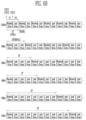
- FIG. 1 is a block diagram illustrating a display device in accordance with exemplary embodiments of the present invention.
- FIG. 2 is a circuit diagram illustrating a pixel included in the display device of FIG. 1 , according to an exemplary embodiment of the present invention.
- FIG. 3 A is a timing diagram illustrating an operation of the pixel of FIG. 2 , according to an exemplary embodiment of the present invention.
- FIG. 3 B is a timing diagram illustrating an operation of the pixel of FIG. 2 , according to an exemplary embodiment of the present invention.
- FIG. 4 is a timing diagram illustrating a method of driving the display device of FIG. 1 when the display device is driven at a first driving frequency, according to an exemplary embodiment of the present invention.
- FIG. 5 is a timing diagram illustrating a method of driving the display device of FIG. 1 when the display device is driven at a second driving frequency, according to an exemplary embodiment of the present invention.
- FIG. 6 A is a timing diagram illustrating gate start pulses to be supplied, depending on the driving frequency, to an emission driver and scan drivers that are included in the display device of FIG. 1 , according to an exemplary embodiment of the present invention.
- FIG. 6 B is a diagram illustrating a method of driving the display device of FIG. 1 depending on the driving frequency, in accordance with an exemplary embodiment of the present invention.
- FIG. 7 is a circuit diagram illustrating a pixel included in the display device of FIG. 1 , according to an exemplary embodiment of the present invention.
- FIG. 8 is a circuit diagram illustrating a pixel included in the display device of FIG. 1 , according to an exemplary embodiment of the present invention.
- FIG. 9 is a circuit diagram illustrating a pixel included in the display device of FIG. 1 , according to an exemplary embodiment of the present invention.
- FIG. 10 A is a timing diagram illustrating an operation of the pixel of FIG. 9 , according to an exemplary embodiment of the present invention.
- FIG. 10 B is a timing diagram illustrating an operation of the pixel of FIG. 9 , according to an exemplary embodiment of the present invention.
- FIG. 11 is a circuit diagram illustrating a pixel included in the display device of FIG. 1 , according to an exemplary embodiment of the present invention.
- FIG. 12 is a timing diagram illustrating an operation of the pixel of FIG. 11 , according to an exemplary embodiment of the present invention.
- FIG. 13 is a block diagram illustrating a display device in accordance with exemplary embodiments of the present invention.
- FIG. 14 is a circuit diagram illustrating a pixel included in the display device of FIG. 13 , according to an exemplary embodiment of the present invention.
- FIGS. 15 A, 15 B and 15 C are timing diagrams illustrating of the operation of the pixel of FIG. 14 , according to exemplary embodiments of the present invention.
- FIG. 16 is a circuit diagram illustrating a pixel included in the display device of FIG. 1 , according to an exemplary embodiment of the present invention.
- FIGS. 17 A and 17 B are timing diagrams illustrating an operation of the pixel of FIG. 16 , according to exemplary embodiments of the present invention.
- FIG. 18 is a circuit diagram illustrating a pixel included in the display device of FIG. 1 , according to an exemplary embodiment of the present invention.
- FIGS. 19 A and 19 B are timing diagrams illustrating an operation of the pixel of FIG. 18 , according to exemplary embodiments of the present invention.
- FIG. 1 is a block diagram illustrating a display device 1000 in accordance with exemplary embodiments of the present invention.
- the display device 1000 may include a pixel unit 100 , a first scan driver 200 , a second scan driver 300 , an emission driver 400 , a data driver 500 , and a timing controller 600 .
- the display device 1000 may display images using various driving frequencies depending on driving conditions.
- the display device 1000 may adjust, depending on driving conditions, an output frequency of the second scan driver 300 and an output frequency of the data driver 500 corresponding to the output frequencies of the first and second scan drivers 200 and 300 .
- the display device 1000 may display images in response to various driving frequencies ranging from 1 Hz to 120 Hz.
- the timing controller 600 may be supplied with input image data IRGB and timing signals Vsync, Hsync, DE, and CLK from a host system such as an application processor (AP) through an interface.
- a host system such as an application processor (AP)
- AP application processor
- the timing controller 600 may generate a data driving control signal DCS, based on the input image data IRGB and the timing signals such as a vertical synchronous signal Vsync, a horizontal synchronous signal Hsync, a data enable signal DE, and a clock signal CLK.
- the data driving control signal DCS may be supplied to the data driver 500 .
- the timing controller 600 may rearrange the input image data IRGB and supply the rearranged input image data IRGB to the data driver 500 .
- the timing controller 600 may supply gate start pulses GSP 1 and GSP 2 and clock signals CLK to the first scan driver 200 and the second scan driver 300 based on the timing signals.
- the timing controller 600 may supply an emission start pulse ESP and clock signals CLK to the emission driver 400 , based on the timing signals.
- the emission start pulse ESP may control a first timing of an emission control signal.
- the clock signals CLK provided to the emission driver 400 may be used to shift the emission start pulse.
- a first gate start pulse GSP 1 may control a first timing of a scan signal to be supplied from the first scan driver 200 .
- the clock signals CLK provided to the first scan driver 200 may be used to shift the first gate start pulse GSP 1 .
- a second gate start pulse GSP 2 may control a first timing of a scan signal to be supplied from the second scan driver 300 .
- the clock signals CLK provided to the second scan driver 300 may be used to shift the second gate start pulse GSP 2 .
- the data driver 500 may supply data signals to data lines D in response to the data driving control signal DCS.
- the data signals supplied to the data lines D may be supplied to pixels PXL selected by scan signals.
- the data driver 500 may supply data signals to the data lines D during a frame period in response to a driving frequency.
- the data driver 500 may supply data signals to the data lines D during a frame period when the display device 1000 is driven at a first driving frequency.
- the data signals to be supplied to the data lines D may be synchronized with scan signals to be supplied to first scan lines S 1 and second scan lines S 2 .
- the data driver 500 may supply data signals to the data lines D during a first period in which scan signals are supplied to the second scan lines S 2 during a single frame period, and may supply an arbitrary reference voltage to the data lines D during a second period, but not the first period.
- the reference voltage may be set to a specific voltage within a voltage range of data signals.
- the reference voltage may be set to a data voltage having a black gray scale.
- the reference voltage may be changed within the voltage range of the data signals.
- the first period may be a period in which scan signals are supplied to all of the first scan lines S 1 and the second scan lines S 2 .
- the second period may be a period in which scan signals are supplied to the first scan lines S 1 , but not the second scan lines S 2 .
- the first scan driver 200 may supply scan signals to the first scan lines S 1 in response to the first gate start pulse GSP 1 .
- the first scan driver 200 may sequentially supply scan signals to the first scan lines S 1 .
- a scan signal to be supplied from the first scan driver 200 may be set to a gate-on voltage so that a transistor included in the pixel PXL may be turned on.
- the first scan driver 200 may supply scan signals to the first scan lines S 1 at a constant first frequency regardless of a driving frequency of an image frame (or a frame frequency) of the display device 1000 .
- the first frequency may correspond to an output frequency of the first gate start pulse GSP 1 to be supplied from the timing controller 600 to the first scan driver 200 .
- the first frequency at which the first scan driver 200 supplies the scan signals may be greater than the driving frequency.
- the driving frequency may be set to a submultiple of the first frequency.
- the first frequency may be set to approximately twice the maximum driving frequency of the display device 1000 .
- the maximum driving frequency of the display device 1000 is approximately 120 Hz
- the first frequency may be set to 240 Hz. Therefore, in each frame period, a plurality of scanning operations of sequentially outputting scan signals to the first scan lines S 1 may be repeated at a predetermined cycle. In other words, in each frame period, scan signals to be supplied to the respective first scan lines S 1 may be repeatedly supplied at each predetermined cycle.
- the first scan driver 200 may perform a scanning operation once during a first period, and perform a scanning operation at least once depending on the driving frequency during a second period.
- scan signals are sequentially output once to the respective first scan lines S 1 .
- scan signals may be sequentially output at least once to the respective first scan lines S 1 .
- the scan signals may be sequentially output two or more times to the respective first scan lines S 1 .
- the number of times the first scan driver 200 repeatedly performs supplying scan signals to the respective first scan lines S 1 during each frame period may be increased.
- the second scan driver 300 may supply scan signals to the second scan lines S 2 in response to the second gate start pulse GSP 2 .
- the second scan driver 300 may sequentially supply scan signals to the second scan lines S 2 .
- a scan signal to be supplied from the second scan driver 300 may be set to a gate-on voltage so that a transistor included in the pixel PXL may be turned on.
- the second scan driver 300 may supply scan signals to the second scan lines S 2 at a frequency (e.g., a second frequency) equal to the driving frequency corresponding to the image frame (or the frame frequency) of the display device 1000 .
- the second frequency may correspond to an output frequency of the second gate start pulse GSP 2 to be supplied from the timing controller 600 to the second scan driver 300 .
- the second frequency which is substantially the same as the driving frequency, may be set to a submultiple of the first frequency.
- the second scan driver 300 may supply scan signals to the second scan lines S 2 during a first period of each frame.
- the second scan driver 300 may supply at least one scan signal to each of the second scan lines S 2 during the first period.
- a scan signal to be supplied to an i-th first scan line S 1 i during the first period may overlap with a scan signal to be supplied to an i-th second scan line S 2 i.
- the emission driver 400 may supply emission control signals to emission control lines E in response to the emission start pulse ESP. For example, the emission driver 400 may sequentially supply the emission control signals to the emission control lines E. If the emission control signals are sequentially supplied to the emission control lines E, the pixels PXL may be not-emitted on a horizontal line basis. In other words, the pixels PXL may not emit light. For this operation, the emission control signal may be set to a gate-off voltage so that transistors included in the pixels PXL may be turned off.
- the emission driver 400 may supply an emission control signal to an i-th emission control line Ei such that the emission control signal overlaps with scan signals supplied to an i ⁇ 1-th first scan line S 1 i ⁇ 1 (and/or an i ⁇ 1-th second scan line S 2 i ⁇ 1, an i-th first scan line S 1 i (and/or an i-th second scan line S 2 i ), and an i+1-th first scan line S 1 i +1 (and/or an i+1-th second scan lines S 2 i+ 1).
- the emission driver 400 may supply emission control signals to the emission control lines E at the first frequency. Hence, in each frame period, emission control signals to be supplied to the respective emission control lines E may be repeatedly supplied at each cycle.
- the number of times the emission driver 400 repeatedly performs an operation of supplying emission control signals to the respective emission control lines E during each frame period may be increased.
- the pixel unit 100 may include pixels PXL which are coupled with the data lines D, the first and second scan lines S 1 and S 2 , and the emission control lines E.
- the pixels PXL may be supplied with voltages of a first power supply VDD, a second power supply VSS, and an initialization power supply Vint from external devices.
- Each pixel PXL may be selected when a scan signal is supplied to the first and second scan lines S 1 and S 2 coupled with the pixel PXL, and when a data signal is supplied to the data line D connected with the pixel PXL.
- the pixel PXL supplied with the data signal may control, in response thereto, the amount of current flowing from the first power supply VDD to the second power supply VSS via a light emitting element.
- the light emitting element may generate light having a luminance in response to the amount of current.
- the light generated by the light emitting element may be predetermined.
- the time for which each pixel PXL emits light may be controlled by an emission control signal supplied from the emission control line E coupled with the pixel PXL.
- the pixels PXL may be coupled to one or more first scan lines S 1 , one or more second scan lines S 2 , and one or more emission control lines E depending on the structure of a pixel circuit.
- signal lines such as the first and second scan lines S 1 and S 2 , the emission control lines E, and the data lines D to be coupled to the pixel PXL may be variously arranged depending on the circuit structure of the pixel PXL.
- FIG. 2 is a circuit diagram illustrating a pixel PXL included in the display device 1000 of FIG. 1 , according to an exemplary embodiment of the present invention.
- FIG. 2 for the sake of description, there is illustrated a pixel PXL that is disposed on an i-th horizontal line and coupled with an m-th data line Dm.
- the pixel PXL may include a light emitting element LD, first, second, third, fourth, fifth, sixth and seventh transistors M 1 , M 2 , M 3 , M 4 , M 5 , M 6 and M 7 , and a storage capacitor Cst.
- the light emitting element LD may include a first electrode (either an anode electrode or a cathode electrode) coupled to a fourth node N 4 , and a second electrode (the other one of the cathode electrode and the anode electrode) coupled to the second power supply VSS.
- the light emitting element LD may emit light having a predetermined luminance corresponding to a current supplied from the first transistor M 1 .
- the light emitting element LD may be an organic light emitting diode including an organic light emitting layer.
- the light emitting element LD may be an inorganic light emitting element formed of inorganic material.
- the light emitting element LD may have a shape in which a plurality of inorganic light emitting elements are coupled in parallel and/or series between the second power supply VSS and the fourth node N 4 .
- the first transistor (or a driving transistor) M 1 may include a first electrode coupled to a first node N 1 , and a second electrode coupled to a third node N 3 .
- a gate electrode of the first transistor M 1 is coupled to a second node N 2 .
- the first transistor M 1 may control, in response to the voltage of the second node N 2 , the amount of current flowing from the first power supply VDD to the second power supply VSS via the light emitting element LD.
- the first power supply VDD may be set to a voltage higher than the second power supply VSS.
- the second transistor M 2 may be coupled between the data line Dm and the first node N 1 .
- a gate electrode of the second transistor M 2 may be coupled to the i-th first scan line S 1 i .
- the second transistor M 2 may be turned on to electrically couple the data line Dm with the first node N 1 .
- the third transistor M 3 may be coupled between the second electrode (e.g., the third node N 3 ) of the first transistor M 1 and the second node N 2 .
- a gate electrode of the third transistor M 3 may be coupled to the i-th second scan line S 2 i .
- the third transistor M 3 may be turned on to electrically connect the second electrode of the first transistor M 1 to the second node N 2 . Therefore, if the third transistor M 3 is turned on, the first transistor M 1 may be connected in the form of a diode.
- the fourth transistor M 4 is coupled between the second node N 2 and a first initialization power supply Vint 1 .
- a gate electrode of the fourth transistor M 4 is coupled to the i ⁇ 1-th second scan line S 2 i ⁇ 1.
- the fourth transistor M 4 is turned on so that the voltage of the first initialization power supply Vint 1 may be supplied to the second node N 2 .
- the voltage of the first initialization power supply Vint 1 is set to a voltage lower than a data signal to be supplied to the data line Dm.
- the gate voltage of the first transistor M 1 may be initialized to the voltage of the first initialization power supply Vint 1 , and the first transistor M 1 may have an on-bias state (e.g., the first transistor M 1 may be initialized to an on-bias state).
- the fifth transistor M 5 is coupled between the first power supply VDD and the first node N 1 .
- a gate electrode of the fifth transistor M 5 may be coupled to the emission control line Ei.
- the fifth transistor M 5 may be turned off when an emission control signal is supplied to the emission control line Ei, and may be turned on in the other cases.
- the sixth transistor M 6 may be coupled between the second electrode (e.g., the third node N 3 ) of the first transistor M 1 and the first electrode (e.g., the fourth node N 4 ) of the light emitting element LD.
- a gate electrode of the sixth transistor M 6 may be coupled to the emission control line Ei.
- the sixth transistor M 6 may be turned off when an emission control signal is supplied to the emission control line Ei, and may be turned on in the other cases.
- the seventh transistor M 7 may be coupled between the first electrode (e.g., the fourth node N 4 ) of the light emitting element LD and a second initialization power supply Vint 2 .
- a gate electrode of the seventh transistor M 7 may be coupled to the i+1-th first scan line S 1 i +1.
- the seventh transistor M 7 is turned on so that the voltage of the second initialization power supply Vint 2 may be supplied to the first electrode of the light emitting element LD.
- the gate electrode of the seventh transistor M 7 may be coupled to the i ⁇ 1-th first scan line S 1 i ⁇ 1 or the i-th first scan line S 1 i.
- a parasitic capacitor of the light emitting element LD may be discharged. As a residual voltage charged into the parasitic capacitor is discharged (e.g., removed), an undesired fine emission may be prevented. Therefore, the black expression performance of the pixel PXL may be enhanced.
- the first initialization power supply Vint 1 and the second initialization power supply Vint 2 may generate different voltages.
- a voltage (e.g., the first initialization power supply Vint 1 ) of initializing the second node N 2 and a voltage (e.g., the second initialization power supply Vint 2 ) of initializing the fourth node N 4 may be set to different values.
- the voltage of the first initialization power supply Vint 1 supplied to the second node N 2 may excessively vary during the frame period. Such hysteresis may cause a flicker phenomenon in the low-frequency driving mode. Therefore, in the low-frequency driving mode of the display device 1000 , the voltage of the first initialization power supply Vint 1 may be higher than the voltage of the second power supply VSS.
- the voltage of the second initialization power supply Vint 2 supplied to the fourth node N 4 is higher than a predetermined reference value, the voltage of the parasitic capacitor of the light emitting element LD may be charged rather than discharged. Therefore, the voltage of the second initialization power supply Vint 2 is to be lower than the voltage of the second power supply VSS.
- the pixels PXL included in the display device 1000 may be coupled with the first initialization power supply Vint 1 and the second initialization power supply Vint 2 that provide different voltages. Therefore, since a voltage of initializing the first transistor M 1 and a voltage of initializing the light emitting element LD are independently determined, a flicker phenomenon or emission error may be prevented or mitigated.
- the storage capacitor Cst may be coupled between the first power supply VDD and the second node N 2 .
- the storage capacitor Cst may store a voltage applied to the second node N 2 .
- the first transistor M 1 , the second transistor M 2 , the fifth transistor M 5 , the sixth transistor M 6 , and the seventh transistor M 7 each may be formed of a poly-silicon semiconductor transistor.
- the first transistor M 1 , the second transistor M 2 , the fifth transistor M 5 , the sixth transistor M 6 , and the seventh transistor M 7 each may include, as an active layer (e.g., a channel), a poly-silicon semiconductor layer formed through a low temperature poly-silicon (LTPS) process.
- the first transistor M 1 , the second transistor M 2 , the fifth transistor M 5 , the sixth transistor M 6 , and the seventh transistor M 7 each may be a P-type transistor. Therefore, a gate-on voltage for turning on the first transistor M 1 , the second transistor M 2 , the fifth transistor M 5 , the sixth transistor M 6 , or the seventh transistor M 7 may have a logic low level.
- the poly-silicon semiconductor transistor may be applied in a switching element in which a high-speed switching operation is employed.
- the third and fourth transistors M 3 and M 4 each may be formed of an oxide semiconductor transistor.
- each of the third and fourth transistors M 3 and M 4 may be an N-type oxide semiconductor transistor, and include an oxide semiconductor layer as an active layer.
- a gate-on voltage for turning on the third or fourth transistor M 3 or M 4 may have a logic high level.
- An oxide semiconductor transistor may be produced through a low-temperature process, and have low charge mobility compared to that of the poly-silicon semiconductor transistor. In other words, the oxide semiconductor transistor may have excellent off-current characteristics. Therefore, if each of the third transistor M 3 and the fourth transistor M 4 is formed of an oxide semiconductor transistor, leakage current from the second node N 2 may be minimized. Therefore, the display quality of the display device 1000 may be enhanced.
- FIG. 3 A is a timing diagram illustrating an operation of the pixel PXL of FIG. 2 , according to an exemplary embodiment of the present invention.
- the pixel PXL may be supplied with signals for displaying an image during a first period.
- the first period may include a period in which a data signal DS substantially corresponding to an output image is input.
- a gate-on voltage of a scan signal to be supplied to each of the second scan lines S 2 i and S 2 i ⁇ 1 coupled to the third and fourth transistors M 3 and M 4 each of which is an N-type transistor may have a logic high level.
- a gate-on voltage of a scan signal to be supplied to each of the first scan lines S 1 i and S 1 i +1 coupled to the first, second, fifth, sixth, and seventh transistors M 1 , M 2 , M 5 , M 6 , and M 7 each of which is a P-type transistor may have a logic low level.
- An emission control signal is supplied to the emission control line Ei. If the emission control signal is supplied to the emission control line Ei, the fifth and sixth transistors M 5 and M 6 may be turned off. If the fifth and sixth transistors M 5 and M 6 are turned off, the pixel PXL may be set to a non-emission state. In other words, the pixel PXL may not emit light when the fifth and sixth transistors M 5 and M 6 are turned off.
- a scan signal is supplied to the i ⁇ 1-th second scan line S 2 i ⁇ 1.
- the fourth transistor M 4 may be turned on.
- the voltage of the first initialization power source Vint 1 is supplied to the second node N 2 .
- scan signals are supplied to the i-th first scan line S 1 i and the i-th second scan line S 2 i .
- the third transistor M 3 may be turned on.
- the first transistor M 1 may be connected in the form of a diode, and the threshold voltage of the first transistor M 1 may be compensated.
- the second transistor M 2 When a scan signal is supplied to the i-th first scan line S 1 i , the second transistor M 2 may be turned on. When the second transistor M 2 is turned on, a data signal DS may be supplied from the data line Dm to the first node N 1 . In this case, since the second node N 2 has been initialized to the voltage of the first initialization power Vint 1 that is lower than the data signal DS (e.g., the second node N 2 has been initialized to an on-bias state), the first transistor M 1 may be turned on.
- the data signal DS supplied to the first node N 1 may be supplied to the second node N 2 via the first transistor M 1 that is connected in the form of a diode. Then, a voltage corresponding to the data signal DS and the threshold voltage of the first transistor M 1 may be applied to the second node N 2 .
- the storage capacitor Cst may store a voltage corresponding to the second node N 2 .
- a scan signal is supplied to the i+1-th first-scan line S 1 i +1.
- the seventh transistor M 7 may be turned on.
- the voltage of the second initialization power supply Vint 2 may be supplied to the first electrode (e.g., the fourth node N 4 ) of the light emitting element LD. Therefore, the residual voltage that remains in the parasitic capacitor of the light emitting element LD may be discharged.
- the supply of the emission control signal to the emission control line Ei may be suspended.
- the emission control signal may drop from a high level to a low level when it is suspended.
- the fifth and sixth transistors M 5 and M 6 are turned on.
- the first transistor M 1 may control a driving current flowing to the light emitting element LD in response to the voltage of the second node N 2 .
- the light emitting element LD may generate light having a luminance corresponding to the amount of current, e.g., the driving current.
- FIG. 3 A illustrates that a scan signal is supplied to each of the first and second scan lines S 1 and S 2 during the first period
- the present invention is not limited thereto.
- a plurality of scan signals may be supplied to each of the first and second scan lines S 1 and S 2 .
- an operating process is substantially the same as that of FIG. 3 A , and thus, a detailed description thereof will be omitted.
- it is assumed that a scan signal is supplied to each of the first and second scan lines S 1 and S 2 .
- the above-mentioned operation in the first period may be implemented by scan signals supplied to the second scan lines S 2 i ⁇ 1 and S 2 i , and may be synchronized with the frequency of the second scan driver 300 .
- FIG. 3 B is a timing diagram illustrating an operation of the pixel of FIG. 2 , according to an exemplary embodiment of the present invention.
- the pixel PXL may apply a predetermined reference voltage Vref to the first electrode (e.g., a source electrode) of the first transistor M 1 during the second period.
- the timing diagram of FIG. 3 B illustrates a period of the operation during the second period.
- the driving period of FIG. 3 B is a self-scan period of changing characteristics of the first transistor M 1 .
- the second period may include at least one self-scan period depending on a driving frequency.
- a scan signal is supplied to neither the third transistor M 3 nor the fourth transistor M 4 .
- a scan signal to be supplied to the i-th second scan line S 2 i and the i+1-th second scan line S 2 i+ 1 may have a logic low level L.
- the gate voltage (e.g., the second node N 2 ) of the first transistor M 1 may not be affected by an operation performed during the second period.
- an emission control signal is supplied to the emission control line Ei.
- the emission control signal goes from low to high. If the emission control signal is supplied to the emission control line Ei, the fifth and sixth transistors M 5 and M 6 are turned off. If the fifth and sixth transistors M 5 and M 6 are turned off, the pixel PXL is set to a non-emission state.
- a scan signal is supplied to the i-th first scan line S 1 i , and the second transistor M 2 may be turned on.
- the second transistor M 2 is turned on when the scan signal supplied to the i-th first scan line S 1 i goes low.
- a reference voltage Vref is supplied from the data line Dm to the first node N 1 .
- the reference voltage Vref may be set to a specific voltage within a voltage range of data signals.
- the voltage of the first node N 1 is changed from the voltage of the first power supply VDD to another voltage, and a characteristic curve of the first transistor M 1 may be changed. Therefore, after the first period in which the data signal DS is supplied has passed, a variation in luminance due to hysteresis of the first transistor M 1 may be mitigated.
- the driving frequency e.g., the frequency of driving the second scan line S 2
- the driving frequency e.g., the frequency of driving the second scan line S 2
- the characteristics of the first transistor M 1 are fixed in a specific state during each frame period, a flicker phenomenon may occur due to hysteresis characteristics.
- the reference voltage Vref is supplied to the first electrode (e.g., the source electrode) of the first transistor M 1 during the second period, the first transistor M 1 enters an on-bias state, and the characteristics of the first transistor M 1 may be changed. Consequently, the characteristics of the first transistor M 1 may be prevented from being fixed in a specific state and thus deteriorated.
- the reference voltage Vref may be periodically supplied to the first electrode of the first transistor M 1 by the first scan driver 200 .
- a scan signal is supplied to the i+1-th first-scan line S 1 i +1.
- the seventh transistor M 7 may be turned on.
- the voltage of the second initialization power supply Vint 2 may be supplied to the first electrode (e.g., the fourth node N 4 ) of the light emitting element LD. Thereby, the residual voltage that remains in the parasitic capacitor of the light emitting element LD may be discharged.
- the supply of the emission control signal to the emission control line Ei may be suspended. If the supply of the emission control signal to the emission control line Ei is suspended, the fifth and sixth transistors M 5 and M 6 are turned on. In this case, the first transistor M 1 may control a driving current flowing to the light emitting element LD in response to the voltage of the second node N 2 .
- the light emitting element LD may generate light having a luminance corresponding to the amount of the driving current.
- the above-mentioned operation in the second period may be implemented by scan signals supplied to the first scan lines S 1 i and S 1 i +1, and may be synchronized with the frequency of the first scan driver 200 .
- FIG. 4 is a timing diagram illustrating a method of driving the display device 1000 of FIG. 1 when the display device 1000 is driven at a first driving frequency, according to an exemplary embodiment of the present invention.
- the first driving frequency may be a maximum driving frequency that can be implemented by the display device 1000 .
- the first driving frequency may be set to a high frequency of 120 Hz or more.
- the first driving frequency may pertain to a cycle in which data signals DS are supplied to the data lines D.
- Each frame period 1 F may correspond to a supply cycle of data signals DS and the first driving frequency.
- each frame period 1 F may include a first period P 1 and a second period P 2 .
- the length of the first period P 1 may be substantially the same as that of the second period P 2 .
- the first scan driver 200 may sequentially supply scan signals to the first scan lines S 11 to S 1 n at a first frequency.
- the emission driver 400 may sequentially supply emission control signals to the emission control lines E 1 to En at the first frequency.
- the first frequency may be approximately double the first driving frequency.
- the second scan driver 30 may sequentially supply scan signals to the second scan lines S 21 to S 2 n at a second frequency equal to the first driving frequency.
- a scan signal supplied to an i-th first scan line S 1 i may overlap with a scan signal supplied to an i-th second scan line S 2 i .
- the scan signal applied to the first scan line S 11 may overlap with the scan signal applied to the second scan line S 21 .
- emission control signals are sequentially supplied to the emission control lines E 1 to En.
- an emission control signal supplied to an i-th emission control line Ei may overlap with scan signals supplied to an i ⁇ 1-th first scan line S 1 i ⁇ 1, the i-th first scan line S 1 i , and an i+1-th first scan line S 1 i +1.
- Data signals DS are supplied to the data lines D in synchronization with the scan signals.
- voltages corresponding to the data signals DS are stored in the respective pixels PXL, and the pixels PXL may emit light based on the stored voltages.
- an emission control signal supplied to an i-th emission control line Ei may overlap with scan signals supplied to the i ⁇ 1-th first scan line S 1 i ⁇ 1, the i-th first scan line S 1 i , and the i+1-th first scan line S 1 i +1.
- the reference voltage Vref may be supplied to each of the data lines D.
- data signals DS are supplied to the data lines D only during the first period P 1 , therefore power consumption may be reduced.
- voltages corresponding to the data signals DS are stored in the respective pixels PXL, and the pixels PXL may emit light based on the stored voltages.
- a predetermined on-bias may be applied to the first transistor M 1 by a scan signal that is supplied to each of the first scan lines S 11 to S 1 n . Therefore, the hysteresis of the first transistor M 1 in the first frame period 1 F may be improved.
- the first frequency which is an output frequency of the first scan driver 200 and the emission driver 400 , is set to a value greater than the driving frequency of the display device 1000 , it is possible to support the output of images having various driving frequencies.
- the driving frequency of the display device 1000 may correspond to submultiples of the first frequency.
- FIG. 5 is a timing diagram illustrating a method of driving the display device 1000 of FIG. 1 when the display device 1000 is driven at a second driving frequency, according to an exemplary embodiment of the present invention.
- each frame period 1 F may include a first period P 1 and a second period P 2 ′.
- An operation in the first period P 1 of FIG. 5 is substantially the same as the operation in the first period P 1 described with reference to FIG. 4 ; therefore, a repetitive description thereof will be omitted.
- the first frequency may be set to approximately 240 Hz
- the second driving frequency may be set to a frequency less than 100 Hz
- the second period P 2 ′ may be longer than the first period P 1 .
- the length of the second period P 2 ′ may correspond to an integer multiple of the length of the first period P 1 .
- FIG. 5 illustrates an example in where the second driving frequency is approximately 80 Hz.
- the first scan driver 200 and the emission driver 400 may respectively drive the first scan lines S 11 to S 1 n and the emission control lines E 1 to En at the first frequency regardless of the driving frequency of the display device 1000 .
- the first frequency may remain constant.
- the second scan driver 300 may drive the second scan lines S 21 to S 2 n at the second frequency substantially equal to the second driving frequency.
- a plurality of scan signals are supplied to each of the first scan lines S 11 to S 1 n .
- the scan signals to be supplied to each of the first scan lines S 11 to S 1 n may be supplied at a predetermined cycle.
- the scan signals may be sequentially and repeatedly supplied to the first scan lines S 11 to S 1 n a plurality of times.
- the scan signals are supplied to the first scan lines S 11 to S 1 n two times, but the present invention is not limited thereto.
- the scan signals may be supplied to the first scan lines S 11 to S 1 n more than two times.
- a plurality of emission control signals are supplied to each of the emission control lines E 1 to En.
- the emission control signals may be supplied at the substantially same cycle as that of the scan signals supplied to the first scan lines S 1 to S 1 n .
- the reference voltage Vref may be supplied to each of the data lines D.
- an on-bias may be applied to the first transistor M 1 of each of the pixels PXL, periodically (e.g., at the first frequency). Therefore, in response to various driving frequencies, the hysteresis of the first transistor M 1 in the frame period 1 F may be improved.
- FIG. 6 A is a timing diagram illustrating gate start pulses to be supplied, depending on the driving frequency, to an emission driver and scan drivers that are included in the display device 1000 of FIG. 1 , according to an exemplary embodiment of the present invention.
- FIG. 6 B is a diagram illustrating a method of driving the display device depending on the driving frequency, in accordance with an exemplary embodiment of the present invention.
- the output frequency of the second gate start pulse GSP 2 may vary depending on the driving frequency.
- the pulse widths of the first and second gate pulses GSP 1 and GSP 2 may be substantially the same as each other.
- the pulse width of the emission start pulse ESP may be greater than the pulse width of the first and second gate pulses GSP 1 and GSP 2 .
- the timing controller 600 may output the emission start pulse ESP and the first gate start pulse GSP 1 at a constant frequency (e.g., the first frequency), regardless of the driving frequency.
- the output frequency of the emission start pulse ESP and the first gate start pulse GSP 1 may be set to be double the maximum driving frequency of the display device 1000 .
- the timing controller 600 may output the second gate start pulse GSP 2 at the same frequency (e.g., the second frequency) as the driving frequency.
- Each frame period of the display device 1000 may be determined by the output cycle of the second gate start pulse GSP 2 .
- the first period P 1 of FIGS. 6 A and 6 B may be a display scan period T 1 in which all of the emission start pulse ESP, the first gate start pulse GSP 1 , and the second gate start pulse GSP 2 are output.
- each of the pixels PXL may perform the operation of FIG. 3 A .
- each of the pixels PXL may store data signals DS corresponding to images to be displayed.
- the second period P 2 or P 2 ′ of FIGS. 6 A and 6 B may include at least one self-scan period T 2 in which the emission start pulse ESP and the first gate start pulse GSP 1 are output.
- each of the pixels PXL may perform the operation of FIG. 3 B .
- a predetermined reference voltage Vref may be applied to the first electrode of the first transistor M 1 of each of the pixels PXL.
- the length of the display scan period T 1 is substantially the same as that of the self-scan period T 2 .
- the number of self-scan periods T 2 included in the second period P 2 or P 2 ′ of each frame period 1 F may depend on the driving frequency.
- each frame period 1 F may include one display scan period T 1 and one self-scan period T 2 .
- the emission start pulse ESP may be supplied at the same frequency as that of the first gate start pulse GSP 1 .
- each of the pixels PXL may alternately repeat emission (e.g., display scan) and non-emission (e.g., self scan) two times during each frame period 1 F.
- each frame period 1 F may include one display scan period T 1 and two self-scan periods T 2 .
- each of the pixels PXL may alternately repeat emission and non-emission three times during each frame period 1 F.
- each frame period 1 F may include one display scan period T 1 and four self-scan periods T 2 .
- scan signals may be supplied four times to each of the first scan lines S 11 to S 1 n .
- each of the pixels PXL may alternately repeat emission and non-emission four times during each frame period 1 F
- the display device 1000 may be driven at a driving frequency of 60 Hz, 30 Hz, 24 Hz, etc. by adjusting the number of self-scan periods T 2 included in the second period P 2 or P 2 ′.
- the display device 1000 may support various image frames at frequencies corresponding to submultiples of the first frequency.
- the driving frequency is reduced, the number of self-scan period T 2 is increased.
- a predetermined on-bias may be periodically applied to the first transistor M 1 . Consequently, luminance reduction and high flicker visibility in a low-frequency driving mode may not occur or be mitigated.
- FIG. 7 is a circuit diagram illustrating a pixel PXL included in the display device 1000 of FIG. 1 , according to an exemplary embodiment of the present invention.
- the pixel PXL may include a light emitting element LD, first to seventh transistors M 1 to M 7 , and a storage capacitor Cst.
- the pixel PXL may further include an eighth transistor M 8 .
- the light emitting element LD may emit light having a predetermined luminance corresponding to current supplied from the first transistor M 1 .
- the driving method according to FIGS. 3 A and 3 B may be applied to the pixel PXL of FIG. 7 .
- the fourth transistor M 4 and the seventh transistor M 7 may be coupled to an identical initialization power supply Vint.
- the eighth transistor T 8 may be coupled between a first node N 1 and the initialization power supply Vint.
- a gate electrode of the eighth transistor M 8 is coupled to the i ⁇ 1-th second scan line S 2 i ⁇ 1.
- the gate electrode of the fourth transistor M 4 and the gate electrode of the eighth transistor M 8 are coupled in common to the i ⁇ 1-th second scan line S 2 i ⁇ 1.
- the eighth transistor M 8 When a scan signal is supplied to the i ⁇ 1-th second scan line S 2 i ⁇ 1, the eighth transistor M 8 is turned on so that the voltage of the initialization power supply Vint may be supplied to the first node N 1 .
- the eighth transistor M 8 may be controlled simultaneously with the fourth transistor M 4 .
- the eighth transistor M 8 may remain turned off during the second period P 2 .
- the voltage of a second node N 2 may be initialized (e.g., an on-bias may be applied to the second node N 2 ) by turning on the fourth transistor M 4 .
- the fourth transistor M 4 may be turned on by the same signal used to turn on the eighth transistor M 8 .
- the eighth transistor M 8 may be added without having to remove the initialization power supply Vint.
- the voltage of the initialization power supply Vint is simultaneously supplied to the first node N 1 and the second node N 2 by turning on the fourth transistor M 4 and the eighth transistor M 8 .
- the fourth and eighth transistors M 4 and M 8 are turned on, the first transistor M 1 has a relatively low gate-source voltage, and the magnitude of a bias to be applied to the first transistor M 1 is reduced. Therefore, a variation in characteristics of the first transistor M 1 due to initialization of the gate voltage of the first transistor M 1 may be minimized.
- FIG. 7 illustrates that each of the seventh and eighth transistors M 7 and M 8 is a P-type transistor, the present invention is not limited thereto.
- at least one of the seventh transistor M 7 and the eighth transistor M 8 may be an N-type oxide semiconductor transistor.
- FIG. 8 is a circuit diagram illustrating a pixel PXL included in the display device of FIG. 1 , according to an exemplary embodiment of the present invention.
- FIG. 8 the same reference numerals are used to designate the same or similar components as those of FIG. 7 , and thus, a repetitive description thereof may be omitted.
- the pixel PXL may include a light emitting element LD, first to eighth transistors M 1 to M 8 , and a storage capacitor Cst.
- the eighth transistor M 8 may be coupled between a third node N 3 and an initialization power supply Vint.
- a gate electrode of the eighth transistor M 8 is coupled to the i ⁇ 1-th second scan line S 2 i ⁇ 1.
- the eighth transistor M 8 is turned on so that the voltage of the initialization power supply Vint may be supplied to the third node N 3 .
- a voltage corresponding to the sum (Vint+Vth) of the voltage of the initialization power supply Vint and the threshold voltage may be supplied to a first node N 1 .
- the voltage of the initialization voltage Vint is supplied to the second node N 2 by turning on the fourth transistor M 4 .
- FIG. 8 illustrates that each of the seventh and eighth transistors M 7 and M 8 is a P-type transistor, the present invention is not limited thereto.
- at least one of the seventh transistor M 7 and the eighth transistor M 8 may be an N-type oxide semiconductor transistor.
- FIG. 9 is a circuit diagram illustrating a pixel PXL included in the display device 1000 of FIG. 1 according to an exemplary embodiment of the present invention
- FIG. 10 A is a timing diagram illustrating an operation of the pixel PXL of FIG. 9 according to an exemplary embodiment of the present invention
- FIG. 10 B is a timing diagram illustrating an operation of the pixel PXL of FIG. 9 according to an exemplary embodiment of the present invention.
- the pixel PXL may include a light emitting element LD, first to seventh transistors M 1 to M 7 , and a storage capacitor Cst.
- each of the third transistor M 3 , the fourth transistor M 4 , and the seventh transistor M 7 is an N-type transistor.
- each of the third transistor M 3 , the fourth transistor M 4 , and the seventh transistor M 7 may be an N-type oxide semiconductor transistor.
- the seventh transistor M 7 is an oxide semiconductor transistor, leakage current from a fourth node N 4 may be minimized, therefore the display quality of the display device 1000 may be enhanced.
- a gate electrode of the seventh transistor M 7 may be coupled to the i-th second scan line S 2 i . Therefore, the third transistor M 3 and the seventh transistor M 7 may be simultaneously turned on. Furthermore, as illustrated in FIGS. 10 A and 10 B , the width of an emission control signal to be supplied to the i-th emission control line Ei may be reduced.
- the gate electrode of the seventh transistor M 7 may be coupled to the i ⁇ 1-th second scan line S 2 i ⁇ 1 or the i+1-th second scan line S 2 i+ 1.
- a method of operating the pixel PXL is substantially the same as that of the pixel PXL of FIG. 2 .
- the main difference is that the gate electrode of the seventh transistor M 7 is coupled to the second scan line S 2 i and a point in time at which the seventh transistor M 7 is turned on differs from that of the pixel PXL of FIG. 2 . Therefore, a repetitive description thereof will be omitted.
- FIG. 11 is a circuit diagram illustrating a pixel PXL included in the display device 1000 of FIG. 1
- FIG. 12 is a timing diagram illustrating an operation of the pixel PXL of FIG. 11 , according to an exemplary embodiment of the present invention.
- the pixel PXL may include a light emitting element LD, first to seventh transistors M 1 to M 7 , and a storage capacitor Cst.
- the light emitting element LD may emit light having a predetermined luminance corresponding to current supplied from the first transistor M 1 .
- each of the third, fourth, and seventh transistors M 3 , M 4 , and M 7 is an N-type transistor.
- each of the third transistor M 3 , the fourth transistor M 4 , and the seventh transistor M 7 may be an N-type oxide semiconductor transistor.
- Each of the first, second, fifth, and sixth transistors M 1 , M 2 , M 5 , and M 6 is a P-type transistor.
- each of the first, second, fifth, and sixth transistors M 1 , M 2 , M 5 , and M 6 may be a P-type LTPS transistor.
- the seventh transistor M 7 is coupled between a second initialization power supply Vint 2 and a fourth node N 4 .
- a gate electrode of the seventh transistor M 7 may be coupled to the i-th emission control line Ei.
- the seventh transistor M 7 may be turned on when an emission control signal is supplied to the emission control line Ei, and may be turned off in the other cases.
- the seventh transistor M 7 that is an N-type transistor may be turned on or off contrary to the fifth and sixth transistors M 5 and M 6 . For example, when the seventh transistor M 7 is on, the fifth and sixth transistors M 5 and M 6 are off.
- the seventh transistor M 7 When an emission control signal is supplied, the seventh transistor M 7 is turned on so that the voltage of the second initialization power supply Vint 2 may be supplied to the first electrode of the light emitting element LD.
- Signals to be supplied to the pixel PXL during the first period P 1 are substantially the same as those of the driving method described with reference to FIG. 10 A ; therefore, a repetitive description thereof will be omitted.
- only an emission control signal may be supplied to the pixel PXL through the i-th emission control line Ei during the second period P 2 (e.g., the self-scan period T 2 ).
- a scan signal is supplied to neither the first scan line S 1 nor the second scan line S 2 .
- a gate off voltage having a logic high level H may be supplied to the first scan line S 1 (e.g., S 1 i ).
- a gate off voltage having a logic low level L may be supplied to the second scan line S 2 (e.g., S 2 i ⁇ 1 and S 2 i ).
- the emission control signal supplied to the i-th emission control line Ei transitions from a logic low level to a logic high level. Therefore, the fifth transistor M 5 and the sixth transistor M 6 are turned off.
- the gate voltage of the fifth transistor M 5 is increased, e.g., by a parasitic capacitor between the gate electrode of the fifth transistor M 5 and the first node N 1 , the voltage of the first node N 1 is coupled with the increased gate voltage of the fifth transistor M 5 . As a consequence, the voltage of the first node N 1 may be increased. Therefore, an on-bias may be applied to the first transistor M 1 at each first time t 1 of the second period P 2 .
- the first scan driver 200 may not output a scan signal during the second period P 2 . Consequently, the power consumption may be reduced.
- FIG. 13 is a block diagram illustrating a display device 1000 in accordance with exemplary embodiments of the present invention.
- the display device 1000 may include a pixel unit 100 , a first scan driver 200 , a second scan driver 300 , a third scan driver 350 , an emission driver 400 , a data driver 500 , and a timing controller 600 ′.
- the timing controller 600 ′ may supply gate start pulses GSP 1 , GSP 2 , and GSP 3 and clock signals CLK to the first scan driver 200 , the second scan driver 300 , and the third scan driver 350 based on timing signals Vsync, Hsync, DE, and CLK.
- the first gate start pulse GSP 1 may control a first timing of a scan signal to be supplied from the first scan driver 200 .
- the second gate start pulse GSP 2 may control a first timing of a scan signal to be supplied from the second scan driver 300 .
- the third gate start pulse GSP 3 may control a first timing of a scan signal to be supplied from the third scan driver 350 .
- a pulse width of at least one of the first to third gate start pulses GSP 1 to GSP 3 may differ from that of the other. Therefore, the widths of their corresponding scan signals may also vary.
- the data driver 500 may supply data signals to data lines D in response to a data driving control signal DCS.
- the data signals supplied to the data lines D may be supplied to pixels PXL selected by scan signals.
- the first scan driver 200 may supply scan signals to the first scan lines S 1 in response to the first gate start pulse GSP 1 .
- the first scan driver 200 may supply scan signals to the first scan lines S 1 at a first frequency regardless of a driving frequency of the display device 1000 .
- the first scan driver 200 may output scan signals during a first period P 1 and a second period P 2 .
- the first scan driver 200 may output scan signals during each self-scan period T 2 .
- the second scan driver 300 may supply scan signals to the second scan lines S 2 in response to the second gate start pulse GSP 2 .
- the second scan driver 300 may supply scan signals to the second scan lines S 2 at a second frequency corresponding to the driving frequency of the display device 1000 . In other words, the second scan driver 300 may output scan signals during the first period P 1 .
- the third scan driver 350 may supply scan signals to the third scan lines S 3 in response to the third gate start pulse GSP 3 .
- the third scan driver 350 may supply scan signals to the third scan lines S 3 at a second frequency corresponding to the driving frequency of the display device 1000 .
- the third scan driver 350 may output scan signals during the first period P 1 .
- the width of a scan signal output from the third scan driver 350 may differ from the width of a scan signal output from the second scan driver 300 .
- a scan signal output from the first scan driver 200 may have a gate-on voltage having a logic low level to control a P-type transistor.
- Each of scan signals output from the second and third scan drivers 300 and 350 may have a gate-on voltage having a logic high level to control an N-type transistor.
- the pixels PXL may be coupled to one or more first scan lines S 1 , one or more second scan lines S 2 , one or more third scan lines S 3 , and one or more emission control lines E depending on the structure of a pixel circuit.
- FIG. 14 is a circuit diagram illustrating a pixel PXL included in the display device 1000 of FIG. 13 according to an exemplary embodiment of the present invention
- FIGS. 15 A to 15 C are timing diagrams illustrating an operation of the pixel PXL of FIG. 14 according to exemplary embodiments of the present invention.
- FIG. 14 for the sake of description, there is illustrated a pixel PXL that is disposed on an i-th horizontal line and coupled with an m-th data line Dm.
- the pixel PXL may include a light emitting element LD, first to seventh transistors M 1 to M 7 , and a storage capacitor Cst.
- the light emitting element LD may emit light having a predetermined luminance corresponding to current supplied from the first transistor M 1 .
- each of the third, fourth, and seventh transistors M 3 , M 4 , and M 7 is an N-type transistor.
- each of the third transistor M 3 , the fourth transistor M 4 , and the seventh transistor M 7 may be an N-type oxide semiconductor transistor.
- Each of the first, second, fifth, and sixth transistors M 1 , M 2 , M 5 , and M 6 is a P-type transistor.
- each of the first, second, fifth, and sixth transistors M 1 , M 2 , M 5 , and M 6 may a P-type LTPS transistor.
- a gate electrode of the fourth transistor M 4 may be coupled to an i-th third scan line S 3 i . Therefore, in the case where the width of a scan signal supplied to the third scan line S 3 differs from that of a scan signal supplied to the second scan line S 2 , a turn-on time of the third transistor M 3 and a turn-on time of the fourth transistor M 4 may differ from each other.
- an emission control signal is supplied to the emission control line Ei. If the emission control signal is supplied to the emission control line Ei, the fifth and sixth transistors M 5 and M 6 are turned off, and the seventh transistor M 7 is turned on. If the fifth and sixth transistors M 5 and M 6 are turned off, the pixel PXL is set to a non-emission state. A second initialization power supply Vint 2 is supplied to a fourth node N 4 by turning on the seventh transistor M 7 .
- a scan signal supplied to the third scan line S 3 i may be supplied earlier than a scan signal supplied to the first scan line S 1 i or a scan signal supplied to the second scan line S 2 i . Therefore, the fourth transistor M 4 may be turned on by the scan signal supplied to the third scan line S 3 i . If the fourth transistor M 4 is turned on, the first initialization power supply Vint 1 is supplied to a second node N 2 . In this case, the first transistor M 1 has an on-bias state.
- the third transistor M 3 may be turned on by the scan signal supplied to the second scan line S 2 i .
- the first transistor M 1 may be coupled in the form of a diode.
- the scan signal supplied to the second scan line S 2 i may overlap with the scan signal supplied to the first scan line S 1 i . Furthermore, the width of the scan signal supplied to the second scan line S 2 i may be greater than the width of the scan signal supplied to the first scan line S 1 i.
- the second transistor M 2 is turned on by the scan signal supplied to the first scan line S 1 i . If the second transistor M 2 is turned on, a voltage of a data signal is supplied to the first transistor M 1 through a first node N 1 , and the state of the first transistor M 1 may be changed to an off-bias state in which the voltage of the second node N 2 is lower than the voltage of the first node N 1 . Furthermore, a data signal DS and a voltage corresponding to the threshold voltage of the first transistor M 1 may be applied to the first node N 1 by the first transistor M 1 connected in the form of a diode. In this case, the storage capacitor Cst may store a voltage corresponding to the second node N 2 .
- the second transistor M 2 and the third transistor M 3 are sequentially turned off.
- the supply of the emission control signal to the emission control line Ei may be suspended. If the supply of the emission control signal to the emission control line Ei is suspended, the fifth and sixth transistors M 5 and M 6 are turned on, and the seventh transistor M 7 is turned off. In this case, the first transistor M 1 may control a driving current flowing to the light emitting element LD in response to the voltage of the second node N 2 .
- the light emitting element LD may generate light having a luminance corresponding to the amount of current provided thereto.
- each of the scan signals supplied to the second scan line S 2 i and the third scan line S 3 i may have a width corresponding to two or more horizontal periods ( 2 H).
- Each of the second scan driver 300 and the third scan driver 350 may include a plurality of stages configured to shift and output scan signals.
- the output of each stage included in the second scan driver 300 may share two or more consecutive second scan lines S 2 .
- an identical scan signal may be supplied from the second scan driver 300 to an i-th horizontal line and an i+1-th horizontal line at the same time.
- the number of stages included in the second scan driver 300 may be reduced to half of the number of stages included in the first scan driver 200 . Therefore, the production cost of the display device 1000 may be reduced.
- a scan signal supplied to the second scan line S 2 i may overlap with a scan signal supplied to the first scan line S 1 i and a scan signal to be supplied to the third scan line S 3 i .
- the width of the scan signal supplied to the second scan line S 2 i may be greater than the width of the scan signal supplied to the first scan line S 1 i or the third scan line S 3 i.
- the third and fourth transistors M 3 and M 4 are turned on. If the third and fourth transistors M 3 and M 4 are turned on, the first initialization voltage Vint 1 is supplied to the second and third nodes N 2 and N 3 . Furthermore, if the third and fourth transistors M 3 and M 4 are turned on, the first node N 1 has a voltage corresponding to the sum (Vint+Vth) of the first initialization voltage Vint 1 and the threshold voltage of the first transistor M 1 by virtue of the first transistor M 1 being connected in the form of a diode. Therefore, the first transistor M 1 has an off-bias state.
- a subsequent driving method is substantially the same as the driving method of FIG. 15 A ; therefore, a further explanation thereof will be omitted.
- an emission control signal is supplied to the emission control line Ei during a self-scan period T 2 included in the second period P 2 .
- the light emitting element LD is periodically initialized during the second period P 2 .
- a scan signal is supplied to the first scan line S 1 i during the self-scan period T 2 . Therefore, a predetermined voltage is periodically applied to a first electrode (e.g., a source electrode) of the first transistor M 1 during the second period P 2 .
- a driving method of the embodiment of FIG. 15 C is substantially the same as the driving method described with reference to FIG. 3 B , etc., therefore; a further explanation thereof will be omitted.
- the driving method of the pixel PXL described with reference to FIGS. 15 A to 15 C may also be applied to the pixel PXL described with reference to FIGS. 2 , 9 , 11 , etc. in substantially the same manner.
- FIG. 16 is a circuit diagram illustrating a pixel PXL included in the display device 1000 of FIG. 1
- FIGS. 17 A and 17 B are timing diagrams illustrating an operation of the pixel PXL of FIG. 16 , according to an exemplary embodiment of the present invention.
- FIGS. 16 to 17 B the same reference numerals are used to designate the same or similar components as those of FIGS. 2 to 3 B , and thus, a repetitive description thereof may be omitted.
- the pixel PXL may include a light emitting element LD, first to seventh transistors M 1 to M 7 , and a storage capacitor Cst.
- each of the first to seventh transistors M 1 to M 7 is a poly-silicon semiconductor transistor.
- each of the first to seventh transistors M 1 to M 7 may be a P-type LTPS transistor.
- each of scan signals to be supplied to the first to seventh transistors M 1 to M 7 has a gate-on voltage having a logic low level.
- a driving method illustrated in FIG. 17 A pertains to an operation of the pixel PXL during the first period P 2 (e.g., the display scan period T 1 ).
- a driving method illustrated in FIG. 17 B pertains to an operation of the pixel PXL during the self-scan period T 2 of the second period P 2 .
- the driving methods of FIGS. 17 A and 17 B are substantially the same as the driving method of FIGS. 3 A and 3 B ; therefore, a repetitive description thereof will be omitted.
- the main difference is that in the methods of FIGS. 17 A and 17 B , a scan signal has a gate-on voltage having a logic low level.
- FIG. 18 is a circuit diagram illustrating a pixel PXL included in the display device 1000 of FIG. 1 according to an exemplary embodiment of the present invention
- FIGS. 19 A and 19 B are timing diagrams illustrating an operation of the pixel PXL of FIG. 18 according to an exemplary embodiment of the present invention.
- the pixel PXL may include a light emitting element LD, first to sixth transistors M 1 ′ to M 6 ′, and a storage capacitor Cst.
- the first to sixth transistors M 1 ′ and M 6 ′ each may be an oxide semiconductor transistor.
- the first to sixth transistors M 1 ′ and M 6 ′ each may be an N-type oxide semiconductor transistor.
- the light emitting element LD may emit light having a predetermined luminance corresponding to current supplied from the first transistor M 1 .
- the first transistor M 1 ′ (or the driving transistor) is connected between a first node N 1 and a third node N 3 .
- a gate electrode of the first transistor M 1 is coupled to a second node N 2 .
- the first transistor M 1 may control, in response to the voltage of the second node N 2 , the amount of current flowing from the first power supply VDD to the second power supply VSS via the light emitting element LD.
- the second transistor M 2 ′ may be coupled between a data line Dm and a fourth node N 4 .
- a gate electrode of the second transistor M 2 ′ may be coupled to an i-th first scan line S 1 i .
- the second transistor M 2 ′ may be turned on to electrically couple the data line Dm with the fourth node N 4 .
- the third transistor M 3 ′ is coupled between the first node N 1 and the second node N 2 .
- a gate electrode of the third transistor M 3 ′ may be coupled to an i-th second scan line S 2 i.
- the fourth transistor M 4 ′ is coupled between the first power supply VDD and the first node N 1 .
- a gate electrode of the fourth transistor M 4 ′ is coupled to an i-th emission control line Ei.
- the fourth transistor M 4 ′ may be turned off when an emission control signal is supplied to the i-th emission control line Ei, and may be turned on in the other cases.
- the fifth transistor M 5 ′ is coupled between the third node N 3 and the fourth node N 4 .
- a gate electrode of the fifth transistor M 5 ′ may be coupled to an i ⁇ 1-th emission control line Ei ⁇ 1.
- the fifth transistor M 5 ′ may be turned off when an emission control signal is supplied to the i ⁇ 1-th emission control line Ei ⁇ 1, and may be turned on in the other cases.
- the sixth transistor M 6 ′ may be coupled between the third node N 3 and an initialization power supply Vint.
- a gate electrode of the sixth transistor M 6 ′ may be coupled to the i-th first scan line S 1 i.
- the storage capacitor Cst may be coupled between the second node N 2 and the fourth node N 4 .
- the storage capacitor Cst may store a voltage applied to the fourth node N 4 .
- FIG. 19 A illustrates an example of a driving method during the first period P 1 .
- an emission control signal is supplied to the i ⁇ 1-th emission control line Ei ⁇ 1, and the fifth transistor M 5 ′ is turned off.
- the sixth transistor M 6 ′ since the sixth transistor M 6 ′ is in a turned-on state, the first power supply VDD is supplied to the first node N 1 .
- scan signals are supplied to the first scan line S 1 i and the second scan line S 2 i , and the second, third, and sixth transistors M 2 ′, M 3 ′, and M 6 ′ are turned on.
- the second transistor M 2 ′ If the second transistor M 2 ′ is turned on, a data signal DS is supplied to the fourth node N 4 . If the third transistor M 3 ′ is turned on, the voltage of the first power supply VDD is supplied to the second node N 2 . Hence, the first transistor M 1 ′ may have an off-bias state. If the sixth transistor M 6 ′ is turned on, the voltage of the initialization power supply Vint is supplied to the third node N 3 (e.g., the first electrode of the light emitting element LD).
- the third node N 3 e.g., the first electrode of the light emitting element LD.
- the first node N 1 and the second node N 2 may have a voltage corresponding to the sum (Vint+Vth) of the voltage of the initialization power supply Vint and the threshold voltage of the first transistor M 1 ′. In other words, the threshold voltage of the first transistor M 1 ′ may be compensated for.
- the supply of the emission control signal to the i ⁇ 1-th emission control line Ei ⁇ 1 is suspended, and the fifth transistor M 5 ′ is turned on. If the fifth transistor M 5 ′ is turned on, the voltage of the initialization power supply Vint of the third node N 3 is transmitted to the fourth node N 4 .
- the sum (DS+Vth) of the data signal DS and the threshold voltage of the first transistor M 1 ′ is transmitted to the second node N 2 by coupling.
- a voltage corresponding to Vth+DS ⁇ Vint is stored in the storage capacitor Cst.
- the pixel PXL may emit light based on the voltage corresponding to Vth+DS ⁇ Vint.
- an operation of compensating for the threshold voltage of the first transistor M 1 ′ and a data write operation may be separated from each other. Accordingly, the time required for the threshold voltage compensation may be reliably secured.
- FIG. 19 B illustrates an example of a driving method during the self-scan period T 2 of the second period P 2 .
- a scan signal is not supplied to the second scan line S 2 i during the second period P 2 .
- the third transistor M 3 ′ is not turned on during the second period P 2 .
- a predetermined reference voltage Vref may be supplied to the fourth node N 4 by turning on the second transistor M 2 ′, and the light emitting element LD may be initialized by turning on the sixth transistor M 6 ′.
- the scan signal to be supplied to the first scan line S 1 i and the emission control signals to be supplied to the emission control lines Ei ⁇ 1 and Ei may be supplied at the first frequency regardless of the driving frequency.
- the scan signal to be supplied to the second scan line S 2 i may be supplied to the second scan line S 2 i at the second frequency corresponding to the driving frequency.
- the driving frequency of the display device 1000 may correspond to submultiples of the first frequency.
- each frame period includes a display scan period and at least one self-scan period, so that the output of images having various driving frequencies can be supported. Furthermore, as a driving frequency is reduced, the number of self-scan periods is increased. Consequently, luminance reduction and high flicker visibility in a low-frequency driving mode may not occur or be mitigated.
- a predetermined bias is periodically applied to a first transistor (e.g., a driving transistor)
- the power consumption may be reduced, and a flicker phenomenon in the low-frequency driving mode may be mitigated.
Landscapes
- Engineering & Computer Science (AREA)
- Physics & Mathematics (AREA)
- Computer Hardware Design (AREA)
- General Physics & Mathematics (AREA)
- Theoretical Computer Science (AREA)
- Control Of Indicators Other Than Cathode Ray Tubes (AREA)
- Control Of El Displays (AREA)
Abstract
A display device including: pixels coupled to first scan lines, second scan lines, emission control lines, and data lines; a first scan driver configured to supply a first scan signal to each of the first scan lines at a first frequency; a second scan driver configured to supply a second scan signal to each of the second scan lines at a second frequency corresponding to a driving frequency of the pixels; an emission driver configured to supply an emission control signal to each of the emission control lines at the first frequency; a data driver configured to supply a data signal to each of the data lines at the second frequency; and a timing controller configured to control the first scan driver, the second scan driver, the emission driver, and the data driver.
Description
The present application is a continuation of U.S. patent application Ser. No. 17/340,482 filed on Jun. 7, 2021, which is a continuation of U.S. patent application Ser. No. 16/823,894 filed on Mar. 19, 2020, now U.S. Pat. No. 11,056,060 issued on Jul. 6, 2021, which claims priority under 35 U.S.C. § 119 to Korean patent application no. 10-2019-0069638 filed on Jun. 12, 2019, the disclosures of which are incorporated by reference herein in their entireties.
Exemplary embodiments of the present invention relate to a display device, and more particularly, to a display device which may be applied to various driving frequencies.
A display device can function as an interface between a user and information.
The display device may include a plurality of pixels. Each of the pixels may include a plurality of transistors, a light emitting element electrically coupled to the transistors, and a capacitor. The transistors may be turned on in response to signals provided through lines such as scan lines and emission control lines. When the transistors are activated, a driving current may be generated to cause the light emitting element to emit light.
In an effort to reduce power consumption and enhance driving efficiency, a method of driving display devices with low frequencies may be employed. However, there may be a drop off in the display quality of the display devices that are operated at low frequencies.
An exemplary embodiment of the present invention may provide a display device including: pixels coupled to first scan lines, second scan lines, emission control lines, and data lines; a first scan driver configured to supply a first scan signal to each of the first scan lines at a first frequency; a second scan driver configured to supply a second scan signal to each of the second scan lines at a second frequency corresponding to a driving frequency of the pixels; an emission driver configured to supply an emission control signal to each of the emission control lines at the first frequency; a data driver configured to supply a data signal to each of the data lines at the second frequency; and a timing controller configured to control operations of the first scan driver, the second scan driver, the emission driver, and the data driver.
In an exemplary embodiment of the present invention, the first frequency may be greater than the second frequency.
In an exemplary embodiment of the present invention, the second frequency is equal to the driving frequency and the second frequency and the driving frequency may correspond to a submultiple of the first frequency.
In an exemplary embodiment of the present invention, the first scan driver may supply the first scan signal to each of the first scan lines at the first frequency that is two times a maximum driving frequency of the display device.
In an exemplary embodiment of the present invention, the emission driver may supply the emission control signal to each of the emission control lines at the first frequency that is two times the maximum driving frequency of the display device.
In an exemplary embodiment of the present invention, when driven at the driving frequency, the second scan driver may supply the second scan signal during a first period of a frame period. When driven at the driving frequency, the second scan driver may not supply the second scan signal during a second period of the frame period.
In an exemplary embodiment of the present invention, when driven at the maximum driving frequency of the display device, a length of the first period may be equal to a length of the second period.
In an exemplary embodiment of the present invention, the first period may include a display scan period in which the first scan driver and the second scan driver supply the first and second scan signals so that the data signal is written to the pixels. The second period may include a self-scan period in which characteristics of a driving transistor included in each of the pixels is changed by the supply of the first scan signal from the first scan driver.
In an exemplary embodiment of the present invention, when the driving frequency is reduced, the number of self-scan periods included in the second period may be increased.
In an exemplary embodiment of the present invention, each of pixels disposed on an i-th (i is a natural number) horizontal line of the pixels may include: a light emitting element including a first electrode, and a second electrode coupled to a second power supply; a first transistor including a first electrode coupled to a first node electrically connected to a first power supply, and configured to control a driving current based on a voltage of a second node; a second transistor coupled between a data line of the data lines and the first node, and configured to be turned on by the first scan signal supplied to an i-th first scan line of the first scan lines; a third transistor coupled between the second node and a third node coupled to a second electrode of the first transistor, and configured to be turned on by the second scan signal supplied to an i-th second scan line of the second scan lines; a fourth transistor coupled between the second node and a first initialization power supply, and configured to be turned on by the second scan signal supplied to an i−1-th second scan line of the second scan lines; a fifth transistor coupled between the first power supply and the first node, and configured to be turned off by an emission control signal supplied to an i-th emission control line of the emission control lines; a sixth transistor coupled to the third node and the first electrode of the light emitting element, and configured to be turned off the emission control signal; and a storage capacitor coupled between the first power supply and the second node.
In an exemplary embodiment of the present invention, each of the pixels disposed on the i-th horizontal line may further include a seventh transistor coupled between the first electrode of the light emitting element and a second initialization power supply, and may be configured to be turned on by the first scan signal supplied to an i+1-th first scan line of the first scan lines. A voltage of the first initialization power supply may be different than a voltage of the second initialization power supply.
In an exemplary embodiment of the present invention, each of the pixels disposed on the i-th horizontal line may further include: a seventh transistor coupled between the first electrode of the light emitting element and the first initialization power supply, and configured to be turned on by the first scan signal supplied to an i+1-th first scan line of the first scan lines; and an eighth transistor coupled between the first node and the first initialization power supply, and configured to be turned on by the second scan signal supplied to the i−1-th second scan line.
In an exemplary embodiment of the present invention, each of the pixels disposed on the i-th horizontal line may further include: a seventh transistor coupled between the first electrode of the light emitting element and the first initialization power supply, and configured to be turned on by a first scan signal supplied to an i+1-th first scan line of the first scan lines; and an eighth transistor coupled between the third node and the first initialization power supply, and configured to be turned on by the second scan signal supplied to the i−1-th second scan line.
In an exemplary embodiment of the present invention, each of the first transistor, the second transistor, the fifth transistor, and the sixth transistor may be a P-type transistor. Each of the third transistor and the fourth transistor may be an N-type oxide semiconductor transistor.
In an exemplary embodiment of the present invention, each of the pixels disposed on the i-th horizontal line may further include a seventh transistor coupled between the first electrode of the light emitting element and a second initialization power supply, and may be configured to be turned on by the second scan signal supplied to the i-th second scan line. The seventh transistor may be an N-type oxide semiconductor transistor. A voltage of the first initialization power supply may be different than a voltage of the second initialization power supply.
In an exemplary embodiment of the present invention, each of the pixels disposed on the i-th horizontal line may further include a seventh transistor coupled between the first electrode of the light emitting element and the second initialization power supply, and may be configured to be turned on by the emission control signal supplied to the i-th emission control line. The seventh transistor may be an N-type oxide semiconductor transistor. The voltage of the first initialization power supply may be different than the voltage of the second initialization power supply.
In an exemplary embodiment of the present invention, each of pixels disposed on an i-th (i is a natural number) horizontal line of the pixels may include: a light emitting element including a first electrode, and a second electrode coupled to a second power supply; a first transistor including a first electrode coupled to a first node electrically connected to a first power supply, and configured to control a driving current based on a voltage of a second node; a second transistor coupled between a data line of the data lines and the first node, and configured to be turned on by the first scan signal supplied to an i-th first scan line of the first scan lines; a third transistor coupled between the second node and a third node coupled to a second electrode of the first transistor, and configured to be turned on by the second scan signal supplied to an i-th second scan line of the second scan lines; a fourth transistor coupled between the second node and a first initialization power supply, and configured to be turned on by a third scan signal supplied to an i-th third scan line; and a fifth transistor coupled between the first power supply and the first node, and configured to be turned off by the emission control signal supplied to an i-th emission control line of the emission control lines.
In an exemplary embodiment of the present invention, the display device may further include a third scan driver configured to supply a third scan signal to each of third scan lines coupled to the pixels at the second frequency. Widths of the second and the third scan signals may be greater than a width of the first scan signal.
In an exemplary embodiment of the present invention, when driven at the driving frequency, the second and the third scan drivers may respectively supply the second and third scan signals during a first period of a frame period. When driven at the driving frequency, the second and the third scan drivers may not supply the second and third scan signals during a second period of the frame period.
In an exemplary embodiment of the present invention, during the first period, the second scan signal supplied to the i-th second scan line may not overlap with the third scan signal supplied to the i-th third scan line.
In an exemplary embodiment of the present invention, during the first period, the third scan signal supplied to the i-th third scan signal may overlap with a first portion of the second scan signal supplied to the i-th second scan line, and the first scan signal supplied to the i-th first scan line may overlap with a second portion of the second scan signal supplied to the i-th second scan line.
An exemplary embodiment of the present invention may provide a display device including; pixels coupled to first scan lines, second scan lines, emission control lines, and data lines; a first scan driver configured to supply a first scan signal to each of the first scan lines at a first frequency; a second scan driver configured to supply a second scan signal to each of the second scan lines at a second frequency, wherein the first frequency is greater than the second frequency; an emission driver configured to supply an emission control signal to each of the emission control lines at the first frequency; a data driver configured to supply a data signal to each of the data lines at the second frequency; and a timing controller configured to control the second scan driver to supply the second scan signal during a first period of a frame period and not supply the second scan signal during a second period of the frame period.
Exemplary embodiments of the present invention will hereinafter be described in detail with reference to the accompanying drawings. The same reference numerals used throughout the drawings may designate the same components, and thus, repetitive descriptions of the same components may be omitted.
Referring to FIG. 1 , the display device 1000 may include a pixel unit 100, a first scan driver 200, a second scan driver 300, an emission driver 400, a data driver 500, and a timing controller 600.
The display device 1000 may display images using various driving frequencies depending on driving conditions. In an exemplary embodiment of the present invention, the display device 1000 may adjust, depending on driving conditions, an output frequency of the second scan driver 300 and an output frequency of the data driver 500 corresponding to the output frequencies of the first and second scan drivers 200 and 300. For example, the display device 1000 may display images in response to various driving frequencies ranging from 1 Hz to 120 Hz.
The timing controller 600 may be supplied with input image data IRGB and timing signals Vsync, Hsync, DE, and CLK from a host system such as an application processor (AP) through an interface.
The timing controller 600 may generate a data driving control signal DCS, based on the input image data IRGB and the timing signals such as a vertical synchronous signal Vsync, a horizontal synchronous signal Hsync, a data enable signal DE, and a clock signal CLK. The data driving control signal DCS may be supplied to the data driver 500. The timing controller 600 may rearrange the input image data IRGB and supply the rearranged input image data IRGB to the data driver 500.
The timing controller 600 may supply gate start pulses GSP1 and GSP2 and clock signals CLK to the first scan driver 200 and the second scan driver 300 based on the timing signals.
The timing controller 600 may supply an emission start pulse ESP and clock signals CLK to the emission driver 400, based on the timing signals. The emission start pulse ESP may control a first timing of an emission control signal. The clock signals CLK provided to the emission driver 400 may be used to shift the emission start pulse.
A first gate start pulse GSP1 may control a first timing of a scan signal to be supplied from the first scan driver 200. The clock signals CLK provided to the first scan driver 200 may be used to shift the first gate start pulse GSP1.
A second gate start pulse GSP2 may control a first timing of a scan signal to be supplied from the second scan driver 300. The clock signals CLK provided to the second scan driver 300 may be used to shift the second gate start pulse GSP2.
The data driver 500 may supply data signals to data lines D in response to the data driving control signal DCS. The data signals supplied to the data lines D may be supplied to pixels PXL selected by scan signals.
The data driver 500 may supply data signals to the data lines D during a frame period in response to a driving frequency. For example, the data driver 500 may supply data signals to the data lines D during a frame period when the display device 1000 is driven at a first driving frequency. In this case, the data signals to be supplied to the data lines D may be synchronized with scan signals to be supplied to first scan lines S1 and second scan lines S2.
The data driver 500 may supply data signals to the data lines D during a first period in which scan signals are supplied to the second scan lines S2 during a single frame period, and may supply an arbitrary reference voltage to the data lines D during a second period, but not the first period. For example, the reference voltage may be set to a specific voltage within a voltage range of data signals. For example, the reference voltage may be set to a data voltage having a black gray scale. Furthermore, as a horizontal period passes or a frame period passes, the reference voltage may be changed within the voltage range of the data signals.
In addition, the first period may be a period in which scan signals are supplied to all of the first scan lines S1 and the second scan lines S2. The second period may be a period in which scan signals are supplied to the first scan lines S1, but not the second scan lines S2.
The first scan driver 200 may supply scan signals to the first scan lines S1 in response to the first gate start pulse GSP1. For example, the first scan driver 200 may sequentially supply scan signals to the first scan lines S1. In this case, a scan signal to be supplied from the first scan driver 200 may be set to a gate-on voltage so that a transistor included in the pixel PXL may be turned on.
The first scan driver 200 may supply scan signals to the first scan lines S1 at a constant first frequency regardless of a driving frequency of an image frame (or a frame frequency) of the display device 1000. In this case, the first frequency may correspond to an output frequency of the first gate start pulse GSP1 to be supplied from the timing controller 600 to the first scan driver 200.
Furthermore, the first frequency at which the first scan driver 200 supplies the scan signals may be greater than the driving frequency. In an exemplary embodiment of the present invention, the driving frequency may be set to a submultiple of the first frequency. For example, the first frequency may be set to approximately twice the maximum driving frequency of the display device 1000. In the case where the maximum driving frequency of the display device 1000 is approximately 120 Hz, the first frequency may be set to 240 Hz. Therefore, in each frame period, a plurality of scanning operations of sequentially outputting scan signals to the first scan lines S1 may be repeated at a predetermined cycle. In other words, in each frame period, scan signals to be supplied to the respective first scan lines S1 may be repeatedly supplied at each predetermined cycle.
For example, at all driving frequency conditions at which the display device 1000 may be driven, the first scan driver 200 may perform a scanning operation once during a first period, and perform a scanning operation at least once depending on the driving frequency during a second period. In other words, during the first period, scan signals are sequentially output once to the respective first scan lines S1. During the second period, scan signals may be sequentially output at least once to the respective first scan lines S1. In other words, during the second period, the scan signals may be sequentially output two or more times to the respective first scan lines S1.
In addition, if the driving frequency is reduced, the number of times the first scan driver 200 repeatedly performs supplying scan signals to the respective first scan lines S1 during each frame period may be increased.
The second scan driver 300 may supply scan signals to the second scan lines S2 in response to the second gate start pulse GSP2. For example, the second scan driver 300 may sequentially supply scan signals to the second scan lines S2. In this case, a scan signal to be supplied from the second scan driver 300 may be set to a gate-on voltage so that a transistor included in the pixel PXL may be turned on.
The second scan driver 300 may supply scan signals to the second scan lines S2 at a frequency (e.g., a second frequency) equal to the driving frequency corresponding to the image frame (or the frame frequency) of the display device 1000. In an exemplary embodiment of the present invention, the second frequency may correspond to an output frequency of the second gate start pulse GSP2 to be supplied from the timing controller 600 to the second scan driver 300.
The second frequency, which is substantially the same as the driving frequency, may be set to a submultiple of the first frequency.
The second scan driver 300 may supply scan signals to the second scan lines S2 during a first period of each frame. For example, the second scan driver 300 may supply at least one scan signal to each of the second scan lines S2 during the first period. In this case, a scan signal to be supplied to an i-th first scan line S1 i during the first period may overlap with a scan signal to be supplied to an i-th second scan line S2 i.
The emission driver 400 may supply emission control signals to emission control lines E in response to the emission start pulse ESP. For example, the emission driver 400 may sequentially supply the emission control signals to the emission control lines E. If the emission control signals are sequentially supplied to the emission control lines E, the pixels PXL may be not-emitted on a horizontal line basis. In other words, the pixels PXL may not emit light. For this operation, the emission control signal may be set to a gate-off voltage so that transistors included in the pixels PXL may be turned off. In an exemplary embodiment of the present invention, the emission driver 400 may supply an emission control signal to an i-th emission control line Ei such that the emission control signal overlaps with scan signals supplied to an i−1-th first scan line S1 i−1 (and/or an i−1-th second scan line S2 i−1, an i-th first scan line S1 i (and/or an i-th second scan line S2 i), and an i+1-th first scan line S1 i+1 (and/or an i+1-th second scan lines S2 i+1).
In an exemplary embodiment of the present invention, in the same manner as the first scan driver 200, the emission driver 400 may supply emission control signals to the emission control lines E at the first frequency. Hence, in each frame period, emission control signals to be supplied to the respective emission control lines E may be repeatedly supplied at each cycle.
When the driving frequency is reduced, the number of times the emission driver 400 repeatedly performs an operation of supplying emission control signals to the respective emission control lines E during each frame period may be increased.
The pixel unit 100 may include pixels PXL which are coupled with the data lines D, the first and second scan lines S1 and S2, and the emission control lines E. The pixels PXL may be supplied with voltages of a first power supply VDD, a second power supply VSS, and an initialization power supply Vint from external devices.
Each pixel PXL may be selected when a scan signal is supplied to the first and second scan lines S1 and S2 coupled with the pixel PXL, and when a data signal is supplied to the data line D connected with the pixel PXL. The pixel PXL supplied with the data signal may control, in response thereto, the amount of current flowing from the first power supply VDD to the second power supply VSS via a light emitting element. The light emitting element may generate light having a luminance in response to the amount of current. The light generated by the light emitting element may be predetermined. The time for which each pixel PXL emits light may be controlled by an emission control signal supplied from the emission control line E coupled with the pixel PXL.
In addition, the pixels PXL may be coupled to one or more first scan lines S1, one or more second scan lines S2, and one or more emission control lines E depending on the structure of a pixel circuit. In other words, in an exemplary embodiment of the present invention, signal lines such as the first and second scan lines S1 and S2, the emission control lines E, and the data lines D to be coupled to the pixel PXL may be variously arranged depending on the circuit structure of the pixel PXL.
In FIG. 2 , for the sake of description, there is illustrated a pixel PXL that is disposed on an i-th horizontal line and coupled with an m-th data line Dm.
Referring to FIG. 2 , the pixel PXL may include a light emitting element LD, first, second, third, fourth, fifth, sixth and seventh transistors M1, M2, M3, M4, M5, M6 and M7, and a storage capacitor Cst.
The light emitting element LD may include a first electrode (either an anode electrode or a cathode electrode) coupled to a fourth node N4, and a second electrode (the other one of the cathode electrode and the anode electrode) coupled to the second power supply VSS. The light emitting element LD may emit light having a predetermined luminance corresponding to a current supplied from the first transistor M1.
In an exemplary embodiment of the present invention, the light emitting element LD may be an organic light emitting diode including an organic light emitting layer. In an exemplary embodiment of the present invention, the light emitting element LD may be an inorganic light emitting element formed of inorganic material. The light emitting element LD may have a shape in which a plurality of inorganic light emitting elements are coupled in parallel and/or series between the second power supply VSS and the fourth node N4.
The first transistor (or a driving transistor) M1 may include a first electrode coupled to a first node N1, and a second electrode coupled to a third node N3. A gate electrode of the first transistor M1 is coupled to a second node N2. The first transistor M1 may control, in response to the voltage of the second node N2, the amount of current flowing from the first power supply VDD to the second power supply VSS via the light emitting element LD. To accomplish this, the first power supply VDD may be set to a voltage higher than the second power supply VSS.
The second transistor M2 may be coupled between the data line Dm and the first node N1. A gate electrode of the second transistor M2 may be coupled to the i-th first scan line S1 i. When a scan signal is supplied to the i-th first scan line S1 i, the second transistor M2 may be turned on to electrically couple the data line Dm with the first node N1.
The third transistor M3 may be coupled between the second electrode (e.g., the third node N3) of the first transistor M1 and the second node N2. A gate electrode of the third transistor M3 may be coupled to the i-th second scan line S2 i. When a scan signal is supplied to the i-th second scan line S2 i, the third transistor M3 may be turned on to electrically connect the second electrode of the first transistor M1 to the second node N2. Therefore, if the third transistor M3 is turned on, the first transistor M1 may be connected in the form of a diode.
The fourth transistor M4 is coupled between the second node N2 and a first initialization power supply Vint1. A gate electrode of the fourth transistor M4 is coupled to the i−1-th second scan line S2 i−1. When a scan signal is supplied to the i−1-th second scan line S2 i−1, the fourth transistor M4 is turned on so that the voltage of the first initialization power supply Vint1 may be supplied to the second node N2. The voltage of the first initialization power supply Vint1 is set to a voltage lower than a data signal to be supplied to the data line Dm.
Therefore, when the fourth transistor M4 is turned on, the gate voltage of the first transistor M1 may be initialized to the voltage of the first initialization power supply Vint1, and the first transistor M1 may have an on-bias state (e.g., the first transistor M1 may be initialized to an on-bias state).
The fifth transistor M5 is coupled between the first power supply VDD and the first node N1. A gate electrode of the fifth transistor M5 may be coupled to the emission control line Ei. The fifth transistor M5 may be turned off when an emission control signal is supplied to the emission control line Ei, and may be turned on in the other cases.
The sixth transistor M6 may be coupled between the second electrode (e.g., the third node N3) of the first transistor M1 and the first electrode (e.g., the fourth node N4) of the light emitting element LD. A gate electrode of the sixth transistor M6 may be coupled to the emission control line Ei. The sixth transistor M6 may be turned off when an emission control signal is supplied to the emission control line Ei, and may be turned on in the other cases.
The seventh transistor M7 may be coupled between the first electrode (e.g., the fourth node N4) of the light emitting element LD and a second initialization power supply Vint2. A gate electrode of the seventh transistor M7 may be coupled to the i+1-th first scan line S1 i+1. When a scan signal is supplied to the i+1-th first scan line S1 i+1, the seventh transistor M7 is turned on so that the voltage of the second initialization power supply Vint2 may be supplied to the first electrode of the light emitting element LD.
However, this configuration is only for illustrative purposes, and the gate electrode of the seventh transistor M7 may be coupled to the i−1-th first scan line S1 i−1 or the i-th first scan line S1 i.
If the voltage of the second initialization power supply Vint2 is supplied to the first electrode of the light emitting element LD, a parasitic capacitor of the light emitting element LD may be discharged. As a residual voltage charged into the parasitic capacitor is discharged (e.g., removed), an undesired fine emission may be prevented. Therefore, the black expression performance of the pixel PXL may be enhanced.
The first initialization power supply Vint1 and the second initialization power supply Vint2 may generate different voltages. In other words, a voltage (e.g., the first initialization power supply Vint1) of initializing the second node N2 and a voltage (e.g., the second initialization power supply Vint2) of initializing the fourth node N4 may be set to different values.
In a low-frequency driving mode having a relatively long frame period, if the voltage of the first initialization power supply Vint1 supplied to the second node N2 is excessively low, the hysteresis of the first transistor M1 may excessively vary during the frame period. Such hysteresis may cause a flicker phenomenon in the low-frequency driving mode. Therefore, in the low-frequency driving mode of the display device 1000, the voltage of the first initialization power supply Vint1 may be higher than the voltage of the second power supply VSS.
However, if the voltage of the second initialization power supply Vint2 supplied to the fourth node N4 is higher than a predetermined reference value, the voltage of the parasitic capacitor of the light emitting element LD may be charged rather than discharged. Therefore, the voltage of the second initialization power supply Vint2 is to be lower than the voltage of the second power supply VSS.
In various exemplary embodiments of the present invention, the pixels PXL included in the display device 1000 may be coupled with the first initialization power supply Vint1 and the second initialization power supply Vint2 that provide different voltages. Therefore, since a voltage of initializing the first transistor M1 and a voltage of initializing the light emitting element LD are independently determined, a flicker phenomenon or emission error may be prevented or mitigated.
The storage capacitor Cst may be coupled between the first power supply VDD and the second node N2. The storage capacitor Cst may store a voltage applied to the second node N2.
The first transistor M1, the second transistor M2, the fifth transistor M5, the sixth transistor M6, and the seventh transistor M7 each may be formed of a poly-silicon semiconductor transistor. For example, the first transistor M1, the second transistor M2, the fifth transistor M5, the sixth transistor M6, and the seventh transistor M7 each may include, as an active layer (e.g., a channel), a poly-silicon semiconductor layer formed through a low temperature poly-silicon (LTPS) process. Furthermore, the first transistor M1, the second transistor M2, the fifth transistor M5, the sixth transistor M6, and the seventh transistor M7 each may be a P-type transistor. Therefore, a gate-on voltage for turning on the first transistor M1, the second transistor M2, the fifth transistor M5, the sixth transistor M6, or the seventh transistor M7 may have a logic low level.
Since a poly-silicon semiconductor transistor has a high response speed, the poly-silicon semiconductor transistor may be applied in a switching element in which a high-speed switching operation is employed.
The third and fourth transistors M3 and M4 each may be formed of an oxide semiconductor transistor. For example, each of the third and fourth transistors M3 and M4 may be an N-type oxide semiconductor transistor, and include an oxide semiconductor layer as an active layer. Hence, a gate-on voltage for turning on the third or fourth transistor M3 or M4 may have a logic high level.
An oxide semiconductor transistor may be produced through a low-temperature process, and have low charge mobility compared to that of the poly-silicon semiconductor transistor. In other words, the oxide semiconductor transistor may have excellent off-current characteristics. Therefore, if each of the third transistor M3 and the fourth transistor M4 is formed of an oxide semiconductor transistor, leakage current from the second node N2 may be minimized. Therefore, the display quality of the display device 1000 may be enhanced.
Referring to FIGS. 2 and 3A , the pixel PXL may be supplied with signals for displaying an image during a first period. The first period may include a period in which a data signal DS substantially corresponding to an output image is input.
A gate-on voltage of a scan signal to be supplied to each of the second scan lines S2 i and S2 i−1 coupled to the third and fourth transistors M3 and M4 each of which is an N-type transistor may have a logic high level. A gate-on voltage of a scan signal to be supplied to each of the first scan lines S1 i and S1 i+1 coupled to the first, second, fifth, sixth, and seventh transistors M1, M2, M5, M6, and M7 each of which is a P-type transistor may have a logic low level.
An emission control signal is supplied to the emission control line Ei. If the emission control signal is supplied to the emission control line Ei, the fifth and sixth transistors M5 and M6 may be turned off. If the fifth and sixth transistors M5 and M6 are turned off, the pixel PXL may be set to a non-emission state. In other words, the pixel PXL may not emit light when the fifth and sixth transistors M5 and M6 are turned off.
Thereafter, a scan signal is supplied to the i−1-th second scan line S2 i−1. When the scan signal is supplied to the i−1-th second scan line S2 i−1, the fourth transistor M4 may be turned on. When the fourth transistor M4 is turned on, the voltage of the first initialization power source Vint1 is supplied to the second node N2.
Thereafter, scan signals are supplied to the i-th first scan line S1 i and the i-th second scan line S2 i. When a scan signal is supplied to the i-th second scan line S2 i, the third transistor M3 may be turned on. When the third transistor M3 is turned on, the first transistor M1 may be connected in the form of a diode, and the threshold voltage of the first transistor M1 may be compensated.
When a scan signal is supplied to the i-th first scan line S1 i, the second transistor M2 may be turned on. When the second transistor M2 is turned on, a data signal DS may be supplied from the data line Dm to the first node N1. In this case, since the second node N2 has been initialized to the voltage of the first initialization power Vint1 that is lower than the data signal DS (e.g., the second node N2 has been initialized to an on-bias state), the first transistor M1 may be turned on.
When the first transistor M1 is turned on, the data signal DS supplied to the first node N1 may be supplied to the second node N2 via the first transistor M1 that is connected in the form of a diode. Then, a voltage corresponding to the data signal DS and the threshold voltage of the first transistor M1 may be applied to the second node N2. In this case, the storage capacitor Cst may store a voltage corresponding to the second node N2.
Thereafter, a scan signal is supplied to the i+1-th first-scan line S1 i+1. When a scan signal is supplied to the i+1-th first scan line S1 i+1, the seventh transistor M7 may be turned on. When the seventh transistor M7 is turned on, the voltage of the second initialization power supply Vint2 may be supplied to the first electrode (e.g., the fourth node N4) of the light emitting element LD. Therefore, the residual voltage that remains in the parasitic capacitor of the light emitting element LD may be discharged.
Thereafter, the supply of the emission control signal to the emission control line Ei may be suspended. The emission control signal may drop from a high level to a low level when it is suspended. When the supply of the emission control signal to the emission control line Ei is suspended, the fifth and sixth transistors M5 and M6 are turned on. In this case, the first transistor M1 may control a driving current flowing to the light emitting element LD in response to the voltage of the second node N2. The light emitting element LD may generate light having a luminance corresponding to the amount of current, e.g., the driving current.
Although, for the sake of description, FIG. 3A illustrates that a scan signal is supplied to each of the first and second scan lines S1 and S2 during the first period, the present invention is not limited thereto. For example, a plurality of scan signals may be supplied to each of the first and second scan lines S1 and S2. In this case, an operating process is substantially the same as that of FIG. 3A , and thus, a detailed description thereof will be omitted. In the following descriptions, it is assumed that a scan signal is supplied to each of the first and second scan lines S1 and S2.
The above-mentioned operation in the first period may be implemented by scan signals supplied to the second scan lines S2 i−1 and S2 i, and may be synchronized with the frequency of the second scan driver 300.
Referring to FIGS. 2 and 3B , to maintain the luminance of an image that is output during the first period, the pixel PXL may apply a predetermined reference voltage Vref to the first electrode (e.g., a source electrode) of the first transistor M1 during the second period.
The timing diagram of FIG. 3B illustrates a period of the operation during the second period.
For the sake of description, the driving period of FIG. 3B is a self-scan period of changing characteristics of the first transistor M1. The second period may include at least one self-scan period depending on a driving frequency.
In an exemplary embodiment of the present invention, during the second period, a scan signal is supplied to neither the third transistor M3 nor the fourth transistor M4. For example, during the second period, a scan signal to be supplied to the i-th second scan line S2 i and the i+1-th second scan line S2 i+1 may have a logic low level L.
Since the third and fourth transistors M3 and M4 remain turned off, the gate voltage (e.g., the second node N2) of the first transistor M1 may not be affected by an operation performed during the second period.
First, as shown in FIG. 3B , an emission control signal is supplied to the emission control line Ei. Here, the emission control signal goes from low to high. If the emission control signal is supplied to the emission control line Ei, the fifth and sixth transistors M5 and M6 are turned off. If the fifth and sixth transistors M5 and M6 are turned off, the pixel PXL is set to a non-emission state.
Thereafter, a scan signal is supplied to the i-th first scan line S1 i, and the second transistor M2 may be turned on. As can be seen, the second transistor M2 is turned on when the scan signal supplied to the i-th first scan line S1 i goes low. When the second transistor M2 is turned on, a reference voltage Vref is supplied from the data line Dm to the first node N1. In this case, the reference voltage Vref may be set to a specific voltage within a voltage range of data signals. Hence, the voltage of the first node N1 is changed from the voltage of the first power supply VDD to another voltage, and a characteristic curve of the first transistor M1 may be changed. Therefore, after the first period in which the data signal DS is supplied has passed, a variation in luminance due to hysteresis of the first transistor M1 may be mitigated.
In the case where the first frequency of driving the first scan line S1 and the emission control line E is set to 240 Hz and the driving frequency (e.g., the frequency of driving the second scan line S2) of displaying an actual image is set to 80 Hz or less, if the characteristics of the first transistor M1 are fixed in a specific state during each frame period, a flicker phenomenon may occur due to hysteresis characteristics.
On the other hand, in accordance with the present invention, if the reference voltage Vref is supplied to the first electrode (e.g., the source electrode) of the first transistor M1 during the second period, the first transistor M1 enters an on-bias state, and the characteristics of the first transistor M1 may be changed. Consequently, the characteristics of the first transistor M1 may be prevented from being fixed in a specific state and thus deteriorated. Particularly, in the case where the second period is increased as the driving frequency is reduced, the reference voltage Vref may be periodically supplied to the first electrode of the first transistor M1 by the first scan driver 200.
Thereafter, a scan signal is supplied to the i+1-th first-scan line S1 i+1. When a scan signal is supplied to the i+1-th first scan line S1 i+1 at the low level, the seventh transistor M7 may be turned on. When the seventh transistor M7 is turned on, the voltage of the second initialization power supply Vint2 may be supplied to the first electrode (e.g., the fourth node N4) of the light emitting element LD. Thereby, the residual voltage that remains in the parasitic capacitor of the light emitting element LD may be discharged.
Thereafter, the supply of the emission control signal to the emission control line Ei may be suspended. If the supply of the emission control signal to the emission control line Ei is suspended, the fifth and sixth transistors M5 and M6 are turned on. In this case, the first transistor M1 may control a driving current flowing to the light emitting element LD in response to the voltage of the second node N2. The light emitting element LD may generate light having a luminance corresponding to the amount of the driving current.
The above-mentioned operation in the second period may be implemented by scan signals supplied to the first scan lines S1 i and S1 i+1, and may be synchronized with the frequency of the first scan driver 200.
Here, the first driving frequency may be a maximum driving frequency that can be implemented by the display device 1000. For example, the first driving frequency may be set to a high frequency of 120 Hz or more. The first driving frequency may pertain to a cycle in which data signals DS are supplied to the data lines D. Each frame period 1F may correspond to a supply cycle of data signals DS and the first driving frequency.
Referring to FIGS. 1 and 4 , when the display device 1000 is driven at the first driving frequency, each frame period 1F may include a first period P1 and a second period P2.
In an exemplary embodiment of the present invention, when the display device 1000 is driven at the first driving frequency, the length of the first period P1 may be substantially the same as that of the second period P2.
In an exemplary embodiment of the present invention, the first scan driver 200 may sequentially supply scan signals to the first scan lines S11 to S1 n at a first frequency. The emission driver 400 may sequentially supply emission control signals to the emission control lines E1 to En at the first frequency. In this case, the first frequency may be approximately double the first driving frequency.
In an exemplary embodiment of the present invention, the second scan driver 30 may sequentially supply scan signals to the second scan lines S21 to S2 n at a second frequency equal to the first driving frequency.
During the first period P1, scan signals are sequentially supplied to the first scan lines S11 to S1 n and the second scan lines S21 to S2 n. In this case, a scan signal supplied to an i-th first scan line S1 i may overlap with a scan signal supplied to an i-th second scan line S2 i. For example, the scan signal applied to the first scan line S11 may overlap with the scan signal applied to the second scan line S21.
Furthermore, during the first period P1, emission control signals are sequentially supplied to the emission control lines E1 to En. In this case, an emission control signal supplied to an i-th emission control line Ei may overlap with scan signals supplied to an i−1-th first scan line S1 i−1, the i-th first scan line S1 i, and an i+1-th first scan line S1 i+1. Data signals DS are supplied to the data lines D in synchronization with the scan signals. Hence, during the first period P1, voltages corresponding to the data signals DS are stored in the respective pixels PXL, and the pixels PXL may emit light based on the stored voltages.
During the second period P2, scan signals are respectively supplied to the first scan lines S11 to S1 n. In addition, during the second period P2, scan signals are not supplied to the second scan lines S21 to S2 n. Furthermore, during the second period P2, emission control signals are respectively supplied to the emission control lines E1 to En. In this case, an emission control signal supplied to an i-th emission control line Ei may overlap with scan signals supplied to the i−1-th first scan line S1 i−1, the i-th first scan line S1 i, and the i+1-th first scan line S1 i+1.
During the second period P2, the reference voltage Vref may be supplied to each of the data lines D. In other words, data signals DS are supplied to the data lines D only during the first period P1, therefore power consumption may be reduced.
As described with reference to FIG. 3A , during the first period P1, voltages corresponding to the data signals DS are stored in the respective pixels PXL, and the pixels PXL may emit light based on the stored voltages.
As described with reference to FIG. 3B , during the second period P2, a predetermined on-bias may be applied to the first transistor M1 by a scan signal that is supplied to each of the first scan lines S11 to S1 n. Therefore, the hysteresis of the first transistor M1 in the first frame period 1F may be improved.
Since the first frequency, which is an output frequency of the first scan driver 200 and the emission driver 400, is set to a value greater than the driving frequency of the display device 1000, it is possible to support the output of images having various driving frequencies. For example, the driving frequency of the display device 1000 may correspond to submultiples of the first frequency.
Referring to FIGS. 1, 4 and 5 , when the display device 1000 is driven at the second driving frequency, each frame period 1F may include a first period P1 and a second period P2′.
An operation in the first period P1 of FIG. 5 is substantially the same as the operation in the first period P1 described with reference to FIG. 4 ; therefore, a repetitive description thereof will be omitted.
In FIG. 5 , the first frequency may be set to approximately 240 Hz, and the second driving frequency may be set to a frequency less than 100 Hz. Furthermore, the second period P2′ may be longer than the first period P1. In an exemplary embodiment of the present invention, the length of the second period P2′ may correspond to an integer multiple of the length of the first period P1. For example, FIG. 5 illustrates an example in where the second driving frequency is approximately 80 Hz.
In an exemplary embodiment of the present invention, the first scan driver 200 and the emission driver 400 may respectively drive the first scan lines S11 to S1 n and the emission control lines E1 to En at the first frequency regardless of the driving frequency of the display device 1000. In this case, the first frequency may remain constant. The second scan driver 300 may drive the second scan lines S21 to S2 n at the second frequency substantially equal to the second driving frequency.
During the second period P2′, a plurality of scan signals are supplied to each of the first scan lines S11 to S1 n. In this case, the scan signals to be supplied to each of the first scan lines S11 to S1 n may be supplied at a predetermined cycle. For example, during the second period P2′, the scan signals may be sequentially and repeatedly supplied to the first scan lines S11 to S1 n a plurality of times. In FIG. 5 the scan signals are supplied to the first scan lines S11 to S1 n two times, but the present invention is not limited thereto. For example, the scan signals may be supplied to the first scan lines S11 to S1 n more than two times.
Furthermore, during the second period P2′, a plurality of emission control signals are supplied to each of the emission control lines E1 to En. The emission control signals may be supplied at the substantially same cycle as that of the scan signals supplied to the first scan lines S1 to S1 n. During the second period P2′, the reference voltage Vref may be supplied to each of the data lines D.
Hence, during the second period P2′ an on-bias may be applied to the first transistor M1 of each of the pixels PXL, periodically (e.g., at the first frequency). Therefore, in response to various driving frequencies, the hysteresis of the first transistor M1 in the frame period 1F may be improved.
Referring to FIGS. 1, 2, 4, 5, 6A, and 6B , the output frequency of the second gate start pulse GSP2 may vary depending on the driving frequency.
In an exemplary embodiment of the present invention, the pulse widths of the first and second gate pulses GSP1 and GSP2 may be substantially the same as each other. The pulse width of the emission start pulse ESP may be greater than the pulse width of the first and second gate pulses GSP1 and GSP2.
In an exemplary embodiment of the present invention, the timing controller 600 may output the emission start pulse ESP and the first gate start pulse GSP1 at a constant frequency (e.g., the first frequency), regardless of the driving frequency. For example, the output frequency of the emission start pulse ESP and the first gate start pulse GSP1 may be set to be double the maximum driving frequency of the display device 1000.
The timing controller 600 may output the second gate start pulse GSP2 at the same frequency (e.g., the second frequency) as the driving frequency. Each frame period of the display device 1000 may be determined by the output cycle of the second gate start pulse GSP2.
In an exemplary embodiment of the present invention, the first period P1 of FIGS. 6A and 6B may be a display scan period T1 in which all of the emission start pulse ESP, the first gate start pulse GSP1, and the second gate start pulse GSP2 are output. For example, during the display scan period T1, each of the pixels PXL may perform the operation of FIG. 3A . During the display scan period T1, each of the pixels PXL may store data signals DS corresponding to images to be displayed.
In an exemplary embodiment of the present invention, the second period P2 or P2′ of FIGS. 6A and 6B may include at least one self-scan period T2 in which the emission start pulse ESP and the first gate start pulse GSP1 are output. For example, during the self-scan period T2, each of the pixels PXL may perform the operation of FIG. 3B . During the self-scan period T2, a predetermined reference voltage Vref may be applied to the first electrode of the first transistor M1 of each of the pixels PXL.
In an exemplary embodiment of the present invention, the length of the display scan period T1 is substantially the same as that of the self-scan period T2. However, the number of self-scan periods T2 included in the second period P2 or P2′ of each frame period 1F may depend on the driving frequency.
As illustrated in FIGS. 6A and 6B , in the case where the display device 1000 is driven at the first driving frequency of 120 Hz, the number of second gate start pulses GSP2 to be supplied during each frame period 1F may be half of the number of first gate start pulses GSP1. Therefore, in the case where the display device 1000 is driven at the first driving frequency, each frame period 1F may include one display scan period T1 and one self-scan period T2.
The emission start pulse ESP may be supplied at the same frequency as that of the first gate start pulse GSP1. In the case where the display device 1000 is driven at the first driving frequency of 120 Hz, each of the pixels PXL may alternately repeat emission (e.g., display scan) and non-emission (e.g., self scan) two times during each frame period 1F.
In the case where the display device 1000 is driven at the second driving frequency of 80 Hz, the number of second gate start pulses GSP2 to be supplied during each frame period 1F may be ⅓ of the number of first gate start pulses GSP1. Therefore, in the case where the display device 1000 is driven at the second driving frequency, each frame period 1F may include one display scan period T1 and two self-scan periods T2. Here, each of the pixels PXL may alternately repeat emission and non-emission three times during each frame period 1F.
In the case where the display device 1000 is driven at a third driving frequency of 48 Hz, the number of second gate start pulses GSP2 to be supplied during each frame period 1F may be ⅕ of the number of first gate start pulses GSP1. Therefore, in the case where the display device 1000 is driven at the third driving frequency, each frame period 1F may include one display scan period T1 and four self-scan periods T2. Hence, during the second period P2, scan signals may be supplied four times to each of the first scan lines S11 to S1 n. Here, each of the pixels PXL may alternately repeat emission and non-emission four times during each frame period 1F
In a manner similar to that described above, the display device 1000 may be driven at a driving frequency of 60 Hz, 30 Hz, 24 Hz, etc. by adjusting the number of self-scan periods T2 included in the second period P2 or P2′. In other words, the display device 1000 may support various image frames at frequencies corresponding to submultiples of the first frequency.
Furthermore, since the driving frequency is reduced, the number of self-scan period T2 is increased. Thus, a predetermined on-bias may be periodically applied to the first transistor M1. Consequently, luminance reduction and high flicker visibility in a low-frequency driving mode may not occur or be mitigated.
In the following description of FIG. 7 , the same reference numerals are used to designate the same or similar components as those of FIG. 2 , and thus, a repetitive description thereof may be omitted.
Referring to FIG. 7 , the pixel PXL may include a light emitting element LD, first to seventh transistors M1 to M7, and a storage capacitor Cst. In an exemplary embodiment of the present invention, the pixel PXL may further include an eighth transistor M8.
The light emitting element LD may emit light having a predetermined luminance corresponding to current supplied from the first transistor M1.
In an exemplary embodiment of the present invention, the driving method according to FIGS. 3A and 3B may be applied to the pixel PXL of FIG. 7 .
In an exemplary embodiment of the present invention, the fourth transistor M4 and the seventh transistor M7 may be coupled to an identical initialization power supply Vint.
In an exemplary embodiment of the present invention, the eighth transistor T8 may be coupled between a first node N1 and the initialization power supply Vint. A gate electrode of the eighth transistor M8 is coupled to the i−1-th second scan line S2 i−1. In other words, the gate electrode of the fourth transistor M4 and the gate electrode of the eighth transistor M8 are coupled in common to the i−1-th second scan line S2 i−1.
When a scan signal is supplied to the i−1-th second scan line S2 i−1, the eighth transistor M8 is turned on so that the voltage of the initialization power supply Vint may be supplied to the first node N1.
Hence, during the first period P1, the eighth transistor M8 may be controlled simultaneously with the fourth transistor M4.
In an exemplary embodiment of the present invention, the eighth transistor M8 may remain turned off during the second period P2.
The voltage of a second node N2 may be initialized (e.g., an on-bias may be applied to the second node N2) by turning on the fourth transistor M4. The fourth transistor M4 may be turned on by the same signal used to turn on the eighth transistor M8. As described above, if an excessively high on-bias is applied to the first transistor M1, a variation in hysteresis of the first transistor M1 is increased in the low-frequency driving mode including the second period P2 that is a relatively long time. Therefore, to mitigate such hysteresis, the eighth transistor M8 may be added without having to remove the initialization power supply Vint.
The voltage of the initialization power supply Vint is simultaneously supplied to the first node N1 and the second node N2 by turning on the fourth transistor M4 and the eighth transistor M8. Thus, when the fourth and eighth transistors M4 and M8 are turned on, the first transistor M1 has a relatively low gate-source voltage, and the magnitude of a bias to be applied to the first transistor M1 is reduced. Therefore, a variation in characteristics of the first transistor M1 due to initialization of the gate voltage of the first transistor M1 may be minimized.
Therefore, a flicker phenomenon in the low-frequency driving mode in which the length of the second period P2 is increased in each frame period 1F may be mitigated. Furthermore, there is no need to separate the initialization power supply Vint for the fourth transistor M4 and the seventh transistor M7 into two parts, therefore production costs may be reduced.
Although FIG. 7 illustrates that each of the seventh and eighth transistors M7 and M8 is a P-type transistor, the present invention is not limited thereto. For example, at least one of the seventh transistor M7 and the eighth transistor M8 may be an N-type oxide semiconductor transistor.
In the following description of FIG. 8 , the same reference numerals are used to designate the same or similar components as those of FIG. 7 , and thus, a repetitive description thereof may be omitted.
Referring to FIG. 8 , the pixel PXL may include a light emitting element LD, first to eighth transistors M1 to M8, and a storage capacitor Cst.
In an exemplary embodiment of the present invention, the eighth transistor M8 may be coupled between a third node N3 and an initialization power supply Vint. A gate electrode of the eighth transistor M8 is coupled to the i−1-th second scan line S2 i−1. When a scan signal is supplied to the i−1-th second scan line S2 i−1, the eighth transistor M8 is turned on so that the voltage of the initialization power supply Vint may be supplied to the third node N3. Hence, a voltage corresponding to the sum (Vint+Vth) of the voltage of the initialization power supply Vint and the threshold voltage may be supplied to a first node N1. In this case, the voltage of the initialization voltage Vint is supplied to the second node N2 by turning on the fourth transistor M4.
Therefore, when the first transistor M1 is initialized, a variation in bias of the first transistor M1 is reduced, therefore a variation in characteristics of the first transistor M1 may be minimized.
Therefore, a flicker phenomenon in the above-mentioned low-frequency driving mode may be mitigated. Furthermore, there is no need to separate the initialization power supply Vint for the fourth transistor M4 and the seventh transistor M7 into two parts, so that the production cost may be reduced.
Although FIG. 8 illustrates that each of the seventh and eighth transistors M7 and M8 is a P-type transistor, the present invention is not limited thereto. For example, at least one of the seventh transistor M7 and the eighth transistor M8 may be an N-type oxide semiconductor transistor.
In the following description of FIG. 9 , the same reference numerals are used to designate the same or similar components as those of FIG. 2 , and thus, a repetitive description thereof may be omitted.
Referring to FIG. 9 , the pixel PXL may include a light emitting element LD, first to seventh transistors M1 to M7, and a storage capacitor Cst.
In an exemplary embodiment of the present invention, each of the third transistor M3, the fourth transistor M4, and the seventh transistor M7 is an N-type transistor. For example, each of the third transistor M3, the fourth transistor M4, and the seventh transistor M7 may be an N-type oxide semiconductor transistor.
Since the seventh transistor M7 is an oxide semiconductor transistor, leakage current from a fourth node N4 may be minimized, therefore the display quality of the display device 1000 may be enhanced.
In an exemplary embodiment of the present invention, a gate electrode of the seventh transistor M7 may be coupled to the i-th second scan line S2 i. Therefore, the third transistor M3 and the seventh transistor M7 may be simultaneously turned on. Furthermore, as illustrated in FIGS. 10A and 10B , the width of an emission control signal to be supplied to the i-th emission control line Ei may be reduced.
However, this is only for illustrative purposes, and the gate electrode of the seventh transistor M7 may be coupled to the i−1-th second scan line S2 i−1 or the i+1-th second scan line S2 i+1.
A method of operating the pixel PXL is substantially the same as that of the pixel PXL of FIG. 2 . The main difference is that the gate electrode of the seventh transistor M7 is coupled to the second scan line S2 i and a point in time at which the seventh transistor M7 is turned on differs from that of the pixel PXL of FIG. 2 . Therefore, a repetitive description thereof will be omitted.
In the following description of FIG. 11 , the same reference numerals are used to designate the same or similar components as those of FIG. 2 , and thus, a repetitive description thereof may be omitted.
The pixel PXL may include a light emitting element LD, first to seventh transistors M1 to M7, and a storage capacitor Cst.
The light emitting element LD may emit light having a predetermined luminance corresponding to current supplied from the first transistor M1.
In an exemplary embodiment of the present invention, each of the third, fourth, and seventh transistors M3, M4, and M7 is an N-type transistor. For example, each of the third transistor M3, the fourth transistor M4, and the seventh transistor M7 may be an N-type oxide semiconductor transistor.
Each of the first, second, fifth, and sixth transistors M1, M2, M5, and M6 is a P-type transistor. For example, each of the first, second, fifth, and sixth transistors M1, M2, M5, and M6 may be a P-type LTPS transistor.
The seventh transistor M7 is coupled between a second initialization power supply Vint2 and a fourth node N4. In an exemplary embodiment of the present invention, a gate electrode of the seventh transistor M7 may be coupled to the i-th emission control line Ei. The seventh transistor M7 may be turned on when an emission control signal is supplied to the emission control line Ei, and may be turned off in the other cases. In other words, the seventh transistor M7 that is an N-type transistor may be turned on or off contrary to the fifth and sixth transistors M5 and M6. For example, when the seventh transistor M7 is on, the fifth and sixth transistors M5 and M6 are off.
When an emission control signal is supplied, the seventh transistor M7 is turned on so that the voltage of the second initialization power supply Vint2 may be supplied to the first electrode of the light emitting element LD.
Signals to be supplied to the pixel PXL during the first period P1 (e.g., the display scan period T1) are substantially the same as those of the driving method described with reference to FIG. 10A ; therefore, a repetitive description thereof will be omitted.
In an exemplary embodiment of the present invention, as illustrated in FIG. 12 , only an emission control signal may be supplied to the pixel PXL through the i-th emission control line Ei during the second period P2 (e.g., the self-scan period T2). During the second period P2, a scan signal is supplied to neither the first scan line S1 nor the second scan line S2. In other words, a gate off voltage having a logic high level H may be supplied to the first scan line S1 (e.g., S1 i). A gate off voltage having a logic low level L may be supplied to the second scan line S2 (e.g., S2 i−1 and S2 i).
At a first time t1 at which all of the second to fourth transistors M2 to M4 are turned off, the emission control signal supplied to the i-th emission control line Ei transitions from a logic low level to a logic high level. Therefore, the fifth transistor M5 and the sixth transistor M6 are turned off. In this case, since the gate voltage of the fifth transistor M5 is increased, e.g., by a parasitic capacitor between the gate electrode of the fifth transistor M5 and the first node N1, the voltage of the first node N1 is coupled with the increased gate voltage of the fifth transistor M5. As a consequence, the voltage of the first node N1 may be increased. Therefore, an on-bias may be applied to the first transistor M1 at each first time t1 of the second period P2.
Therefore, there is no need to turn on the second transistor M2 to apply an on-bias during the second period P2, and the first scan driver 200 may not output a scan signal during the second period P2. Consequently, the power consumption may be reduced.
In the following description of FIG. 13 , the same reference numerals are used to designate the same or similar components as those of FIG. 1 , and thus, a repetitive description thereof may be omitted.
Referring to FIG. 13 , the display device 1000 may include a pixel unit 100, a first scan driver 200, a second scan driver 300, a third scan driver 350, an emission driver 400, a data driver 500, and a timing controller 600′.
The timing controller 600′ may supply gate start pulses GSP1, GSP2, and GSP3 and clock signals CLK to the first scan driver 200, the second scan driver 300, and the third scan driver 350 based on timing signals Vsync, Hsync, DE, and CLK.
The first gate start pulse GSP1 may control a first timing of a scan signal to be supplied from the first scan driver 200. The second gate start pulse GSP2 may control a first timing of a scan signal to be supplied from the second scan driver 300.
The third gate start pulse GSP3 may control a first timing of a scan signal to be supplied from the third scan driver 350.
In an exemplary embodiment of the present invention, a pulse width of at least one of the first to third gate start pulses GSP1 to GSP3 may differ from that of the other. Therefore, the widths of their corresponding scan signals may also vary.
The data driver 500 may supply data signals to data lines D in response to a data driving control signal DCS. The data signals supplied to the data lines D may be supplied to pixels PXL selected by scan signals.
The first scan driver 200 may supply scan signals to the first scan lines S1 in response to the first gate start pulse GSP1. The first scan driver 200 may supply scan signals to the first scan lines S1 at a first frequency regardless of a driving frequency of the display device 1000. In other words, the first scan driver 200 may output scan signals during a first period P1 and a second period P2. Particularly, the first scan driver 200 may output scan signals during each self-scan period T2.
The second scan driver 300 may supply scan signals to the second scan lines S2 in response to the second gate start pulse GSP2. The second scan driver 300 may supply scan signals to the second scan lines S2 at a second frequency corresponding to the driving frequency of the display device 1000. In other words, the second scan driver 300 may output scan signals during the first period P1.
The third scan driver 350 may supply scan signals to the third scan lines S3 in response to the third gate start pulse GSP3. The third scan driver 350 may supply scan signals to the third scan lines S3 at a second frequency corresponding to the driving frequency of the display device 1000. In other words, the third scan driver 350 may output scan signals during the first period P1. In an exemplary embodiment of the present invention, the width of a scan signal output from the third scan driver 350 may differ from the width of a scan signal output from the second scan driver 300.
In an exemplary embodiment of the present invention, a scan signal output from the first scan driver 200 may have a gate-on voltage having a logic low level to control a P-type transistor. Each of scan signals output from the second and third scan drivers 300 and 350 may have a gate-on voltage having a logic high level to control an N-type transistor.
The pixels PXL may be coupled to one or more first scan lines S1, one or more second scan lines S2, one or more third scan lines S3, and one or more emission control lines E depending on the structure of a pixel circuit.
In FIG. 14 , for the sake of description, there is illustrated a pixel PXL that is disposed on an i-th horizontal line and coupled with an m-th data line Dm.
In the following description of FIG. 14 , the same reference numerals are used to designate the same or similar components as those of FIG. 11 , and thus, a repetitive description thereof may be omitted.
Referring to FIGS. 14 to 15C , the pixel PXL may include a light emitting element LD, first to seventh transistors M1 to M7, and a storage capacitor Cst.
The light emitting element LD may emit light having a predetermined luminance corresponding to current supplied from the first transistor M1.
In an exemplary embodiment of the present invention, each of the third, fourth, and seventh transistors M3, M4, and M7 is an N-type transistor. For example, each of the third transistor M3, the fourth transistor M4, and the seventh transistor M7 may be an N-type oxide semiconductor transistor.
Each of the first, second, fifth, and sixth transistors M1, M2, M5, and M6 is a P-type transistor. For example, each of the first, second, fifth, and sixth transistors M1, M2, M5, and M6 may a P-type LTPS transistor.
In an exemplary embodiment of the present invention, a gate electrode of the fourth transistor M4 may be coupled to an i-th third scan line S3 i. Therefore, in the case where the width of a scan signal supplied to the third scan line S3 differs from that of a scan signal supplied to the second scan line S2, a turn-on time of the third transistor M3 and a turn-on time of the fourth transistor M4 may differ from each other.
First, an emission control signal is supplied to the emission control line Ei. If the emission control signal is supplied to the emission control line Ei, the fifth and sixth transistors M5 and M6 are turned off, and the seventh transistor M7 is turned on. If the fifth and sixth transistors M5 and M6 are turned off, the pixel PXL is set to a non-emission state. A second initialization power supply Vint2 is supplied to a fourth node N4 by turning on the seventh transistor M7.
In an exemplary embodiment of the present invention, as illustrated in FIGS. 15A and 15B , a scan signal supplied to the third scan line S3 i may be supplied earlier than a scan signal supplied to the first scan line S1 i or a scan signal supplied to the second scan line S2 i. Therefore, the fourth transistor M4 may be turned on by the scan signal supplied to the third scan line S3 i. If the fourth transistor M4 is turned on, the first initialization power supply Vint1 is supplied to a second node N2. In this case, the first transistor M1 has an on-bias state.
Subsequently, the third transistor M3 may be turned on by the scan signal supplied to the second scan line S2 i. Hence, the first transistor M1 may be coupled in the form of a diode.
As illustrated in FIG. 15A , in an exemplary embodiment of the present invention, the scan signal supplied to the second scan line S2 i may overlap with the scan signal supplied to the first scan line S1 i. Furthermore, the width of the scan signal supplied to the second scan line S2 i may be greater than the width of the scan signal supplied to the first scan line S1 i.
Thereafter, while the third transistor M3 is in a turned-on state, the second transistor M2 is turned on by the scan signal supplied to the first scan line S1 i. If the second transistor M2 is turned on, a voltage of a data signal is supplied to the first transistor M1 through a first node N1, and the state of the first transistor M1 may be changed to an off-bias state in which the voltage of the second node N2 is lower than the voltage of the first node N1. Furthermore, a data signal DS and a voltage corresponding to the threshold voltage of the first transistor M1 may be applied to the first node N1 by the first transistor M1 connected in the form of a diode. In this case, the storage capacitor Cst may store a voltage corresponding to the second node N2.
Subsequently, the second transistor M2 and the third transistor M3 are sequentially turned off.
Thereafter, the supply of the emission control signal to the emission control line Ei may be suspended. If the supply of the emission control signal to the emission control line Ei is suspended, the fifth and sixth transistors M5 and M6 are turned on, and the seventh transistor M7 is turned off. In this case, the first transistor M1 may control a driving current flowing to the light emitting element LD in response to the voltage of the second node N2. The light emitting element LD may generate light having a luminance corresponding to the amount of current provided thereto.
In an exemplary embodiment of the present invention, each of the scan signals supplied to the second scan line S2 i and the third scan line S3 i may have a width corresponding to two or more horizontal periods (2H). Each of the second scan driver 300 and the third scan driver 350 may include a plurality of stages configured to shift and output scan signals.
In the case where the scan signal to be supplied to the second scan line S2 i has a width corresponding to two or more horizontal periods (2H), the output of each stage included in the second scan driver 300 may share two or more consecutive second scan lines S2. In other words, an identical scan signal may be supplied from the second scan driver 300 to an i-th horizontal line and an i+1-th horizontal line at the same time.
For example, in the case where each stage of the second scan driver 300 shares two second scan lines S2, the number of stages included in the second scan driver 300 may be reduced to half of the number of stages included in the first scan driver 200. Therefore, the production cost of the display device 1000 may be reduced.
In an exemplary embodiment of the present invention, as illustrated in FIG. 15B , a scan signal supplied to the second scan line S2 i may overlap with a scan signal supplied to the first scan line S1 i and a scan signal to be supplied to the third scan line S3 i. In other words, the width of the scan signal supplied to the second scan line S2 i may be greater than the width of the scan signal supplied to the first scan line S1 i or the third scan line S3 i.
After an emission control signal has been supplied to the emission control line Ei, scan signals are supplied to the second and third scan lines S2 i and S3 i. Hence, the third and fourth transistors M3 and M4 are turned on. If the third and fourth transistors M3 and M4 are turned on, the first initialization voltage Vint1 is supplied to the second and third nodes N2 and N3. Furthermore, if the third and fourth transistors M3 and M4 are turned on, the first node N1 has a voltage corresponding to the sum (Vint+Vth) of the first initialization voltage Vint1 and the threshold voltage of the first transistor M1 by virtue of the first transistor M1 being connected in the form of a diode. Therefore, the first transistor M1 has an off-bias state.
Thereafter, the fourth transistor M4 is turned off, and the second transistor M2 is turned on by the scan signal supplied to the first scan line S1 i. A subsequent driving method is substantially the same as the driving method of FIG. 15A ; therefore, a further explanation thereof will be omitted.
As illustrated in FIG. 15C , an emission control signal is supplied to the emission control line Ei during a self-scan period T2 included in the second period P2. Hence, the light emitting element LD is periodically initialized during the second period P2. Furthermore, a scan signal is supplied to the first scan line S1 i during the self-scan period T2. Therefore, a predetermined voltage is periodically applied to a first electrode (e.g., a source electrode) of the first transistor M1 during the second period P2.
A driving method of the embodiment of FIG. 15C is substantially the same as the driving method described with reference to FIG. 3B , etc., therefore; a further explanation thereof will be omitted.
In the method of driving the pixel PXL described with reference to FIGS. 14 to 15B , an off-bias is applied to the first transistor M1 during the first period P1, and an on-bias is periodically applied to the first transistor M1 during the second period P2. Therefore, a flicker phenomenon due to hysteresis of the first transistor M1 in a low-frequency driving mode may be minimized.
The driving method of the pixel PXL described with reference to FIGS. 15A to 15C may also be applied to the pixel PXL described with reference to FIGS. 2, 9, 11 , etc. in substantially the same manner.
In the following description of FIGS. 16 to 17B , the same reference numerals are used to designate the same or similar components as those of FIGS. 2 to 3B , and thus, a repetitive description thereof may be omitted.
Referring to FIGS. 16 to 17B , the pixel PXL may include a light emitting element LD, first to seventh transistors M1 to M7, and a storage capacitor Cst.
In an exemplary embodiment of the present invention, each of the first to seventh transistors M1 to M7 is a poly-silicon semiconductor transistor. For example, each of the first to seventh transistors M1 to M7 may be a P-type LTPS transistor. Hence, each of scan signals to be supplied to the first to seventh transistors M1 to M7 has a gate-on voltage having a logic low level.
A driving method illustrated in FIG. 17A pertains to an operation of the pixel PXL during the first period P2 (e.g., the display scan period T1). A driving method illustrated in FIG. 17B pertains to an operation of the pixel PXL during the self-scan period T2 of the second period P2. The driving methods of FIGS. 17A and 17B are substantially the same as the driving method of FIGS. 3A and 3B ; therefore, a repetitive description thereof will be omitted. The main difference is that in the methods of FIGS. 17A and 17B , a scan signal has a gate-on voltage having a logic low level.
Referring to FIGS. 18 to 19B , the pixel PXL may include a light emitting element LD, first to sixth transistors M1′ to M6′, and a storage capacitor Cst.
The first to sixth transistors M1′ and M6′ each may be an oxide semiconductor transistor. For example, the first to sixth transistors M1′ and M6′ each may be an N-type oxide semiconductor transistor.
The light emitting element LD may emit light having a predetermined luminance corresponding to current supplied from the first transistor M1.
The first transistor M1′ (or the driving transistor) is connected between a first node N1 and a third node N3. A gate electrode of the first transistor M1 is coupled to a second node N2. The first transistor M1 may control, in response to the voltage of the second node N2, the amount of current flowing from the first power supply VDD to the second power supply VSS via the light emitting element LD.
The second transistor M2′ may be coupled between a data line Dm and a fourth node N4. A gate electrode of the second transistor M2′ may be coupled to an i-th first scan line S1 i. When a scan signal is supplied to the i-th first scan line S1 i, the second transistor M2′ may be turned on to electrically couple the data line Dm with the fourth node N4.
The third transistor M3′ is coupled between the first node N1 and the second node N2. A gate electrode of the third transistor M3′ may be coupled to an i-th second scan line S2 i.
The fourth transistor M4′ is coupled between the first power supply VDD and the first node N1. A gate electrode of the fourth transistor M4′ is coupled to an i-th emission control line Ei. The fourth transistor M4′ may be turned off when an emission control signal is supplied to the i-th emission control line Ei, and may be turned on in the other cases.
The fifth transistor M5′ is coupled between the third node N3 and the fourth node N4. A gate electrode of the fifth transistor M5′ may be coupled to an i−1-th emission control line Ei− 1. The fifth transistor M5′ may be turned off when an emission control signal is supplied to the i−1-th emission control line Ei−1, and may be turned on in the other cases.
The sixth transistor M6′ may be coupled between the third node N3 and an initialization power supply Vint. A gate electrode of the sixth transistor M6′ may be coupled to the i-th first scan line S1 i.
The storage capacitor Cst may be coupled between the second node N2 and the fourth node N4. The storage capacitor Cst may store a voltage applied to the fourth node N4.
First, an emission control signal is supplied to the i−1-th emission control line Ei−1, and the fifth transistor M5′ is turned off. In this case, since the sixth transistor M6′ is in a turned-on state, the first power supply VDD is supplied to the first node N1.
Thereafter, scan signals are supplied to the first scan line S1 i and the second scan line S2 i, and the second, third, and sixth transistors M2′, M3′, and M6′ are turned on.
If the second transistor M2′ is turned on, a data signal DS is supplied to the fourth node N4. If the third transistor M3′ is turned on, the voltage of the first power supply VDD is supplied to the second node N2. Hence, the first transistor M1′ may have an off-bias state. If the sixth transistor M6′ is turned on, the voltage of the initialization power supply Vint is supplied to the third node N3 (e.g., the first electrode of the light emitting element LD).
Subsequently, while the scan signals are supplied to the first scan line S1 i and the second scan line S2 i, an emission control signal is supplied to the i-th emission control line Ei. Therefore, while the second, third, and sixth transistors M2′, M3′, and M6′ remain turned on, the fourth transistor M4′ is turned off.
If the fourth transistor M4′ is turned off, the first transistor M1′ enters a source follower state. Therefore, the first node N1 and the second node N2 may have a voltage corresponding to the sum (Vint+Vth) of the voltage of the initialization power supply Vint and the threshold voltage of the first transistor M1′. In other words, the threshold voltage of the first transistor M1′ may be compensated for.
Thereafter, the supply of the scan signals to the first scan line S1 i and the second scan line S2 i is suspended, and the second, third, and sixth transistors M2′, M3′, and M6′ are turned off.
Subsequently, the supply of the emission control signal to the i−1-th emission control line Ei−1 is suspended, and the fifth transistor M5′ is turned on. If the fifth transistor M5′ is turned on, the voltage of the initialization power supply Vint of the third node N3 is transmitted to the fourth node N4. The sum (DS+Vth) of the data signal DS and the threshold voltage of the first transistor M1′ is transmitted to the second node N2 by coupling. A voltage corresponding to Vth+DS−Vint is stored in the storage capacitor Cst.
Subsequently, the supply of the emission control signal to the i-th emission control line Ei is suspended, and the fourth transistor M4′ is turned on. Therefore, the pixel PXL may emit light based on the voltage corresponding to Vth+DS−Vint.
In the pixel PXL having the above-mentioned configuration, an operation of compensating for the threshold voltage of the first transistor M1′ and a data write operation may be separated from each other. Accordingly, the time required for the threshold voltage compensation may be reliably secured.
A scan signal is not supplied to the second scan line S2 i during the second period P2. Hence, the third transistor M3′ is not turned on during the second period P2.
During the second period P2, a predetermined reference voltage Vref may be supplied to the fourth node N4 by turning on the second transistor M2′, and the light emitting element LD may be initialized by turning on the sixth transistor M6′.
The scan signal to be supplied to the first scan line S1 i and the emission control signals to be supplied to the emission control lines Ei−1 and Ei may be supplied at the first frequency regardless of the driving frequency. On the other hand, the scan signal to be supplied to the second scan line S2 i may be supplied to the second scan line S2 i at the second frequency corresponding to the driving frequency. In other words, as the pixel PXL of FIG. 18 is applied to the display device 1000 of FIG. 1 , it is possible to support the output of images having various driving frequencies. For example, the driving frequency of the display device 1000 may correspond to submultiples of the first frequency.
In a display device in accordance with exemplary embodiments of the present invention, each frame period includes a display scan period and at least one self-scan period, so that the output of images having various driving frequencies can be supported. Furthermore, as a driving frequency is reduced, the number of self-scan periods is increased. Consequently, luminance reduction and high flicker visibility in a low-frequency driving mode may not occur or be mitigated.
Moreover, as a predetermined bias is periodically applied to a first transistor (e.g., a driving transistor), the power consumption may be reduced, and a flicker phenomenon in the low-frequency driving mode may be mitigated.
While the present invention has been described in connection with exemplary embodiments thereof, it will be understood by those of skill in the art that various changes in form and details may be made thereto without departing from the spirit and scope of the present invention as set forth in the following claims.
Claims (18)
1. A display device, comprising:
pixels;
first scan lines coupled to the pixels to supply a first scan signal to the pixels at a first frequency;
second scan lines coupled to the pixels to supply a second scan signal to the pixels at a second frequency corresponding to a driving frequency of the pixels; and
data lines coupled to the pixels to supply data signals to the pixels based on the driving frequency,
wherein the second frequency is equal to the driving frequency and, wherein the second frequency and the driving frequency correspond to a submultiple of the first frequency.
2. The display device according to claim 1 , wherein the first frequency is greater than the second frequency.
3. The display device according to claim 1 , further comprising:
a first scan driver configured to supply the first scan signal to the first scan lines;
a second scan driver configured to supply the second scan signal to the second scan lines; and
a data driver configured to supply the data signals to the data lines.
4. The display device according to claim 3 ,
wherein, when driven at the driving frequency, the second scan driver supplies the second scan signal during a first period of a frame period, and
wherein, when driven at the driving frequency, the second scan driver does not supply the second scan signal during a second period of the frame period.
5. The display device according to claim 4 , wherein, when driven at the maximum driving frequency of the display device, a length of the first period is equal to a length of the second period.
6. The display device according to claim 4 ,
wherein the first period includes a display scan period in which the first scan driver and the second scan driver supply the first and second scan signals so that the data signals are written to the pixels, and
wherein the second period includes a self-scan period in which characteristics of a driving transistor included in each of the pixels are changed by the supply of the first scan signal from the first scan driver.
7. The display device according to claim 6 , wherein, when the driving frequency is reduced, the number of self-scan periods included in the second period is increased.
8. The display device according to claim 6 , wherein, when the driving frequency is reduced, the number of self-scan periods included in the second period is increased.
9. The display device according to claim 1 , further comprising:
emission control lines coupled to the pixels to supply an emission control signal to the pixels at the first frequency,
wherein the emission control lines supply the emission control signal to the pixels at the first frequency that is two times a maximum driving frequency of the display device.
10. A display device, comprising:
pixels;
first scan lines coupled to the pixels to supply a first scan signal to the pixels at a first frequency;
second scan lines coupled to the pixels to supply a second scan signal to the pixels at a second frequency corresponding to a driving frequency of the pixels; and
data lines coupled to the pixels to supply data signals to the pixels based on the driving frequency,
wherein the first scan lines supply the first scan signal to the pixels at the first frequency that is two times a maximum driving frequency of the display device.
11. The display device according to claim 10 , further comprising:
emission control lines coupled to the pixels to supply an emission control signal to the pixels at the first frequency.
12. The display device according to claim 10 , further comprising:
a first scan driver configured to supply the first scan signal to the first scan lines;
a second scan driver configured to supply the second scan signal to the second scan lines; and
a data driver configured to supply the data signals to the data lines.
13. The display device according to claim 12 ,
wherein, when driven at the driving frequency, the second scan driver supplies the second scan signal during a first period of a frame period, and
wherein, when driven at the driving frequency, the second scan driver does not supply the second scan signal during a second period of the frame period.
14. The display device according to claim 13 , wherein, when driven at the maximum driving frequency of the display device, a length of the first period is equal to a length of the second period.
15. The display device according to claim 13 ,
wherein the first period includes a display scan period in which the first scan driver and the second scan driver supply the first and second scan signals so that the data signals are written to the pixels, and
wherein the second period includes a self-scan period in which characteristics of a driving transistor included in each of the pixels are changed by the supply of the first scan signal from the first scan driver.
16. A display device, comprising:
pixels;
first scan lines coupled to the pixels to supply a first scan signal to the pixels at a first frequency;
second scan lines coupled to the pixels to supply a second scan signal to the pixels at a second frequency corresponding to a driving frequency of the pixels; and
data lines coupled to the pixels to supply data signals to the pixels based on the driving frequency,
wherein a pixel disposed on an i-th (i is a natural number) horizontal line of the pixels comprises:
a light emitting element including a first electrode, and a second electrode coupled to a second power supply;
a first transistor including a first electrode coupled to a first node electrically connected to a first power supply, and configured to control a driving current based on a voltage of a second node;
a second transistor coupled between a data line of the data lines and the first node, and configured to be turned on by the first scan signal supplied to an i-th first scan line of the first scan lines;
a third transistor coupled between the second node and a third node coupled to a second electrode of the first transistor, and configured to be turned on by the second scan signal supplied to an i-th second scan line of the second scan lines;
a fourth transistor coupled between the second node and a first initialization power supply, and configured to be turned on by the second scan signal supplied to an i−1-th second scan line of the second scan lines; and
a storage capacitor coupled between the first power supply and the second node.
17. The display device according to claim 16 , further comprising:
emission control lines connected to the pixels to supply emission control signals to the pixels at the first frequency,
wherein the pixel disposed on the i-th horizontal line further comprises:
a fifth transistor coupled between the first power supply and the first node, and configured to be turned off by the emission control signal supplied to an i-th emission control line of the emission control lines;
a sixth transistor coupled to the third node and the first electrode of the light emitting element, and configured to be turned off by the emission control signal; and
a seventh transistor coupled between the first electrode of the light emitting element and a second initialization power supply, and configured to be turned on by the first scan signal supplied to an i+1-th first scan line of the first scan lines, and
wherein a voltage of the first initialization power supply is greater than a voltage of the second power supply and a voltage of the second initialization power supply is less than the voltage of the second power supply.
18. The display device according to claim 16 ,
wherein each of the first transistor and the second transistor is a P-type transistor, and
wherein each of the third transistor and the fourth transistor is an N-type oxide semiconductor transistor.
Priority Applications (1)
| Application Number | Priority Date | Filing Date | Title |
|---|---|---|---|
| US18/088,551 US11830438B2 (en) | 2019-06-12 | 2022-12-24 | Display device |
Applications Claiming Priority (5)
| Application Number | Priority Date | Filing Date | Title |
|---|---|---|---|
| KR10-2019-0069638 | 2019-06-12 | ||
| KR1020190069638A KR102665185B1 (en) | 2019-06-12 | 2019-06-12 | Display device |
| US16/823,894 US11056060B2 (en) | 2019-06-12 | 2020-03-19 | Display device and method for improving image quality when driven at low-frequencies |
| US17/340,482 US11557255B2 (en) | 2019-06-12 | 2021-06-07 | Display device |
| US18/088,551 US11830438B2 (en) | 2019-06-12 | 2022-12-24 | Display device |
Related Parent Applications (1)
| Application Number | Title | Priority Date | Filing Date |
|---|---|---|---|
| US17/340,482 Continuation US11557255B2 (en) | 2019-06-12 | 2021-06-07 | Display device |
Publications (2)
| Publication Number | Publication Date |
|---|---|
| US20230130226A1 US20230130226A1 (en) | 2023-04-27 |
| US11830438B2 true US11830438B2 (en) | 2023-11-28 |
Family
ID=73735958
Family Applications (3)
| Application Number | Title | Priority Date | Filing Date |
|---|---|---|---|
| US16/823,894 Active US11056060B2 (en) | 2019-06-12 | 2020-03-19 | Display device and method for improving image quality when driven at low-frequencies |
| US17/340,482 Active US11557255B2 (en) | 2019-06-12 | 2021-06-07 | Display device |
| US18/088,551 Active US11830438B2 (en) | 2019-06-12 | 2022-12-24 | Display device |
Family Applications Before (2)
| Application Number | Title | Priority Date | Filing Date |
|---|---|---|---|
| US16/823,894 Active US11056060B2 (en) | 2019-06-12 | 2020-03-19 | Display device and method for improving image quality when driven at low-frequencies |
| US17/340,482 Active US11557255B2 (en) | 2019-06-12 | 2021-06-07 | Display device |
Country Status (3)
| Country | Link |
|---|---|
| US (3) | US11056060B2 (en) |
| KR (1) | KR102665185B1 (en) |
| CN (1) | CN112086062B (en) |
Families Citing this family (46)
| Publication number | Priority date | Publication date | Assignee | Title |
|---|---|---|---|---|
| KR102665185B1 (en) | 2019-06-12 | 2024-05-16 | 삼성디스플레이 주식회사 | Display device |
| KR102764928B1 (en) | 2019-07-26 | 2025-02-12 | 삼성디스플레이 주식회사 | Display device |
| KR102710739B1 (en) | 2019-10-25 | 2024-09-30 | 삼성디스플레이 주식회사 | Pixel and display device having the same |
| KR102715708B1 (en) | 2019-12-30 | 2024-10-14 | 삼성디스플레이 주식회사 | Display device |
| KR102744869B1 (en) | 2020-02-06 | 2024-12-23 | 삼성디스플레이 주식회사 | Display device and method of driving the same |
| KR102734877B1 (en) | 2020-03-10 | 2024-11-28 | 삼성디스플레이 주식회사 | Pixel circuit |
| KR102742215B1 (en) | 2020-04-06 | 2024-12-16 | 삼성디스플레이 주식회사 | Display device |
| KR102814635B1 (en) | 2020-05-28 | 2025-06-02 | 삼성디스플레이 주식회사 | Display device |
| KR102766490B1 (en) * | 2020-06-26 | 2025-02-13 | 삼성디스플레이 주식회사 | Display device and method for driving the same |
| KR102773247B1 (en) | 2020-07-23 | 2025-02-28 | 삼성디스플레이 주식회사 | Pixel and display device having the same |
| KR102791842B1 (en) | 2020-07-23 | 2025-04-09 | 삼성디스플레이 주식회사 | Pixel and display device having the same |
| KR102770726B1 (en) | 2020-10-05 | 2025-02-25 | 삼성디스플레이 주식회사 | Display panel and display device including the same |
| WO2022173520A1 (en) * | 2021-02-11 | 2022-08-18 | Google Llc | Power saving in oled displays with multiple refresh rates |
| KR102831412B1 (en) * | 2021-03-29 | 2025-07-09 | 삼성디스플레이 주식회사 | Display device |
| TWI773313B (en) * | 2021-05-11 | 2022-08-01 | 友達光電股份有限公司 | Pixel circuit and driving method thereof |
| WO2023004813A1 (en) | 2021-07-30 | 2023-02-02 | 京东方科技集团股份有限公司 | Pixel circuit, drive method, and display apparatus |
| KR20230036763A (en) * | 2021-09-08 | 2023-03-15 | 삼성전자주식회사 | Display panel and operation method thereof |
| KR102859929B1 (en) * | 2021-09-23 | 2025-09-16 | 삼성디스플레이 주식회사 | Display device and method of driving the same |
| KR20230068493A (en) * | 2021-11-10 | 2023-05-18 | 삼성디스플레이 주식회사 | Pixel and display device including the same |
| KR102877032B1 (en) * | 2021-12-13 | 2025-10-28 | 삼성디스플레이 주식회사 | Pixel and display device including the same |
| KR102855936B1 (en) * | 2021-12-22 | 2025-09-08 | 엘지디스플레이 주식회사 | Display device for improving displaying quality and display panel thereof |
| KR20230102051A (en) | 2021-12-29 | 2023-07-07 | 삼성디스플레이 주식회사 | Display apparatus |
| KR20230139915A (en) | 2022-03-25 | 2023-10-06 | 삼성디스플레이 주식회사 | Display device |
| CN115527488A (en) | 2022-04-01 | 2022-12-27 | 武汉天马微电子有限公司上海分公司 | Display panel, driving method thereof, and display device |
| KR20230148892A (en) | 2022-04-18 | 2023-10-26 | 삼성디스플레이 주식회사 | Pixel and display device having the same |
| KR20230148891A (en) | 2022-04-18 | 2023-10-26 | 삼성디스플레이 주식회사 | Pixel and display device having the same |
| CN114927101B (en) | 2022-05-26 | 2023-05-09 | 武汉天马微电子有限公司 | A display device and its driving method |
| WO2023230790A1 (en) * | 2022-05-30 | 2023-12-07 | 京东方科技集团股份有限公司 | Pixel circuit and driving method therefor, and display device |
| CN115047991B (en) * | 2022-06-30 | 2024-10-22 | 厦门天马显示科技有限公司 | Touch display panel and display device |
| KR20240005264A (en) | 2022-07-04 | 2024-01-12 | 삼성디스플레이 주식회사 | Pixel, driver and display device having the same |
| WO2024007818A1 (en) * | 2022-07-04 | 2024-01-11 | 华为技术有限公司 | Display driving circuit, integrated circuit, oled screen, device and method |
| KR20240013959A (en) * | 2022-07-21 | 2024-01-31 | 삼성디스플레이 주식회사 | Pixel circuit and display device including the same |
| CN115311982A (en) * | 2022-08-30 | 2022-11-08 | 武汉天马微电子有限公司 | Display panel, driving method thereof and display device |
| KR20240033711A (en) | 2022-09-02 | 2024-03-13 | 삼성디스플레이 주식회사 | Pixel and display device |
| KR20240040188A (en) | 2022-09-20 | 2024-03-28 | 삼성디스플레이 주식회사 | Pixel, display device and driving method of the display device |
| KR20240043882A (en) | 2022-09-27 | 2024-04-04 | 삼성디스플레이 주식회사 | Pixel, display device, controller and a method of driving a display device including a bias power line |
| KR20240048592A (en) * | 2022-10-06 | 2024-04-16 | 삼성디스플레이 주식회사 | Display device |
| CN120032578A (en) * | 2022-10-19 | 2025-05-23 | 武汉华星光电半导体显示技术有限公司 | Display device |
| KR20240124495A (en) | 2023-02-08 | 2024-08-19 | 삼성디스플레이 주식회사 | Display Apparatus |
| US12243484B2 (en) | 2023-03-24 | 2025-03-04 | Samsung Display Co., Ltd. | Display apparatus and method of driving pixel |
| KR20240146178A (en) * | 2023-03-28 | 2024-10-08 | 삼성디스플레이 주식회사 | Display panel and display device including the same |
| WO2024197578A1 (en) * | 2023-03-28 | 2024-10-03 | 京东方科技集团股份有限公司 | Display panel and display apparatus |
| CN120958508A (en) * | 2023-04-14 | 2025-11-14 | 三星显示有限公司 | Display device and its driving method |
| KR20250049650A (en) * | 2023-10-05 | 2025-04-14 | 엘지디스플레이 주식회사 | Display device and driving method thereof |
| KR20250054254A (en) * | 2023-10-13 | 2025-04-23 | 삼성디스플레이 주식회사 | Display device and method of driving the same |
| CN118098156A (en) * | 2024-03-29 | 2024-05-28 | 惠科股份有限公司 | Display driving circuit, method, display panel and device |
Citations (22)
| Publication number | Priority date | Publication date | Assignee | Title |
|---|---|---|---|---|
| US20050007319A1 (en) | 2003-07-08 | 2005-01-13 | Dong-Yong Shin | Display panel, light emitting display using the display panel, and driving method thereof |
| KR100560780B1 (en) | 2003-07-07 | 2006-03-13 | 삼성에스디아이 주식회사 | Pixel circuit of organic light emitting display device and driving method thereof |
| US20120162185A1 (en) | 2010-12-23 | 2012-06-28 | Samsung Electronics Co., Ltd. | Method of driving display panel and display apparatus for performing the same |
| US20150170607A1 (en) | 2013-12-16 | 2015-06-18 | Samsung Display Co. Ltd. | Display device and method of driving the same |
| US20150364083A1 (en) | 2014-06-17 | 2015-12-17 | Samsung Display Co., Ltd. | Organic light-emitting diode display |
| US20160379571A1 (en) | 2015-06-26 | 2016-12-29 | Lg Display Co., Ltd. | Organic light emitting diode (oled) display and driving method thereof |
| KR20170003849A (en) | 2015-06-30 | 2017-01-10 | 엘지디스플레이 주식회사 | Organic Light Emitting Display And Driving Method Thereof |
| US20170092191A1 (en) | 2015-09-24 | 2017-03-30 | Samsung Display Co., Ltd. | Pixel and organic light emitting display device having the same |
| US20170124941A1 (en) | 2015-10-28 | 2017-05-04 | Samsung Display Co., Ltd. | Pixel circuit and organic light emitting display device including the same |
| US20170287390A1 (en) | 2016-03-29 | 2017-10-05 | Lg Display Co., Ltd. | Organic light-emitting diode display and method of driving the same |
| US9824632B2 (en) | 2008-12-09 | 2017-11-21 | Ignis Innovation Inc. | Systems and method for fast compensation programming of pixels in a display |
| US20170345371A1 (en) | 2016-05-31 | 2017-11-30 | Samsung Display Co., Ltd. | Pixel unit and display apparatus having the pixel unit |
| KR20180078932A (en) | 2016-12-30 | 2018-07-10 | 엘지디스플레이 주식회사 | Method for driving organic light emitting diode display device |
| US20180293939A1 (en) | 2017-04-11 | 2018-10-11 | Samsung Display Co., Ltd. | Organic light emitting display device |
| US20180342202A1 (en) | 2017-05-24 | 2018-11-29 | Samsung Display Co., Ltd. | Organic light emitting display device and method of operating the same |
| US20190096330A1 (en) | 2017-09-22 | 2019-03-28 | Samsung Display Co., Ltd. | Organic light emitting display device |
| KR20190034729A (en) | 2017-09-25 | 2019-04-03 | 엘지디스플레이 주식회사 | Pixel and light emitting display device including the same |
| US20190172888A1 (en) | 2017-12-06 | 2019-06-06 | Samsung Display Co., Ltd. | Organic light emitting display device |
| US10467964B2 (en) | 2015-09-29 | 2019-11-05 | Apple Inc. | Device and method for emission driving of a variable refresh rate display |
| US20200105198A1 (en) | 2018-10-02 | 2020-04-02 | Samsung Display Co., Ltd. | Flicker quantification system and method of driving the same |
| US20200394961A1 (en) | 2019-06-12 | 2020-12-17 | Samsung Display Co., Ltd. | Display device |
| US20210027696A1 (en) | 2019-07-26 | 2021-01-28 | Samsung Display Co., Ltd. | Display device |
Family Cites Families (5)
| Publication number | Priority date | Publication date | Assignee | Title |
|---|---|---|---|---|
| KR20120044507A (en) * | 2010-10-28 | 2012-05-08 | 삼성모바일디스플레이주식회사 | Organic light emitting display device and driving method thereof |
| CN106297619B (en) * | 2015-05-14 | 2019-09-20 | 凌巨科技股份有限公司 | Single-stage gate driving circuit with multiple outputs |
| KR102339821B1 (en) * | 2017-03-13 | 2021-12-16 | 삼성디스플레이 주식회사 | Organic Light Emitting Display Device and Driving Method Thereof |
| KR102309097B1 (en) * | 2017-04-10 | 2021-10-07 | 삼성디스플레이 주식회사 | Display device and method of driving the same |
| CN108682395B (en) * | 2018-04-09 | 2021-09-21 | 厦门天马微电子有限公司 | Display panel, driving method thereof and display device |
-
2019
- 2019-06-12 KR KR1020190069638A patent/KR102665185B1/en active Active
-
2020
- 2020-03-19 US US16/823,894 patent/US11056060B2/en active Active
- 2020-06-12 CN CN202010534970.5A patent/CN112086062B/en active Active
-
2021
- 2021-06-07 US US17/340,482 patent/US11557255B2/en active Active
-
2022
- 2022-12-24 US US18/088,551 patent/US11830438B2/en active Active
Patent Citations (30)
| Publication number | Priority date | Publication date | Assignee | Title |
|---|---|---|---|---|
| KR100560780B1 (en) | 2003-07-07 | 2006-03-13 | 삼성에스디아이 주식회사 | Pixel circuit of organic light emitting display device and driving method thereof |
| US7414599B2 (en) | 2003-07-07 | 2008-08-19 | Samsung Sdi Co., Ltd. | Organic light emitting device pixel circuit and driving method therefor |
| US20050007319A1 (en) | 2003-07-08 | 2005-01-13 | Dong-Yong Shin | Display panel, light emitting display using the display panel, and driving method thereof |
| US9824632B2 (en) | 2008-12-09 | 2017-11-21 | Ignis Innovation Inc. | Systems and method for fast compensation programming of pixels in a display |
| US20120162185A1 (en) | 2010-12-23 | 2012-06-28 | Samsung Electronics Co., Ltd. | Method of driving display panel and display apparatus for performing the same |
| US20150170607A1 (en) | 2013-12-16 | 2015-06-18 | Samsung Display Co. Ltd. | Display device and method of driving the same |
| US20150364083A1 (en) | 2014-06-17 | 2015-12-17 | Samsung Display Co., Ltd. | Organic light-emitting diode display |
| US20160379571A1 (en) | 2015-06-26 | 2016-12-29 | Lg Display Co., Ltd. | Organic light emitting diode (oled) display and driving method thereof |
| KR20170003849A (en) | 2015-06-30 | 2017-01-10 | 엘지디스플레이 주식회사 | Organic Light Emitting Display And Driving Method Thereof |
| US9966007B2 (en) | 2015-06-30 | 2018-05-08 | Lg Display Co., Ltd. | Organic light emitting display and method for controlling emission thereof |
| US20170092191A1 (en) | 2015-09-24 | 2017-03-30 | Samsung Display Co., Ltd. | Pixel and organic light emitting display device having the same |
| US10467964B2 (en) | 2015-09-29 | 2019-11-05 | Apple Inc. | Device and method for emission driving of a variable refresh rate display |
| US20170124941A1 (en) | 2015-10-28 | 2017-05-04 | Samsung Display Co., Ltd. | Pixel circuit and organic light emitting display device including the same |
| US20170287390A1 (en) | 2016-03-29 | 2017-10-05 | Lg Display Co., Ltd. | Organic light-emitting diode display and method of driving the same |
| US20170345371A1 (en) | 2016-05-31 | 2017-11-30 | Samsung Display Co., Ltd. | Pixel unit and display apparatus having the pixel unit |
| KR20180078932A (en) | 2016-12-30 | 2018-07-10 | 엘지디스플레이 주식회사 | Method for driving organic light emitting diode display device |
| KR20180114981A (en) | 2017-04-11 | 2018-10-22 | 삼성디스플레이 주식회사 | Organic light emitting display device |
| US20180293939A1 (en) | 2017-04-11 | 2018-10-11 | Samsung Display Co., Ltd. | Organic light emitting display device |
| US20180342202A1 (en) | 2017-05-24 | 2018-11-29 | Samsung Display Co., Ltd. | Organic light emitting display device and method of operating the same |
| KR20190034375A (en) | 2017-09-22 | 2019-04-02 | 삼성디스플레이 주식회사 | Organic light emitting display device |
| US20190096330A1 (en) | 2017-09-22 | 2019-03-28 | Samsung Display Co., Ltd. | Organic light emitting display device |
| KR20190034729A (en) | 2017-09-25 | 2019-04-03 | 엘지디스플레이 주식회사 | Pixel and light emitting display device including the same |
| US20190172888A1 (en) | 2017-12-06 | 2019-06-06 | Samsung Display Co., Ltd. | Organic light emitting display device |
| US20200105198A1 (en) | 2018-10-02 | 2020-04-02 | Samsung Display Co., Ltd. | Flicker quantification system and method of driving the same |
| US20200394961A1 (en) | 2019-06-12 | 2020-12-17 | Samsung Display Co., Ltd. | Display device |
| US11056060B2 (en) | 2019-06-12 | 2021-07-06 | Samsung Display Co., Ltd. | Display device and method for improving image quality when driven at low-frequencies |
| US20210295779A1 (en) | 2019-06-12 | 2021-09-23 | Samsung Display Co., Ltd. | Display device |
| US20210027696A1 (en) | 2019-07-26 | 2021-01-28 | Samsung Display Co., Ltd. | Display device |
| KR20210013509A (en) | 2019-07-26 | 2021-02-04 | 삼성디스플레이 주식회사 | Display device |
| US11373588B2 (en) | 2019-07-26 | 2022-06-28 | Samsung Display Co., Ltd. | Display device |
Also Published As
| Publication number | Publication date |
|---|---|
| US11056060B2 (en) | 2021-07-06 |
| US11557255B2 (en) | 2023-01-17 |
| KR102665185B1 (en) | 2024-05-16 |
| CN112086062A (en) | 2020-12-15 |
| CN112086062B (en) | 2025-02-25 |
| US20210295779A1 (en) | 2021-09-23 |
| KR20200142646A (en) | 2020-12-23 |
| US20230130226A1 (en) | 2023-04-27 |
| US20200394961A1 (en) | 2020-12-17 |
Similar Documents
| Publication | Publication Date | Title |
|---|---|---|
| US11830438B2 (en) | Display device | |
| US12033567B2 (en) | Display device | |
| US11295672B2 (en) | Emission driver and display device having the same | |
| US11450280B2 (en) | Organic light emitting display device | |
| KR102814635B1 (en) | Display device | |
| US11626074B2 (en) | Display device | |
| KR102715708B1 (en) | Display device | |
| KR102742215B1 (en) | Display device | |
| KR20230117308A (en) | Pixel and stage circuit and organic light emitting display device having the pixel and the stage circuit | |
| KR102639309B1 (en) | Display device | |
| KR20210143979A (en) | Gate driver and display device having the same | |
| CN114387939A (en) | Display device | |
| US11984058B2 (en) | Scan driver | |
| KR102898615B1 (en) | Pixel, display device including the pixel, and method of driving the display device | |
| US11790841B2 (en) | Pixel and display device including the same | |
| US20240347008A1 (en) | Driving circuit unit, display device including the same, and method of driving the same |
Legal Events
| Date | Code | Title | Description |
|---|---|---|---|
| FEPP | Fee payment procedure |
Free format text: ENTITY STATUS SET TO UNDISCOUNTED (ORIGINAL EVENT CODE: BIG.); ENTITY STATUS OF PATENT OWNER: LARGE ENTITY |
|
| STPP | Information on status: patent application and granting procedure in general |
Free format text: NON FINAL ACTION MAILED |
|
| STPP | Information on status: patent application and granting procedure in general |
Free format text: NOTICE OF ALLOWANCE MAILED -- APPLICATION RECEIVED IN OFFICE OF PUBLICATIONS |
|
| STPP | Information on status: patent application and granting procedure in general |
Free format text: PUBLICATIONS -- ISSUE FEE PAYMENT VERIFIED |
|
| STCF | Information on status: patent grant |
Free format text: PATENTED CASE |