US11814749B2 - Single crystal growth crucible and single crystal growth method - Google Patents
Single crystal growth crucible and single crystal growth method Download PDFInfo
- Publication number
- US11814749B2 US11814749B2 US16/559,863 US201916559863A US11814749B2 US 11814749 B2 US11814749 B2 US 11814749B2 US 201916559863 A US201916559863 A US 201916559863A US 11814749 B2 US11814749 B2 US 11814749B2
- Authority
- US
- United States
- Prior art keywords
- preventing member
- raw material
- deposition preventing
- inner bottom
- single crystal
- Prior art date
- Legal status (The legal status is an assumption and is not a legal conclusion. Google has not performed a legal analysis and makes no representation as to the accuracy of the status listed.)
- Active, expires
Links
Images


Classifications
-
- C—CHEMISTRY; METALLURGY
- C30—CRYSTAL GROWTH
- C30B—SINGLE-CRYSTAL GROWTH; UNIDIRECTIONAL SOLIDIFICATION OF EUTECTIC MATERIAL OR UNIDIRECTIONAL DEMIXING OF EUTECTOID MATERIAL; REFINING BY ZONE-MELTING OF MATERIAL; PRODUCTION OF A HOMOGENEOUS POLYCRYSTALLINE MATERIAL WITH DEFINED STRUCTURE; SINGLE CRYSTALS OR HOMOGENEOUS POLYCRYSTALLINE MATERIAL WITH DEFINED STRUCTURE; AFTER-TREATMENT OF SINGLE CRYSTALS OR A HOMOGENEOUS POLYCRYSTALLINE MATERIAL WITH DEFINED STRUCTURE; APPARATUS THEREFOR
- C30B29/00—Single crystals or homogeneous polycrystalline material with defined structure characterised by the material or by their shape
- C30B29/10—Inorganic compounds or compositions
- C30B29/36—Carbides
-
- C—CHEMISTRY; METALLURGY
- C30—CRYSTAL GROWTH
- C30B—SINGLE-CRYSTAL GROWTH; UNIDIRECTIONAL SOLIDIFICATION OF EUTECTIC MATERIAL OR UNIDIRECTIONAL DEMIXING OF EUTECTOID MATERIAL; REFINING BY ZONE-MELTING OF MATERIAL; PRODUCTION OF A HOMOGENEOUS POLYCRYSTALLINE MATERIAL WITH DEFINED STRUCTURE; SINGLE CRYSTALS OR HOMOGENEOUS POLYCRYSTALLINE MATERIAL WITH DEFINED STRUCTURE; AFTER-TREATMENT OF SINGLE CRYSTALS OR A HOMOGENEOUS POLYCRYSTALLINE MATERIAL WITH DEFINED STRUCTURE; APPARATUS THEREFOR
- C30B23/00—Single-crystal growth by condensing evaporated or sublimed materials
-
- C—CHEMISTRY; METALLURGY
- C30—CRYSTAL GROWTH
- C30B—SINGLE-CRYSTAL GROWTH; UNIDIRECTIONAL SOLIDIFICATION OF EUTECTIC MATERIAL OR UNIDIRECTIONAL DEMIXING OF EUTECTOID MATERIAL; REFINING BY ZONE-MELTING OF MATERIAL; PRODUCTION OF A HOMOGENEOUS POLYCRYSTALLINE MATERIAL WITH DEFINED STRUCTURE; SINGLE CRYSTALS OR HOMOGENEOUS POLYCRYSTALLINE MATERIAL WITH DEFINED STRUCTURE; AFTER-TREATMENT OF SINGLE CRYSTALS OR A HOMOGENEOUS POLYCRYSTALLINE MATERIAL WITH DEFINED STRUCTURE; APPARATUS THEREFOR
- C30B35/00—Apparatus not otherwise provided for, specially adapted for the growth, production or after-treatment of single crystals or of a homogeneous polycrystalline material with defined structure
- C30B35/002—Crucibles or containers
-
- C—CHEMISTRY; METALLURGY
- C30—CRYSTAL GROWTH
- C30B—SINGLE-CRYSTAL GROWTH; UNIDIRECTIONAL SOLIDIFICATION OF EUTECTIC MATERIAL OR UNIDIRECTIONAL DEMIXING OF EUTECTOID MATERIAL; REFINING BY ZONE-MELTING OF MATERIAL; PRODUCTION OF A HOMOGENEOUS POLYCRYSTALLINE MATERIAL WITH DEFINED STRUCTURE; SINGLE CRYSTALS OR HOMOGENEOUS POLYCRYSTALLINE MATERIAL WITH DEFINED STRUCTURE; AFTER-TREATMENT OF SINGLE CRYSTALS OR A HOMOGENEOUS POLYCRYSTALLINE MATERIAL WITH DEFINED STRUCTURE; APPARATUS THEREFOR
- C30B23/00—Single-crystal growth by condensing evaporated or sublimed materials
- C30B23/02—Epitaxial-layer growth
- C30B23/025—Epitaxial-layer growth characterised by the substrate
-
- C—CHEMISTRY; METALLURGY
- C30—CRYSTAL GROWTH
- C30B—SINGLE-CRYSTAL GROWTH; UNIDIRECTIONAL SOLIDIFICATION OF EUTECTIC MATERIAL OR UNIDIRECTIONAL DEMIXING OF EUTECTOID MATERIAL; REFINING BY ZONE-MELTING OF MATERIAL; PRODUCTION OF A HOMOGENEOUS POLYCRYSTALLINE MATERIAL WITH DEFINED STRUCTURE; SINGLE CRYSTALS OR HOMOGENEOUS POLYCRYSTALLINE MATERIAL WITH DEFINED STRUCTURE; AFTER-TREATMENT OF SINGLE CRYSTALS OR A HOMOGENEOUS POLYCRYSTALLINE MATERIAL WITH DEFINED STRUCTURE; APPARATUS THEREFOR
- C30B23/00—Single-crystal growth by condensing evaporated or sublimed materials
- C30B23/02—Epitaxial-layer growth
- C30B23/06—Heating of the deposition chamber, the substrate or the materials to be evaporated
- C30B23/066—Heating of the material to be evaporated
-
- C—CHEMISTRY; METALLURGY
- C30—CRYSTAL GROWTH
- C30B—SINGLE-CRYSTAL GROWTH; UNIDIRECTIONAL SOLIDIFICATION OF EUTECTIC MATERIAL OR UNIDIRECTIONAL DEMIXING OF EUTECTOID MATERIAL; REFINING BY ZONE-MELTING OF MATERIAL; PRODUCTION OF A HOMOGENEOUS POLYCRYSTALLINE MATERIAL WITH DEFINED STRUCTURE; SINGLE CRYSTALS OR HOMOGENEOUS POLYCRYSTALLINE MATERIAL WITH DEFINED STRUCTURE; AFTER-TREATMENT OF SINGLE CRYSTALS OR A HOMOGENEOUS POLYCRYSTALLINE MATERIAL WITH DEFINED STRUCTURE; APPARATUS THEREFOR
- C30B35/00—Apparatus not otherwise provided for, specially adapted for the growth, production or after-treatment of single crystals or of a homogeneous polycrystalline material with defined structure
- C30B35/007—Apparatus for preparing, pre-treating the source material to be used for crystal growth
Definitions
- the present invention relates to a single crystal growth crucible and a single crystal growth method.
- Silicon carbide (SiC) has a dielectric breakdown electric field that is an order of magnitude larger than that of silicon (Si), and has a band gap that is three times as wide as that of silicon (Si). In addition, silicon carbide (SiC) has a thermal conductivity that is about three times higher than silicon (Si). As a result, silicon carbide (SiC) is expected to be applied to power devices, high frequency devices, high temperature operation devices, and the like.
- a SiC epitaxial wafer in which an epitaxial film is formed on a SiC wafer is used.
- An epitaxial film provided by chemical vapor deposition (CVD) on a SiC wafer is an active area of the SiC semiconductor device.
- the SiC wafer is obtained by processing a SiC ingot.
- the SiC ingot can be produced by a method such as a sublimation recrystallization method (hereinafter referred to as a sublimation method).
- the sublimation method is a method of obtaining a large single crystal by recrystallizing a raw material gas sublimated from a raw material on a seed crystal.
- a method for suppressing defects and different polytypes in which crystals of different polytypes are mixed is required.
- Patent Document 1 discloses a method of controlling the ratio of C to Si (C/Si ratio) of the source gas on the crystal growth surface and suppressing defects and different polytypes by adding a Si source to the surface of the SiC source.
- different polytypes may be contained in a grown single crystalline, and a method capable of further suppressing the different polytypes is desired.
- the present invention has been made in view of the above problems, and it is possible to suppress the recrystallization of the raw material gas subjected to sublimation from being recrystallized on the surface of the raw material, and to suppress the generation of different polytypes in a single crystal to be grown. It is an object of the present invention to provide a single crystal growth crucible and a single crystal growth method.
- the present inventors have found that when a deposition is generated on the surface of the raw material after crystal growth, different polytypes are likely to occur in the grown single crystal.
- the deposition is generated in a central area of which the temperature is relatively low, and part of the sublimated source gas is considered to be recrystallized using the source powder as nuclei. Therefore, covering the central area with metal carbide was studied. In the central area of the raw material, the deposition is likely to be generated. And in addition, the metal carbide is hard to adsorb and form SiC. As a result, it has been found that it is possible to suppress the nucleus growth of a part of the source gas, and to suppress the generation of deposition, and to suppress the generation of different polytypes in the single crystal to be grown.
- the present invention provides the following means in order to solve the above problems.
- the single crystal growth crucible and the single crystal growth method according to the above aspect it is possible to suppress the recrystallization of the raw material gas subjected to sublimation from recrystallization on the surface of the raw material, and to suppress the generation of different polytypes in the single crystal to be grown.
- FIG. 1 is a schematic cross-sectional view of a single crystal growth apparatus according to the first embodiment.
- FIG. 2 is a schematic cross-sectional view of a single crystal growth apparatus according to the second embodiment.
- FIG. 3 is a schematic cross-sectional view of a single crystal growth apparatus according to the third embodiment.
- FIG. 4 is a schematic cross-sectional view of a single crystal growth apparatus according to the fourth embodiment.
- FIG. 5 is a schematic cross-sectional view of a single crystal growth apparatus according to the fifth embodiment.
- FIG. 6 is a photograph of the surface of the deposition preventing member after growing a single crystal under the conditions of Example 1.
- FIG. 7 is a photograph of the surface of a raw material after growing a single crystal under the conditions of Comparative Example 1.
- FIG. 8 is a cross-sectional photograph of the vicinity of the surface of the raw material in the central area after depositing the single crystal under the conditions of Comparative Example 1.
- FIG. 9 is a photograph of the surface of the raw material after growing a single crystal under the conditions of Comparative Example 2.
- FIG. 1 is a schematic cross-sectional view of a single crystal growth apparatus 100 according to the first embodiment.
- the single crystal growth apparatus 100 shown in FIG. 1 includes a crucible (single crystal growth crucible) 10 and a heating device 30 .
- FIG. 1 also illustrates the internal structure of the crucible 10 for ease of understanding, and includes a virtual line VL for this purpose.
- the crucible 10 is a container surrounding an internal space.
- the crucible 10 includes an inner bottom 11 and a crystal mounting part 12 opposed to the inner bottom 11 .
- a raw material M is provided in the inner bottom 11 .
- a seed crystal 1 is mounted in the crystal mounting part 12 .
- the crystal mounting part 12 protrudes toward the raw material M cylindrically at a central position as viewed from the raw material M side.
- a carbon material such as graphite can be used for the crystal mounting part 12 .
- the heating device 30 covers the outer periphery of the crucible 10 .
- a coil can be used as the heating device 30 .
- a current is supplied to the coil, an induced current is generated in the crucible 10 , and as a result, the raw material M is heated.
- the crucible 10 has a deposition preventing member 13 inside.
- the deposition preventing member 13 shown in FIG. 1 is a member disposed on the raw material M after the raw material is provided in the inner bottom 11 .
- the deposition preventing member 13 shown in FIG. 1 is a plate-like member made of metal carbide.
- the metal carbide include a transition metal carbide such as tantalum carbide (TaC), tungsten carbide (WC), niobium carbide (NbC), molybdenum carbide (MoC), hafnium carbide (HfC) and the like. These materials are excellent in heat resistance. Moreover, these materials are materials in which SiC is not easily adsorbed and generated, and are materials which are less likely to cause recrystallization.
- the deposition preventing member 13 covers the central area of the inner bottom 11 in a plan view from the crystal mounting part 12 .
- the deposition preventing member 13 covers the central area of the raw material M.
- the central area resembles the shape of the cross section at the position of the surface Ma of the raw material M in a plan view from the crystal mounting part 12 . And it is an area of 20 area % of the cross sectional area of the cross section at the position of the surface Ma of the raw material M from the center.
- the shape of the cross section is a cross-sectional shape of the inner peripheral surface 18 of the crucible 10 .
- the deposition preventing member 13 it is preferable to select a size of the deposition preventing member 13 to be used appropriately.
- the deposition is easily generated on the raw material surface Ma. It is desirable that the deposition preventing member 13 cover an area of which the temperature is at least 15° C. lower than the maximum temperature in the surface of the raw material.
- the deposition preventing member 13 may cover a wider range than the central area.
- the deposition preventing member 13 may cover an area of 50% or more of the inner diameter of the crucible 10 from the center at the position of the surface Ma of the raw material M, and the deposition preventing member 13 may cover an area of 80% or more of the inner diameter of the crucible 10 from the center at the position of the surface Ma of the raw material M.
- the first surface 13 a on the crystal mounting part 12 side of the deposition preventing member 13 shown in FIG. 1 is at the same height position as the material surface Ma of the material M.
- the first surface 13 a does not necessarily have to be at the same height position as the raw material surface Ma, and is preferably in a range within 20 mm from the raw material surface Ma. Alternatively, it is preferable that the first surface 13 a be in a range within 20% of the height of the distance from the raw material surface Ma to the surface of the seed crystal 1 .
- the first surface 13 a may be located above (the crystal mounting part 12 side) or below (the inner bottom part 11 side) the material surface Ma.
- the source gas subjected to sublimation can be prevented from recrystallizing on the raw material surface Ma, and generation of different polytypes can be suppressed in the single crystal to be grown.
- the crucible 10 is heated from the outside by the heating device 30 , and the temperature in the central area of the crucible 10 is lower than the outside.
- Sublimation of the raw material M contained in the crucible 10 mainly occurs in the outer peripheral area of the crucible 10 .
- the outer peripheral area means an area inside the crucible 10 and outside the central area.
- part of the source gas sublimated in the outer peripheral area grows crystals by using the source particles located in the central area as nuclei.
- the crystals, which are obtained by recrystallization using the raw material particles as the nucleus remain as deposition on the raw material surface after crystal growth.
- the deposition phenomenon of the raw material surface is considered to destabilize this Si/C ratio and cause the generation of different polytypes.
- the deposition preventing member 13 covers the central area of the raw material M, the generation of the depositions is suppressed.
- the deposition preventing member 13 shown in FIG. 1 is a plate-like member, and even if the sublimation gas reaches the central area, there are no nuclei to be used for recrystallization. Further, the deposition preventing member 13 is made of metal carbide which is difficult to adsorb and generate SiC. Therefore, recrystallization of the source gas subjected to sublimation on the deposition preventing member 13 is also suppressed.
- the single crystal growth crucible 100 according to the first embodiment suppresses the generation of deposition, and suppresses the generation of different polytypes in the single crystal to be grown.
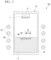
- FIG. 2 is a schematic cross-sectional view of the single crystal growth apparatus 101 according to the second embodiment.
- the apparatus 101 for growing a single crystal shown in FIG. 2 is different from the apparatus 100 for growing a single crystal shown in FIG. 1 in the structure of the deposition preventing member 14 .
- the other configurations are the same, and the description thereof is omitted.
- the deposition preventing member 14 illustrated in FIG. 2 is a member disposed on the raw material M after the raw material is provided in the inner bottom 11 .
- the deposition preventing member 14 covers the central area of the inner bottom 11 in a plan view from the crystal mounting part 12 .
- the deposition preventing member 14 covers the central area of the raw material M.
- the deposition preventing member 14 may cover a wider range than the central area.
- the first surface 14 a on the crystal mounting part 12 side of the deposition preventing member 14 shown in FIG. 2 is at the same height position as the raw material surface Ma of the raw material M.
- the first surface 14 a does not necessarily have to be at the same height position as the raw material surface Ma, and is preferably in a range within 20 mm from the raw material surface Ma. Alternatively, it is preferable that the first surface 14 a be in a range within 20% of the height of the distance from the raw material surface Ma to the surface of the seed crystal 1 .
- the deposition preventing member 14 shown in FIG. 2 includes a base 14 A and a surface layer 14 B.
- the surface layer 14 B covers at least the surface of the base 14 A on the side of the crystal mounting part 12 .
- the base 14 A is not particularly limited as long as it has heat resistance to the single crystal growth temperature.
- graphite or the like can be used.
- the surface layer 14 B may be made of metal carbide.
- the surface layer 14 B may be a coating film formed on the surface of the base 14 A, or may be a metal carbide powder mounted on the surface of the base 14 A.
- the same metal carbide as that of the first embodiment can be used.
- the surface layer 14 B is provided, at least the first surface 14 a on the crystal mounting part 12 side of the deposition preventing member 14 is made of metal carbide.
- the depositions are not deposited. Therefore, if the first surface 14 a is made of metal carbide, recrystallization of the source gas subjected to sublimation on the deposition preventing member 14 can be suppressed. That is, the apparatus 101 for growing the single crystal according to the second embodiment suppresses the generation of depositions, and suppresses the generation of different polytypes in the single crystal to be grown.
- FIG. 3 is a schematic cross-sectional view of the single crystal growth apparatus 102 according to the third embodiment.
- the single crystal growth apparatus 102 shown in FIG. 3 is different from the apparatus 100 for growing a single crystal shown in FIG. 1 in the structure of the deposition preventing member 15 .
- the other configurations are the same, and the description thereof is omitted.
- the deposition preventing member 15 shown in FIG. 3 is a member mounted on the raw material M after the raw material is provided in the inner bottom 11 .
- the deposition preventing member 15 covers the central area of the inner bottom 11 in a plan view from the crystal mounting part 12 .
- the deposition preventing member 15 covers the central area of the raw material M.
- the deposition preventing member 15 may cover a wider range than the central area.
- the first surface 15 a on the crystal mounting part 12 side of the deposition preventing member 15 shown in FIG. 3 is at the same height position as the raw material surface Ma of the raw material M.
- the first surface 15 a does not necessarily have to be at the same height position as the raw material surface Ma, and is preferably in a range within 20 mm from the raw material surface Ma. Alternatively, it is preferable that the first surface 15 a be in a range within 20% of the height of the distance from the raw material surface Ma to the surface of the seed crystal 1 .
- the deposition preventing member 15 shown in FIG. 3 includes a base 15 A and a surface layer 15 B.
- the surface layer 15 B covers at least the surface of the substrate 15 A on the side of the crystal mounting part 12 .
- the deposition preventing member 15 differs from the deposition preventing member 14 shown in FIG. 2 only in the shapes of the base materials 14 A and 15 A. Since the first surface 15 a is made of metal carbide, recrystallization of the source gas subjected to sublimation on the deposition preventing member 15 can be suppressed.
- the lower surface 15 Ab on the inner bottom 11 side of the base 15 A is in the shape of a cone whose diameter decreases toward the inner bottom 11 .
- the lower surface 15 Ab is an inclined surface which spreads toward the outer peripheral area, the source gas sublimated from the source M located below the deposition preventing member 15 can be guided to the outside of the crucible 10 where the source M is exposed. By preventing the stagnation of the raw material gas subjected to sublimation, it is possible to suppress recrystallization of the raw material at a position below the deposition preventing member 15 .
- FIG. 4 is a schematic cross-sectional view of a single crystal growth apparatus 103 according to the fourth embodiment.
- the apparatus 103 for growing a single crystal shown in FIG. 4 is different from the single crystal growth apparatus 100 shown in FIG. 1 in the structure of the deposition preventing member 16 .
- the other configurations are the same, and the description thereof is omitted.
- the deposition preventing member 16 illustrated in FIG. 4 is a member disposed on the raw material M after the raw material is provided in the inner bottom 11 .
- the deposition preventing member 16 covers the central area of the inner bottom 11 in a plan view from the crystal mounting part 12 , When the raw material M is provided in the inner bottom 11 , the deposition preventing member 16 covers the central area of the raw material M.
- the deposition preventing member 16 may cover a wider range than the central area.
- the deposition preventing member 16 shown in FIG. 4 includes a base 16 A, a surface layer 16 B, and a support 16 C.
- the surface layer 16 B covers at least the surface of the base 16 A on the side of the crystal mounting part 12 .
- the deposition preventing member 16 is different from the deposition preventing member 14 shown in FIG. 2 in that the deposition preventing member 16 includes the support 16 C. Since the first surface 16 a of the deposition preventing member 16 is made of metal carbide, it is possible to suppress recrystallization of the source gas subjected to sublimation on the deposition preventing member 16 .
- the support 16 C is provided on a second surface 16 b opposed to the first surface 16 a of the deposition preventing member 16 .
- the support 16 C separates the raw material surface Ma from the second surface 16 b .
- the first surface 16 a at the side of the crystal mounting part 12 of the deposition preventing member 16 exist in the area within 20 min from the raw material surface Ma.
- the space between the raw material surface Ma and the second surface 16 b is wide, a part of the raw material gas subjected to sublimation may enter this space, which may cause a deposition in the central area of the crucible 10 . Therefore, the distance between the second surface 16 b and the raw material surface Ma is preferably within 15 mm.
- FIG. 5 is a schematic cross-sectional view of the single crystal growth apparatus 104 according to the fifth embodiment.
- the single crystal growth apparatus 104 shown in FIG. 5 is different from the single crystal growth apparatus 100 shown in FIG. 1 in the structure of the deposition preventing member 17 .
- the other configurations are the same, and the description thereof is omitted.
- the deposition preventing member 17 shown in FIG. 5 is connected to the inner bottom 11 .
- the deposition preventing member 17 may be integrated with the inner bottom 11 .
- the deposition preventing member 17 overlaps the central area of the inner bottom 11 in a plan view from the crystal mounting part 12 .
- the deposition preventing member 17 may overlap with a wider range than the central area.
- the deposition preventing member 17 shown in FIG. 5 includes a support 17 A and a surface layer 17 B.
- the surface layer 17 B covers at least the surface of the support 17 A on the crystal mounting part 12 side.
- the deposition preventing member 17 differs from the deposition preventing member 14 shown in FIG. 2 in that the support 17 A is connected to the inner bottom 11 . Since the first surface 17 a of the deposition preventing member 17 is made of metal carbide, it is possible to suppress the source gas subjected to sublimation from being recrystallized on the deposition preventing member 17 .
- the first surface 17 a on the crystal mounting part 12 side of the deposition preventing member 17 shown in FIG. 5 is at the same height position as the raw material surface Ma of the raw material M.
- the first surface 17 a does not necessarily have to be at the same height position as the raw material surface Ma, and is preferably in a range within 20 mm from the raw material surface Ma.
- the raw material M is provided between the deposition preventing member 17 and the inner surface of the crucible 10 .
- the raw materials located below the deposition preventing members 13 , 14 , 15 and 16 shown in FIGS. 1 to 4 are inhibited from sublimation by the deposition preventing members 13 , 14 , 15 and 16 .
- the raw material M is not provided in the portion for which it is difficult to be sublimated, and the raw material M can be saved.
- the single crystal growth method according to the sixth embodiment is a single crystal growth method using the devices 100 , 101 , 102 , and 103 for growing a single crystal according to the first to fourth embodiments.
- the single crystal growth method according to the sixth embodiment includes, in the following order, a step of providing the raw material M in the inner bottom 11 ; a step of covering at least the surface on the crystal mounting part 12 side with the deposition preventing members 13 , 14 , 15 and 16 containing metal carbide in the central area of the diameter of the raw material surface Ma of the raw material NI in a plan view from the crystal mounting part 12 ; then, growing the single crystal placed on the crystal mounting part 12 by sublimating the raw material M by heating the raw material M.
- the raw material M is provided in the inner bottom 11 in the providing step.
- a powder raw material of SiC is filled in the inner bottom 11 .
- the raw material surface Ma of the raw material M be leveled in order to enhance the symmetry with respect to the crystal mounting part 12 .
- the deposition preventing members 13 , 14 , 15 and 16 are placed on the raw material M.
- the deposition preventing members 13 , 14 , 15 and 16 are provided so as to cover the central area.
- the deposition preventing members 13 , 14 , 15 and 16 may be provided to cover an area of 50% or more, or 80% or more of the inner diameter of the crucible 10 from the center at the position of the surface Ma of the raw material M. Further, it is desirable that the deposition preventing members 13 , 14 , 15 and 16 cover an area of which the temperature is at least 15° C. lower than the maximum temperature in the surface of the raw material.
- the first surfaces 13 a , 14 a , 15 a , 16 a on the crystal mounting part 12 side of the deposition preventing members 13 , 14 , 15 and 16 be placed within a range of 20 mm or less from the raw material surface Ma.
- the seed crystal 1 is placed in the crystal mounting part 12 at a position facing the raw material M. Mounting the seed crystal 1 may be performed before or after the raw material M is provided. After providing the seed crystal 1 and the raw material M, the crucible 10 is sealed.
- a current is supplied to the heating device 30 .
- the heating device 30 generates heat, and thermal radiation from the heating device 30 heats the container 10 .
- the raw material NI heated by the container 10 is sublimated and recrystallized on the surface of the seed crystal 1 so that the seed crystal 1 is grown.
- the temperature of the central area of the container 10 is lower than the peripheral area. A portion of the sublimated source gas is likely to be recrystallized in the central area of the container 10 .
- the deposition preventing members 13 , 14 , 15 and 16 in the central area of the raw material M, the raw material particles used as the starting point of recrystallization are prevented from being exposed to the raw material gas.
- the first surfaces 13 a , 14 a , 15 a , 16 a of the deposition preventing members 13 , 14 , 15 and 16 are made of metal carbide and it is difficult for them to adsorb SiC.
- the source gas subjected to sublimation is suppressed from being recrystallized to become a deposition on the deposition preventing members 13 , 14 , 15 and 16 .
- the generation of deposition it is possible to suppress the generation of different polytypes in the crystal-growing single crystal.
- the present invention is not limited to this embodiment, and within the scope of the subject matter of the present invention described in the claims, various modifications and changes are possible.
- the respective configurations of the single crystal growth crucible according to the first to fifth embodiments may be combined, and the single crystal growth crucible according to the first to fifth embodiments and the single crystal growth method according to the sixth embodiment may be combined.
- a crystal growth crucible in which a cylindrical internal space was provided was prepared. Then, the inner bottom of the crystal growth crucible was filled with the SiC powder as a raw material. Next, the deposition preventing member 16 (see FIG. 4 ) according to the fourth embodiment was placed on the filled SiC powder raw material.
- the base 16 A and the support 16 C are made of graphite, and the surface layer 16 B is made of tantalum carbide which covers the surface of the base 16 A.
- the distance between the first surface 16 a of the deposition preventing member 16 and the material surface Ma was 10 mm, and a space of 5 mm in height was formed between the second surface 16 b and the material surface Ma.
- FIG. 6 is a photograph of the surface of the deposition preventing member 16 after growing a single crystal under the conditions of Example 1. As shown in FIG. 6 , no deposition was observed on the deposition preventing member 16 .
- Comparative Example 1 differs from Example 1 in that the deposition preventing member 16 was not used. That is, the crystal growth of the SiC ingot was carried out without covering the raw material surface. The other conditions were the same as in Example 1 to carry out the crystal growth of the single crystal.
- FIG. 7 is a photograph of the surface of the raw material after growing the single crystal under the conditions of Comparative Example 1. As shown in FIG. 7 , many depositions were confirmed on the surface of the raw material.
- FIG. 8 is a cross-sectional photograph of the vicinity of the surface of the raw material in the central area after depositing the single crystal under the conditions of Comparative Example 1. As shown in FIG. 8 , it can be confirmed that recrystallization of the raw material occurs in the central area of the raw material.
- Comparative Example 2 differs from Example 1 in that the surface layer 16 B of the deposition preventing member 16 was not provided. That is, in Comparative Example 2, the deposition preventing member made of graphite was mounted in the central area of the raw material. The other conditions were the same as in Example 1 to carry out the crystal growth of the single crystal.
- FIG. 9 is a photograph of the raw material surface after growing the single crystal under the conditions of Comparative Example 2. As shown in FIG. 9 , the deposition was confirmed on the surface of the raw material, That is, in the case of graphite or the like that reacts with SiC, the effect of suppressing the depositions sufficiently cannot be obtained.
Landscapes
- Chemical & Material Sciences (AREA)
- Engineering & Computer Science (AREA)
- Crystallography & Structural Chemistry (AREA)
- Materials Engineering (AREA)
- Metallurgy (AREA)
- Organic Chemistry (AREA)
- Inorganic Chemistry (AREA)
- Crystals, And After-Treatments Of Crystals (AREA)
Abstract
Description
- [Patent Document 1] Japanese Unexamined Patent Application, First Publication No. 2010-275166
-
- (1) A single crystal growth crucible according to the first aspect comprises an inner bottom,
- a crystal mounting part, and
- a deposition preventing member,
- wherein a raw material is provided in the inner bottom,
- the crystal mounting part faces the inner bottom,
- the deposition preventing member has a first surface comprising metal carbide,
- the first surface is disposed to face the crystal mounting part,
- the deposition preventing member is disposed in a central area of the inner bottom in a plan view from the crystal mounting part,
- the central area has a similar shape as a cross section of the inner bottom at a position of the surface of the raw material in a plan view from the crystal mounting part, and the central area is an area of 20 area % of a cross sectional area of the cross section from a center,
- (2) In the single crystal growth crucible according to the above aspect, the first surface on the crystal mounting part side of the deposition preventing member is in a range within 20 mm from the surface of the raw material provided in the inner bottom.
- (3) In the single crystal growth crucible according to the above aspect, the deposition preventing member is a member mounted on the raw material after the raw material is provided in the inner bottom.
- (4) In the single crystal growth crucible according to the above aspect, the deposition preventing member comprises a support on a second surface opposite to the first surface on the crystal mounting part side, and
- the support separates the surface of the raw material which is provided in the inner bottom from the second surface.
- (5) in the single crystal growth crucible according to the above aspect, the deposition preventing member is connected to the inner bottom.
- (6) In the single crystal growth crucible according to the above aspect, a surface of the deposition preventing member on the crystal mounting part side is covered with metal carbide.
- (7) In the single crystal growth crucible according to the above aspect, the deposition preventing member is made of metal carbide.
- (8) In the single crystal growth crucible according to the above aspect, the metal carbide is tantalum carbide.
- (9) in the single crystal growth method according to the second aspect, in a single crystal growth crucible comprising an inner bottom for providing a raw material, and a crystal mounting part facing the inner bottom, the method comprises in the following order:
- providing the raw material in the inner bottom;
- covering a central area of the surface of the raw material with a deposition preventing member containing metal carbide on at least a surface on the side of the crystal mounting part in a plan view from the crystal mounting part; and
- growing a single crystal disposed in the crystal mounting part by sublimating the raw material by heating,
- wherein the central area is similar to a shape of a cross section of the inner bottom at a position of the surface of the raw material in a plan view from the crystal mounting part, and the central area is an area of 20 area % of a cross section area of the cross section from a center.
- (10) In the covering step of the single crystal growth method according to the above aspect, a first surface on the crystal mounting part side of the deposition preventing member is mounted in a range within 20 mm from the surface of the raw material provided in the inner bottom.
- (11) In the covering step of the single crystal growth apparatus according to the above aspect, a second surface of the deposition preventing member opposite to the first surface on the crystal mounting part is arranged to provide a space between the second surface and the surface of the raw material provided in the inner bottom.
- (12) in the single crystal growth method according to the third aspect, in a single crystal growth crucible comprising an inner bottom for providing a raw material, and a crystal mounting part facing the inner bottom,
- the method comprises in the following order:
- providing the raw material in the inner bottom,
- covering at least a surface on the side of the crystal mounting part with a deposition preventing member comprising metal carbide in an area of which the temperature is at least 15° C. lower than a maximum temperature of the surface of the raw material in a plan view from the crystal mounting part, and
- growing a single crystal disposed in the crystal mounting part by sublimating the raw material by heating.
-
- 1: Seed crystal
- 10: Container
- 11: Inner bottom
- 12: Crystal mounting part
- 13, 14, 15, 16, 17: Deposition preventing member
- 14A, 15A, 16A: Base
- 17A: Support
- 14B, 15B, 16B, 17B: Surface layer
- 16C: Support
- 13 a, 14 a, 15 a, 16 a, 17 a: First surface
- 14 b, 16 b: Second surface
- 15Ab: Lower surface
- 30: Heating device
- 100, 101, 102, 103: Single crystal growth apparatus
- M: Raw material
- Ma: Raw material surface
Claims (7)
Applications Claiming Priority (2)
| Application Number | Priority Date | Filing Date | Title |
|---|---|---|---|
| JP2018-167062 | 2018-09-06 | ||
| JP2018167062A JP7170470B2 (en) | 2018-09-06 | 2018-09-06 | Single crystal growth crucible and single crystal growth method |
Publications (2)
| Publication Number | Publication Date |
|---|---|
| US20200080233A1 US20200080233A1 (en) | 2020-03-12 |
| US11814749B2 true US11814749B2 (en) | 2023-11-14 |
Family
ID=69718998
Family Applications (1)
| Application Number | Title | Priority Date | Filing Date |
|---|---|---|---|
| US16/559,863 Active 2039-11-01 US11814749B2 (en) | 2018-09-06 | 2019-09-04 | Single crystal growth crucible and single crystal growth method |
Country Status (3)
| Country | Link |
|---|---|
| US (1) | US11814749B2 (en) |
| JP (1) | JP7170470B2 (en) |
| CN (1) | CN110878422B (en) |
Families Citing this family (2)
| Publication number | Priority date | Publication date | Assignee | Title |
|---|---|---|---|---|
| JP7166111B2 (en) * | 2018-09-06 | 2022-11-07 | 昭和電工株式会社 | Single crystal growth method |
| CN113622016B (en) * | 2021-08-17 | 2022-04-19 | 福建北电新材料科技有限公司 | Silicon carbide crystal growth apparatus and crystal growth method |
Citations (18)
| Publication number | Priority date | Publication date | Assignee | Title |
|---|---|---|---|---|
| JPH061698A (en) | 1992-06-19 | 1994-01-11 | Sharp Corp | Method for producing bulk silicon carbide single crystal |
| JPH08295595A (en) * | 1995-04-21 | 1996-11-12 | Toyota Central Res & Dev Lab Inc | Single crystal growth equipment |
| JPH11268990A (en) | 1998-03-20 | 1999-10-05 | Denso Corp | Method and apparatus for producing single crystal |
| JP2000264795A (en) * | 1999-03-23 | 2000-09-26 | Denso Corp | Apparatus for producing silicon carbide single crystal and method for producing silicon carbide single crystal |
| US20010004877A1 (en) | 1999-12-27 | 2001-06-28 | Masashi Shigeto | Method and apparatus for producing silicon carbide single crystal |
| CN1554808A (en) | 2003-12-24 | 2004-12-15 | 山东大学 | A device and method for growing a large-diameter 6H-SiC single crystal with semiconductor properties |
| JP2006069851A (en) * | 2004-09-02 | 2006-03-16 | Bridgestone Corp | Method and device for manufacturing silicon carbide single crystal |
| JP2009091173A (en) | 2007-10-04 | 2009-04-30 | Denso Corp | Silicon carbide single crystal manufacturing equipment |
| JP2010275166A (en) | 2009-06-01 | 2010-12-09 | Mitsubishi Electric Corp | Method for producing silicon carbide single crystal |
| JP2011178590A (en) * | 2010-02-26 | 2011-09-15 | Showa Denko Kk | Component-adjustment member and single crystal growth device provided therewith |
| JP2012020893A (en) * | 2010-07-13 | 2012-02-02 | Denso Corp | Apparatus for manufacturing silicon carbide single crystal, and method for manufacturing silicon carbide single crystal |
| CN104246023A (en) | 2012-04-20 | 2014-12-24 | 贰陆股份公司 | LARGE DIAMETER, HIGH QUALITY SiC SINGLE CRYSTALS, METHOD AND APPARATUS |
| TW201504488A (en) | 2013-07-31 | 2015-02-01 | 太平洋水泥股份有限公司 | Silicon carbide powder and method for producing silicon carbide single crystal |
| JP2015212207A (en) | 2014-05-02 | 2015-11-26 | 新日鐵住金株式会社 | Method for manufacturing silicon carbide single crystal ingot |
| CN105734671A (en) | 2014-12-10 | 2016-07-06 | 北京天科合达半导体股份有限公司 | High-quality silicon carbide crystal growth method |
| CN207498521U (en) | 2017-11-02 | 2018-06-15 | 福建北电新材料科技有限公司 | A kind of silicon carbide monocrystal growth device for promoting quality |
| WO2019171901A1 (en) | 2018-03-08 | 2019-09-12 | 信越半導体株式会社 | Production method for silicon carbide single crystal |
| US20200080229A1 (en) | 2018-09-06 | 2020-03-12 | Showa Denko K.K. | Single crystal growth method |
-
2018
- 2018-09-06 JP JP2018167062A patent/JP7170470B2/en active Active
-
2019
- 2019-08-21 CN CN201910772738.2A patent/CN110878422B/en active Active
- 2019-09-04 US US16/559,863 patent/US11814749B2/en active Active
Patent Citations (18)
| Publication number | Priority date | Publication date | Assignee | Title |
|---|---|---|---|---|
| JPH061698A (en) | 1992-06-19 | 1994-01-11 | Sharp Corp | Method for producing bulk silicon carbide single crystal |
| JPH08295595A (en) * | 1995-04-21 | 1996-11-12 | Toyota Central Res & Dev Lab Inc | Single crystal growth equipment |
| JPH11268990A (en) | 1998-03-20 | 1999-10-05 | Denso Corp | Method and apparatus for producing single crystal |
| JP2000264795A (en) * | 1999-03-23 | 2000-09-26 | Denso Corp | Apparatus for producing silicon carbide single crystal and method for producing silicon carbide single crystal |
| US20010004877A1 (en) | 1999-12-27 | 2001-06-28 | Masashi Shigeto | Method and apparatus for producing silicon carbide single crystal |
| CN1554808A (en) | 2003-12-24 | 2004-12-15 | 山东大学 | A device and method for growing a large-diameter 6H-SiC single crystal with semiconductor properties |
| JP2006069851A (en) * | 2004-09-02 | 2006-03-16 | Bridgestone Corp | Method and device for manufacturing silicon carbide single crystal |
| JP2009091173A (en) | 2007-10-04 | 2009-04-30 | Denso Corp | Silicon carbide single crystal manufacturing equipment |
| JP2010275166A (en) | 2009-06-01 | 2010-12-09 | Mitsubishi Electric Corp | Method for producing silicon carbide single crystal |
| JP2011178590A (en) * | 2010-02-26 | 2011-09-15 | Showa Denko Kk | Component-adjustment member and single crystal growth device provided therewith |
| JP2012020893A (en) * | 2010-07-13 | 2012-02-02 | Denso Corp | Apparatus for manufacturing silicon carbide single crystal, and method for manufacturing silicon carbide single crystal |
| CN104246023A (en) | 2012-04-20 | 2014-12-24 | 贰陆股份公司 | LARGE DIAMETER, HIGH QUALITY SiC SINGLE CRYSTALS, METHOD AND APPARATUS |
| TW201504488A (en) | 2013-07-31 | 2015-02-01 | 太平洋水泥股份有限公司 | Silicon carbide powder and method for producing silicon carbide single crystal |
| JP2015212207A (en) | 2014-05-02 | 2015-11-26 | 新日鐵住金株式会社 | Method for manufacturing silicon carbide single crystal ingot |
| CN105734671A (en) | 2014-12-10 | 2016-07-06 | 北京天科合达半导体股份有限公司 | High-quality silicon carbide crystal growth method |
| CN207498521U (en) | 2017-11-02 | 2018-06-15 | 福建北电新材料科技有限公司 | A kind of silicon carbide monocrystal growth device for promoting quality |
| WO2019171901A1 (en) | 2018-03-08 | 2019-09-12 | 信越半導体株式会社 | Production method for silicon carbide single crystal |
| US20200080229A1 (en) | 2018-09-06 | 2020-03-12 | Showa Denko K.K. | Single crystal growth method |
Non-Patent Citations (5)
| Title |
|---|
| A. Pisch, et al. publication entitled "Evaporation behavior of SiC powder for single crystal growth—an experimental study on thermodynamics and kinetics," Materials Science Forum, vol. 338-342, pp. 91-94 (2000) (1 page total). |
| Communication dated Jan. 7, 2021, from the China National Intellectual Property Administration in application No. 201910772738.2. |
| Non-Final Office Action dated Feb. 8, 2021 in related U.S. Appl. No. 16/559,875. |
| Office Action dated Dec. 30, 2020 from the China National Intellectual Property Administration in related Chinese Application No. 201910751559.0. |
| Office Action dated May 17, 2022 in Japanese Application No. 2018-167062. |
Also Published As
| Publication number | Publication date |
|---|---|
| JP7170470B2 (en) | 2022-11-14 |
| CN110878422B (en) | 2021-09-24 |
| US20200080233A1 (en) | 2020-03-12 |
| JP2020040842A (en) | 2020-03-19 |
| CN110878422A (en) | 2020-03-13 |
Similar Documents
| Publication | Publication Date | Title |
|---|---|---|
| US12460314B2 (en) | Silicon carbide substrate and method of growing SiC single crystal boules | |
| JP5562641B2 (en) | Micropipe-free silicon carbide and method for producing the same | |
| JP4121555B2 (en) | Apparatus and method for epitaxial growth of objects by CVD | |
| CN102400224B (en) | Silicon carbide single crystal and manufacturing method of the same | |
| US11111599B2 (en) | Single crystal growth method which includes covering a part of a surface of a raw material for sublimation with a metal carbide powder | |
| CN110325670B (en) | Silicon carbide substrate and method for growing SiC single crystal ingot | |
| JP2002060297A (en) | Apparatus and method for growing single crystal | |
| JPWO2017188381A1 (en) | Vapor phase epitaxial growth method and manufacturing method of substrate with epitaxial layer | |
| JP7258273B2 (en) | SiC single crystal manufacturing method and coated member | |
| JP2013212952A (en) | Method for manufacturing silicon carbide single crystal | |
| US11814749B2 (en) | Single crystal growth crucible and single crystal growth method | |
| JP7305818B1 (en) | Thermal field adjustment method for silicon carbide single crystal growth | |
| WO2013031154A1 (en) | Semiconductor wafer manufacturing method, and semiconductor wafer | |
| JP2024508945A (en) | How to grow high quality single crystal silicon carbide | |
| JP2017119594A (en) | Method for producing single crystal SiC and container | |
| US20210172085A1 (en) | SiC SUBSTRATE AND SiC SINGLE CRYSTAL MANUFACTURING METHOD | |
| JP5397503B2 (en) | Single crystal growth equipment | |
| EP4206366A1 (en) | Sic polycrystal manufacturing method | |
| JP2006124247A (en) | Silicon carbide single crystal and silicon carbide substrate | |
| JP2015067499A (en) | Single crystal manufacturing apparatus and single crystal manufacturing method |
Legal Events
| Date | Code | Title | Description |
|---|---|---|---|
| FEPP | Fee payment procedure |
Free format text: ENTITY STATUS SET TO UNDISCOUNTED (ORIGINAL EVENT CODE: BIG.); ENTITY STATUS OF PATENT OWNER: LARGE ENTITY |
|
| AS | Assignment |
Owner name: SHOWA DENKO K.K., JAPAN Free format text: ASSIGNMENT OF ASSIGNORS INTEREST;ASSIGNOR:FUJIKAWA, YOHEI;REEL/FRAME:050277/0436 Effective date: 20190830 |
|
| STPP | Information on status: patent application and granting procedure in general |
Free format text: NON FINAL ACTION MAILED |
|
| STPP | Information on status: patent application and granting procedure in general |
Free format text: RESPONSE TO NON-FINAL OFFICE ACTION ENTERED AND FORWARDED TO EXAMINER |
|
| STPP | Information on status: patent application and granting procedure in general |
Free format text: FINAL REJECTION MAILED |
|
| STPP | Information on status: patent application and granting procedure in general |
Free format text: ADVISORY ACTION MAILED |
|
| STPP | Information on status: patent application and granting procedure in general |
Free format text: DOCKETED NEW CASE - READY FOR EXAMINATION |
|
| STPP | Information on status: patent application and granting procedure in general |
Free format text: NON FINAL ACTION MAILED |
|
| STPP | Information on status: patent application and granting procedure in general |
Free format text: RESPONSE TO NON-FINAL OFFICE ACTION ENTERED AND FORWARDED TO EXAMINER |
|
| STPP | Information on status: patent application and granting procedure in general |
Free format text: RESPONSE TO NON-FINAL OFFICE ACTION ENTERED AND FORWARDED TO EXAMINER |
|
| STPP | Information on status: patent application and granting procedure in general |
Free format text: FINAL REJECTION MAILED |
|
| STPP | Information on status: patent application and granting procedure in general |
Free format text: NON FINAL ACTION MAILED |
|
| AS | Assignment |
Owner name: RESONAC CORPORATION, JAPAN Free format text: CHANGE OF NAME;ASSIGNOR:SHOWA DENKO K.K.;REEL/FRAME:064082/0513 Effective date: 20230623 |
|
| STPP | Information on status: patent application and granting procedure in general |
Free format text: RESPONSE TO NON-FINAL OFFICE ACTION ENTERED AND FORWARDED TO EXAMINER |
|
| STPP | Information on status: patent application and granting procedure in general |
Free format text: NOTICE OF ALLOWANCE MAILED -- APPLICATION RECEIVED IN OFFICE OF PUBLICATIONS |
|
| STPP | Information on status: patent application and granting procedure in general |
Free format text: PUBLICATIONS -- ISSUE FEE PAYMENT RECEIVED |
|
| STPP | Information on status: patent application and granting procedure in general |
Free format text: PUBLICATIONS -- ISSUE FEE PAYMENT VERIFIED |
|
| STCF | Information on status: patent grant |
Free format text: PATENTED CASE |
|
| AS | Assignment |
Owner name: RESONAC CORPORATION, JAPAN Free format text: CHANGE OF ADDRESS;ASSIGNOR:RESONAC CORPORATION;REEL/FRAME:066599/0037 Effective date: 20231001 |