US11776974B2 - Photoelectric conversion apparatus, photoelectric conversion system, and moving body - Google Patents
Photoelectric conversion apparatus, photoelectric conversion system, and moving body Download PDFInfo
- Publication number
- US11776974B2 US11776974B2 US16/912,394 US202016912394A US11776974B2 US 11776974 B2 US11776974 B2 US 11776974B2 US 202016912394 A US202016912394 A US 202016912394A US 11776974 B2 US11776974 B2 US 11776974B2
- Authority
- US
- United States
- Prior art keywords
- photoelectric conversion
- transfer transistor
- transistor
- conversion apparatus
- input node
- Prior art date
- Legal status (The legal status is an assumption and is not a legal conclusion. Google has not performed a legal analysis and makes no representation as to the accuracy of the status listed.)
- Active, expires
Links
- 238000006243 chemical reaction Methods 0.000 title claims abstract description 227
- 238000012546 transfer Methods 0.000 claims abstract description 145
- 230000003321 amplification Effects 0.000 claims abstract description 39
- 238000003199 nucleic acid amplification method Methods 0.000 claims abstract description 39
- 239000004065 semiconductor Substances 0.000 claims description 53
- 238000012545 processing Methods 0.000 claims description 52
- 239000000758 substrate Substances 0.000 claims description 17
- 230000003287 optical effect Effects 0.000 claims description 16
- 238000000034 method Methods 0.000 claims description 15
- 238000009792 diffusion process Methods 0.000 claims description 3
- 230000008569 process Effects 0.000 claims description 3
- 238000010586 diagram Methods 0.000 description 23
- 238000001514 detection method Methods 0.000 description 14
- 230000006870 function Effects 0.000 description 14
- 230000005856 abnormality Effects 0.000 description 6
- 230000001276 controlling effect Effects 0.000 description 6
- 238000007781 pre-processing Methods 0.000 description 6
- 238000004364 calculation method Methods 0.000 description 5
- 230000000875 corresponding effect Effects 0.000 description 4
- 230000035945 sensitivity Effects 0.000 description 4
- 238000005036 potential barrier Methods 0.000 description 3
- 238000004891 communication Methods 0.000 description 2
- 238000012937 correction Methods 0.000 description 2
- 230000002596 correlated effect Effects 0.000 description 2
- 230000007547 defect Effects 0.000 description 2
- 238000005286 illumination Methods 0.000 description 2
- 238000005070 sampling Methods 0.000 description 2
- XUIMIQQOPSSXEZ-UHFFFAOYSA-N Silicon Chemical compound [Si] XUIMIQQOPSSXEZ-UHFFFAOYSA-N 0.000 description 1
- 238000009825 accumulation Methods 0.000 description 1
- 230000004888 barrier function Effects 0.000 description 1
- 230000008901 benefit Effects 0.000 description 1
- 230000005540 biological transmission Effects 0.000 description 1
- 230000008859 change Effects 0.000 description 1
- 230000006835 compression Effects 0.000 description 1
- 238000007906 compression Methods 0.000 description 1
- 239000000470 constituent Substances 0.000 description 1
- 238000011161 development Methods 0.000 description 1
- 230000000694 effects Effects 0.000 description 1
- 230000005669 field effect Effects 0.000 description 1
- 239000000463 material Substances 0.000 description 1
- 229910044991 metal oxide Inorganic materials 0.000 description 1
- 150000004706 metal oxides Chemical class 0.000 description 1
- 238000012986 modification Methods 0.000 description 1
- 230000004048 modification Effects 0.000 description 1
- 238000012544 monitoring process Methods 0.000 description 1
- 230000002265 prevention Effects 0.000 description 1
- 230000000717 retained effect Effects 0.000 description 1
- 230000002441 reversible effect Effects 0.000 description 1
- 229920006395 saturated elastomer Polymers 0.000 description 1
- 238000004904 shortening Methods 0.000 description 1
- 229910052710 silicon Inorganic materials 0.000 description 1
- 239000010703 silicon Substances 0.000 description 1
- 230000000087 stabilizing effect Effects 0.000 description 1
- 230000001360 synchronised effect Effects 0.000 description 1
Images


Classifications
-
- H—ELECTRICITY
- H10—SEMICONDUCTOR DEVICES; ELECTRIC SOLID-STATE DEVICES NOT OTHERWISE PROVIDED FOR
- H10F—INORGANIC SEMICONDUCTOR DEVICES SENSITIVE TO INFRARED RADIATION, LIGHT, ELECTROMAGNETIC RADIATION OF SHORTER WAVELENGTH OR CORPUSCULAR RADIATION
- H10F39/00—Integrated devices, or assemblies of multiple devices, comprising at least one element covered by group H10F30/00, e.g. radiation detectors comprising photodiode arrays
- H10F39/80—Constructional details of image sensors
- H10F39/813—Electronic components shared by multiple pixels, e.g. one amplifier shared by two pixels
-
- H01L27/14612—
-
- H—ELECTRICITY
- H10—SEMICONDUCTOR DEVICES; ELECTRIC SOLID-STATE DEVICES NOT OTHERWISE PROVIDED FOR
- H10F—INORGANIC SEMICONDUCTOR DEVICES SENSITIVE TO INFRARED RADIATION, LIGHT, ELECTROMAGNETIC RADIATION OF SHORTER WAVELENGTH OR CORPUSCULAR RADIATION
- H10F39/00—Integrated devices, or assemblies of multiple devices, comprising at least one element covered by group H10F30/00, e.g. radiation detectors comprising photodiode arrays
- H10F39/80—Constructional details of image sensors
- H10F39/803—Pixels having integrated switching, control, storage or amplification elements
- H10F39/8037—Pixels having integrated switching, control, storage or amplification elements the integrated elements comprising a transistor
-
- H01L27/14603—
-
- H01L27/14627—
-
- H01L27/14831—
-
- H—ELECTRICITY
- H04—ELECTRIC COMMUNICATION TECHNIQUE
- H04N—PICTORIAL COMMUNICATION, e.g. TELEVISION
- H04N25/00—Circuitry of solid-state image sensors [SSIS]; Control thereof
- H04N25/50—Control of the SSIS exposure
- H04N25/57—Control of the dynamic range
- H04N25/59—Control of the dynamic range by controlling the amount of charge storable in the pixel, e.g. modification of the charge conversion ratio of the floating node capacitance
-
- H—ELECTRICITY
- H04—ELECTRIC COMMUNICATION TECHNIQUE
- H04N—PICTORIAL COMMUNICATION, e.g. TELEVISION
- H04N25/00—Circuitry of solid-state image sensors [SSIS]; Control thereof
- H04N25/70—SSIS architectures; Circuits associated therewith
- H04N25/703—SSIS architectures incorporating pixels for producing signals other than image signals
- H04N25/704—Pixels specially adapted for focusing, e.g. phase difference pixel sets
-
- H—ELECTRICITY
- H04—ELECTRIC COMMUNICATION TECHNIQUE
- H04N—PICTORIAL COMMUNICATION, e.g. TELEVISION
- H04N25/00—Circuitry of solid-state image sensors [SSIS]; Control thereof
- H04N25/70—SSIS architectures; Circuits associated therewith
- H04N25/71—Charge-coupled device [CCD] sensors; Charge-transfer registers specially adapted for CCD sensors
- H04N25/745—Circuitry for generating timing or clock signals
-
- H—ELECTRICITY
- H04—ELECTRIC COMMUNICATION TECHNIQUE
- H04N—PICTORIAL COMMUNICATION, e.g. TELEVISION
- H04N25/00—Circuitry of solid-state image sensors [SSIS]; Control thereof
- H04N25/70—SSIS architectures; Circuits associated therewith
- H04N25/71—Charge-coupled device [CCD] sensors; Charge-transfer registers specially adapted for CCD sensors
- H04N25/75—Circuitry for providing, modifying or processing image signals from the pixel array
-
- H—ELECTRICITY
- H04—ELECTRIC COMMUNICATION TECHNIQUE
- H04N—PICTORIAL COMMUNICATION, e.g. TELEVISION
- H04N25/00—Circuitry of solid-state image sensors [SSIS]; Control thereof
- H04N25/70—SSIS architectures; Circuits associated therewith
- H04N25/76—Addressed sensors, e.g. MOS or CMOS sensors
- H04N25/77—Pixel circuitry, e.g. memories, A/D converters, pixel amplifiers, shared circuits or shared components
- H04N25/771—Pixel circuitry, e.g. memories, A/D converters, pixel amplifiers, shared circuits or shared components comprising storage means other than floating diffusion
-
- H—ELECTRICITY
- H04—ELECTRIC COMMUNICATION TECHNIQUE
- H04N—PICTORIAL COMMUNICATION, e.g. TELEVISION
- H04N25/00—Circuitry of solid-state image sensors [SSIS]; Control thereof
- H04N25/70—SSIS architectures; Circuits associated therewith
- H04N25/76—Addressed sensors, e.g. MOS or CMOS sensors
- H04N25/77—Pixel circuitry, e.g. memories, A/D converters, pixel amplifiers, shared circuits or shared components
- H04N25/778—Pixel circuitry, e.g. memories, A/D converters, pixel amplifiers, shared circuits or shared components comprising amplifiers shared between a plurality of pixels, i.e. at least one part of the amplifier must be on the sensor array itself
-
- H—ELECTRICITY
- H04—ELECTRIC COMMUNICATION TECHNIQUE
- H04N—PICTORIAL COMMUNICATION, e.g. TELEVISION
- H04N25/00—Circuitry of solid-state image sensors [SSIS]; Control thereof
- H04N25/70—SSIS architectures; Circuits associated therewith
- H04N25/76—Addressed sensors, e.g. MOS or CMOS sensors
- H04N25/7795—Circuitry for generating timing or clock signals
-
- H—ELECTRICITY
- H04—ELECTRIC COMMUNICATION TECHNIQUE
- H04N—PICTORIAL COMMUNICATION, e.g. TELEVISION
- H04N25/00—Circuitry of solid-state image sensors [SSIS]; Control thereof
- H04N25/70—SSIS architectures; Circuits associated therewith
- H04N25/76—Addressed sensors, e.g. MOS or CMOS sensors
- H04N25/78—Readout circuits for addressed sensors, e.g. output amplifiers or A/D converters
-
- H—ELECTRICITY
- H10—SEMICONDUCTOR DEVICES; ELECTRIC SOLID-STATE DEVICES NOT OTHERWISE PROVIDED FOR
- H10F—INORGANIC SEMICONDUCTOR DEVICES SENSITIVE TO INFRARED RADIATION, LIGHT, ELECTROMAGNETIC RADIATION OF SHORTER WAVELENGTH OR CORPUSCULAR RADIATION
- H10F39/00—Integrated devices, or assemblies of multiple devices, comprising at least one element covered by group H10F30/00, e.g. radiation detectors comprising photodiode arrays
- H10F39/10—Integrated devices
- H10F39/12—Image sensors
- H10F39/15—Charge-coupled device [CCD] image sensors
- H10F39/153—Two-dimensional or three-dimensional array CCD image sensors
-
- H—ELECTRICITY
- H10—SEMICONDUCTOR DEVICES; ELECTRIC SOLID-STATE DEVICES NOT OTHERWISE PROVIDED FOR
- H10F—INORGANIC SEMICONDUCTOR DEVICES SENSITIVE TO INFRARED RADIATION, LIGHT, ELECTROMAGNETIC RADIATION OF SHORTER WAVELENGTH OR CORPUSCULAR RADIATION
- H10F39/00—Integrated devices, or assemblies of multiple devices, comprising at least one element covered by group H10F30/00, e.g. radiation detectors comprising photodiode arrays
- H10F39/80—Constructional details of image sensors
- H10F39/802—Geometry or disposition of elements in pixels, e.g. address-lines or gate electrodes
-
- H—ELECTRICITY
- H10—SEMICONDUCTOR DEVICES; ELECTRIC SOLID-STATE DEVICES NOT OTHERWISE PROVIDED FOR
- H10F—INORGANIC SEMICONDUCTOR DEVICES SENSITIVE TO INFRARED RADIATION, LIGHT, ELECTROMAGNETIC RADIATION OF SHORTER WAVELENGTH OR CORPUSCULAR RADIATION
- H10F39/00—Integrated devices, or assemblies of multiple devices, comprising at least one element covered by group H10F30/00, e.g. radiation detectors comprising photodiode arrays
- H10F39/80—Constructional details of image sensors
- H10F39/805—Coatings
- H10F39/8053—Colour filters
-
- H—ELECTRICITY
- H10—SEMICONDUCTOR DEVICES; ELECTRIC SOLID-STATE DEVICES NOT OTHERWISE PROVIDED FOR
- H10F—INORGANIC SEMICONDUCTOR DEVICES SENSITIVE TO INFRARED RADIATION, LIGHT, ELECTROMAGNETIC RADIATION OF SHORTER WAVELENGTH OR CORPUSCULAR RADIATION
- H10F39/00—Integrated devices, or assemblies of multiple devices, comprising at least one element covered by group H10F30/00, e.g. radiation detectors comprising photodiode arrays
- H10F39/80—Constructional details of image sensors
- H10F39/806—Optical elements or arrangements associated with the image sensors
- H10F39/8063—Microlenses
Definitions
- the present disclosure relates to a photoelectric conversion apparatus, a photoelectric conversion system, and a moving body.
- United States Patent Application Publication No. 2008/173909 discusses a configuration of a photoelectric conversion apparatus which includes a transistor for increasing a capacity in order to expand a dynamic range thereof.
- a photoelectric conversion apparatus which includes a transistor for increasing a capacity in order to expand a dynamic range thereof.
- one end of the transistor for increasing a capacity is connected to an input node of an amplification transistor, and the other end thereof is connected to a reset transistor.
- One end of the reset transistor is connected to the transistor for increasing a capacity, and the other end thereof is supplied with a power source voltage (VDD).
- VDD power source voltage
- a photoelectric conversion apparatus includes a photoelectric conversion portion, an amplification transistor, a first transfer transistor, a second transfer transistor, and a reset transistor.
- the amplification transistor has an input node to which electric charges generated by the photoelectric conversion portion are input.
- the first transfer transistor is configured to control transfer of the electric charges received from the photoelectric conversion portion.
- the second transfer transistor is arranged between the first transfer transistor and the input node.
- the reset transistor is connected to the input node.
- a photoelectric conversion apparatus includes a first semiconductor region, a second semiconductor region, an amplification transistor, and a first transfer transistor.
- the first semiconductor region is of a first conductive-type where electric charge of a first polarity same as a polarity of signal charge is a majority carrier.
- the second semiconductor region is of the first conductive-type to which electric charges accumulated in the first semiconductor region is transferred.
- the amplification transistor has an input node formed by the second semiconductor region.
- the first transfer transistor includes the first semiconductor region and the second semiconductor region.
- the second semiconductor region forms a source or a drain of a reset transistor, and a gate of a second transfer transistor is arranged to overlap with the second semiconductor region in a planar view.
- FIG. 1 is a block diagram illustrating a photoelectric conversion apparatus according to a first exemplary embodiment.
- FIG. 2 is a diagram illustrating a circuit configuration of a pixel according to the first exemplary embodiment.
- FIGS. 3 A, 3 B, and 3 C are diagrams schematically illustrating cross-sectional views and a potential of the pixel according to the first exemplary embodiment.
- FIG. 4 is a plan view of pixels according to the first exemplary embodiment.
- FIGS. 5 A and 5 B are timing charts illustrating read-out processing according to the first exemplary embodiment.
- FIGS. 6 A to 6 H are schematic diagrams illustrating a potential in the read-out processing according to the first exemplary embodiment.
- FIG. 7 is a timing chart illustrating read-out processing according to a second exemplary embodiment.
- FIG. 8 is a plan view of pixels according to a third exemplary embodiment.
- FIG. 9 is a diagram illustrating a circuit configuration of a pixel according to the third exemplary embodiment.
- FIG. 10 is an exploded perspective diagram illustrating a photoelectric conversion apparatus according to a fourth exemplary embodiment.
- FIGS. 11 A and 11 B are plan views of pixels of the photoelectric conversion apparatus according to the fourth exemplary embodiment.
- FIG. 12 is a block diagram illustrating a photoelectric conversion system according to a fifth exemplary embodiment.
- FIGS. 13 A and 13 B are schematic diagrams respectively illustrating a photoelectric conversion system and a moving body according to a sixth exemplary embodiment.
- FIG. 14 is a flowchart illustrating processing of the photoelectric conversion system according to the sixth exemplary embodiment.
- An electron serves as a signal carrier (signal charge).
- An N-type semiconductor region is provided as a first conductive-type semiconductor region where a carrier of a first polarity is a majority carrier
- a P-type semiconductor region is provided as a second conductive-type semiconductor region where a carrier of a second polarity is a majority carrier.
- the below-described exemplary embodiments can be also implemented in a case where a positive hole serves as the signal carrier.
- the P-type semiconductor region is provided as the first conductive-type semiconductor region
- the N-type semiconductor region is provided as the second conductive-type semiconductor region.
- an N-type metal-oxide-semiconductor (MOS) transistor is used as a transistor that constitutes a pixel.
- a state where the transistor is on refers to a state where a high-level (H-level) control signal is input to the N-type MOS transistor, so that the N-type MOS transistor is brought into a conduction state.
- a state where the transistor is off refers to a state where a low-level (L-level) control signal is input to the N-type MOS transistor, so that the N-type MOS transistor is brought into a non-conduction state.
- a P-type MOS transistor may be used instead of the N-type MOS transistor.
- the configuration may be changed as appropriate, e.g., a potential opposite to a potential of the N-type MOS transistor is applied when a control signal is supplied to the P-type MOS transistor.
- a connection relationship between circuit elements is described.
- a configuration thereof can be changed as appropriate, e.g., another element, such as a switch and a buffer, may be placed therebetween.
- FIG. 1 is a block diagram illustrating a schematic configuration of a photoelectric conversion apparatus according to a first exemplary embodiment.
- the photoelectric conversion apparatus includes a unit cell which detects light and outputs a signal.
- the photoelectric conversion apparatus according to the present exemplary embodiment includes a pixel as a unit cell, and is capable of executing image capturing.
- a photoelectric conversion apparatus that is not configured to execute image capturing according to the present exemplary embodiment can also produce a technical effect.
- a range finding sensor and a photometric sensor are given as the examples of the photoelectric conversion apparatus not configured to execute image capturing.
- the range finding sensor is a sensor such as a time of flight (TOF) sensor, which is typically used for generating distance information indicating a distance to an object.
- the photometric sensor is a sensor typically used for detecting brightness of an object.
- TOF time of flight
- the photoelectric conversion apparatus in FIG. 1 includes a pixel array unit 101 , a vertical scanning circuit 102 , a reading circuit 103 , a horizontal scanning circuit 104 , an output circuit 105 , and a control circuit 106 .
- the pixel array unit 101 includes a plurality of pixels 107 arranged in a row direction and a column direction.
- a light-shielded optical black pixel or a dummy pixel which does not output a signal may be arranged in the pixel array unit 101 in addition to a pixel for detecting an image capturing signal.
- the vertical scanning circuit 102 supplies a control signal for switching between an on state (conduction state) and an off state (non-conduction state) of transistors within the pixels 107 .
- a control signal line 108 for supplying a control signal is arranged for each of pixel rows.
- the plurality of pixels 107 arranged in one pixel row is connected to one control signal line 108 .
- the vertical scanning circuit 102 supplies a control signal to the plurality of pixels 107 arranged in the pixel rows upon receipt of a signal from the control circuit 106 .
- the reading circuit 103 executes signal processing such as amplification processing and analog-to-digital (A/D) conversion processing with respect to pixel signals output to a vertical output line 208 .
- the reading circuit 103 executes correlated double sampling processing based on the signal output when the pixels 107 are reset and a signal output when photoelectric conversion is executed.
- the horizontal scanning circuit 104 supplies a control signal to the reading circuit 103 .
- the control signal supplied from the horizontal scanning circuit 104 causes a pixel signal processed by the reading circuit 103 to be transferred to the output circuit 105 .
- the output circuit 105 outputs the signal to a signal processing unit provided outside the photoelectric conversion apparatus.
- the control circuit 106 is a circuit, such as a timing generator, which controls each of the circuits.
- the control circuit 106 supplies control signals for controlling the operations and operation timings of the vertical scanning circuit 102 , the reading circuit 103 , the horizontal scanning circuit 104 , and the output circuit 105 .
- At least a part of the control signals supplied to the vertical scanning circuit 102 , the reading circuit 103 , the horizontal scanning circuit 104 , and the output circuit 105 may be supplied from the outside of the photoelectric conversion apparatus instead of being supplied from the control circuit 106 .
- FIG. 2 is a schematic circuit diagram relating to the pixels 107 of the photoelectric conversion apparatus according to the present exemplary embodiment.
- a configuration of one pixel 107 is illustrated, and the rest of the pixels 107 are omitted.
- the pixel 107 includes a photoelectric conversion portion 201 , a first transfer transistor 202 , a second transfer transistor 203 , an amplification transistor 206 , a floating diffusion (FD) portion 204 , a reset transistor 205 , and a selection transistor 207 .
- the FD portion 204 is an input node of the amplification transistor 206 .
- each of the transistors is configured of a metal-oxide semiconductor field-effect transistor (MOSFET), and includes a gate serving as a control electrode arranged between a drain and a source in a planar view.
- MOSFET metal-oxide semiconductor field-effect transistor
- the amplification transistor 206 outputs a signal based on the potential of the input node to the selection transistor 207 .
- one end of the amplification transistor 206 is connected to a power source voltage VDD.
- the amplification transistor 206 is provided as a part of a source follower circuit, and a gate of the amplification transistor 206 is the input node.
- the photoelectric conversion portion 201 and the input node are connected to each other via the first transfer transistor 202 and the second transfer transistor 203 .
- the first transfer transistor 202 controls the electric charges transferred from the photoelectric conversion portion 201 .
- the second transfer transistor 203 is connected to the first transfer transistor 202 , and the other end thereof is connected to the input node.
- the second transfer transistor 203 controls the electric charges transferred from the photoelectric conversion portion 201 , and also controls a capacity value of the input node.
- the selection transistor 207 selectively connects the amplification transistor 206 and the vertical output line 208 . Then, the selection transistor 207 outputs a signal from the amplification transistor 206 to the vertical output line 208 at a synchronized timing with that of the control signal output from the vertical scanning circuit 102 .
- the reset transistor 205 is connected to the input node, and can set (reset) the input node to a reset potential.
- FIG. 3 A is a schematic cross-sectional diagram illustrating the photoelectric conversion portion 201 , the first transfer transistor 202 , and the second transfer transistor 203 .
- FIG. 3 B is a schematic diagram of the potential when the first transfer transistor 202 and the second transfer transistor 203 are off.
- FIG. 3 C is a schematic diagram of the potential when the first transfer transistor 202 is off and the second transfer transistor 203 is on.
- an N-type semiconductor region (first semiconductor region) which constitutes the photoelectric conversion portion 201 , an N-type semiconductor region (second semiconductor region) 210 which constitutes a part of the FD portion 204 , and an N-type semiconductor region 211 are arranged on a semiconductor substrate.
- the N-type semiconductor region 210 is formed between the gate of the second transfer transistor 203 and the gate of the reset transistor 205 in a planar view, and constitutes a part of the FD portion 204 .
- the N-type semiconductor region 211 is formed between the gate of the first transfer transistor 202 and the gate of the second transfer transistor 203 in a planar view.
- a capacity value of the FD portion 204 when the second transfer transistor 203 is turned on is greater than a capacity value thereof when the second transfer transistor 203 is turned off.
- the second transfer transistor 203 is turned on, a channel is formed under the gate of the second transfer transistor 203 .
- the N-type semiconductor region 211 is, thus, electrically connected to the N-type semiconductor region 210 , so that a capacity value of the FD portion 204 is increased. Accordingly, if the second transfer transistor 203 remains in the on state when the electric charges are transferred to the FD portion 204 from the photoelectric conversion portion 201 , the amount of electric charge that can be held at the PD portion 204 is increased.
- the capacity value of the FD portion 204 is increased. Accordingly, a voltage of the pixel signal output from the amplification transistor 206 is reduced, so that a dynamic range can be expanded. Meanwhile, if the second transfer transistor 203 remains in the off state when the electric charges are transferred to the FD portion 204 from the photoelectric conversion portion 201 , the capacity of the FD portion 204 is not increased. In other words, the capacity value of the PD portion 204 is not changed from its own capacity value. Accordingly, the amount of electric charge which can be held at the FD portion 204 is small. In other words, the capacity value of the FD portion 204 is small. Therefore, a voltage of the pixel signal output from the amplification transistor 206 is increased.
- a voltage change amount (electric charge voltage conversion efficiency) of the FD portion 204 with respect to one electric charge can be increased.
- a high electric charge voltage conversion efficiency can mean a high sensitivity. Therefore, by controlling the on/off state of the second transfer transistor 203 , the capacity value of the PD portion 204 can be changed, and the sensitivity thereof can be switched.
- the capacity of the FD portion 204 is smaller than the capacity of the photoelectric conversion portion 201 .
- the capacity of the FD portion 204 can be increased by the second transfer transistor 203 . Therefore, the dynamic range can be expanded by increasing the own capacity of the FD portion 204 .
- FIG. 4 is a schematic plan view of the pixels 107 according to the present exemplary embodiment.
- the same reference numerals are applied to portions corresponding to those illustrated in FIG. 2 , and the descriptions of a configuration and a function already described in the above will be omitted.
- the cross-sectional diagram in FIG. 3 A corresponds to a cross-sectional diagram taken along a line A-A′ in FIG. 4 .
- FIG. 4 illustrates contacts which electrically connect the photoelectric conversion portion 201 , gates of respective transistors included in the pixel 107 , and a conductive line to each other.
- the photoelectric conversion portion 201 and sources and drains of the respective transistors are formed inside the semiconductor substrate made of a material such as silicon (Si). Further, gates of the respective transistors are formed on a first side of the semiconductor substrate.
- the photoelectric conversion portion 201 , the first transfer transistor 202 , the second transfer transistor 203 , the FD portion 204 , and the reset transistor 205 are connected in series. With this configuration, while the reset performance of the input node is prevented from lowering, the dynamic range of the photoelectric conversion apparatus can be expanded.
- a comparison example will be described with respect to a case where the FD portion 204 , a control transistor for controlling increase of a capacity of the PD portion 204 , and a reset transistor 205 are serially connected to each other.
- One end of the reset transistor 205 is connected to the control transistor, and the other end thereof is connected to the power source voltage VDD.
- VDD power source voltage
- a length in a direction in which the source and the drain of the transistors are arranged is likely to be longer than in a case where there is only a gate of the reset transistor 205 .
- the reset performance is lowered.
- lowering of the reset performance refers to a state where a time taken for stabilizing a reset level becomes longer, or a state where variation in reset potentials of the pixels is likely to occur.
- increase of the capacity of the FD portion 204 may not be controlled. Therefore, with the configuration described in the comparison example, generally, the gate length cannot be shortened easily, and thus there is a possibility that the reset performance is lowered because of channel resistance.
- the FD portion 204 and the reset transistor 205 are connected to each other in series without interposing the second transfer transistor 203 that controls the capacity value of the FD portion 204 as described above.
- either the source or the drain of the reset transistor 205 constitutes a part of the FD portion 204 . Therefore, in comparison to the configuration described in the comparison example, channel resistance occurring when the reset potential is supplied can be reduced, so that lowering of the reset performance of the input node can be suppressed.
- FIGS. 5 A and 5 B are timing charts illustrating control signals of respective transistors in the pixel 107 in FIG. 2 .
- the horizontal axes of the timing charts represent time.
- FIGS. 5 A and 5 B illustrate states of potentials of control signals pSEL, pRES, pTX 1 , and pTX 2 in FIG. 2 .
- the control signal pSEL is a signal which controls the selection transistor 207
- the control signal pRES is a signal which controls the reset transistor 205
- the control signal pTX 1 is a signal which controls the first transfer transistor 202
- the control signal pTX 2 is a signal which controls the second transfer transistor 203 .
- FIG. 5 A is a timing chart when signal charges are read at a low FD capacity
- FIG. 5 B illustrates a timing chart when signal charges are read at a high PD capacity
- FIGS. 6 A to 6 E are diagrams illustrating potentials at respective timings in FIG. 5 A
- FIGS. 6 F to 6 H are diagrams illustrating potentials at respective timings in FIG. 5 B .
- a level of the control signal pSEL is set to “High”, so that the selection transistor 207 of the pixel in the read-out row is turned on.
- a level of the control signal pRES is set to “Low” from “High”, so that the reset transistor 205 is switched to off from on.
- the second transfer transistor 203 is off.
- the photoelectric conversion portion 201 accumulates signal charges in a state where the first transfer transistor 202 and the second transfer transistor 203 are off. A potential in the above-described conditions is illustrated in FIG. 6 A .
- the FD portion 204 is in a reset level at a time when the FD capacity is low, and the amplification transistor 206 reads out a potential and outputs the read potential to the vertical output line 208 as a reset signal (N-signal).
- a period until a time t 3 can be regarded as an accumulation period in which electric charges are accumulated in the photoelectric conversion portion 201 .
- the control signal pTX 1 is set to “High”, so that the first transfer transistor 202 is turned on.
- processing for reading out signal charges from the photoelectric conversion portion 201 to the FD portion 204 is started.
- a potential in the above-described conditions is illustrated in FIG. 6 B .
- electric charges accumulated in the photoelectric conversion portion 201 move to the underneath of the gate of the first transfer transistor 202 .
- a level of the control signal pTX 2 is set to “High”, so that the second transfer transistor 203 is turned on.
- FIG. 6 C A potential in the above-described condition is illustrated in FIG. 6 C .
- the electric charges accumulated in the photoelectric conversion portion 201 are transferred to the PD portion 204 where the capacity thereof is increased when the first transfer transistor 202 and the second transfer transistor 203 are turned on.
- the control signal pTX 1 is set to “Low” from “High”, so that the first transfer transistor 202 is turned off.
- a potential in the above-described condition is illustrated in FIG. 6 D .
- a potential barrier is formed between the photoelectric conversion portion 201 and the FD portion 204 .
- signal charges are transferred to the FD portion 204 where the capacity thereof is increased by turning on the second transfer transistor 203 .
- the control signal pTX 2 is set to “Low” from “High”, so that the second transfer transistor 203 is turned off.
- a potential barrier in the above-described condition is illustrated in FIG. 6 E .
- a potential under the gate of the second transfer transistor 203 becomes higher than that in FIG. 6 D , so that signal charges are retained only at the PD portion 204 where the capacity thereof is not increased by the second transfer transistor 203 .
- the amplification transistor 206 outputs a signal (S signal) according to the potential of the FD portion 204 .
- timings of turning on and off the first transfer transistor 202 and timings of turning on and off the second transfer transistor 203 are shifted from each other. Specifically, the second transfer transistor 203 is turned on after the first transfer transistor 202 is turned on, and the second transfer transistor 203 is turned off after the first transfer transistor 202 is turned off. In this way, even if deviation occurs in timings of controlling the first transfer transistor 202 and the second transfer transistor 203 to be turned on/off, it is possible to easily prevent the signal charges accumulated in the photoelectric conversion portion 201 from remaining in the photoelectric conversion portion 201 .
- the on/off timings of the first transfer transistor 202 and the second transfer transistor 203 are not limited to the timings illustrated in FIG. 5 A .
- first transfer transistor 202 and the second transfer transistor 203 may be turned on and off at the same timings. Further, the first transfer transistor 202 may be turned on after the second transfer transistor 203 is turned on, and the second transfer transistor 203 may be turned off after the first transfer transistor 202 is turned off.
- a level of the control signal pSEL is set to “High”, so that the selection transistor 207 of the pixel in the read-out row is turned on.
- the control signal pRES is set to “Low” from “High”, so that the reset transistor 205 is switched to off from on.
- the second transfer transistor 203 is on.
- a potential in the above-described condition is illustrated in FIG. 6 F .
- the capacity of the PD portion 204 is increased by turning on the second transfer transistor 203 , so that the FD capacity becomes greater in comparison to the case illustrated in FIG. 6 A .
- the reset processing is executed in a state where the capacity of the PD portion 204 is increased as described above.
- the PD portion 204 is in a reset level of the high FD capacity, and a signal thereof is read out as an N-signal.
- an amount of light incident on the photoelectric conversion portion 201 is assumed to be greater than in the case where the signal charges are read out at the low FD capacity. Accordingly, the signal charges accumulated in the photoelectric conversion portion 201 is increased in comparison to the case where the signal charges are read out at the low FD capacity.
- the amount of signal charges accumulated in the photoelectric conversion portion 201 is greater than the amount of signal charges accumulated when the FD capacity is not increased.
- the control signal pTX 1 is set to “High”, so that the first transfer transistor 202 is turned on.
- the control signal pTX 2 is “High”, and the second transfer transistor 203 is on.
- a potential in the above-described condition is illustrated in FIG. 6 G .
- the signal charges accumulated in the photoelectric conversion portion 201 are transferred to the PD portion 204 where the capacity thereof is increased.
- the control signal pTX 1 is set to “Low” from “High”, so that the first transfer transistor 202 is turned off.
- the control signal pTX 2 remains in “High”, so that the second transfer transistor 203 remains in the on state.
- FIG. 6 H A potential in the above-described condition is illustrated in FIG. 6 H .
- a potential barrier is formed between the photoelectric conversion portion 201 and the FD portion 204 .
- the amplification transistor 206 outputs a signal (S-signal) according to the potential of the FD portion 204 .
- the second transfer transistor 203 remains in the on state throughout the period when the signal charges are accumulated in the photoelectric conversion portion 201 and the signal reading period.
- the second transfer transistor 203 may be on at least in a period when the N-signal is read out and in a period when the S-signal is read out.
- the second transfer transistor 203 is turned off at the time t 2 after the N-signal is read out, and turned on at a timing the same as the timing when the first transfer transistor 202 is turned on at the time t 3 .
- the PD capacity can be changed according to the amount of light incident on the photoelectric conversion portion 201 .
- the amount of light incident on the photoelectric conversion portion 201 is a first light amount (i.e., in a case where image capturing is executed with respect to an object with low luminance)
- a driving method for reading out signal charges at the low FD capacity is employed, so that the amplification transistor 206 outputs a signal in a state where the second transfer transistor 203 is off.
- a driving method for reading out signal charges at the high FD capacity is employed, so that the amplification transistor 206 outputs a signal in a state where the second transfer transistor 203 is on.
- the driving method of reading out signal charges at the low FD capacity is employed, so that a low-noise high-sensitive signal can be read out in comparison to the case where the driving method of reading at the high FD capacity is employed.
- the driving method of reading out signal charges at the high FD capacity is employed, so that a high-saturated signal can be read out in comparison to the case where the driving method of reading at the low PD capacity is employed. Accordingly, a dynamic range of the photoelectric conversion apparatus can be expanded.
- the selection transistor 207 is not a required element. In a case where the pixel 107 does not include the selection transistor 207 , the amplification transistor 206 outputs a signal based on the potential of the FD portion 204 to the vertical output line 208 without interposing the selection transistor 207 .
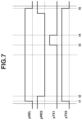
- a photoelectric conversion apparatus according to a second exemplary embodiment will be described with reference to FIG. 7 .
- a configuration different from that of the first exemplary embodiment will be mainly described.
- a different driving timing is employed in the driving method for reading out signal charges at the high FD capacity.
- the second transfer transistor 203 is turned on in a pixel row (first pixel row) where the selection transistor 207 is on, and the second transfer transistor 203 is turned off in a pixel row (second pixel row) where the selection transistor 207 is off.
- Timings of turning on and off the second transfer transistor 203 respectively conform to timings of turning on and off the selection transistor 207 .
- the selection transistor 207 and the second transfer transistor 203 are turned on at the time t 1 and turned off at the time t 5 .
- a dynamic range of the photoelectric conversion apparatus can be expanded, and a punch-through phenomenon can be also prevented from occurring between the photoelectric conversion portion 201 and the FD portion 204 of a pixel arranged in a pixel row where the selection transistor 207 is turned off.
- FIG. 8 is a plan view of pixels according to the present exemplary embodiment.
- FIG. 9 is a circuit diagram illustrating a pixel according to the present exemplary embodiment.
- a configuration different from that of the first exemplary embodiment will be mainly described.
- the second transfer transistor 203 , the FD portion 204 , the reset transistor 205 , the amplification transistor 206 , and the selection transistor 207 are shared by a first photoelectric conversion portion 201 a and a second photoelectric conversion portion 201 b .
- the first photoelectric conversion portion 201 a and the second transfer transistor 203 are connected to each other via a first transfer transistor 202 a (first first-transfer transistor).
- the second photoelectric conversion portion 201 b and the second transfer transistor 203 are connected to each other via a first transfer transistor 202 b (second first-transfer transistor).
- a gate of a single second transfer transistor 203 is in contact with the FD portion 204 . Therefore, a capacity of the gate that is in contact with the FD portion 204 can be reduced in comparison to the case where a plurality of first transfer transistors is in contact with the FD portion 204 , and it is possible to reduce the FD capacity.
- FIG. 10 is an exploded perspective diagram illustrating a photoelectric conversion apparatus 1100 according to the present exemplary embodiment.
- FIGS. 11 A and 11 B are plan views of pixels according to the present exemplary embodiment.
- FIG. 11 A is a plan view viewed from a side (first side) 1110 A of the semiconductor substrate on which the transistors are formed.
- FIG. 11 B is a plan view viewed from a side (second side) 1110 B opposite to the first side of the semiconductor substrate.
- a configuration different from the configuration in the third exemplary embodiment will be described.
- the photoelectric conversion apparatus is a back-side illumination type photoelectric conversion apparatus, on which light is incident from the second side 1110 B.
- a pixel array unit 10110 is arranged on a semiconductor substrate 1110 .
- a control unit 1121 and a signal processing unit 1122 are arranged on another semiconductor substrate 1120 . At least a part of an orthogonal projection of each of the control unit 1121 and the signal processing unit 1122 with respect to the semiconductor substrate 1110 overlaps with the pixel array unit 101 .
- the photoelectric conversion apparatus 1100 according to the present exemplary embodiment may further include another semiconductor substrate including a processing circuit, and three or more semiconductor substrates may be laminated one on top of the other.
- the control unit 1121 may include a vertical scanning circuit for supplying a control signal to the transistor included in the pixel and a power source circuit.
- the control unit 1121 may further include a timing generation circuit for driving the photoelectric conversion apparatus, a reference signal supply circuit for supplying a reference signal to a conversion circuit, and a horizontal scanning circuit for sequentially reading out a signal from an amplification circuit or a conversion circuit.
- the control unit 1121 includes the vertical scanning circuit 102 , the horizontal scanning circuit 104 , and the control circuit 106 in FIG. 1 .
- the signal processing unit 1122 processes an electric signal based on a signal charge generated in a pixel region.
- a noise removal circuit, an amplification circuit, a conversion circuit, and an image signal processing circuit can be included in the signal processing unit 1122 .
- the noise removal circuit is a correlated double sampling (CDS) circuit
- the amplification circuit is a column amplifier circuit.
- the conversion circuit is, for example, an analog-to-digital conversion (ADC) circuit including a comparator and a counter.
- the image signal processing circuit includes a memory and a processor, and generates image data from a digital signal converted through analog-to-digital conversion and executes image processing on the image data.
- the signal processing unit 1122 includes the reading circuit 103 in FIG. 1 .
- FIGS. 11 A and 11 B illustrates an optical center 1001 of a micro lens in a planar view.
- a unit cell includes two photoelectric conversion portions.
- photoelectric conversion portions and a reading circuit for reading from the photoelectric conversion portions corresponding to one optical center are collectively defined as a unit cell.
- the unit cell includes two photoelectric conversion portions overlapping with the micro lens in a planar view, first transfer transistors that control transfer of electric charges from the respective photoelectric conversion portions, a second transfer transistor, an amplification transistor, and a reset transistor.
- the PD portion 204 connected to the second transfer transistor 203 is arranged at a position farthest from the optical center 1001 in the unit cell.
- the FD portion 204 is formed at a corner of the unit cell.
- light is incident on the back side in the back-side illumination type photoelectric conversion apparatus.
- the FD portion 204 is close to the optical center 1001 , there is a high possibility that signal charges photoelectrically converted by the photoelectric conversion portions flow into the PD portion 204 , which can cause lowering of sensitivity and asymmetricity in the incident angle characteristics of the sensitivity.
- the FD portion in a case where the FD portion is shared by a plurality of photoelectric conversion portions, there arises considerable restrictions on the planar arrangement of the FD portion because the FD portion constitutes a part of the first transfer transistor.
- the FD portion in the configuration according to the present exemplary embodiment where the second transfer transistor is added thereto, the FD portion can be arranged with a higher degree of freedom even in a case where the FD portion is shared by a plurality of photoelectric conversion portions.
- FIG. 12 is a block diagram illustrating a configuration of a photoelectric conversion system 1200 according to a fifth exemplary embodiment.
- the photoelectric conversion system 1200 according to the present exemplary embodiment includes a photoelectric conversion apparatus 1204 .
- any of the photoelectric conversion apparatuses described in the above-described exemplary embodiments can be used as the photoelectric conversion apparatus 1204 .
- the photoelectric conversion system 1200 can be used as an image capturing system.
- Specific examples of the photoelectric conversion system 1200 include a digital still camera, a digital camcorder, and a monitoring camera. In FIG. 12 , a digital still camera is illustrated as an example of the photoelectric conversion system 1200 .
- the photoelectric conversion system 1200 in FIG. 12 includes the photoelectric conversion apparatus 1204 , a lens 1202 for forming an optical image of an object on the photoelectric conversion apparatus 1204 , an aperture 1203 for changing the amount of light passing through the lens 1202 , and a barrier 1201 for protecting the lens 1202 .
- the lens 1202 and the aperture 1203 function as an optical system which collects light to the photoelectric conversion apparatus 1204 .
- the photoelectric conversion system 1200 includes a signal processing unit 1205 for processing a signal output from the photoelectric conversion apparatus 1204 .
- the signal processing unit 1205 executes signal processing for executing various types of correction and compression on an input signal as necessary and outputting the processed signal.
- the photoelectric conversion system 1200 further includes a buffer memory unit 1206 for temporarily storing image data and an external interface unit (external I/F unit) 1209 for communicating with an external computer.
- the photoelectric conversion system 1200 includes a recording medium 1211 , such as a semiconductor memory, used for recording or reading captured image data and a recording medium control I/F unit 1210 for executing recording or reading processing on the recording medium 1211 .
- the recording medium 1211 may be built into the photoelectric conversion system 1200 , or may be detachably attached to the photoelectric conversion system 1200 . Further, the recording medium control I/F unit 1210 may wirelessly communicate with the recording medium 1211 and the external I/F unit 1209 .
- the photoelectric conversion system 1200 further includes a general control/calculation unit 1208 for executing various calculations and controlling the entirety of the digital still camera and a timing generation unit 1207 for outputting various timing signals to the photoelectric conversion apparatus 1204 and the signal processing unit 1205 .
- a timing signal may be received from an external unit, and the photoelectric conversion system 1200 may include at least the photoelectric conversion apparatus 1204 and the signal processing unit 1205 for processing the output signal output from the photoelectric conversion apparatus 1204 .
- the timing generation unit 1207 may be mounted on the photoelectric conversion apparatus 1204 .
- the general control/calculation unit 1208 and the timing generation unit 1207 may be configured to execute all or a part of the control function of the photoelectric conversion apparatus 1204 .
- the photoelectric conversion apparatus 1204 outputs an image signal to the signal processing unit 1205 .
- the signal processing unit 1205 executes predetermined signal processing on the image signal output from the photoelectric conversion apparatus 1204 and outputs image data.
- the signal processing unit 1205 also generates an image by using the image signal.
- the signal processing unit 1205 and the timing generation unit 1207 may be mounted on the photoelectric conversion apparatus 1204 .
- the signal processing unit 1205 and the timing generation unit 1207 may be mounted on a substrate where pixels are arranged, or may be mounted on another substrate as described in the third exemplary embodiment.
- FIGS. 13 A, 13 B, and 14 are diagrams schematically illustrating configuration examples of the photoelectric conversion system and the moving body according to the present exemplary embodiment.
- FIG. 14 is a flowchart illustrating processing of the photoelectric conversion system according to the present exemplary embodiment.
- an in-vehicle camera will be described as an example of the photoelectric conversion system.
- FIGS. 13 A and 13 B are diagrams illustrating examples of a vehicle system and a photoelectric conversion system for executing image capturing, mounted on the vehicle system.
- a photoelectric conversion system 1301 includes a photoelectric conversion apparatus 1302 , an image pre-processing unit 1315 , an integrated circuit 1303 , and an optical system 1314 .
- the optical system 1314 forms an optical image of an object on the photoelectric conversion apparatus 1302 .
- the photoelectric conversion apparatus 1302 converts the optical image of the object formed by the optical system 1314 to an electric signal.
- the photoelectric conversion apparatus 1302 is the photoelectric conversion apparatus according to any one of the above-described exemplary embodiments.
- the image pre-processing unit 1315 executes predetermined signal processing on the signal output from the photoelectric conversion apparatus 1302 .
- Functions of the image pre-processing unit 1315 may be embedded in the photoelectric conversion apparatus 1302 .
- At least two sets of components, each of which includes the optical system 1314 , the photoelectric conversion apparatus 1302 , and the image pre-processing unit 1315 are arranged on the photoelectric conversion system 1301 , and signals output from the image pre-processing units 1315 of respective sets are input to the integrated circuit 1303 .
- the integrated circuit 1303 is an integrated circuit directed to use for an image capturing system, and includes an image processing unit 1304 including a memory 1305 , an optical range-finding unit 1306 , a disparity calculation unit 1307 , an object recognition unit 1308 , and an abnormality detection unit 1309 .
- the image processing unit 1304 executes image processing, such as development processing and defect correction processing, with respect to a signal output from the image pre-processing unit 1315 .
- the memory 1305 temporarily stores a captured image, and stores a defect position of an image capturing pixel.
- the optical range-finding unit 1306 executes focusing and range-finding processing of the object.
- the disparity calculation unit 1307 calculates disparity information (a phase difference of disparity images) from a plurality of pieces of image data acquired by the plurality of photoelectric conversion apparatuses 1302 .
- the object recognition unit 1308 executes recognition of objects such as a vehicle, a street, a traffic sign, and a person.
- the abnormality detection unit 1309 detects abnormality of the photoelectric conversion apparatus 1302 to notify a main control unit 1313 of the abnormality.
- the integrated circuit 1303 may be realized by the hardware designed for dedicated use or a software module, or may be realized by a combination thereof. Further, the integrated circuit 1303 may be realized by a field programmable gate array (FPGA) or an application specific integrated circuit (ASIC), or may be realized by a combination thereof.
- FPGA field programmable gate array
- ASIC application specific integrated circuit
- the main control unit 1313 manages and controls the operations executed by the photoelectric conversion system 1301 , a vehicle sensor 1310 , and a control unit 1320 .
- a method according to a standard of the controller area network (CAN) can be also employed.
- each of the photoelectric conversion system 1301 , the vehicle sensor 1310 , and the control unit 1320 individually includes a communication interface and executes transmission and reception of the control signal via a communication network.
- the integrated circuit 1303 has functions of transmitting a control signal or a setting value to the photoelectric conversion apparatus 1302 by receiving a control signal from the main control unit 1313 or by a control unit thereof.
- the photoelectric conversion system 1301 is connected to the vehicle sensor 1310 , and can detect a running condition of its own vehicle (e.g., a vehicle speed, a yaw rate, and a rudder angle), an environment outside its own vehicle, and a state of another vehicle or an obstacle.
- the vehicle sensor 1310 also serves as a distance information acquisition unit which acquires distance information indicating a distance to a target object from a parallax image.
- the photoelectric conversion system 1301 is connected to a drive assist control unit 1311 which executes various drive assisting functions, such as an auto-steering function, an auto-cruising function, and a collision prevention function.
- a collision determination unit estimates or determines occurrence of collision with another vehicle or an obstacle based on the detection results acquired by the photoelectric conversion system 1301 and the vehicle sensor 1310 .
- collision-avoidance control is executed in a case where occurrence of collision is expected, and a safety apparatus is activated in a case where collision occurs.
- the photoelectric conversion system 1301 is also connected to an alarming apparatus 1312 which sends an alert to a driver based on a determination result acquired by the collision determination unit. For example, in a case where the determination result acquired by the collision determination unit indicates that a chance of collision is high, the main control unit 1313 executes vehicle control for avoiding a collision or reducing damage by applying a brake, releasing an accelerator, and reducing an engine output.
- the alarming apparatus 1312 provides a warning by making alarm sound, displaying alarming information on a display screen of a car navigation system or a dashboard meter panel, or producing vibrations in a seat belt or a steering wheel.
- the photoelectric conversion system 1301 captures images around vehicle, e.g., a forward view and a backward view of a vehicle.
- FIG. 13 B is a diagram illustrating an example of arrangement of the photoelectric conversion system 1301 when a forward view of the vehicle is to be captured thereby.
- the two photoelectric conversion apparatuses 1302 are arranged on a front side of the vehicle 1300 .
- a center line in a back-and-forth direction of the vehicle 1300 or a center line with respect to an external shape (e.g., vehicle width) is taken as a symmetrical axis, and the two photoelectric conversion apparatuses 1302 are arranged line-symmetrically with respect to the symmetrical axis, which is desirable in acquisition of information about a distance between the vehicle 1300 and a target object or determination on a chance of collision.
- each of the photoelectric conversion apparatuses 1302 be arranged not to disturb a driver's field of view when the driver visually checks the surroundings outside the vehicle 1300 from a driver's seat.
- the alarming apparatus 1312 be arranged at a position where the alarming apparatus 1312 can easily enter the driver's field of view.
- the failure detection operation of the photoelectric conversion apparatus 1302 in the photoelectric conversion system 1301 is executed according to steps S 1410 to S 1480 illustrated in FIG. 14 .
- step S 1410 a setting for starting the photoelectric conversion apparatus 1302 is executed.
- an operation setting of the photoelectric conversion apparatus 1302 is transmitted from an external portion (e.g., the main control unit 1313 ) or an internal portion of the photoelectric conversion system 1301 , so that an image capturing operation and a failure detection operation of the photoelectric conversion apparatus 1302 are started.
- step S 1420 the photoelectric conversion system 1301 acquires a pixel signal from an effective pixel. Further, in step S 1430 , the photoelectric conversion system 1301 acquires a value output from a failure detection pixel arranged for the failure detection. Similar to the effective pixel, the failure detection pixel also includes a photoelectric conversion portion. A predetermined voltage is written into this photoelectric conversion portion. The failure detection pixel outputs a signal corresponding to the voltage written into the photoelectric conversion portion.
- the processing in steps S 1420 and S 1430 may be executed in reverse order.
- step S 1440 the photoelectric conversion system 1301 executes conformity/non-conformity determination of a value actually output from the failure detection pixel and an expected output value thereof.
- the processing proceeds to step S 1450 .
- step S 1450 the photoelectric conversion system 1301 determines that the image capturing operation is executed normally, and the processing then proceeds to step S 1460 .
- step S 1460 the photoelectric conversion system 1301 transmits a pixel signal of the scanning row and temporarily stores the pixel signal in the memory 1305 .
- step S 1440 the photoelectric conversion system 1301 determines that abnormality has occurred in the image capturing operation, and sends an alert to the main control unit 1313 or the alarming apparatus 1312 .
- the alarming apparatus 1312 displays information about detection of abnormality on a display unit.
- step S 1480 the photoelectric conversion apparatus 1302 is stopped, and processing of the photoelectric conversion system 1301 is ended.
- the processing in the flowchart is repeated for each row.
- the processing in the flowchart may be repeated for a plurality of rows, or the failure detection may be executed for each frame.
- an alert may be issued to the outside of the vehicle via a wireless network.
- the disclosure is also applicable to control of automatically driving a vehicle to follow another vehicle or control of automatically driving a vehicle not to drift from a traffic lane.
- the photoelectric conversion system 1301 is applicable not only to a vehicle such as an automobile but also to a moving body (moving apparatus) such as a ship, an airplane, or an industrial robot.
- the photoelectric conversion system 1301 is applicable to a device such as an intelligent transportation system (ITS), which widely employs an object recognition function.
- ITS intelligent transportation system
- the photoelectric conversion apparatuses according to the exemplary embodiments of the disclosure may further include a color filter or a micro lens, and may be configured to acquire various types of information such as distance information.
- the amplification transistor is provided as a part of the source follower circuit, the amplification transistor may constitute a part of the AD conversion unit. Specifically, the amplification transistor may constitute a part of a comparator included in the AD conversion unit. Further, a part of the constituent elements of the comparator may be arranged on another semiconductor substrate.
- the disclosure is not limited to the above exemplary embodiments, and many variations are possible.
- an example in which a part of a configuration according to any of the above-described exemplary embodiments is added to or replaced with a configuration according to another exemplary embodiment is also included in the exemplary embodiments of the disclosure.
- the above-described exemplary embodiments are merely examples embodying the disclosure, and shall not be construed as limiting the technical scope of the disclosure.
- the present disclosure can be realized in various ways without departing from the technical spirit or main features of the disclosure.
- lowering of the reset performance of the input node can be prevented, and, at the same time, a dynamic range of the photoelectric conversion apparatus can be expanded.
Landscapes
- Engineering & Computer Science (AREA)
- Multimedia (AREA)
- Signal Processing (AREA)
- Solid State Image Pick-Up Elements (AREA)
- Transforming Light Signals Into Electric Signals (AREA)
Applications Claiming Priority (2)
| Application Number | Priority Date | Filing Date | Title |
|---|---|---|---|
| JP2019121950A JP2021010075A (ja) | 2019-06-28 | 2019-06-28 | 光電変換装置、光電変換システム、および移動体 |
| JP2019-121950 | 2019-06-28 |
Publications (2)
| Publication Number | Publication Date |
|---|---|
| US20200411572A1 US20200411572A1 (en) | 2020-12-31 |
| US11776974B2 true US11776974B2 (en) | 2023-10-03 |
Family
ID=74043801
Family Applications (1)
| Application Number | Title | Priority Date | Filing Date |
|---|---|---|---|
| US16/912,394 Active 2040-07-17 US11776974B2 (en) | 2019-06-28 | 2020-06-25 | Photoelectric conversion apparatus, photoelectric conversion system, and moving body |
Country Status (2)
| Country | Link |
|---|---|
| US (1) | US11776974B2 (enExample) |
| JP (2) | JP2021010075A (enExample) |
Cited By (1)
| Publication number | Priority date | Publication date | Assignee | Title |
|---|---|---|---|---|
| US12407957B1 (en) * | 2022-12-22 | 2025-09-02 | Apple Inc. | Multiple-substrate high conversion gain pixels |
Families Citing this family (3)
| Publication number | Priority date | Publication date | Assignee | Title |
|---|---|---|---|---|
| JP2017183563A (ja) | 2016-03-31 | 2017-10-05 | ソニー株式会社 | 撮像装置、駆動方法、および、電子機器 |
| WO2024031300A1 (en) * | 2022-08-09 | 2024-02-15 | Huawei Technologies Co., Ltd. | Photon counting pixel and method of operation thereof |
| DE102022125838A1 (de) * | 2022-10-06 | 2024-04-11 | Arnold & Richter Cine Technik Gmbh & Co. Betriebs Kg | Bildsensor |
Citations (12)
| Publication number | Priority date | Publication date | Assignee | Title |
|---|---|---|---|---|
| US20060219868A1 (en) * | 2005-03-29 | 2006-10-05 | Konica Minolta Holdings, Inc. | Solid-state image-sensing device |
| US20080173909A1 (en) | 2007-01-19 | 2008-07-24 | Christopher Parks | Image sensor with gain control |
| US20090045319A1 (en) | 2005-04-07 | 2009-02-19 | Tohoku University | Optical Sensor, Solid-State Imaging Device, and Operating Method of Solid-State Imaging Device |
| US20120327278A1 (en) * | 2008-04-03 | 2012-12-27 | Sony Corporation | Solid state imaging device, driving method of the solid state imaging device, and electronic equipment |
| US8648939B2 (en) * | 2009-07-23 | 2014-02-11 | Sony Corporation | Solid-state imaging device, drive method therefor, and electronic device |
| US8917341B2 (en) * | 2010-02-26 | 2014-12-23 | Sony Corporation | Solid-state image pickup apparatus, driving method for solid-state image pickup apparatus and electronic device |
| US9060145B2 (en) * | 2010-03-11 | 2015-06-16 | Sony Corporation | Solid-state image taking apparatus, method for driving solid-state image taking apparatus and electronic apparatus |
| JP2015233185A (ja) | 2014-06-09 | 2015-12-24 | 株式会社東芝 | 固体撮像装置 |
| US20170353675A1 (en) | 2016-06-06 | 2017-12-07 | Canon Kabushiki Kaisha | Imaging apparatus, imaging system, and moving object |
| US20180376083A1 (en) | 2016-02-15 | 2018-12-27 | Panasonic Intellectual Property Management Co., Ltd. | Solid-state imaging device and imaging apparatus |
| US20200185435A1 (en) * | 2018-12-11 | 2020-06-11 | Canon Kabushiki Kaisha | Photoelectric conversion apparatus and image pickup system |
| US20200404199A1 (en) * | 2017-11-20 | 2020-12-24 | Ecole Polytechnique Fédérale De Lausanne Epfl-Tto | Pixel Sensor Cell for CMOS Image Sensors with Enhanced Conversion Gain at High Dynamic Range Capability |
Family Cites Families (4)
| Publication number | Priority date | Publication date | Assignee | Title |
|---|---|---|---|---|
| JP2014222797A (ja) * | 2013-05-13 | 2014-11-27 | ソニー株式会社 | 固体撮像素子、固体撮像素子の駆動方法、及び、電子機器 |
| JP2015220577A (ja) * | 2014-05-16 | 2015-12-07 | 株式会社東芝 | 固体撮像装置 |
| JP2017054966A (ja) * | 2015-09-10 | 2017-03-16 | ルネサスエレクトロニクス株式会社 | 半導体装置の製造方法および半導体装置 |
| JP2018186398A (ja) * | 2017-04-26 | 2018-11-22 | ソニーセミコンダクタソリューションズ株式会社 | 固体撮像装置、および電子機器 |
-
2019
- 2019-06-28 JP JP2019121950A patent/JP2021010075A/ja not_active Ceased
-
2020
- 2020-06-25 US US16/912,394 patent/US11776974B2/en active Active
-
2023
- 2023-10-31 JP JP2023187256A patent/JP7639097B2/ja active Active
Patent Citations (12)
| Publication number | Priority date | Publication date | Assignee | Title |
|---|---|---|---|---|
| US20060219868A1 (en) * | 2005-03-29 | 2006-10-05 | Konica Minolta Holdings, Inc. | Solid-state image-sensing device |
| US20090045319A1 (en) | 2005-04-07 | 2009-02-19 | Tohoku University | Optical Sensor, Solid-State Imaging Device, and Operating Method of Solid-State Imaging Device |
| US20080173909A1 (en) | 2007-01-19 | 2008-07-24 | Christopher Parks | Image sensor with gain control |
| US20120327278A1 (en) * | 2008-04-03 | 2012-12-27 | Sony Corporation | Solid state imaging device, driving method of the solid state imaging device, and electronic equipment |
| US8648939B2 (en) * | 2009-07-23 | 2014-02-11 | Sony Corporation | Solid-state imaging device, drive method therefor, and electronic device |
| US8917341B2 (en) * | 2010-02-26 | 2014-12-23 | Sony Corporation | Solid-state image pickup apparatus, driving method for solid-state image pickup apparatus and electronic device |
| US9060145B2 (en) * | 2010-03-11 | 2015-06-16 | Sony Corporation | Solid-state image taking apparatus, method for driving solid-state image taking apparatus and electronic apparatus |
| JP2015233185A (ja) | 2014-06-09 | 2015-12-24 | 株式会社東芝 | 固体撮像装置 |
| US20180376083A1 (en) | 2016-02-15 | 2018-12-27 | Panasonic Intellectual Property Management Co., Ltd. | Solid-state imaging device and imaging apparatus |
| US20170353675A1 (en) | 2016-06-06 | 2017-12-07 | Canon Kabushiki Kaisha | Imaging apparatus, imaging system, and moving object |
| US20200404199A1 (en) * | 2017-11-20 | 2020-12-24 | Ecole Polytechnique Fédérale De Lausanne Epfl-Tto | Pixel Sensor Cell for CMOS Image Sensors with Enhanced Conversion Gain at High Dynamic Range Capability |
| US20200185435A1 (en) * | 2018-12-11 | 2020-06-11 | Canon Kabushiki Kaisha | Photoelectric conversion apparatus and image pickup system |
Cited By (1)
| Publication number | Priority date | Publication date | Assignee | Title |
|---|---|---|---|---|
| US12407957B1 (en) * | 2022-12-22 | 2025-09-02 | Apple Inc. | Multiple-substrate high conversion gain pixels |
Also Published As
| Publication number | Publication date |
|---|---|
| JP2021010075A (ja) | 2021-01-28 |
| JP2024012454A (ja) | 2024-01-30 |
| US20200411572A1 (en) | 2020-12-31 |
| JP7639097B2 (ja) | 2025-03-04 |
Similar Documents
| Publication | Publication Date | Title |
|---|---|---|
| US11159759B2 (en) | Solid-state imaging device, method of driving solid-state imaging device, and imaging system that can detect a failure while performing capturing | |
| US11770629B2 (en) | Solid-state imaging element and imaging device | |
| US11776974B2 (en) | Photoelectric conversion apparatus, photoelectric conversion system, and moving body | |
| US11303829B2 (en) | Imaging device and drive method of imaging device | |
| US20180197907A1 (en) | Solid-state imaging device and imaging system | |
| US10789724B2 (en) | Imaging apparatus, imaging system, moving body, and semiconductor substrate for lamination | |
| US11937001B2 (en) | Sensor and control method | |
| US11265493B2 (en) | Imaging sensor, imaging system, and moving body | |
| US11140348B2 (en) | AD conversion device, imaging device, imaging system, and mobile apparatus | |
| US12120447B2 (en) | Photoelectric conversion device, imaging system, moving body, and stackable semiconductor device | |
| CN110226325B (zh) | 摄像系统和摄像装置 | |
| JP7297546B2 (ja) | 光電変換装置、撮像システム、移動体、および積層用の半導体基板 | |
| US10469762B2 (en) | Image pickup device, image pickup system, and movable body | |
| US11258966B2 (en) | Photoelectric conversion device, camera, movable object, and signal processing device | |
| US11509886B2 (en) | Photoelectric conversion device and photoelectric conversion system | |
| US10930690B2 (en) | Photoelectric conversion apparatus, photoelectric conversion system, and movable body | |
| JP6812397B2 (ja) | 固体撮像装置及びその駆動方法、並びに撮像システム | |
| KR102754436B1 (ko) | 고체 촬상 소자 및 전자 기기 | |
| EP4525477A1 (en) | Photoelectric conversion device, movable apparatus, control method, and storage medium | |
| WO2023100547A1 (ja) | 撮像装置および電子機器 |
Legal Events
| Date | Code | Title | Description |
|---|---|---|---|
| FEPP | Fee payment procedure |
Free format text: ENTITY STATUS SET TO UNDISCOUNTED (ORIGINAL EVENT CODE: BIG.); ENTITY STATUS OF PATENT OWNER: LARGE ENTITY |
|
| AS | Assignment |
Owner name: CANON KABUSHIKI KAISHA, JAPAN Free format text: ASSIGNMENT OF ASSIGNORS INTEREST;ASSIGNOR:SEKINE, HIROSHI;REEL/FRAME:053701/0390 Effective date: 20200609 |
|
| STPP | Information on status: patent application and granting procedure in general |
Free format text: DOCKETED NEW CASE - READY FOR EXAMINATION |
|
| STPP | Information on status: patent application and granting procedure in general |
Free format text: NON FINAL ACTION MAILED |
|
| STPP | Information on status: patent application and granting procedure in general |
Free format text: RESPONSE TO NON-FINAL OFFICE ACTION ENTERED AND FORWARDED TO EXAMINER |
|
| STPP | Information on status: patent application and granting procedure in general |
Free format text: FINAL REJECTION MAILED |
|
| STPP | Information on status: patent application and granting procedure in general |
Free format text: RESPONSE AFTER FINAL ACTION FORWARDED TO EXAMINER |
|
| STPP | Information on status: patent application and granting procedure in general |
Free format text: ADVISORY ACTION MAILED |
|
| STPP | Information on status: patent application and granting procedure in general |
Free format text: AWAITING TC RESP., ISSUE FEE NOT PAID |
|
| STPP | Information on status: patent application and granting procedure in general |
Free format text: NOTICE OF ALLOWANCE MAILED -- APPLICATION RECEIVED IN OFFICE OF PUBLICATIONS |
|
| STPP | Information on status: patent application and granting procedure in general |
Free format text: PUBLICATIONS -- ISSUE FEE PAYMENT VERIFIED |
|
| STCF | Information on status: patent grant |
Free format text: PATENTED CASE |