US11756872B2 - Package structure and manufacturing method thereof - Google Patents
Package structure and manufacturing method thereof Download PDFInfo
- Publication number
- US11756872B2 US11756872B2 US17/199,348 US202117199348A US11756872B2 US 11756872 B2 US11756872 B2 US 11756872B2 US 202117199348 A US202117199348 A US 202117199348A US 11756872 B2 US11756872 B2 US 11756872B2
- Authority
- US
- United States
- Prior art keywords
- insulating body
- carrier substrate
- die
- tcv
- tcvs
- Prior art date
- Legal status (The legal status is an assumption and is not a legal conclusion. Google has not performed a legal analysis and makes no representation as to the accuracy of the status listed.)
- Active, expires
Links
- 238000004519 manufacturing process Methods 0.000 title claims description 27
- 239000000758 substrate Substances 0.000 claims abstract description 166
- 241000711508 Turkey coronavirus Species 0.000 claims abstract description 127
- 238000000034 method Methods 0.000 claims description 134
- 239000000463 material Substances 0.000 claims description 68
- 239000008393 encapsulating agent Substances 0.000 claims description 36
- 241000701384 Tipula iridescent virus Species 0.000 claims description 23
- 239000004020 conductor Substances 0.000 claims description 14
- 230000000149 penetrating effect Effects 0.000 claims 1
- 230000008569 process Effects 0.000 description 117
- 239000010410 layer Substances 0.000 description 115
- 238000005530 etching Methods 0.000 description 33
- 239000012790 adhesive layer Substances 0.000 description 14
- 239000004065 semiconductor Substances 0.000 description 14
- 238000000465 moulding Methods 0.000 description 11
- 238000007747 plating Methods 0.000 description 10
- 229910052802 copper Inorganic materials 0.000 description 9
- 239000010949 copper Substances 0.000 description 9
- 239000000523 sample Substances 0.000 description 8
- 238000012360 testing method Methods 0.000 description 8
- RYGMFSIKBFXOCR-UHFFFAOYSA-N Copper Chemical compound [Cu] RYGMFSIKBFXOCR-UHFFFAOYSA-N 0.000 description 7
- 238000000227 grinding Methods 0.000 description 7
- PXHVJJICTQNCMI-UHFFFAOYSA-N Nickel Chemical compound [Ni] PXHVJJICTQNCMI-UHFFFAOYSA-N 0.000 description 6
- 230000015572 biosynthetic process Effects 0.000 description 6
- 150000001875 compounds Chemical class 0.000 description 6
- 239000000945 filler Substances 0.000 description 6
- 239000011810 insulating material Substances 0.000 description 6
- RTAQQCXQSZGOHL-UHFFFAOYSA-N Titanium Chemical compound [Ti] RTAQQCXQSZGOHL-UHFFFAOYSA-N 0.000 description 5
- 238000009713 electroplating Methods 0.000 description 5
- 230000007246 mechanism Effects 0.000 description 5
- 239000010936 titanium Substances 0.000 description 5
- 229910052719 titanium Inorganic materials 0.000 description 5
- VYPSYNLAJGMNEJ-UHFFFAOYSA-N Silicium dioxide Chemical compound O=[Si]=O VYPSYNLAJGMNEJ-UHFFFAOYSA-N 0.000 description 4
- 229910045601 alloy Inorganic materials 0.000 description 4
- 239000000956 alloy Substances 0.000 description 4
- 238000005553 drilling Methods 0.000 description 4
- 229920002120 photoresistant polymer Polymers 0.000 description 4
- 238000005240 physical vapour deposition Methods 0.000 description 4
- 239000004642 Polyimide Substances 0.000 description 3
- 229910052581 Si3N4 Inorganic materials 0.000 description 3
- UMIVXZPTRXBADB-UHFFFAOYSA-N benzocyclobutene Chemical compound C1=CC=C2CCC2=C1 UMIVXZPTRXBADB-UHFFFAOYSA-N 0.000 description 3
- 238000005229 chemical vapour deposition Methods 0.000 description 3
- 238000005520 cutting process Methods 0.000 description 3
- 238000007772 electroless plating Methods 0.000 description 3
- 238000007654 immersion Methods 0.000 description 3
- 238000003698 laser cutting Methods 0.000 description 3
- 229910052759 nickel Inorganic materials 0.000 description 3
- TWNQGVIAIRXVLR-UHFFFAOYSA-N oxo(oxoalumanyloxy)alumane Chemical compound O=[Al]O[Al]=O TWNQGVIAIRXVLR-UHFFFAOYSA-N 0.000 description 3
- 238000004806 packaging method and process Methods 0.000 description 3
- 229920002577 polybenzoxazole Polymers 0.000 description 3
- 229920001721 polyimide Polymers 0.000 description 3
- HQVNEWCFYHHQES-UHFFFAOYSA-N silicon nitride Chemical compound N12[Si]34N5[Si]62N3[Si]51N64 HQVNEWCFYHHQES-UHFFFAOYSA-N 0.000 description 3
- 238000012795 verification Methods 0.000 description 3
- QTBSBXVTEAMEQO-UHFFFAOYSA-M Acetate Chemical compound CC([O-])=O QTBSBXVTEAMEQO-UHFFFAOYSA-M 0.000 description 2
- 239000004677 Nylon Substances 0.000 description 2
- 239000004698 Polyethylene Substances 0.000 description 2
- 239000004793 Polystyrene Substances 0.000 description 2
- DHKHKXVYLBGOIT-UHFFFAOYSA-N acetaldehyde Diethyl Acetal Natural products CCOC(C)OCC DHKHKXVYLBGOIT-UHFFFAOYSA-N 0.000 description 2
- 125000002777 acetyl group Chemical class [H]C([H])([H])C(*)=O 0.000 description 2
- NIXOWILDQLNWCW-UHFFFAOYSA-N acrylic acid group Chemical group C(C=C)(=O)O NIXOWILDQLNWCW-UHFFFAOYSA-N 0.000 description 2
- 229910052782 aluminium Inorganic materials 0.000 description 2
- XAGFODPZIPBFFR-UHFFFAOYSA-N aluminium Chemical compound [Al] XAGFODPZIPBFFR-UHFFFAOYSA-N 0.000 description 2
- VXAUWWUXCIMFIM-UHFFFAOYSA-M aluminum;oxygen(2-);hydroxide Chemical compound [OH-].[O-2].[Al+3] VXAUWWUXCIMFIM-UHFFFAOYSA-M 0.000 description 2
- 238000000231 atomic layer deposition Methods 0.000 description 2
- 239000001913 cellulose Substances 0.000 description 2
- 229920002678 cellulose Polymers 0.000 description 2
- 238000000748 compression moulding Methods 0.000 description 2
- 239000011521 glass Substances 0.000 description 2
- 230000006872 improvement Effects 0.000 description 2
- 230000010354 integration Effects 0.000 description 2
- 229910052745 lead Inorganic materials 0.000 description 2
- 239000011133 lead Substances 0.000 description 2
- 229920001778 nylon Polymers 0.000 description 2
- 239000011368 organic material Substances 0.000 description 2
- 239000012188 paraffin wax Substances 0.000 description 2
- 239000002245 particle Substances 0.000 description 2
- 238000000623 plasma-assisted chemical vapour deposition Methods 0.000 description 2
- 229920000728 polyester Polymers 0.000 description 2
- -1 polyethylene Polymers 0.000 description 2
- 229920000573 polyethylene Polymers 0.000 description 2
- 229920000098 polyolefin Polymers 0.000 description 2
- 229920001296 polysiloxane Polymers 0.000 description 2
- 229920002223 polystyrene Polymers 0.000 description 2
- 229920005989 resin Polymers 0.000 description 2
- 239000011347 resin Substances 0.000 description 2
- HBMJWWWQQXIZIP-UHFFFAOYSA-N silicon carbide Chemical compound [Si+]#[C-] HBMJWWWQQXIZIP-UHFFFAOYSA-N 0.000 description 2
- 239000000377 silicon dioxide Substances 0.000 description 2
- 229910052709 silver Inorganic materials 0.000 description 2
- 239000010944 silver (metal) Substances 0.000 description 2
- 238000004544 sputter deposition Methods 0.000 description 2
- 229910052718 tin Inorganic materials 0.000 description 2
- 239000011135 tin Substances 0.000 description 2
- 238000001721 transfer moulding Methods 0.000 description 2
- WFKWXMTUELFFGS-UHFFFAOYSA-N tungsten Chemical compound [W] WFKWXMTUELFFGS-UHFFFAOYSA-N 0.000 description 2
- 229910052721 tungsten Inorganic materials 0.000 description 2
- 239000010937 tungsten Substances 0.000 description 2
- 125000000391 vinyl group Chemical group [H]C([*])=C([H])[H] 0.000 description 2
- 229920002554 vinyl polymer Polymers 0.000 description 2
- PIGFYZPCRLYGLF-UHFFFAOYSA-N Aluminum nitride Chemical compound [Al]#N PIGFYZPCRLYGLF-UHFFFAOYSA-N 0.000 description 1
- 229910000881 Cu alloy Inorganic materials 0.000 description 1
- 239000004593 Epoxy Substances 0.000 description 1
- NRTOMJZYCJJWKI-UHFFFAOYSA-N Titanium nitride Chemical compound [Ti]#N NRTOMJZYCJJWKI-UHFFFAOYSA-N 0.000 description 1
- 239000002318 adhesion promoter Substances 0.000 description 1
- 230000004075 alteration Effects 0.000 description 1
- 239000003990 capacitor Substances 0.000 description 1
- 239000000919 ceramic Substances 0.000 description 1
- 239000003795 chemical substances by application Substances 0.000 description 1
- 239000002131 composite material Substances 0.000 description 1
- 238000010276 construction Methods 0.000 description 1
- PMHQVHHXPFUNSP-UHFFFAOYSA-M copper(1+);methylsulfanylmethane;bromide Chemical compound Br[Cu].CSC PMHQVHHXPFUNSP-UHFFFAOYSA-M 0.000 description 1
- 239000003989 dielectric material Substances 0.000 description 1
- 239000003822 epoxy resin Substances 0.000 description 1
- 238000005429 filling process Methods 0.000 description 1
- 229910052732 germanium Inorganic materials 0.000 description 1
- GNPVGFCGXDBREM-UHFFFAOYSA-N germanium atom Chemical compound [Ge] GNPVGFCGXDBREM-UHFFFAOYSA-N 0.000 description 1
- 229910010272 inorganic material Inorganic materials 0.000 description 1
- 239000011147 inorganic material Substances 0.000 description 1
- 239000007769 metal material Substances 0.000 description 1
- 230000000737 periodic effect Effects 0.000 description 1
- 238000005498 polishing Methods 0.000 description 1
- 229920000647 polyepoxide Polymers 0.000 description 1
- 229920000642 polymer Polymers 0.000 description 1
- 230000009467 reduction Effects 0.000 description 1
- 238000005096 rolling process Methods 0.000 description 1
- 229910052710 silicon Inorganic materials 0.000 description 1
- 239000010703 silicon Substances 0.000 description 1
- 229910010271 silicon carbide Inorganic materials 0.000 description 1
- 229910000679 solder Inorganic materials 0.000 description 1
- 238000003892 spreading Methods 0.000 description 1
- 230000007480 spreading Effects 0.000 description 1
- 239000000126 substance Substances 0.000 description 1
- 238000006467 substitution reaction Methods 0.000 description 1
- 229910052715 tantalum Inorganic materials 0.000 description 1
- GUVRBAGPIYLISA-UHFFFAOYSA-N tantalum atom Chemical compound [Ta] GUVRBAGPIYLISA-UHFFFAOYSA-N 0.000 description 1
- MZLGASXMSKOWSE-UHFFFAOYSA-N tantalum nitride Chemical compound [Ta]#N MZLGASXMSKOWSE-UHFFFAOYSA-N 0.000 description 1
Images


Classifications
-
- H—ELECTRICITY
- H01—ELECTRIC ELEMENTS
- H01L—SEMICONDUCTOR DEVICES NOT COVERED BY CLASS H10
- H01L23/00—Details of semiconductor or other solid state devices
- H01L23/48—Arrangements for conducting electric current to or from the solid state body in operation, e.g. leads, terminal arrangements ; Selection of materials therefor
- H01L23/488—Arrangements for conducting electric current to or from the solid state body in operation, e.g. leads, terminal arrangements ; Selection of materials therefor consisting of soldered or bonded constructions
- H01L23/498—Leads, i.e. metallisations or lead-frames on insulating substrates, e.g. chip carriers
- H01L23/49838—Geometry or layout
-
- H—ELECTRICITY
- H01—ELECTRIC ELEMENTS
- H01L—SEMICONDUCTOR DEVICES NOT COVERED BY CLASS H10
- H01L23/00—Details of semiconductor or other solid state devices
- H01L23/48—Arrangements for conducting electric current to or from the solid state body in operation, e.g. leads, terminal arrangements ; Selection of materials therefor
- H01L23/488—Arrangements for conducting electric current to or from the solid state body in operation, e.g. leads, terminal arrangements ; Selection of materials therefor consisting of soldered or bonded constructions
- H01L23/498—Leads, i.e. metallisations or lead-frames on insulating substrates, e.g. chip carriers
- H01L23/49827—Via connections through the substrates, e.g. pins going through the substrate, coaxial cables
-
- H—ELECTRICITY
- H01—ELECTRIC ELEMENTS
- H01L—SEMICONDUCTOR DEVICES NOT COVERED BY CLASS H10
- H01L21/00—Processes or apparatus adapted for the manufacture or treatment of semiconductor or solid state devices or of parts thereof
- H01L21/67—Apparatus specially adapted for handling semiconductor or electric solid state devices during manufacture or treatment thereof; Apparatus specially adapted for handling wafers during manufacture or treatment of semiconductor or electric solid state devices or components ; Apparatus not specifically provided for elsewhere
- H01L21/683—Apparatus specially adapted for handling semiconductor or electric solid state devices during manufacture or treatment thereof; Apparatus specially adapted for handling wafers during manufacture or treatment of semiconductor or electric solid state devices or components ; Apparatus not specifically provided for elsewhere for supporting or gripping
- H01L21/6835—Apparatus specially adapted for handling semiconductor or electric solid state devices during manufacture or treatment thereof; Apparatus specially adapted for handling wafers during manufacture or treatment of semiconductor or electric solid state devices or components ; Apparatus not specifically provided for elsewhere for supporting or gripping using temporarily an auxiliary support
-
- H—ELECTRICITY
- H01—ELECTRIC ELEMENTS
- H01L—SEMICONDUCTOR DEVICES NOT COVERED BY CLASS H10
- H01L21/00—Processes or apparatus adapted for the manufacture or treatment of semiconductor or solid state devices or of parts thereof
- H01L21/02—Manufacture or treatment of semiconductor devices or of parts thereof
- H01L21/04—Manufacture or treatment of semiconductor devices or of parts thereof the devices having potential barriers, e.g. a PN junction, depletion layer or carrier concentration layer
- H01L21/48—Manufacture or treatment of parts, e.g. containers, prior to assembly of the devices, using processes not provided for in a single one of the subgroups H01L21/06 - H01L21/326
- H01L21/4814—Conductive parts
- H01L21/4846—Leads on or in insulating or insulated substrates, e.g. metallisation
- H01L21/4857—Multilayer substrates
-
- H—ELECTRICITY
- H01—ELECTRIC ELEMENTS
- H01L—SEMICONDUCTOR DEVICES NOT COVERED BY CLASS H10
- H01L21/00—Processes or apparatus adapted for the manufacture or treatment of semiconductor or solid state devices or of parts thereof
- H01L21/02—Manufacture or treatment of semiconductor devices or of parts thereof
- H01L21/04—Manufacture or treatment of semiconductor devices or of parts thereof the devices having potential barriers, e.g. a PN junction, depletion layer or carrier concentration layer
- H01L21/48—Manufacture or treatment of parts, e.g. containers, prior to assembly of the devices, using processes not provided for in a single one of the subgroups H01L21/06 - H01L21/326
- H01L21/4814—Conductive parts
- H01L21/4846—Leads on or in insulating or insulated substrates, e.g. metallisation
- H01L21/486—Via connections through the substrate with or without pins
-
- H—ELECTRICITY
- H01—ELECTRIC ELEMENTS
- H01L—SEMICONDUCTOR DEVICES NOT COVERED BY CLASS H10
- H01L23/00—Details of semiconductor or other solid state devices
- H01L23/28—Encapsulations, e.g. encapsulating layers, coatings, e.g. for protection
- H01L23/31—Encapsulations, e.g. encapsulating layers, coatings, e.g. for protection characterised by the arrangement or shape
- H01L23/3107—Encapsulations, e.g. encapsulating layers, coatings, e.g. for protection characterised by the arrangement or shape the device being completely enclosed
- H01L23/3121—Encapsulations, e.g. encapsulating layers, coatings, e.g. for protection characterised by the arrangement or shape the device being completely enclosed a substrate forming part of the encapsulation
- H01L23/3128—Encapsulations, e.g. encapsulating layers, coatings, e.g. for protection characterised by the arrangement or shape the device being completely enclosed a substrate forming part of the encapsulation the substrate having spherical bumps for external connection
-
- H—ELECTRICITY
- H01—ELECTRIC ELEMENTS
- H01L—SEMICONDUCTOR DEVICES NOT COVERED BY CLASS H10
- H01L23/00—Details of semiconductor or other solid state devices
- H01L23/48—Arrangements for conducting electric current to or from the solid state body in operation, e.g. leads, terminal arrangements ; Selection of materials therefor
- H01L23/488—Arrangements for conducting electric current to or from the solid state body in operation, e.g. leads, terminal arrangements ; Selection of materials therefor consisting of soldered or bonded constructions
- H01L23/498—Leads, i.e. metallisations or lead-frames on insulating substrates, e.g. chip carriers
- H01L23/49811—Additional leads joined to the metallisation on the insulating substrate, e.g. pins, bumps, wires, flat leads
- H01L23/49816—Spherical bumps on the substrate for external connection, e.g. ball grid arrays [BGA]
-
- H—ELECTRICITY
- H01—ELECTRIC ELEMENTS
- H01L—SEMICONDUCTOR DEVICES NOT COVERED BY CLASS H10
- H01L23/00—Details of semiconductor or other solid state devices
- H01L23/48—Arrangements for conducting electric current to or from the solid state body in operation, e.g. leads, terminal arrangements ; Selection of materials therefor
- H01L23/488—Arrangements for conducting electric current to or from the solid state body in operation, e.g. leads, terminal arrangements ; Selection of materials therefor consisting of soldered or bonded constructions
- H01L23/498—Leads, i.e. metallisations or lead-frames on insulating substrates, e.g. chip carriers
- H01L23/49822—Multilayer substrates
-
- H—ELECTRICITY
- H01—ELECTRIC ELEMENTS
- H01L—SEMICONDUCTOR DEVICES NOT COVERED BY CLASS H10
- H01L23/00—Details of semiconductor or other solid state devices
- H01L23/48—Arrangements for conducting electric current to or from the solid state body in operation, e.g. leads, terminal arrangements ; Selection of materials therefor
- H01L23/488—Arrangements for conducting electric current to or from the solid state body in operation, e.g. leads, terminal arrangements ; Selection of materials therefor consisting of soldered or bonded constructions
- H01L23/498—Leads, i.e. metallisations or lead-frames on insulating substrates, e.g. chip carriers
- H01L23/49833—Leads, i.e. metallisations or lead-frames on insulating substrates, e.g. chip carriers the chip support structure consisting of a plurality of insulating substrates
-
- H—ELECTRICITY
- H01—ELECTRIC ELEMENTS
- H01L—SEMICONDUCTOR DEVICES NOT COVERED BY CLASS H10
- H01L2221/00—Processes or apparatus adapted for the manufacture or treatment of semiconductor or solid state devices or of parts thereof covered by H01L21/00
- H01L2221/67—Apparatus for handling semiconductor or electric solid state devices during manufacture or treatment thereof; Apparatus for handling wafers during manufacture or treatment of semiconductor or electric solid state devices or components; Apparatus not specifically provided for elsewhere
- H01L2221/683—Apparatus for handling semiconductor or electric solid state devices during manufacture or treatment thereof; Apparatus for handling wafers during manufacture or treatment of semiconductor or electric solid state devices or components; Apparatus not specifically provided for elsewhere for supporting or gripping
- H01L2221/68304—Apparatus for handling semiconductor or electric solid state devices during manufacture or treatment thereof; Apparatus for handling wafers during manufacture or treatment of semiconductor or electric solid state devices or components; Apparatus not specifically provided for elsewhere for supporting or gripping using temporarily an auxiliary support
- H01L2221/68345—Apparatus for handling semiconductor or electric solid state devices during manufacture or treatment thereof; Apparatus for handling wafers during manufacture or treatment of semiconductor or electric solid state devices or components; Apparatus not specifically provided for elsewhere for supporting or gripping using temporarily an auxiliary support used as a support during the manufacture of self supporting substrates
-
- H—ELECTRICITY
- H01—ELECTRIC ELEMENTS
- H01L—SEMICONDUCTOR DEVICES NOT COVERED BY CLASS H10
- H01L2224/00—Indexing scheme for arrangements for connecting or disconnecting semiconductor or solid-state bodies and methods related thereto as covered by H01L24/00
- H01L2224/01—Means for bonding being attached to, or being formed on, the surface to be connected, e.g. chip-to-package, die-attach, "first-level" interconnects; Manufacturing methods related thereto
- H01L2224/10—Bump connectors; Manufacturing methods related thereto
- H01L2224/15—Structure, shape, material or disposition of the bump connectors after the connecting process
- H01L2224/16—Structure, shape, material or disposition of the bump connectors after the connecting process of an individual bump connector
- H01L2224/161—Disposition
- H01L2224/16151—Disposition the bump connector connecting between a semiconductor or solid-state body and an item not being a semiconductor or solid-state body, e.g. chip-to-substrate, chip-to-passive
- H01L2224/16221—Disposition the bump connector connecting between a semiconductor or solid-state body and an item not being a semiconductor or solid-state body, e.g. chip-to-substrate, chip-to-passive the body and the item being stacked
- H01L2224/16225—Disposition the bump connector connecting between a semiconductor or solid-state body and an item not being a semiconductor or solid-state body, e.g. chip-to-substrate, chip-to-passive the body and the item being stacked the item being non-metallic, e.g. insulating substrate with or without metallisation
-
- H—ELECTRICITY
- H01—ELECTRIC ELEMENTS
- H01L—SEMICONDUCTOR DEVICES NOT COVERED BY CLASS H10
- H01L2224/00—Indexing scheme for arrangements for connecting or disconnecting semiconductor or solid-state bodies and methods related thereto as covered by H01L24/00
- H01L2224/01—Means for bonding being attached to, or being formed on, the surface to be connected, e.g. chip-to-package, die-attach, "first-level" interconnects; Manufacturing methods related thereto
- H01L2224/26—Layer connectors, e.g. plate connectors, solder or adhesive layers; Manufacturing methods related thereto
- H01L2224/31—Structure, shape, material or disposition of the layer connectors after the connecting process
- H01L2224/32—Structure, shape, material or disposition of the layer connectors after the connecting process of an individual layer connector
- H01L2224/321—Disposition
- H01L2224/32151—Disposition the layer connector connecting between a semiconductor or solid-state body and an item not being a semiconductor or solid-state body, e.g. chip-to-substrate, chip-to-passive
- H01L2224/32221—Disposition the layer connector connecting between a semiconductor or solid-state body and an item not being a semiconductor or solid-state body, e.g. chip-to-substrate, chip-to-passive the body and the item being stacked
- H01L2224/32225—Disposition the layer connector connecting between a semiconductor or solid-state body and an item not being a semiconductor or solid-state body, e.g. chip-to-substrate, chip-to-passive the body and the item being stacked the item being non-metallic, e.g. insulating substrate with or without metallisation
-
- H—ELECTRICITY
- H01—ELECTRIC ELEMENTS
- H01L—SEMICONDUCTOR DEVICES NOT COVERED BY CLASS H10
- H01L2224/00—Indexing scheme for arrangements for connecting or disconnecting semiconductor or solid-state bodies and methods related thereto as covered by H01L24/00
- H01L2224/73—Means for bonding being of different types provided for in two or more of groups H01L2224/10, H01L2224/18, H01L2224/26, H01L2224/34, H01L2224/42, H01L2224/50, H01L2224/63, H01L2224/71
- H01L2224/732—Location after the connecting process
- H01L2224/73251—Location after the connecting process on different surfaces
- H01L2224/73253—Bump and layer connectors
-
- H—ELECTRICITY
- H01—ELECTRIC ELEMENTS
- H01L—SEMICONDUCTOR DEVICES NOT COVERED BY CLASS H10
- H01L23/00—Details of semiconductor or other solid state devices
- H01L23/52—Arrangements for conducting electric current within the device in operation from one component to another, i.e. interconnections, e.g. wires, lead frames
- H01L23/538—Arrangements for conducting electric current within the device in operation from one component to another, i.e. interconnections, e.g. wires, lead frames the interconnection structure between a plurality of semiconductor chips being formed on, or in, insulating substrates
- H01L23/5389—Arrangements for conducting electric current within the device in operation from one component to another, i.e. interconnections, e.g. wires, lead frames the interconnection structure between a plurality of semiconductor chips being formed on, or in, insulating substrates the chips being integrally enclosed by the interconnect and support structures
-
- H—ELECTRICITY
- H01—ELECTRIC ELEMENTS
- H01L—SEMICONDUCTOR DEVICES NOT COVERED BY CLASS H10
- H01L24/00—Arrangements for connecting or disconnecting semiconductor or solid-state bodies; Methods or apparatus related thereto
- H01L24/01—Means for bonding being attached to, or being formed on, the surface to be connected, e.g. chip-to-package, die-attach, "first-level" interconnects; Manufacturing methods related thereto
- H01L24/10—Bump connectors ; Manufacturing methods related thereto
- H01L24/15—Structure, shape, material or disposition of the bump connectors after the connecting process
- H01L24/16—Structure, shape, material or disposition of the bump connectors after the connecting process of an individual bump connector
-
- H—ELECTRICITY
- H01—ELECTRIC ELEMENTS
- H01L—SEMICONDUCTOR DEVICES NOT COVERED BY CLASS H10
- H01L24/00—Arrangements for connecting or disconnecting semiconductor or solid-state bodies; Methods or apparatus related thereto
- H01L24/01—Means for bonding being attached to, or being formed on, the surface to be connected, e.g. chip-to-package, die-attach, "first-level" interconnects; Manufacturing methods related thereto
- H01L24/26—Layer connectors, e.g. plate connectors, solder or adhesive layers; Manufacturing methods related thereto
- H01L24/31—Structure, shape, material or disposition of the layer connectors after the connecting process
- H01L24/32—Structure, shape, material or disposition of the layer connectors after the connecting process of an individual layer connector
-
- H—ELECTRICITY
- H01—ELECTRIC ELEMENTS
- H01L—SEMICONDUCTOR DEVICES NOT COVERED BY CLASS H10
- H01L24/00—Arrangements for connecting or disconnecting semiconductor or solid-state bodies; Methods or apparatus related thereto
- H01L24/73—Means for bonding being of different types provided for in two or more of groups H01L24/10, H01L24/18, H01L24/26, H01L24/34, H01L24/42, H01L24/50, H01L24/63, H01L24/71
Definitions
- FIG. 1 A to FIG. 1 E are schematic cross-sectional views illustrating a manufacturing process of a carrier substrate in accordance with some embodiments of the disclosure.
- FIG. 2 A to FIG. 2 E are schematic cross-sectional views illustrating a manufacturing process of a carrier substrate in accordance with some alternative embodiments of the disclosure.
- FIG. 3 A to FIG. 3 G are schematic cross-sectional views illustrating a manufacturing process of a package structure in accordance with some alternative embodiments of the disclosure.
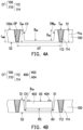
- FIG. 4 A to FIG. 4 G are schematic cross-sectional views illustrating a manufacturing process of a package structure in accordance with some alternative embodiments of the disclosure.
- FIG. 5 is a schematic cross-sectional view illustrating a package structure in accordance with some alternative embodiments of the disclosure.
- FIG. 6 A to FIG. 6 E are schematic cross-sectional views illustrating a manufacturing process of a carrier substrate in accordance with some alternative embodiments of the disclosure.
- FIG. 7 A to FIG. 7 D are schematic cross-sectional views illustrating various methods for placing the through carrier vias (TCV) in the openings of the insulating body of FIG. 6 B .
- TCV through carrier vias
- FIG. 8 A to FIG. 8 E are schematic cross-sectional views illustrating a manufacturing process of a carrier substrate in accordance with some alternative embodiments of the disclosure.
- FIG. 9 is a schematic cross-sectional view illustrating a package structure in accordance with some alternative embodiments of the disclosure.
- FIG. 10 is a schematic cross-sectional view illustrating a package structure in accordance with some alternative embodiments of the disclosure.
- FIG. 11 is a schematic cross-sectional view illustrating a package structure in accordance with some alternative embodiments of the disclosure.
- FIG. 12 A to FIG. 12 E are schematic cross-sectional views illustrating a manufacturing process of a carrier substrate in accordance with some alternative embodiments of the disclosure.
- FIG. 13 A to FIG. 13 F are schematic cross-sectional views illustrating a manufacturing process of a package structure in accordance with some alternative embodiments of the disclosure.
- FIG. 14 is a schematic cross-sectional view illustrating a package structure in accordance with some alternative embodiments of the disclosure.
- FIG. 15 is a schematic cross-sectional view illustrating a probe card in accordance with some alternative embodiments of the disclosure.
- first and second features are formed in direct contact
- additional features may be formed between the first and second features, such that the first and second features may not be in direct contact
- present disclosure may repeat reference numerals and/or letters in the various examples. This repetition is for the purpose of simplicity and clarity and does not in itself dictate a relationship between the various embodiments and/or configurations discussed.
- spatially relative terms such as “beneath,” “below,” “lower,” “above,” “upper” and the like, may be used herein for ease of description to describe one element or feature's relationship to another element(s) or feature(s) as illustrated in the figures.
- the spatially relative terms are intended to encompass different orientations of the device in use or operation in addition to the orientation depicted in the figures.
- the apparatus may be otherwise oriented (rotated 90 degrees or at other orientations) and the spatially relative descriptors used herein may likewise be interpreted accordingly.
- testing structures may be included to aid in the verification testing of the 3D packaging or 3DIC devices.
- the testing structures may include, for example, test pads formed in a redistribution layer or on a substrate that allows the testing of the 3D packaging or 3DIC, the use of probes and/or probe cards, and the like.
- the verification testing may be performed on intermediate structures as well as the final structure.
- the structures and methods disclosed herein may be used in conjunction with testing methodologies that incorporate intermediate verification of known good dies to increase the yield and decrease costs.
- FIG. 1 A to FIG. 1 E are schematic cross-sectional views illustrating a manufacturing process of a carrier substrate C 1 in accordance with some embodiments of the disclosure.
- an insulating body 100 is provided on a sacrificial film SF.
- the sacrificial film SF is made of organic materials.
- the sacrificial film SF is made of polymeric materials, such as acetal, acrylic, cellulose, acetate, polyethylene, polystyrene, vinyl, nylon, polyolefin, polyester, silicone, paraffin, or a combination thereof.
- the insulating body 100 is made of a dielectric material.
- the insulating body 100 is made of inorganic materials such as ceramics or glass.
- the insulating body 100 is made of aluminum nitride (AlN), aluminum oxide (Al 2 O 3 ), silicon nitride (Si 3 N 4 ), silicon carbide (SiC), or the like.
- the insulating body 100 is free of fillers.
- the insulating body 100 is an electrically insulating body. In other words, the insulating body 100 is not electrically conductive.
- the insulating body 100 is not thermal insulating. In other words, the insulating body 100 is thermally conductive.
- a Young's modulus of the insulating body 100 ranges from about 50 GPa to about 700 GPa.
- the Young's modulus of the insulating body 100 is respectively about 302 GPa to about 348 GPa, about 344 GPa to about 408 GPa, about 166 GPa to about 297 GPa, about 401 GPa to about 700 GPa, or about 50 GPa to about 90GPa.
- a hardness of the insulating body 100 ranges from about 5 Moh's to about 10 Moh's.
- a thermal expansion coefficient (CTE) of the insulating body 100 ranges from about 2.6 ppm/° C. to about 9.7 ppm/° C. In some embodiments, a thermal conductivity of the insulating body 100 ranges from about 0.96 W/m ⁇ K to about 350 W/m ⁇ K. In some embodiments, the insulating body 100 has a thickness t 100 ranging from about 50 ⁇ m to about 1000 ⁇ m. In some embodiments, the insulating body 100 has a first surface 100 a and a second surface 100 b opposite to the first surface 100 a . As illustrated in FIG. 1 A , the sacrificial film SF is attached to the second surface 100 b of the insulating body 100 .
- CTE thermal expansion coefficient
- the insulating body 100 has a plurality of openings OP formed therein.
- the openings OP may be formed by, for example, laser drilling, mechanical drilling, etching, or the like. As illustrated in FIG. 1 A , each opening OP extends from the first surface 100 a of the insulating body 100 to the second surface 100 b of the insulating body 100 . That is, each opening OP penetrates through the insulating body 100 .
- a depth D OP of each opening OP is substantially equal to the thickness t 100 of the insulating body 100 . In some embodiments, a depth D OP of each opening OP ranges from about 50 ⁇ m to about 1000 ⁇ m.
- the openings OP partially expose the sacrificial film SF.
- each opening OP has a slanted sidewall SW OP . That is, a first diameter DA OP of each opening OP at the first surface 100 a of the insulting body 100 is different from a second diameter DB OP of each opening OP at the second surface 100 b .
- the first diameter DA OP of each opening OP is larger than a second diameter DB OP of each opening OP.
- each opening OP may be in the form of a conical frustum.
- the disclosure is not limited thereto.
- each opening OP may have a substantially straight sidewall SW OP . That is, the first diameter DA OP of each opening OP may be substantially equal to the second diameter DB OP of each opening OP, and each opening OP may be in the form of a cylinder. In some embodiments, the first diameter DA OP ranges from about 20 ⁇ m to about 500 ⁇ m and the second diameter DB OP ranges from about 5 ⁇ m to about 500 ⁇ m. In some embodiments, two adjacent openings OP 2 are formed to have a pitch p 1 ranging from about 100 ⁇ m to about 1000 ⁇ m. It should be noted that throughout the entire disclosure, a pitch of two adjacent elements denotes a distance between centers of these two adjacent elements.
- a seed material layer 112 a is conformally formed on the insulating body 100 .
- the seed material layer 112 a is formed over the insulating body 100 and within the openings OP.
- the seed material layer 112 a covers the first surface 100 a of the insulating body 100 and extends into the openings OP to cover sidewalls SW OP of the openings OP.
- the seed material layer 112 a also covers the exposed portion of the sacrificial film SF. As illustrated in FIG. 1 B, the seed material layer 112 a is in physical contact with the insulating body 100 .
- the seed material layer 112 a may be formed through a sputtering process, a physical vapor deposition (PVD) process, or the like.
- the seed material layer 112 a is constituted by two sub-layers (not shown).
- the first sub-layer may include titanium, titanium nitride, tantalum, tantalum nitride, other suitable materials, or a combination thereof.
- the second sub-layer may include copper, copper alloys, or other suitable choice of materials.
- a conductive material layer 114 a is deposited onto the seed material layer 112 a .
- the conductive material layer 114 a is formed over the seed material layer 112 a located on top of the first surface 100 a of the insulating body 100 and over the seed material layer 112 a located within the openings OP.
- the conductive material layer 114 a is formed through a plating process.
- the plating process is, for example, an electro-plating process, an immersion plating process, or the like.
- the conductive material layer 114 a is made of aluminum, titanium, copper, nickel, tungsten, and/or alloys thereof.
- a portion of the seed material layer 112 a and a portion of the conductive material layer 114 a are removed to respectively form a seed layer 112 and a conductive layer 114 within each opening OP of the insulating body 100 .
- the portion of the seed material layer 112 a and the portion of the conductive material layer 114 a are removed until the first surface 100 a of the insulating body 100 is exposed.
- portions of the seed material layer 112 a and the conductive material layer 114 a that are above the first surface 100 a of the insulating body 100 are removed to form the seed layer 112 and the conductive layer 114 .
- the portion of the seed material layer 112 a and the portion of the conductive material layer 114 are removed through a planarization process, an etching process, or the like.
- the planarization process includes, for example, a chemical mechanical polishing (CMP) process, a mechanical grinding process, or the like.
- the etching process includes, for example, an anisotropic etching process such as dry etch or an isotropic etching process such as wet etch.
- the remaining seed layer 112 and the remaining conductive material layer 114 a within the same opening OP are collectively referred to as a through carrier vias (TCV) 110 . As illustrated in FIG. 1 D , multiple TCVs 110 are embedded within the insulating body 100 .
- the sacrificial film SF is removed to expose the second surface 100 b of the insulating body 100 , so as to obtain a carrier substrate C 1 .
- the sacrificial film SF is removed through an etching process, a stripping process, or the like.
- the carrier substrate C 1 includes the insulating body 100 and the TCVs 110 .
- the TCVs 110 are embedded in the insulating body 100 .
- the insulating body 100 laterally encapsulates the TCVs 110 .
- the geometry and the shape of the TCVs 110 are substantially the same as the openings OP of the insulating body 100 .
- a height H 110 of each TCV 110 is substantially the same as the depth D OP of each opening OP (shown in FIG. 1 A ).
- each TCV 110 penetrates through the insulating body 100 .
- the height H 110 of each TCV 110 is substantially equal to the thickness two of the insulating body 100 .
- the height H 110 of each TCV 110 ranges from about 50 ⁇ m to about 1000 ⁇ m.
- each TCV 110 has a slanted sidewall SW 110 . That is, a first diameter DA 110 of each TCV 110 is different from a second diameter DB 110 of each TCV 110 .
- the first diameter DA 110 of each TCV 110 is larger than a second diameter DB 110 of each TCV 110 .
- each TCV 110 may be in the form of a conical frustum.
- the disclosure is not limited thereto.
- the TCVs 110 may have a substantially straight sidewall SW 110 in some alternative embodiments.
- the first diameter DA 110 of each TCV 110 may be substantially equal to the second diameter DB 110 of each TCV 110 , and each TCV 110 may be in the form of a cylinder.
- the first diameter DA 110 ranges from about 20 ⁇ m to about 500 ⁇ m and the second diameter DB 110 ranges from about 5 ⁇ m to about 500 ⁇ m.
- two adjacent TCVs 110 are formed to have a pitch p 2 ranging from about 100 ⁇ m to about 1000 ⁇ m.
- each TCV 110 has a seed layer 112 and a conductive layer 114 surrounded by the seed layer 112 .
- the seed layer 112 is in physical contact with the insulating body 100 . That is, each TCV 110 is in physical contact with the insulating body 100 .
- top surfaces T 110 and bottom surfaces B 110 of the TCVs 110 are exposed by the insulating body 100 .
- the top surfaces T 110 of the TCVs 110 are substantially coplanar with the first surface 100 a of the insulating body 100 .
- the bottom surfaces B 110 of the TCVs 110 are substantially coplanar with the second surface 100 b of the insulating body 100 .
- the top surfaces T 110 of the TCVs 110 and the first surface 100 a of the insulating body 100 are collectively referred to as a first surface S 1 of the carrier substrate C 1 .
- the bottom surface B 110 of the TCVs 110 and the second surface 100 b of the insulating body 100 are collectively referred to as a second surface S 2 of the carrier substrate C 1 .
- the first surface S 1 of the carrier substrate C 1 is opposite to the second surface S 2 of the carrier substrate C 1 .
- the TCVs 110 are formed through an electro-plating process. As compared to the TCVs formed by electro-less plating process or conductive paste filling process, the TCVs 110 formed by the electro-plating process has higher electrical conductivity, higher throughput, as well as higher quality (i.e. free of voids within the TCVs 110 ). As such, the overall cost for manufacturing the carrier substrate C 1 may be effectively reduced and the quality of the carrier substrate C 1 may be ensured.
- FIG. 1 A to FIG. 1 E is one of the methods to manufacture the carrier substrate C 1 .
- Another way of manufacturing the carrier substrate C 1 will be described below in conjunction with FIG. 2 A to FIG. 2 E .
- FIG. 2 A to FIG. 2 E are schematic cross-sectional views illustrating a manufacturing process of a carrier substrate C 1 in accordance with some alternative embodiments of the disclosure.
- an insulating body 100 is provided.
- the insulating body in FIG. 2 A is similar to the insulating body 100 in FIG. 1 A , so the detailed description thereof is omitted herein.
- the openings OP do not penetrate through the insulating body 100 .
- the depth D OP of each opening OP is smaller than the thickness t 100 of the insulating body 100 .
- the sacrificial film in FIG. 1 A is omitted in FIG. 2 A .
- the second surface 100 b of the insulating body 100 is exposed in FIG. 2 A .
- FIG. 2 B to FIG. 2 D the steps illustrated in FIG. 2 B to FIG. 2 D are similar to the steps illustrated in FIG. 1 B to FIG. 1 D , so the detailed descriptions thereof are omitted herein.
- a portion of the insulating body 100 is removed to expose the bottom surfaces B 110 of the TCVs 110 , so as to obtain a carrier substrate C 1 .
- a planarization process or an etching process is performed on the insulating body 100 from the second surface 100 b shown in FIG. 2 D until the bottom surfaces B 110 of the TCVs 110 are revealed.
- the planarization process includes, for example, a CMP process, a mechanical grinding process, or the like.
- the etching process includes, for example, an anisotropic etching process such as dry etch or an isotropic etching process such as wet etch.
- the TCVs 110 may be slightly planarized or etched from the bottom surfaces B 110 thereof to further reduce the overall thickness of the carrier substrate C 1 . It should be noted that although FIG. 1 A to FIG. 1 E and FIG. 2 A to FIG. 2 E illustrated two different methods of manufacturing the carrier substrate C 1 , the structure of the carrier substrate C 1 obtained through these two methods may be substantially the same.
- the carrier substrate C 1 may be utilized in various application.
- the carrier substrate C 1 may be incorporate into various package structures to serve as a supporting mechanism which also provides electrical path.
- the applications of the carrier substrate C 1 will be described below in conjunction with FIG. 3 A to FIG. 3 G , FIG. 4 A to FIG. 4 G , and FIG. 5 .
- FIG. 3 A to FIG. 3 G are schematic cross-sectional views illustrating a manufacturing process of a package structure 10 in accordance with some alternative embodiments of the disclosure.
- the carrier substrate C 1 in FIG. 1 E and FIG. 2 E is provided.
- a plurality of routing patterns 200 is formed on the first surface S 1 of the insulating body 100 .
- the routing patterns 200 are formed to be in physical contact with the top surface T 110 of the TCVs 110 to render electrical connection with the TCVs 110 .
- the routing patterns 200 are formed through a plating process followed by an etching process.
- the plating process includes, for example, an electro-plating process, an electro-less plating process, an immersion plating process, or the like.
- the etching process includes, for example, an anisotropic etching process such as dry etch or an isotropic etching process such as wet etch.
- the routing patterns 200 includes copper, nickel, titanium, a combination thereof, or the like.
- a plurality of through insulating vias (TIV) 300 is formed over the routing patterns 200 .
- the TIVs 300 are formed by the following steps. First, a seed material layer (not shown) is conformally formed over the routing patterns 200 and the first surface S 1 of the carrier substrate C 1 .
- the seed material layer includes a titanium/copper composite layer, and is formed by a sputtering process. Thereafter, a photoresist layer (not shown) with openings is formed on the seed material layer, and the openings of the photoresist layer expose the intended locations for the subsequently formed TIVs 300 .
- a plating process is performed to form a metal material layer (e.g., a copper layer) on the seed material layer exposed by the openings of the photoresist layer.
- a plating process is performed to form a metal material layer (e.g., a copper layer) on the seed material layer exposed by the openings of the photoresist layer.
- the photoresist layer and the underlying seed material layer are then removed to form the TIVs 300 .
- a die 400 is disposed over the first surface S 1 of the carrier substrate C 1 .
- the die 400 is disposed through a pick-and-place process or the like.
- the die 400 is attached to the first surface S 1 of the carrier substrate C 1 through an adhesive layer AD.
- the adhesive layer AD is sandwiched between the die 400 and the first surface S 1 of the carrier substrate C 1 to fix the die 400 in place.
- the adhesive layer AD covers some of the routing patterns 200 . In other words, some of the routing patterns 200 are located directly underneath the die 400 .
- the adhesive layer AD includes die attach film (DAF) or the like.
- each die 400 includes a semiconductor substrate 402 and a plurality of conductive posts 404 .
- the semiconductor substrate 402 is made of silicon or germanium. However, the disclosure is not limited thereto.
- the semiconductor substrate 402 may also include other suitable semiconductor materials, such as elements in Group III, Group IV, and/or Group V in the periodic table.
- the conductive posts 404 are disposed over the semiconductor substrate 402 .
- the conductive posts 404 protrude from the semiconductor substrate 402 .
- the conductive posts 404 may be copper posts or other suitable metallic posts.
- the die 400 further includes an interconnection structure (not shown) and a plurality of conductive pads (not shown) embedded in the semiconductor substrate 402 or located between the conductive posts 404 and the semiconductor substrate 402 .
- the die 400 has an active surface AS and a rear surface RS opposite to the active surface AS. As illustrated in FIG. 3 B , the rear surface RS of the die 400 is attached to the adhesive layer AD while the active surface AS of the die 400 faces upward. In some embodiments, the active surface AS of the die 400 is exposed to atmospheric environment.
- the TIVs 300 are formed prior to the placement of the die 400 .
- the disclosure is not limited thereto.
- the die 400 may be placed prior to the formation of the TIVs 300 .
- an encapsulant 500 is formed over the first surface S 1 of the carrier substrate C 1 to laterally encapsulate the TIVs 300 and the die 400 .
- the encapsulant 500 includes a molding compound, a molding underfill, a resin (such as epoxy), or the like.
- the encapsulant 500 includes a photo-sensitive material such as polybenzoxazole (PBO), polyimide (PI), benzocyclobutene (BCB), a combination thereof, or the like.
- the encapsulant 500 includes fillers. The fillers may be particles made of silica, aluminum dioxide, or the like.
- the encapsulant 500 is formed by the following steps.
- an insulating material (not shown) is formed on the routing patterns 200 and the first surface S 1 of the carrier substrate C 1 through a molding process, so as to encapsulate the TIVs 300 and the die 400 .
- the molding process includes, for example, a transfer molding process, a compression molding process, or the like.
- the conductive posts 404 are encapsulated by the insulating material. In other words, the conductive posts 404 are not revealed and are well protected by the insulating material.
- the insulating material is grinded until top surfaces of the TIVs 300 and top surfaces of the conductive posts 404 are exposed, so as to form the encapsulant 500 .
- the insulating material is grinded by a mechanical grinding process and/or a CMP process.
- portions of the TIVs 300 and portions of the conductive posts 404 are also slightly grinded. As illustrated in FIG. 3 C , after the grinding process, the TIVs 300 penetrate through the encapsulant 500 .
- a redistribution structure 600 is formed over the TIVs 300 , the die 400 , and the encapsulant 500 .
- the redistribution structure 600 includes a plurality of conductive patterns 602 , a plurality of conductive vias 604 , and a dielectric layer 606 .
- the conductive patterns 602 and the conductive vias 604 are formed through a plating process followed by an etching process.
- the plating process includes, for example, an electro-plating process, an electro-less plating process, an immersion plating process, or the like.
- the etching process includes, for example, an anisotropic etching process such as dry etch or an isotropic etching process such as wet etch.
- the conductive patterns 602 and the underlying conductive vias 604 are simultaneously formed.
- a material of the conductive patterns 602 and the conductive vias 604 includes aluminum, titanium, copper, nickel, tungsten, and/or alloys thereof.
- the dielectric layer 606 encapsulates the conductive patterns 602 and the conductive vias 604 .
- the dielectric layer 606 is a polymer layer made of PBO, PI, BCB, a combination thereof, or the like.
- the dielectric layer 606 is illustrated as a bulky layer in FIG. 3 D , but it should be understood that the dielectric layer 606 may be constituted by multiple dielectric layers.
- the conductive vias 604 are in physical contact with the TIVs 300 and the conductive posts 404 of the die 400 .
- the conductive vias 604 render electrical connection between the redistribution structure 600 and the TIVs 300 and between the redistribution structure 600 and the die 400 .
- the die 400 is electrically connected to the TCVs 110 of the carrier substrate C 1 sequentially through the redistribution structure 600 , the TIVs 300 , and the routing patterns 200 .
- the structure illustrated in FIG. 3 D is flipped upside down such that the second surface S 2 of the carrier substrate C 1 faces upward. Thereafter, a redistribution structure 700 is formed on the second surface S 2 of the carrier substrate C 1 .
- the redistribution structure 700 includes a plurality of conductive patterns 702 , a plurality of conductive vias 704 , and a dielectric layer 706 .
- the conductive patterns 702 , the conductive vias 704 , and the dielectric layer 706 of the redistribution structure 700 are respectively similar to the conductive patterns 602 , the conductive vias 604 , and the dielectric layer 606 of the redistribution structure 600 , so the detailed descriptions thereof are omitted herein.
- the dielectric layer 706 is illustrated as a bulky layer in FIG. 3 E , but it should be understood that the dielectric layer 706 may be constituted by multiple dielectric layers.
- the conductive patterns 702 and the dielectric layers of the dielectric layer 706 are stacked alternately. In some embodiments, two adjacent conductive patterns 702 in the vertical direction are electrically connected to each other through the conductive vias 704 sandwiched therebetween.
- the bottommost conductive patterns 702 are in physical contact with the bottom surface B 110 of the TCVs 110 .
- the redistribution structure 700 is electrically connected to the TCVs 110 through the bottommost conductive patterns 702 .
- the dielectric layer 706 exposes the topmost conductive patterns 702 .
- FIG. 3 A to FIG. 3 E illustrated that the routing patterns 200 , the TIVs 300 , the die 400 , the encapsulant 500 , and the redistribution structure 600 are formed on the carrier substrate C 1 prior to the formation of the redistribution structure 700 , the disclosure is not limited thereto.
- the redistribution structure 700 may be formed on the carrier substrate C 1 prior to the routing patterns 200 , the TIVs 300 , the die 400 , the encapsulant 500 , and the redistribution structure 600 .
- a plurality of conductive terminals 800 is formed on the redistribution structure 700 .
- the conductive terminals 800 are formed on the topmost conductive patterns 702 exposed by the dielectric layer 706 .
- the conductive terminals 800 are solder balls, ball grid array (BGA) balls, or the like.
- the conductive terminals 800 are made of a conductive material with low resistivity, such as Sn, Pb, Ag, Cu, Ni, Bi, or an alloy thereof.
- the structure illustrated in FIG. 3 F is flipped upside down and a singulation process is performed on the structure to obtain a package structure 10 .
- the singulation process typically involves dicing with a rotation blade and/or a laser beam.
- the singulation process includes a laser cutting process, a mechanical cutting process, a laser grooving process, other suitable processes, or a combination thereof.
- FIG. 4 A to FIG. 4 G are schematic cross-sectional views illustrating a manufacturing process of a package structure 20 in accordance with some alternative embodiments of the disclosure.
- a carrier substrate C 1 ′ is provided.
- the carrier substrate C 1 ′ in FIG. 4 A is similar to the carrier substrate C 1 in FIG. 1 E and FIG. 2 E , so the detailed description thereof is omitted herein.
- the difference between the carrier substrate C 1 ′ in FIG. 4 A and the carrier substrate C 1 in FIG. 1 E and FIG. 2 E is that a pitch p 2 between two adjacent TCVs 110 in the carrier substrate C 1 ′ of FIG. 4 A is larger than the pitch p 2 between two adjacent TCVs 110 in the carrier substrate C 1 of FIG.
- a cavity CV is formed in the insulating body 100 .
- the insulating body 100 of the carrier substrate C 1 ′ has the cavity CV.
- the cavity CV is formed by laser drilling, mechanical drilling, etching, or the like.
- the cavity CV is formed between adjacent TCVs 110 .
- the cavity CV is surrounded by the TCVs 110 .
- a depth D CV of the cavity CV is smaller than a depth D OP of each opening OP.
- the depth D CV of the cavity CV is also smaller than the height H 110 of each TCV 110 . That is, the cavity CV does not penetrate through the insulating body 100 .
- the depth D CV of the cavity CV ranges from about 50 ⁇ m to about 750 ⁇ m.
- sidewalls SW CV of the cavity CV are slanted.
- the first surface 100 a of the insulating body 100 , the top surface T 110 of the TCVs 110 , the sidewalls SW CV of the cavity CV, and a bottom surface B CV of the cavity CV are collectively referred to as the first surface S 1 of the carrier substrate C 1 ′.
- a die 400 is disposed within the cavity CV.
- the die 400 in FIG. 4 B is similar to the die 400 in FIG. 3 B , so the detailed description thereof is omitted herein.
- the die 400 is placed such that the active surface AS of the die 400 faces upward.
- the rear surface RS of the die 400 is attached to the bottom surface B CV of the cavity CV through an adhesive layer AD.
- the bottom surface B CV is being considered as part of the first surface S 1 of the carrier substrate C 1 ′, so the die 400 is being considered as disposed over the first surface S 1 of the carrier substrate C 1 ′.
- the adhesive layer AD includes DAF or the like.
- an encapsulant 500 is formed in the cavity CV to laterally encapsulate the die 400 . That is, the die 400 and the encapsulant 500 are both located within the cavity CV, and at least a portion of the encapsulant 500 is sandwiched between the die 400 and the insulating body 100 .
- the encapsulant 500 in FIG. 4 C is similar to the encapsulant 500 in FIG. 3 C , so the detailed description thereof is omitted herein.
- the encapsulant 500 exposes top surfaces of the conductive posts 404 of the die 400 for future electrical connection.
- a redistribution structure 600 is formed on the insulating body 100 , the TCVs 110 , the die 400 , and the encapsulant 500 .
- the redistribution structure 600 includes a plurality of conductive patterns 602 , a plurality of conductive vias 604 , and a dielectric layer 606 .
- the conductive patterns 602 , the conductive vias 604 , and the dielectric layer 606 in FIG. 4 D are respectively similar to the conductive patterns 602 , the conductive vias 604 , and the dielectric layer 606 in FIG. 3 D , so the detailed descriptions thereof are omitted herein. As illustrated in FIG.
- the conductive vias 604 are in physical contact with the TCVs 110 and the conductive posts 404 of the die 400 .
- the conductive vias 604 render electrical connection between the redistribution structure 600 and the TCVs 110 and between the redistribution structure 600 and the die 400 .
- the die 400 is electrically connected to the TCVs 110 of the carrier substrate C 1 ′ through the redistribution structure 600 .
- the structure illustrated in FIG. 4 D is flipped upside down such that the second surface S 2 of the carrier substrate C 1 ′ faces upward. Thereafter, a redistribution structure 700 is formed on the second surface S 2 of the carrier substrate C 1 ′.
- the redistribution structure 700 includes a plurality of conductive patterns 702 , a plurality of conductive vias 704 , and a dielectric layer 706 .
- the conductive patterns 702 , the conductive vias 704 , and the dielectric layer 706 in FIG. 4 E are respectively similar to the conductive patterns 702 , the conductive vias 704 , and the dielectric layer 706 in FIG. 3 E , so the detailed descriptions thereof are omitted herein.
- a plurality of conductive terminals 800 is formed on the redistribution structure 700 .
- the conductive terminals 800 in FIG. 4 F are similar to the conductive terminals 800 in FIG. 3 F , so the detailed descriptions thereof are omitted herein.
- the structure illustrated in FIG. 4 F is flipped upside down and a singulation process is performed on the structure to obtain a package structure 20 .
- the singulation process typically involves dicing with a rotation blade and/or a laser beam.
- the singulation process includes a laser cutting process, a mechanical cutting process, a laser grooving process, other suitable processes, or a combination thereof.
- FIG. 5 is a schematic cross-sectional view illustrating a package structure 30 in accordance with some alternative embodiments of the disclosure.
- the package structure 30 includes a carrier substrate C 1 , a plurality of routing patterns 200 , a die 400 , a redistribution structure 700 , a plurality of connectors 900 , and an underfill layer 1000 .
- the carrier substrate C 1 , the routing patterns 200 , the die 400 , and the redistribution structure 700 in FIG. 5 are respectively similar to the carrier substrate C 1 , the routing patterns 200 , the die 400 , and the redistribution structure 700 in FIG. 3 G , so the detailed descriptions thereof are omitted herein.
- the die 400 is disposed over the first surface S 1 of the carrier substrate C 1 .
- the die 400 is placed in a face down manner. In other words, the die 400 is placed such that the active surface AS of the die 400 faces downward.
- the die 400 is bonded to the routing patterns 200 through flip-chip bonding.
- the conductive posts 404 of the die 400 are attached to the routing patterns 200 through the connectors 900 .
- the connectors 900 are made of a conductive material with low resistivity, such as Sn, Pb, Ag, Cu, Ni, Bi, or an alloy thereof.
- the underfill layer 1000 laterally encapsulates the routing patterns 200 , the conductive posts 404 of the die 400 , and the connectors 900 to protect these elements. In some embodiments, the underfill layer 1000 further covers a portion of each sidewall of the semiconductor substrate 402 of the die 400 .
- a material of the underfill layer 1000 is an insulating material and may include a resin (e.g., epoxy resin), a filler material, a stress release agent (SRA), an adhesion promoter, other material, or a combination thereof. In some embodiments, the underfill layer 1000 is optional.
- the redistribution structure 700 and the conductive terminals 800 are sequentially disposed over the second surface S 2 of the carrier substrate C 1 .
- the TCVs 110 allow electrical connection between the die 400 over the first surface S 1 of the carrier substrate C 1 and the redistribution structure 700 over the second surface S 2 of the carrier substrate C 1 .
- FIG. 6 A to FIG. 6 E are schematic cross-sectional views illustrating a manufacturing process of a carrier substrate C 2 in accordance with some alternative embodiments of the disclosure.
- an insulating body 100 is provided on a sacrificial film SF.
- the insulating body 100 and the sacrificial film SF in FIG. 6 A are respectively similar to the insulating body 100 and the sacrificial film SF in FIG. 1 A , so the detailed descriptions thereof are omitted herein.
- a plurality of TCVs 110 a is formed in the openings OP of the insulating body 100 .
- the TCVs 110 a are pre-fabricated and are placed into the openings OP of the insulating body 100 .
- the TCVs 110 a are pre-fabricated conductive posts or conductive pillars.
- the TCVs 110 a are placed to be standing on the sacrificial film SF.
- the pre-fabricated TCVs 110 a may be placed into the openings OP through various processes. These processes will be described below in conjunction with FIG. 7 A to FIG. 7 D .
- FIG. 7 A to FIG. 7 D are schematic cross-sectional views illustrating various methods for placing the TCVs 110 a in the openings OP of the insulating body 100 of FIG. 6 B .
- a stencil ST is provided over the insulating body 100 .
- the stencil ST has a plurality of apertures AP, and each aperture AP exposes the corresponding opening OP of the insulating body 100 .
- a plurality of pre-fabricated TCVs 110 a is placed over the stencil ST.
- a scraper SC is provided over the stencil ST and the TCVs 110 a .
- the scraper SC moves along the span of the insulating body 100 and scrapes the TCVs 110 a above the stencil ST into the apertures AP of the stencil ST and the openings OP of the insulating body 100 during the movement thereof.
- the TCVs 110 a are able to roll on an upper surface of the stencil ST, and the scraper SC may easily drive the TCVs 110 a into the apertures AP of the stencil ST and the openings OP of the insulating body 100 .
- a stencil ST is provided over the insulating body 100 .
- the stencil ST has a plurality of apertures AP, and each aperture AP exposes the corresponding opening OP of the insulating body 100 .
- a plurality of pre-fabricated TCVs 110 a is placed over the stencil ST. Thereafter, the insulating body 100 is tilted, so the TCVs 110 a are driven into the apertures AP of the stencil ST and the openings OP of the insulating body 100 by gravitational force.
- the TCVs 110 a are able to roll on an upper surface of the stencil ST, and the gravitational force causes the TCVs 110 a to fall into the apertures AP of the stencil ST and the openings OP of the insulating body 100 .
- the insulating body 100 is vibrated while being tilted.
- the TCVs 110 a are subjected to a specific vibration frequency to further aid the rolling of the TCVs 110 a.
- a stencil ST is provided over the insulating body 100 .
- the stencil ST has a plurality of apertures AP, and each aperture AP exposes the corresponding opening OP of the insulating body 100 .
- a plurality of pre-fabricated TCVs 110 a is placed over the stencil ST.
- a suction mechanism (not shown) above the stencil ST and the TCVs 110 a is turned on to suck the TCVs 110 a upward.
- the suction mechanism is turned off so the TCVs 110 a would drop into the apertures AP of the stencil ST and the openings OP of the insulating body 100 due to the gravitational force.
- the foregoing process may be repeated multiple times until each opening OP accommodates one TCV 110 a.
- the TCVs 110 a are placed into the openings OP of the insulating body 100 through a picked-and-placed process.
- the pre-fabricated TCVs 110 a are being picked up by a placing tool TL one by one, and are being placed into the openings OP of the insulating body 100 through the placing tool TL one by one.
- the processes of placing the TCVs 110 a into the openings OP of the insulating body 100 in FIG. 7 A to FIG. 7 D are illustrated as individual processes, the disclosure is not limited thereto. In some alternative embodiments, at least two of the processes respectively shown in FIG. 7 A to FIG. 7 D may be combined to place the TCVs 110 a into the openings OP of the insulating body 100 .
- a height H 110a of each TCV 110 a is substantially the same as the depth D OP of each opening OP.
- the height H 110a of each TCV 110 a ranges from about 50 ⁇ m to about 1000 ⁇ m.
- each TCV 110 a has a substantially straight sidewall SW 110a . That is, a first diameter DA 110a of each TCV 110 a may be substantially equal to a second diameter DB 110a of each TCV 110 a , and each TCV 110 a may be in the form of a cylinder. As illustrated in FIG. 6 B , the first diameter DA 110a of each TCV 110 a is smaller than the first diameter DA OP of each opening OP.
- first diameter DA 110a and the second diameter DB 110a of each TCV 110 a are substantially equal to the second diameter DB OP of each opening OP.
- both of the first diameter DA 110a and the second diameter DB 110a of each TCV 110 a is smaller than the first diameter DA OP and the second diameter DB OP of each opening OP.
- the first diameter DA 110a and the second diameter DB 110a range from about 50 ⁇ m to about 300 ⁇ m.
- two adjacent TCVs 110 a are formed to have a pitch p 2 ranging from about 100 ⁇ m to about 1000 ⁇ m.
- a filling material layer 120 a is formed over the insulating body 100 .
- the filling material layer 120 a covers the first surface 100 a of the insulating body 100 and fills into the openings OP of the insulating body 100 .
- the TCVs 110 a located in the openings OP of the insulating body 100 are encapsulated by the filling material layer 120 a .
- the filling material layer 120 a is made of organic materials.
- the filling material layer 120 a is made of polymeric materials, such as acetal, acrylic, cellulose, acetate, polyethylene, polystyrene, vinyl, nylon, polyolefin, polyester, silicone, paraffin, or a combination thereof.
- the filling material layer 120 a is made of a molding compound.
- the filling material layer 120 a may further include fillers.
- the fillers may be particles made of silica, aluminum dioxide, or the like.
- the filling material layer 120 a is formed through atomic layer deposition (ALD), chemical vapor deposition (CVD), plasma enhanced chemical vapor deposition (PECVD), high density plasma chemical vapor deposition (HDPCVD), physical vapor deposition (PVD), or the like.
- the filling material layer 120 a may be formed through a transfer molding process, a compression molding process, or any other suitable molding processes.
- a Young's modulus of the filling material layer 120 a ranges from about 3 GPa to about 30 GPa.
- the Young's modulus thereof ranges from about 3 GPa to about 5 GPa.
- the filling material layer 120 a is made of a molding compound
- the Young's modulus thereof ranges from about 15 GPa to about 30 GPa.
- a portion of the filling material layer 120 a is removed to form a plurality of filling patterns 120 in the openings OP of the insulating body 100 .
- the portion of the filling material layer 120 a is removed until the top surfaces T 110a of the TCVs 110 a are exposed.
- the filling material layer 120 a above the first surface 100 a of the insulating body 100 is removed to form the filling patterns 120 .
- the portion of the filling material layer 120 a is removed through a planarization process, an etching process, or the like.
- the planarization process includes, for example, a CMP process, a mechanical grinding process, or the like.
- the etching process includes, for example, an anisotropic etching process such as dry etch or an isotropic etching process such as wet etch.
- the filling patterns 120 are sandwiched between each TCV 110 a and the insulating body 100 .
- the sacrificial film SF is removed to expose the second surface 100 b of the insulating body 100 , so as to obtain a carrier substrate C 2 .
- the sacrificial film SF is removed through an etching process, a stripping process, or the like.
- the carrier substrate C 2 includes the insulating body 100 , the TCVs 110 a , and the filling patterns 120 .
- the TCVs 110 a are embedded in the insulating body 100 and the filling patterns 120 .
- each filling pattern 120 laterally encapsulates the corresponding TCV 110 a
- the insulating body 100 laterally encapsulates the filling patterns 120 .
- the insulating body 100 and the filling patterns 120 are made of different materials. As illustrated in FIG. 6 E , each TCV 110 a and each filling pattern 120 penetrate through the insulating body 100 . In other words, the height H 110a of each TCV 110 a and a height H 120 of each filling pattern 120 are substantially equal to the thickness t 100 of the insulating body 100 . For example, the height H 110a of each TCV 110 a and the height H 120 of each filling pattern 120 range from about 50 ⁇ m to about 1000 ⁇ m.
- each filling pattern 120 is sandwiched between each TCV 110 a and the insulating body 100 .
- the filling patterns 120 are in physical contact with the insulating body 100 and the TCVs 110 a .
- the geometry and the shape of the filling patterns 120 depend on the geometries and the shapes of the openings OP and the TCVs 110 a .
- an inner sidewall ISW 120 of each filling pattern 120 follows a profile of the sidewall SW 110a of the corresponding TCV 110 a in which the filling pattern 120 is in physical contact with.
- each filling pattern 120 follows a profile of the sidewall SW OP of the corresponding opening OP of the insulating body 100 .
- each filling pattern 120 has an inner sidewall ISW 120 contacting the corresponding TCV 110 a and an outer sidewall OSW 120 contacting the insulating body 100 .
- each TCV 110 a has a substantially straight sidewall SW 110a . Since the inner sidewall ISW 120 of the filling pattern 120 follows the profile of the sidewall SW 110a of the TCV 110 a , the inner sidewall ISW 120 of each filling pattern 120 is also substantially straight.
- each opening OP of the insulating body 100 has a slanted sidewall SW OP . Since the outer sidewall OSW 120 of the filling pattern 120 follows the profile of the sidewall SW OP of the openings, the outer sidewall OSW 120 of each filling pattern 120 is slanted.
- a Young's modulus of the filling patterns 120 ranges from about 3 GPa to about 30 GPa. For example, when the filling patterns 120 is made of a polymeric material, the Young's modulus thereof ranges from about 3 GPa to about 5 GPa. Alternatively, when the filling patterns 120 is made of a molding compound, the Young's modulus thereof ranges from about 15 GPa to about 30 GPa.
- top surfaces T 110a of the TCVs 110 a and top surfaces T 120 of the filling patterns 120 are substantially coplanar with the first surface 100 a of the insulating body 100 .
- bottom surfaces B 110 of the TCVs 110 are substantially coplanar with the second surface 100 b of the insulating body 100 .
- the top surfaces T 110 of the TCVs 110 , the top surfaces T 120 of the filling patterns 120 , and the first surface 100 a of the insulating body 100 are collectively referred to as a first surface S 1 of the carrier substrate C 2 .
- the bottom surface B 110 of the TCVs 110 and the second surface 100 b of the insulating body 100 are collectively referred to as a second surface S 2 of the carrier substrate C 2 .
- the second diameter DB 110a of each TCV 110 a is substantially equal to the second diameter DB OP of each opening OP of the insulating body 100 .
- the filling patterns 120 are not exposed at the second surface 100 b of the insulating body 100 (i.e. not exposed at the second surface S 2 of the carrier substrate C 2 ).
- the disclosure is not limited thereto.
- the second diameter DB 110a of the TCV 110 a is smaller than the second diameter DB OP of the opening OP of the insulating body 100 , bottom surfaces of the filling patterns 120 would be exposed at the second surface 100 b of the insulating body 100 .
- the bottom surface of the filling patterns 120 may be included as part of the second surface S 2 of the carrier substrate C 2 .
- the first surface S 1 of the carrier substrate C 2 is opposite to the second surface S 2 of the carrier substrate C 2 .
- the TCVs 110 a are pre-fabricated and are placed in the openings OP of the insulating body 100 .
- the pre-fabricated TCVs 110 a are able to achieve higher electrical conductivity, higher throughput, as well as higher quality (i.e. free of voids within the TCVs 110 ). As such, the overall cost for manufacturing the carrier substrate C 2 may be effectively reduced and the quality of the carrier substrate C 2 may be ensured.
- FIG. 8 A to FIG. 8 E are schematic cross-sectional views illustrating a manufacturing process of a carrier substrate C 2 in accordance with some alternative embodiments of the disclosure.
- an insulating body 100 is provided.
- the insulating body 100 in FIG. 8 A is similar to the insulating body 100 in FIG. 6 A , so the detailed description thereof is omitted herein.
- the openings OP do not penetrate through the insulating body 100 .
- the depth D OP of each opening OP is smaller than the thickness t 100 of the insulating body 100 .
- the sacrificial film in FIG. 6 A is omitted in FIG. 8 A .
- the second surface 100 b of the insulating body 100 is exposed in FIG. 8 A .
- FIG. 8 B to FIG. 8 D the steps illustrated in FIG. 8 B to FIG. 8 D are similar to the steps illustrated in FIG. 6 B to FIG. 6 D , so the detailed descriptions thereof are omitted herein.
- a portion of the insulating body 100 is removed to expose the bottom surfaces B 110a of the TCVs 110 a , so as to obtain a carrier substrate C 2 .
- a planarization process or an etching process is performed on the insulating body 100 from the second surface 100 b shown in FIG. 8 D until the bottom surfaces B 110a of the TCVs 110 a are exposed.
- the planarization process includes, for example, a CMP process, a mechanical grinding process, or the like.
- the etching process includes, for example, an anisotropic etching process such as dry etch or an isotropic etching process such as wet etch.
- the TCVs 110 a may be slightly planarized or etched from the bottom surfaces B 110a thereof to further reduce the overall thickness of the carrier substrate C 2 . It should be noted that although FIG. 6 A to FIG. 6 E and FIG. 8 A to FIG. 8 E illustrated two different methods of manufacturing the carrier substrate C 2 , the structure of the carrier substrate C 2 obtained through these two methods may be substantially the same.
- the carrier substrate C 2 may be utilized in various application.
- the carrier substrate C 2 may be incorporate into various package structures to serve as a supporting mechanism which also provides electrical path. The applications of the carrier substrate C 2 will be described below in conjunction with FIG. 9 to FIG. 11 .
- FIG. 9 is a schematic cross-sectional view illustrating a package structure 40 in accordance with some alternative embodiments of the disclosure.
- the package structure 40 in FIG. 9 is similar to the package structure 10 in FIG. 3 G , so similar elements are denoted by the same reference numeral, and the detailed descriptions thereof are omitted herein.
- the difference between the package structure 40 of FIG. 9 and the package structure 10 in FIG. 3 G lies in that the carrier substrate C 1 in FIG. 3 G is replaced by the carrier substrate C 2 in FIG. 9 . That is, the carrier substrate C 2 in FIG. 6 E and FIG. 8 E is incorporated into the package structure 40 of FIG. 9 .
- FIG. 9 As illustrated in FIG.
- the TCVs 110 a and the filling patterns 120 of the carrier substrate C 2 are in physical contact with the routing patterns 200 .
- the TCVs 110 a are well protected by the filling patterns 120 and are able to render electrical connection between the first surface S 1 and the second surface S 2 of the carrier substrate C 2 (i.e. between the die 400 and the redistribution structure 700 and between the TIVs 300 and the redistribution structure 700 ).
- FIG. 10 is a schematic cross-sectional view illustrating a package structure 50 in accordance with some alternative embodiments of the disclosure.
- the package structure 50 in FIG. 10 is similar to the package structure 20 in FIG. 4 G , so similar elements are denoted by the same reference numeral, and the detailed descriptions thereof are omitted herein.
- the difference between the package structure 50 of FIG. 10 and the package structure 20 in FIG. 4 G lies in that the carrier substrate C 1 ′ in FIG. 4 G is replaced by the carrier substrate C 2 ′ in FIG. 10 .
- the carrier substrate C 2 ′ in FIG. 10 is similar to the carrier substrate C 2 in FIG. 6 E and FIG. 8 E , so the detailed description thereof is omitted herein.
- the difference between the carrier substrate C 2 ′ in FIG. 10 and the carrier substrate C 2 in FIG. 6 E and FIG. 8 E is that a pitch p 2 between two adjacent TCVs 110 a in the carrier substrate C 2 ′ of FIG. 10 is larger than the pitch p 2 between two adjacent TCVs 110 a in the carrier substrate C 2 of FIG. 6 E and FIG. 8 E .
- a cavity CV is formed in the insulating body 100 .
- the filling patterns 120 of the carrier substrate C 2 ′ are in physical contact with the redistribution structure 600 .
- the filling patterns 120 of the carrier substrate C 2 ′ are in physical contact with the dielectric layer 606 of the redistribution structure 600 .
- the TCVs 110 a are well protected by the filling patterns 120 and are able to render electrical connection between the first surface S 1 and the second surface S 2 of the carrier substrate C 2 ′ (i.e. between the die 400 and the redistribution structure 700 ).
- FIG. 11 is a schematic cross-sectional view illustrating a package structure 60 in accordance with some alternative embodiments of the disclosure.
- the package structure 60 in FIG. 11 is similar to the package structure 30 in FIG. 5 , so similar elements are denoted by the same reference numeral, and the detailed descriptions thereof are omitted herein.
- the difference between the package structure 60 of FIG. 11 and the package structure 30 in FIG. 5 lies in that the carrier substrate C 1 in FIG. 5 is replaced by the carrier substrate C 2 in FIG. 11 . That is, the carrier substrate C 2 in FIG. 6 E and FIG. 8 E is incorporated into the package structure 60 of FIG. 11 .
- FIG. 11 As illustrated in FIG.
- the TCVs 110 a and the filling patterns 120 of the carrier substrate C 2 are in physical contact with the routing patterns 200 .
- the TCVs 110 a are well protected by the filling patterns 120 and are able to render electrical connection between the first surface S 1 and the second surface S 2 of the carrier substrate C 2 (i.e. between the die 400 and the redistribution structure 700 ).
- FIG. 12 A to FIG. 12 E are schematic cross-sectional views illustrating a manufacturing process of a carrier substrate C 3 in accordance with some alternative embodiments of the disclosure.
- an insulating body 100 is provided on a sacrificial film SF.
- the insulating body 100 and the sacrificial film SF in FIG. 12 A are respectively similar to the insulating body 100 and the sacrificial film SF in FIG. 6 A , so the detailed descriptions thereof are omitted herein.
- a pitch p 3 between two adjacent openings OP is larger than the pitch p 1 between two adjacent openings OP in FIG. 6 A .
- a plurality of TCVs 110 b is formed in the openings OP of the insulating body 100 .
- the formation method and the material of the TCVs 110 b in FIG. 12 B are similar to that of the TCVs 110 a in FIG. 6 B , so the detailed descriptions thereof are omitted herein.
- a height H 110b of each TCV 110 b is larger than the depth D OP of each opening OP. That is, each TCV 110 b is partially located in the corresponding opening OP and protrudes from the openings OP of the insulating body 100 . For example, each TCV 110 b protrudes above the first surface 100 a of the insulating body 100 .
- each TCV 110 b ranges from about 100 ⁇ m to about 1000 ⁇ m.
- each TCV 110 b has a substantially straight sidewall SW 110b . That is, a first diameter DA 110b of each TCV 110 b may be substantially equal to a second diameter DB 110b of each TCV 110 b , and each TCV 110 b may be in the form of a cylinder. As illustrated in FIG. 12 B , the first diameter DA 110b of each TCV 110 b is smaller than the first diameter DA OP of each opening OP.
- first diameter DA 110b and the second diameter DB 110b of each TCV 110 b are substantially equal to the second diameter DB OP of each opening OP.
- both of the first diameter DA 110b and the second diameter DB 110b of each TCV 110 b is smaller than the first diameter DA OP and the second diameter DB OP of each opening OP.
- the first diameter DA 110b and the second diameter DB 110b range from about 50 ⁇ m to about 300 ⁇ m. That is, an aspect ratio (i.e. a ratio of the height H 110b and the first diameter DA 110b /the second diameter DB 110b ) ranges from about 1 to about 10.
- a pitch p 4 between two adjacent TCVs 110 b is substantially equal to the pitch p 3 between two adjacent openings OP (shown in FIG. 12 A ).
- a filling material layer 120 a is formed over the insulating body 100 .
- the formation method and the material of the filling material layer 120 a in FIG. 12 C are similar to that of the filling material layer 120 a in FIG. 6 C , so the detailed descriptions thereof are omitted herein.
- the filling material layer 120 a covers the first surface 100 a of the insulating body 100 and fills into the openings OP of the insulating body 100 .
- the TCVs 110 b are laterally encapsulated by the filling material layer 120 a.
- a portion of the filling material layer 120 a is removed to form a plurality of filling patterns 120 in the openings OP of the insulating body 100 .
- the portion of the filling material layer 120 a is removed until the first surface 100 a of the insulating body 100 is exposed.
- the filling material layer 120 a above the first surface 100 a of the insulating body 100 is removed to form the filling patterns 120 .
- the portion of the filling material layer 120 a is removed through a planarization process, an etching process, or the like.
- the planarization process includes, for example, a CMP process, a mechanical grinding process, or the like.
- the etching process includes, for example, an anisotropic etching process such as dry etch or an isotropic etching process such as wet etch.
- the filling patterns 120 are sandwiched between each TCV 110 b and the insulating body 100 . In other words, the TCVs 110 b protrude from the filling patterns 120 .
- the sacrificial film SF is removed to expose the second surface 100 b of the insulating body 100 , so as to obtain a carrier substrate C 3 .
- the sacrificial film SF is removed through an etching process, a stripping process, or the like.
- the carrier substrate C 3 includes the insulating body 100 , the TCVs 110 b , and the filling patterns 120 .
- the TCVs 110 b are partially embedded in the insulating body 100 and the filling patterns 120 .
- each filling pattern 120 laterally encapsulates a portion of the corresponding TCV 110 b
- the insulating body 100 laterally encapsulates the filling patterns 120 .
- the insulating body 100 and the filling patterns 120 are made of different materials.
- each filling pattern 120 penetrates through the insulating body 100 .
- a height H 120 of each filling pattern 120 is substantially equal to the thickness t 100 of the insulating body 100 .
- each TCV 110 b not only penetrates through the insulating body 100 , but also protrudes out above the first surface 100 a of the insulating body 100 . That is, the height H 110b of each TCV 110 b is larger than the thickness t 100 of the insulating body 100 .
- each filling pattern 120 is sandwiched between each TCV 110 b and the insulating body 100 .
- the filling patterns 120 are in physical contact with the insulating body 100 and the TCVs 110 b .
- the geometry and the shape of the filling patterns 120 depend on the geometries and the shapes of the openings OP and the TCVs 110 b .
- an inner sidewall ISW 120 of each filling pattern 120 follows a profile of the sidewall SW 110b of the corresponding TCV 110 b in which the filling pattern 120 is in physical contact with.
- each filling pattern 120 follows a profile of the sidewall SW OP of the corresponding opening OP of the insulating body 100 .
- each filling pattern 120 has an inner sidewall ISW 120 contacting the corresponding TCV 110 b and an outer sidewall OSW 120 contacting the insulating body 100 .
- each TCV 110 b has a substantially straight sidewall SW 110b . Since the inner sidewall ISW 120 of the filling pattern 120 follows the profile of the sidewall SW 110b of the TCV 110 b , the inner sidewall ISW 120 of each filling pattern 120 is also substantially straight.
- each opening OP of the insulating body 100 has a slanted sidewall SW OP (shown in FIG. 12 A ). Since the outer sidewall OSW 120 of the filling pattern 120 follows the profile of the sidewall SW OP of the openings, the outer sidewall OSW 120 of each filling pattern 120 is slanted.
- a Young's modulus of the filling patterns 120 ranges from about 3 GPa to about 30 GPa. For example, when the filling patterns 120 is made of a polymeric material, the Young's modulus thereof ranges from about 3 GPa to about 5 GPa. Alternatively, when the filling patterns 120 is made of a molding compound, the Young's modulus thereof ranges from about 15 GPa to about 30 GPa.
- top surfaces T 120 of the filling patterns 120 are substantially coplanar with the first surface 100 a of the insulating body 100 .
- the top surfaces T 110b of the TCVs 110 b are located at a level height higher than that of the top surfaces T 120 of the filling patterns 120 and the first surface 100 a of the insulating body 100 .
- bottom surfaces B 110 of the TCVs 110 are substantially coplanar with the second surface 100 b of the insulating body 100 .
- the second diameter DB 110b of each TCV 110 b is substantially equal to the second diameter DB OP of each opening OP of the insulating body 100 .
- the filling patterns 120 are not exposed at the second surface 100 b of the insulating body 100 .
- the disclosure is not limited thereto.
- bottom surfaces of the filling patterns 120 would be exposed at the second surface 100 b of the insulating body 100 .
- the TCVs 110 b are pre-fabricated and are placed in the openings OP of the insulating body 100 .
- the pre-fabricated TCVs 110 b are able to achieve higher electrical conductivity, higher through put, as well as higher quality (i.e. free of voids within the TCVs 110 ). As such, the overall cost for manufacturing the carrier substrate C 3 may be effectively reduced and the quality of the carrier substrate C 3 may be ensured.
- the carrier substrate C 3 may be utilized in various application.
- the carrier substrate C 3 may be incorporate into various package structures to serve as a supporting mechanism which also provides electrical path. The applications of the carrier substrate C 3 will be described below in conjunction with FIG. 13 A to FIG. 13 F , FIG. 14 , and FIG. 15 .
- FIG. 13 A to FIG. 13 F are schematic cross-sectional views illustrating a manufacturing process of a package structure 70 in accordance with some alternative embodiments of the disclosure.
- the carrier substrate C 3 in FIG. 12 E is provided.
- a die 400 is disposed over the carrier substrate C 3 .
- the die 400 is disposed on the first surface 100 a of the insulating body 100 .
- the die 400 is disposed through a pick-and-place process or the like.
- the die 400 is disposed between the TCVs 110 b .
- the die 400 is surrounded by the protruding portions of the TCVs 110 b .
- the die 400 is attached to the carrier substrate C 3 through an adhesive layer AD.
- the adhesive layer AD is sandwiched between the die 400 and the first surface 100 a of the insulating body 100 to fix the die 400 in place.
- each die 400 includes a semiconductor substrate 402 and a plurality of conductive posts 404 .
- the semiconductor substrate 402 and the conductive posts 404 in FIG. 13 A are respectively similar to the semiconductor substrate 402 and the conductive posts 404 in FIG. 3 B , so the detailed descriptions thereof are omitted herein.
- the die 400 has an active surface AS and a rear surface RS opposite to the active surface AS. As illustrated in FIG. 13 A , the rear surface RS of the die 400 is attached to the adhesive layer AD while the active surface AS of the die 400 faces upward. In some embodiments, the active surface AS of the die 400 is exposed to atmospheric environment.
- an encapsulant 500 is formed over the first surface 100 a of the insulating body 100 to laterally encapsulate the die 400 and the protruding portions of each TCV 110 b . That is, the encapsulant 500 encapsulates at least a portion of each TCV 110 b (i.e. the portion of each TCV 110 b that is located above the first surface 100 a of the insulating body 100 ).
- the formation method and the material of the encapsulant 500 in FIG. 13 B are similar to the encapsulant 500 in FIG. 3 C , so the detailed descriptions thereof are omitted herein. As illustrated in FIG.
- a first portion of the TCV 110 b that is encapsulated by the encapsulant 500 and a second portion of the same TCV 110 b that is encapsulated by the filling pattern 120 are integrally formed, and sidewalls of the first portion and the second portion are aligned.
- a redistribution structure 600 is formed the TCVs 110 b , the die 400 , and the encapsulant 500 .
- the redistribution structure 600 includes a plurality of conductive patterns 602 , a plurality of conductive vias 604 , and a dielectric layer 606 .
- the conductive patterns 602 , the conductive vias 604 , and the dielectric layer 606 in FIG. 13 C are respectively similar to the conductive patterns 602 , the conductive vias 604 , and the dielectric layer 606 in FIG. 3 D , so the detailed descriptions thereof are omitted herein. As illustrated in FIG.
- the conductive vias 604 are in physical contact with the TCVs 110 b and the conductive posts 404 of the die 400 .
- the conductive vias 604 render electrical connection between the redistribution structure 600 and the TCVs 110 b and between the redistribution structure 600 and the die 400 .
- the die 400 is electrically connected to the TCVs 110 b of the carrier substrate C 3 through the redistribution structure 600 .
- the structure illustrated in FIG. 13 C is flipped upside down such that the second surface 100 b of the insulating body 100 faces upward.
- a redistribution structure 700 is formed on a side of the carrier substrate C 3 .
- the redistribution structure 700 is formed on the second surface 110 b of the insulating body 100 and the bottom surfaces B 110b of the TCVs 110 b .
- the redistribution structure 700 includes a plurality of conductive patterns 702 , a plurality of conductive vias 704 , and a dielectric layer 706 .
- the conductive patterns 702 , the conductive vias 704 , and the dielectric layer 706 in FIG. 13 D are respectively similar to the conductive patterns 702 , the conductive vias 704 , and the dielectric layer 706 in FIG. 3 E , so the detailed descriptions thereof are omitted herein.
- the bottommost conductive patterns 702 are in physical contact with the bottom surface B 110b of the TCVs 110 b .
- the redistribution structure 700 is electrically connected to the TCVs 110 b through the bottommost conductive patterns 702 .
- the dielectric layer 706 exposes the topmost conductive patterns 702 .
- a plurality of conductive terminals 800 is formed on the redistribution structure 700 .
- the conductive terminals 800 in FIG. 13 E are similar to the conductive terminals 800 in FIG. 3 F , so the detailed descriptions thereof are omitted herein.
- the structure illustrated in FIG. 13 E is flipped upside down and a singulation process is performed on the structure to obtain a package structure 70 .
- the singulation process typically involves dicing with a rotation blade and/or a laser beam.
- the singulation process includes a laser cutting process, a mechanical cutting process, a laser grooving process, other suitable processes, or a combination thereof.
- the carrier substrate C 3 having protruding TCVs 110 b into the package structure 70 , the conventional step of forming through insulating vias (TIV) may be omitted. As such, the manufacturing cost and the process complexity for forming the package structure 70 may be reduced.
- FIG. 14 is a schematic cross-sectional view illustrating a package structure 80 in accordance with some alternative embodiments of the disclosure.
- the package structure 80 includes a carrier substrate C 3 , a plurality of TIVs 300 , a die 400 , an encapsulant 500 , a redistribution structure 600 , a redistribution structure 700 , a plurality of conductive terminals 800 , and an adhesive layer AD. That is, the carrier substrate C 3 in FIG. 12 E is incorporated into the package structure 80 of FIG. 14 .
- the carrier substrate C 3 , the TIVs 300 , the die 400 , the encapsulant 500 , the redistribution structure 600 , the redistribution structure 700 , the conductive terminals 800 , and the adhesive layer AD in FIG. 14 are respectively similar to the carrier substrate C 3 , the TIVs 300 , the die 400 , the encapsulant 500 , the redistribution structure 600 , the redistribution structure 700 , the conductive terminals 800 , and the adhesive layer AD in FIG. 3 G , so the detailed descriptions thereof are omitted herein.
- the carrier substrate C 3 is disposed on one side of the redistribution structure 600 .
- the TIVs 300 , the die 400 , the encapsulant 500 , the redistribution structure 700 , the conductive terminals 800 , and the adhesive layer AD are disposed on another side of the redistribution structure 600 .
- the TCVs 110 b are electrically insulated from the TIVs 300 , the die 400 , the redistribution structure 600 , the redistribution structure 700 , and the conductive terminals 800 .
- the carrier substrate C 3 serves as a heat exchanger.
- the TCVs 110 b serve as thermal dissipation fins for transferring the heat from inside of the package structure 80 to outside of the package structure 80 .
- FIG. 15 is a schematic cross-sectional view illustrating a probe card 90 in accordance with some alternative embodiments of the disclosure.
- the probe card 90 includes a carrier substrate C 3 , a redistribution structure 700 , and a plurality of conductive terminals 800 . That is, the carrier substrate C 3 in FIG. 12 E is incorporated into the probe card 90 of FIG. 15 .
- the carrier substrate C 3 , the redistribution structure 700 , and the conductive terminals 800 in FIG. 15 are respectively similar to the carrier substrate C 3 , the redistribution structure 700 , and the conductive terminals 800 in FIG. 3 G , so the detailed descriptions thereof are omitted herein. As illustrated in FIG.
- the TCVs 110 b of the carrier substrate C 3 are electrically connected to the redistribution structure 700 and the conductive terminals 800 .
- the TCVs 110 b have round tips.
- the disclosure is not limited thereto.
- the TCVs 110 b may have sharp tips or flat tips.
- the TCVs 110 b serve as probes of the probe card 90 to perform electrical test on other electronic devices.
- a package structure includes a carrier substrate, a die, and a first redistribution structure.
- the carrier substrate has a first surface and a second surface opposite to the first surface.
- the carrier substrate includes an insulating body and through carrier vias (TCV) embedded in the insulating body.
- TCV carrier vias
- the die is disposed over the first surface of the carrier substrate.
- the die is electrically connected to the TCVs.
- the first redistribution structure is disposed on the second surface of the carrier substrate.
- a package structure includes a carrier substrate, a die, and a redistribution structure.
- the carrier substrate includes an insulating body and through carrier vias (TCV) partially located in the insulating body. A height of each TCV is larger than a thickness of the insulating body.
- the die is disposed over the carrier substrate.
- the redistribution structure is disposed on at least one side of the carrier substrate.
- a manufacturing method of a package structure includes at least the following steps.
- a carrier substrate having a first surface and a second surface opposite to the first surface is provided.
- a die is placed over the first surface of the carrier substrate.
- the die is laterally encapsulated by an encapsulant.
- a redistribution structure is formed on the second surface of the carrier substrate.
- the carrier substrate is provided by at least the following steps.
- An insulating body having openings therein is provided. Through carrier vias (TCV) are formed in the openings.
Landscapes
- Engineering & Computer Science (AREA)
- Microelectronics & Electronic Packaging (AREA)
- Physics & Mathematics (AREA)
- Condensed Matter Physics & Semiconductors (AREA)
- General Physics & Mathematics (AREA)
- Computer Hardware Design (AREA)
- Power Engineering (AREA)
- Manufacturing & Machinery (AREA)
- Ceramic Engineering (AREA)
- Geometry (AREA)
- Internal Circuitry In Semiconductor Integrated Circuit Devices (AREA)
- Production Of Multi-Layered Print Wiring Board (AREA)
Priority Applications (4)
| Application Number | Priority Date | Filing Date | Title |
|---|---|---|---|
| US17/199,348 US11756872B2 (en) | 2021-03-11 | 2021-03-11 | Package structure and manufacturing method thereof |
| TW111107855A TW202238885A (zh) | 2021-03-11 | 2022-03-04 | 封裝結構及其製造方法 |
| CN202210223084.XA CN114709187A (zh) | 2021-03-11 | 2022-03-07 | 封装结构及其制造方法 |
| US18/359,909 US20230378040A1 (en) | 2021-03-11 | 2023-07-27 | Package structure and manufacturing method thereof |
Applications Claiming Priority (1)
| Application Number | Priority Date | Filing Date | Title |
|---|---|---|---|
| US17/199,348 US11756872B2 (en) | 2021-03-11 | 2021-03-11 | Package structure and manufacturing method thereof |
Related Child Applications (1)
| Application Number | Title | Priority Date | Filing Date |
|---|---|---|---|
| US18/359,909 Continuation US20230378040A1 (en) | 2021-03-11 | 2023-07-27 | Package structure and manufacturing method thereof |
Publications (2)
| Publication Number | Publication Date |
|---|---|
| US20220293505A1 US20220293505A1 (en) | 2022-09-15 |
| US11756872B2 true US11756872B2 (en) | 2023-09-12 |
Family
ID=82168185
Family Applications (2)
| Application Number | Title | Priority Date | Filing Date |
|---|---|---|---|
| US17/199,348 Active 2041-03-13 US11756872B2 (en) | 2021-03-11 | 2021-03-11 | Package structure and manufacturing method thereof |
| US18/359,909 Pending US20230378040A1 (en) | 2021-03-11 | 2023-07-27 | Package structure and manufacturing method thereof |
Family Applications After (1)
| Application Number | Title | Priority Date | Filing Date |
|---|---|---|---|
| US18/359,909 Pending US20230378040A1 (en) | 2021-03-11 | 2023-07-27 | Package structure and manufacturing method thereof |
Country Status (3)
| Country | Link |
|---|---|
| US (2) | US11756872B2 (zh) |
| CN (1) | CN114709187A (zh) |
| TW (1) | TW202238885A (zh) |
Citations (13)
| Publication number | Priority date | Publication date | Assignee | Title |
|---|---|---|---|---|
| US9000584B2 (en) | 2011-12-28 | 2015-04-07 | Taiwan Semiconductor Manufacturing Company, Ltd. | Packaged semiconductor device with a molding compound and a method of forming the same |
| US9048222B2 (en) | 2013-03-06 | 2015-06-02 | Taiwan Semiconductor Manufacturing Company, Ltd. | Method of fabricating interconnect structure for package-on-package devices |
| US9048233B2 (en) | 2010-05-26 | 2015-06-02 | Taiwan Semiconductor Manufacturing Company, Ltd. | Package systems having interposers |
| US20150156880A1 (en) * | 2013-11-29 | 2015-06-04 | Ibiden Co., Ltd. | Printed wiring board and method for manufacturing printed wiring board |
| US9064879B2 (en) | 2010-10-14 | 2015-06-23 | Taiwan Semiconductor Manufacturing Company, Ltd. | Packaging methods and structures using a die attach film |
| US9111949B2 (en) | 2012-04-09 | 2015-08-18 | Taiwan Semiconductor Manufacturing Company, Ltd. | Methods and apparatus of wafer level package for heterogeneous integration technology |
| US9263511B2 (en) | 2013-02-11 | 2016-02-16 | Taiwan Semiconductor Manufacturing Co., Ltd. | Package with metal-insulator-metal capacitor and method of manufacturing the same |
| US9281254B2 (en) | 2014-02-13 | 2016-03-08 | Taiwan Semiconductor Manufacturing Company, Ltd. | Methods of forming integrated circuit package |
| US9368460B2 (en) | 2013-03-15 | 2016-06-14 | Taiwan Semiconductor Manufacturing Company, Ltd. | Fan-out interconnect structure and method for forming same |
| US9372206B2 (en) | 2011-02-11 | 2016-06-21 | Taiwan Semiconductor Manufacturing Co., Ltd. | Testing of semiconductor chips with microbumps |
| US9496189B2 (en) | 2014-06-13 | 2016-11-15 | Taiwan Semiconductor Manufacturing Company, Ltd. | Stacked semiconductor devices and methods of forming same |
| US20170033083A1 (en) * | 2015-07-28 | 2017-02-02 | Bridge Semiconductor Corporation | Package-on-package semiconductor assembly having bottom device confined by dielectric recess |
| US20200344551A1 (en) * | 2019-04-29 | 2020-10-29 | Fortemedia, Inc. | Movable embedded microstructure |
-
2021
- 2021-03-11 US US17/199,348 patent/US11756872B2/en active Active
-
2022
- 2022-03-04 TW TW111107855A patent/TW202238885A/zh unknown
- 2022-03-07 CN CN202210223084.XA patent/CN114709187A/zh active Pending
-
2023
- 2023-07-27 US US18/359,909 patent/US20230378040A1/en active Pending
Patent Citations (13)
| Publication number | Priority date | Publication date | Assignee | Title |
|---|---|---|---|---|
| US9048233B2 (en) | 2010-05-26 | 2015-06-02 | Taiwan Semiconductor Manufacturing Company, Ltd. | Package systems having interposers |
| US9064879B2 (en) | 2010-10-14 | 2015-06-23 | Taiwan Semiconductor Manufacturing Company, Ltd. | Packaging methods and structures using a die attach film |
| US9372206B2 (en) | 2011-02-11 | 2016-06-21 | Taiwan Semiconductor Manufacturing Co., Ltd. | Testing of semiconductor chips with microbumps |
| US9000584B2 (en) | 2011-12-28 | 2015-04-07 | Taiwan Semiconductor Manufacturing Company, Ltd. | Packaged semiconductor device with a molding compound and a method of forming the same |
| US9111949B2 (en) | 2012-04-09 | 2015-08-18 | Taiwan Semiconductor Manufacturing Company, Ltd. | Methods and apparatus of wafer level package for heterogeneous integration technology |
| US9263511B2 (en) | 2013-02-11 | 2016-02-16 | Taiwan Semiconductor Manufacturing Co., Ltd. | Package with metal-insulator-metal capacitor and method of manufacturing the same |
| US9048222B2 (en) | 2013-03-06 | 2015-06-02 | Taiwan Semiconductor Manufacturing Company, Ltd. | Method of fabricating interconnect structure for package-on-package devices |
| US9368460B2 (en) | 2013-03-15 | 2016-06-14 | Taiwan Semiconductor Manufacturing Company, Ltd. | Fan-out interconnect structure and method for forming same |
| US20150156880A1 (en) * | 2013-11-29 | 2015-06-04 | Ibiden Co., Ltd. | Printed wiring board and method for manufacturing printed wiring board |
| US9281254B2 (en) | 2014-02-13 | 2016-03-08 | Taiwan Semiconductor Manufacturing Company, Ltd. | Methods of forming integrated circuit package |
| US9496189B2 (en) | 2014-06-13 | 2016-11-15 | Taiwan Semiconductor Manufacturing Company, Ltd. | Stacked semiconductor devices and methods of forming same |
| US20170033083A1 (en) * | 2015-07-28 | 2017-02-02 | Bridge Semiconductor Corporation | Package-on-package semiconductor assembly having bottom device confined by dielectric recess |
| US20200344551A1 (en) * | 2019-04-29 | 2020-10-29 | Fortemedia, Inc. | Movable embedded microstructure |
Also Published As
| Publication number | Publication date |
|---|---|
| US20220293505A1 (en) | 2022-09-15 |
| US20230378040A1 (en) | 2023-11-23 |
| CN114709187A (zh) | 2022-07-05 |
| TW202238885A (zh) | 2022-10-01 |
Similar Documents
| Publication | Publication Date | Title |
|---|---|---|
| US11289424B2 (en) | Package and method of manufacturing the same | |
| US11355474B2 (en) | Semiconductor package and method manufacturing the same | |
| US11929318B2 (en) | Package structure and method of forming the same | |
| US11756855B2 (en) | Method of fabricating package structure | |
| US11508692B2 (en) | Package structure and method of fabricating the same | |
| US20210391272A1 (en) | Package structure and method of fabricating the same | |
| US10872855B2 (en) | Chip package and method of fabricating the same | |
| US11081369B2 (en) | Package structure and manufacturing method thereof | |
| US20220359463A1 (en) | Package and manufacturing method thereof | |
| US10283470B2 (en) | Semiconductor package and manufacturing method thereof | |
| US20230275030A1 (en) | Method of fabricating semiconductor structure | |
| US20230032291A1 (en) | Package structure | |
| US20220336337A1 (en) | Semiconductor package and method of manufacturing the same | |
| US11756872B2 (en) | Package structure and manufacturing method thereof | |
| US11398422B2 (en) | Package structure and fabricating method thereof | |
| KR20190091095A (ko) | 반도체 패키지 및 이의 제조 방법 | |
| US11417606B2 (en) | Package structure and method of fabricating the same | |
| US11177237B2 (en) | Manufacturing method of semiconductor package | |
| US20240055324A1 (en) | Package and fabrication method thereof | |
| US20220359468A1 (en) | Semiconductor device and manufacturing method thereof | |
| US11798857B2 (en) | Composition for sacrificial film, package, manufacturing method of package | |
| US20230360985A1 (en) | Package and manufacturing method thereof |
Legal Events
| Date | Code | Title | Description |
|---|---|---|---|
| FEPP | Fee payment procedure |
Free format text: ENTITY STATUS SET TO UNDISCOUNTED (ORIGINAL EVENT CODE: BIG.); ENTITY STATUS OF PATENT OWNER: LARGE ENTITY |
|
| AS | Assignment |
Owner name: TAIWAN SEMICONDUCTOR MANUFACTURING COMPANY, LTD., TAIWAN Free format text: ASSIGNMENT OF ASSIGNORS INTEREST;ASSIGNORS:WU, SUNG-YUEH;HWANG, CHIEN-LING;LIAO, JEN-CHUN;AND OTHERS;SIGNING DATES FROM 20210310 TO 20210314;REEL/FRAME:055775/0403 |
|
| STPP | Information on status: patent application and granting procedure in general |
Free format text: NON FINAL ACTION MAILED |
|
| STPP | Information on status: patent application and granting procedure in general |
Free format text: RESPONSE TO NON-FINAL OFFICE ACTION ENTERED AND FORWARDED TO EXAMINER |
|
| STPP | Information on status: patent application and granting procedure in general |
Free format text: NOTICE OF ALLOWANCE MAILED -- APPLICATION RECEIVED IN OFFICE OF PUBLICATIONS |
|
| STPP | Information on status: patent application and granting procedure in general |
Free format text: PUBLICATIONS -- ISSUE FEE PAYMENT VERIFIED |
|
| STCF | Information on status: patent grant |
Free format text: PATENTED CASE |