US11740285B2 - Semiconductor integrated circuit device and operating method thereof - Google Patents

Semiconductor integrated circuit device and operating method thereof Download PDF

Info

Publication number
US11740285B2
US11740285B2 US17/410,744 US202117410744A US11740285B2 US 11740285 B2 US11740285 B2 US 11740285B2 US 202117410744 A US202117410744 A US 202117410744A US 11740285 B2 US11740285 B2 US 11740285B2
Authority
US
United States
Prior art keywords
test
circuit
result
signal
output
Prior art date
Legal status (The legal status is an assumption and is not a legal conclusion. Google has not performed a legal analysis and makes no representation as to the accuracy of the status listed.)
Active, expires
Application number
US17/410,744
Other versions
US20220236324A1 (en
Inventor
Yuusuke Takahashi
Current Assignee (The listed assignees may be inaccurate. Google has not performed a legal analysis and makes no representation or warranty as to the accuracy of the list.)
Kioxia Corp
Original Assignee
Kioxia Corp
Priority date (The priority date is an assumption and is not a legal conclusion. Google has not performed a legal analysis and makes no representation as to the accuracy of the date listed.)
Filing date
Publication date
Application filed by Kioxia Corp filed Critical Kioxia Corp
Assigned to KIOXIA CORPORATION reassignment KIOXIA CORPORATION ASSIGNMENT OF ASSIGNORS INTEREST (SEE DOCUMENT FOR DETAILS). Assignors: TAKAHASHI, YUUSUKE
Publication of US20220236324A1 publication Critical patent/US20220236324A1/en
Application granted granted Critical
Publication of US11740285B2 publication Critical patent/US11740285B2/en
Active legal-status Critical Current
Adjusted expiration legal-status Critical

Links

Images

Classifications

    • GPHYSICS
    • G01MEASURING; TESTING
    • G01RMEASURING ELECTRIC VARIABLES; MEASURING MAGNETIC VARIABLES
    • G01R31/00Arrangements for testing electric properties; Arrangements for locating electric faults; Arrangements for electrical testing characterised by what is being tested not provided for elsewhere
    • G01R31/28Testing of electronic circuits, e.g. by signal tracer
    • G01R31/2851Testing of integrated circuits [IC]
    • G01R31/2882Testing timing characteristics
    • GPHYSICS
    • G01MEASURING; TESTING
    • G01RMEASURING ELECTRIC VARIABLES; MEASURING MAGNETIC VARIABLES
    • G01R31/00Arrangements for testing electric properties; Arrangements for locating electric faults; Arrangements for electrical testing characterised by what is being tested not provided for elsewhere
    • G01R31/28Testing of electronic circuits, e.g. by signal tracer
    • G01R31/317Testing of digital circuits
    • G01R31/3177Testing of logic operation, e.g. by logic analysers
    • GPHYSICS
    • G01MEASURING; TESTING
    • G01RMEASURING ELECTRIC VARIABLES; MEASURING MAGNETIC VARIABLES
    • G01R31/00Arrangements for testing electric properties; Arrangements for locating electric faults; Arrangements for electrical testing characterised by what is being tested not provided for elsewhere
    • G01R31/28Testing of electronic circuits, e.g. by signal tracer
    • G01R31/317Testing of digital circuits
    • G01R31/31703Comparison aspects, e.g. signature analysis, comparators
    • GPHYSICS
    • G01MEASURING; TESTING
    • G01RMEASURING ELECTRIC VARIABLES; MEASURING MAGNETIC VARIABLES
    • G01R31/00Arrangements for testing electric properties; Arrangements for locating electric faults; Arrangements for electrical testing characterised by what is being tested not provided for elsewhere
    • G01R31/28Testing of electronic circuits, e.g. by signal tracer
    • G01R31/317Testing of digital circuits
    • G01R31/31724Test controller, e.g. BIST state machine
    • GPHYSICS
    • G01MEASURING; TESTING
    • G01RMEASURING ELECTRIC VARIABLES; MEASURING MAGNETIC VARIABLES
    • G01R31/00Arrangements for testing electric properties; Arrangements for locating electric faults; Arrangements for electrical testing characterised by what is being tested not provided for elsewhere
    • G01R31/28Testing of electronic circuits, e.g. by signal tracer
    • G01R31/317Testing of digital circuits
    • G01R31/31727Clock circuits aspects, e.g. test clock circuit details, timing aspects for signal generation, circuits for testing clocks
    • GPHYSICS
    • G01MEASURING; TESTING
    • G01RMEASURING ELECTRIC VARIABLES; MEASURING MAGNETIC VARIABLES
    • G01R31/00Arrangements for testing electric properties; Arrangements for locating electric faults; Arrangements for electrical testing characterised by what is being tested not provided for elsewhere
    • G01R31/28Testing of electronic circuits, e.g. by signal tracer
    • G01R31/317Testing of digital circuits
    • G01R31/3181Functional testing
    • G01R31/31813Test pattern generators
    • GPHYSICS
    • G01MEASURING; TESTING
    • G01RMEASURING ELECTRIC VARIABLES; MEASURING MAGNETIC VARIABLES
    • G01R31/00Arrangements for testing electric properties; Arrangements for locating electric faults; Arrangements for electrical testing characterised by what is being tested not provided for elsewhere
    • G01R31/28Testing of electronic circuits, e.g. by signal tracer
    • G01R31/317Testing of digital circuits
    • G01R31/3181Functional testing
    • G01R31/3183Generation of test inputs, e.g. test vectors, patterns or sequences
    • GPHYSICS
    • G01MEASURING; TESTING
    • G01RMEASURING ELECTRIC VARIABLES; MEASURING MAGNETIC VARIABLES
    • G01R31/00Arrangements for testing electric properties; Arrangements for locating electric faults; Arrangements for electrical testing characterised by what is being tested not provided for elsewhere
    • G01R31/28Testing of electronic circuits, e.g. by signal tracer
    • G01R31/317Testing of digital circuits
    • G01R31/3181Functional testing
    • G01R31/3187Built-in tests
    • GPHYSICS
    • G01MEASURING; TESTING
    • G01RMEASURING ELECTRIC VARIABLES; MEASURING MAGNETIC VARIABLES
    • G01R31/00Arrangements for testing electric properties; Arrangements for locating electric faults; Arrangements for electrical testing characterised by what is being tested not provided for elsewhere
    • G01R31/28Testing of electronic circuits, e.g. by signal tracer
    • G01R31/317Testing of digital circuits
    • G01R31/3181Functional testing
    • G01R31/319Tester hardware, i.e. output processing circuits
    • G01R31/3193Tester hardware, i.e. output processing circuits with comparison between actual response and known fault free response
    • G01R31/31932Comparators
    • GPHYSICS
    • G01MEASURING; TESTING
    • G01RMEASURING ELECTRIC VARIABLES; MEASURING MAGNETIC VARIABLES
    • G01R31/00Arrangements for testing electric properties; Arrangements for locating electric faults; Arrangements for electrical testing characterised by what is being tested not provided for elsewhere
    • G01R31/28Testing of electronic circuits, e.g. by signal tracer
    • G01R31/317Testing of digital circuits
    • G01R31/3181Functional testing
    • G01R31/319Tester hardware, i.e. output processing circuits
    • G01R31/3193Tester hardware, i.e. output processing circuits with comparison between actual response and known fault free response
    • G01R31/31935Storing data, e.g. failure memory
    • HELECTRICITY
    • H01ELECTRIC ELEMENTS
    • H01LSEMICONDUCTOR DEVICES NOT COVERED BY CLASS H10
    • H01L22/00Testing or measuring during manufacture or treatment; Reliability measurements, i.e. testing of parts without further processing to modify the parts as such; Structural arrangements therefor
    • H01L22/30Structural arrangements specially adapted for testing or measuring during manufacture or treatment, or specially adapted for reliability measurements
    • H01L22/34Circuits for electrically characterising or monitoring manufacturing processes, e. g. whole test die, wafers filled with test structures, on-board-devices incorporated on each die, process control monitors or pad structures thereof, devices in scribe line
    • H10P74/277

Definitions

  • Embodiments described herein relate generally to a semiconductor integrated circuit device and an operating method thereof.
  • a built-in self-test (BIST) circuit is used for testing various circuits, such as memory circuits, logic circuits, and analog circuits.
  • memory circuits to be tested with a BIST circuit include but are not limited to a static random-access memory (SRAM), a read-only memory (ROM), a dynamic random-access memory (DRAM), and the like.
  • logic circuits to be tested with a BIST circuit include but are not limited to random logic, processor logic, and the like.
  • Examples of analog circuits to be tested with a BIST circuit include but are not limited to a phase-locked loop (PLL), an analog-to-digital or digital-to-analog (AD/DA) converter, and the like.
  • PLL phase-locked loop
  • AD/DA analog-to-digital or digital-to-analog
  • FIG. 1 is a block diagram of a semiconductor integrated circuit device according to a comparative example.
  • FIG. 2 is a circuit block diagram of a result comparator according to a comparative example.
  • FIG. 3 A is an operation timing chart of a semiconductor integrated circuit device according to a comparative example.
  • FIG. 3 B is an operation timing chart of a semiconductor integrated circuit device in a case where a clock line of a device-under-test (DUT) fails according to a comparative example.
  • DUT device-under-test
  • FIG. 4 A is a circuit block diagram of a semiconductor integrated circuit device according to a first embodiment.
  • FIG. 4 B is a circuit block diagram of a result comparator according to a first embodiment.
  • FIG. 5 A is an operation timing chart of a semiconductor integrated circuit device in normal operation according to a first embodiment.
  • FIG. 5 B is an operation timing chart of a semiconductor integrated circuit device in a case where a clock line of a device-under-test (DUT) fails according to a first embodiment.
  • DUT device-under-test
  • FIG. 6 A is a circuit block diagram of a semiconductor integrated circuit device according to a second embodiment.
  • FIG. 6 B is a circuit block diagram of a result comparator according to a second embodiment.
  • FIG. 7 A is an operation timing chart of a semiconductor integrated circuit device in normal operation according to a second embodiment.
  • FIG. 7 B is an operation timing chart of a semiconductor integrated circuit device in a case where a clock line of a device-under-test (DUT) fails according to a second embodiment.
  • DUT device-under-test
  • FIG. 8 A is a circuit block diagram of a semiconductor integrated circuit device according to a third embodiment.
  • FIG. 8 B is a circuit block diagram of a result comparator according to a third embodiment.
  • FIG. 9 A is an operation timing chart of a semiconductor integrated circuit device in normal operation according to a third embodiment.
  • FIG. 9 B is an operation timing chart of a semiconductor integrated circuit device in a case where a clock line of a device-under-test (DUT) fails according to a third embodiment.
  • DUT device-under-test
  • Embodiments provide a semiconductor integrated circuit device capable of avoiding test omissions by a BIST circuit and an operation method of a semiconductor integrated for avoiding test omissions by a BIST circuit.
  • the semiconductor integrated circuit device includes a pattern generator, a result comparator, and a control circuit.
  • the pattern generator supplies input data to a device-under-test.
  • the result comparator compares output data of the device-under-test with expected value data and outputs a test result signal.
  • the control circuit controls the pattern generator and the result comparator.
  • the device-under-test and the result comparator are commonly connected to a first clock line.
  • the pattern generator and the control circuit are commonly connected to a second clock line different from the first clock line.
  • FIG. 1 is a block diagram of a semiconductor integrated circuit device 1 according to a comparative example.
  • the semiconductor integrated circuit device 1 includes a built-in self-test (BIST) circuit 6 that tests a test target circuit referred to as a device-under-test (DUT) 8 .
  • BIST built-in self-test
  • DUT device-under-test
  • the BIST circuit 6 includes a pattern generator 10 , a control circuit 12 , and a result comparator 14 .
  • a first clock control unit (“CT 18 ”) of the semiconductor integrated circuit device 1 controls a first clock signal CLK 1 that is input in common to both the DUT 8 and the result comparator 14 in the BIST circuit 6 .
  • a second clock control unit 20 (“CB 20 ”) controls a second clock signal CLK 2 that is input in common to both the pattern generator 10 and the control circuit 12 .
  • a test of the DUT 8 by the BIST circuit 6 is determined by two signals, a test result signal TRS, which is a pass/fail determination signal, and a test end signal TES.
  • the test result signal TRS indicates whether there is a problem in the DUT 8 that was tested (a test target).
  • the test end signal TES indicates whether the test has been executed to the end (completed).
  • the control circuit 12 controls the testing of DUT 8 , and the pattern generator 10 , and the result comparator 14 during BIST execution (testing).
  • the control circuit 12 may be connected to a monitor terminal MTR for observing signals from the result comparator 14 , such as the test end signal TES and the test result signal TRS.
  • the result comparator 14 outputs the test result signal TRS.
  • the control circuit 12 determines that there is no problem in the DUT 8 if the test result signal TRS is a low level L and determines that there is a problem in the DUT 8 if the test result signal TRS is a high level H.
  • the pattern generator 10 is a circuit that generates input data DI to be input to the DUT 8 .
  • the DUT 8 and the result comparator 14 are supplied with the first clock signal CLK 1
  • the pattern generator 10 and the control circuit 12 are supplied with the second clock signal CLK 2 via a line (wiring or electrical connection) different from the first clock signal CLK 1 .
  • the first clock signal CLK 1 and the second clock signal CLK 2 may have the same timing.
  • the first clock signal CLK 1 and the input data DI are supplied to the DUT 8 .
  • Output data DO of the DUT 8 is supplied to the result comparator 14 .
  • the test result signal TRS is supplied from the result comparator 14 to the control circuit 12 .
  • FIG. 2 is a circuit block diagram of a result comparator 14 .
  • the result comparator 14 includes an expected value comparison circuit 22 that can be connected to the DUT 8 , an OR gate 24 that is connected to the expected value comparison circuit 22 , and a result holding circuit 26 that is connected to the OR gate 24 and whose initial value is a low level L (“0”).
  • the result holding circuit 26 includes, for example, a flip-flop circuit configuration, such as a D-type flip-flop.
  • the expected value comparison circuit 22 compares the output data DO of the DUT 8 with expected value data EV, and if they match, outputs the low level L (“0” or value zero)) as expected value comparison data EO, and if they do not match, the expected value comparison circuit 22 outputs a high level H (“1” or value one) as the expected value comparison data EO.
  • the expected value comparison data EO is input to the OR gate 24 .
  • the output of the OR gate 24 is input to the result holding circuit 26 .
  • the result holding circuit 26 outputs the test result signal TRS in response to the input of the first clock signal CLK 1 .
  • the output of the OR gate 24 is the OR output of the expected value comparison data EO and the test result signal TRS.
  • FIG. 3 A is an operation timing chart of the semiconductor integrated circuit device 1 .
  • FIG. 3 B is an operation timing chart in a case where the first clock line to the DUT 8 fails (that is, the first clock signal CLK 1 is not actually supplied to the DUT 8 , but rather a constant L signal appears to be supplied to the DUT 8 ).
  • portion (a) indicates the input data DI
  • portion (b) indicates the first clock signal CLK 1 (or apparent first clock signal CLK 1 )
  • portion (c) indicates the output data DO
  • portion (d) indicates the expected value data EV
  • portion (e) indicates the second clock signal CLK 2
  • portion (f) indicates the test result signal TRS
  • portion (g) indicates the test end signal TES.
  • the output data DO is compared with the expected value data EV for each cycle of the first clock signal CLK 1 , and the test result signal TRS continues to hold the low level L (as shown by the solid line) while the output data DO of the DUT 8 and the expected value data EV match with each other.
  • the test end signal TES holds the low level L during the test, but it shifts from the low level L to the high level H when the test is completed.
  • the control circuit 12 determines whether there is a problem in the DUT 8 based on the value of the test result signal TRS at the end of the testing. Since the test result signal TRS is the low level L, it is determined that there is no problem in the DUT 8 .
  • the test result signal TRS continues to output the low level L. For example, in the region shown by the broken line A in FIG. 3 A .
  • the test result signal TRS becomes the high level H as shown by the broken line and continues to hold this high level H.
  • the test end signal TES holds the low level L during the testing, but it shifts from the low level L to the high level H when the test is completed.
  • the control circuit 12 determines whether there is a problem in the DUT 8 based on the test result signal TRS at the end of the testing. Since the test result signal TRS is the high level H, it is determined that there is a problem in the DUT 8 .
  • the first clock signal CLK 1 to the DUT 8 becomes (or appears to be) the low level L as shown in portion (b) of FIG. 3 B .
  • the first clock signal CLK 1 to the result comparator 14 becomes (or appears to be) the low level L.
  • the operation of the DUT 8 is stopped.
  • the result comparator 14 does not operate due to the failure in the first clock line, and thus, the test result signal TRS continues to hold the low level L, which is the initial value. Consequently, even if there is a problem in the DUT 8 , it will be determined that there is no problem in the DUT 8 .
  • in the comparative example even though DUT 8 has not been tested normally, it is considered to have been tested, and thus inadvertent test omissions may occur.
  • FIG. 4 A shows a circuit block diagram of a semiconductor integrated circuit device 2 according to the first embodiment.
  • FIG. 4 B is a circuit block diagram of a result comparator 141 according to the first embodiment.
  • a result comparator 141 is provided instead of the result comparator 14 of the comparative example.
  • a test result signal TRS 1 is output from the result comparator 141 .
  • the result comparator 141 includes an expected value comparison circuit 22 that can be connected to a DUT 8 , an OR gate 24 that is connected to the expected value comparison circuit 22 , a result holding circuit 26 that is connected to the OR gate 24 and whose initial value is set to the low level L (value “0”), and an additional circuit 28 that is connected to the result holding circuit 26 and whose initial value is set to the high level H (value “1”).
  • the result holding circuit 26 and the additional circuit 28 may include, for example, a flip-flop circuit configuration, such as a D-type flip-flop.
  • the test result signal TRS which is the output of the result holding circuit 26 , is input to the additional circuit 28 .
  • the additional circuit 28 outputs a test result signal TRS 1 to the BIST circuit 6 or more particularly the control circuit 12 of the BIST circuit 6 in response to the input of the first clock signal CLK 1 .
  • the test result signal TRS 1 is the low level L (value “0”)
  • the control circuit 12 determines that the DUT 8 had no problem and that the test has been performed normally.
  • the test result signal TRS 1 is the high level H (value “1”)
  • the control circuit 12 determines that either there is a problem in the DUT 8 or the test has not been performed normally.
  • FIG. 5 A is an operation timing chart of the semiconductor integrated circuit device 2 in normal operation according to the first embodiment.
  • FIG. 5 B is an operation timing chart of the semiconductor integrated circuit device 2 in a case where the first clock line to the DUT 8 and the result comparator 141 fail.
  • portion (a) indicates the input data DI
  • portion (b) indicates the first clock signal CLK 1
  • portion (c) indicates the output data DO
  • portion (d) indicates the expected value data EV
  • portion (e) indicates the second clock signal CLK 2
  • portion (f) indicates the test result signal TRS 1
  • portion (g) indicates the test end signal TES.
  • the result comparator 141 outputs an initial value H as the test result signal TRS 1 .
  • the low level L of the result holding circuit 26 is input to the additional circuit 28 , the additional circuit 28 is thus switched to low level L, and the test result signal TRS 1 outputs as the low level L.
  • the test result signal TRS 1 continues to hold the low level L as shown by the solid line.
  • the test end signal TES holds the low level L during the test, but it shifts from the low level L to the high level H when the test is completed.
  • the control circuit 12 determines whether the DUT 8 has a problem or the test has been performed normally based on the test result signal TRS 1 . Since the test result signal TRS 1 is the low level L at the end of the test, it is determined that there is no problem in the DUT 8 and that the DUT 8 has passed the test.
  • Example hen the result comparator operates 141 normally and there is a problem in the DUT 8
  • the test result signal TRS 1 continues to hold the low level L. For example, in the region shown by the broken line A in FIG. 5 A . However, if the DUT 8 is defective and the output data DO of the DUT 8 and the expected value data EV do not match, the test result signal TRS 1 becomes the high level H as shown by the broken line and continues to hold this high level H.
  • the test end signal TES holds the low level L during the test, but it shifts from the low level L to the high level H when the test is completed.
  • the control circuit 12 determines whether the DUT 8 has a problem or the test has been performed normally based on the test result signal TRS 1 . Since the test result signal TRS 1 is the high level H at the end of the test, it is determined that either there is a problem in the DUT 8 or that the test has not been performed normally. In any event, the test of the DUT 8 is indicated as a failure.
  • the first clock signal CLK 1 to the DUT 8 becomes (or appears to be) the low level L as shown in portion (b) of FIG. 5 B .
  • the first clock signal CLK 1 to the result comparator 141 becomes (or appears to be) the low level L. Since the operation of both the DUT 8 and the result comparator 141 is stopped, the test result signal TRS 1 from the result comparator 141 continues to output the initial value (“1”) of the additional circuit 28 , that is the high level H.
  • the test end signal TES holds the low level L during the test, but it shifts from the low level L to the high level H when the test is completed.
  • the control circuit 12 determines whether the DUT 8 has a problem or the test has been performed normally based on the test result signal TRS 1 . Since the test result signal TRS 1 is the high level H at the end of the test, it is determined that either there is a problem in the DUT 8 or the test has not been performed normally. In any event, the test of the DUT 8 is indicated as a failure.
  • the first clock line to the DUT 8 fails, it is possible to at least determine there is a problem with the testing of a DUT 8 , that is the DUT 8 has a fault or the testing of the DUT 8 was not performed normally. Therefore, it is possible to prevent a test omission.
  • FIG. 6 A shows a circuit block diagram of a semiconductor integrated circuit device 3 according to the second embodiment.
  • FIG. 6 B is a circuit block diagram of a result comparator 142 according to the second embodiment.
  • the result comparator 142 is provided instead of the result comparator 141 of the first embodiment.
  • the test result signal TRS and an additional circuit output signal TIS are output from the result comparator 142 .
  • the result comparator 142 includes an expected value comparison circuit 22 that can be connected to a DUT 8 , an OR gate 24 that is connected to the expected value comparison circuit 22 , a result holding circuit 26 that is connected to the OR gate 24 (the initial value of the result holding circuit 26 is the low level L (“0”)), and an additional circuit 30 that is disposed in parallel with the result holding circuit 26 (the initial value of additional circuit 30 is set to level L (“0”)).
  • a signal FV (fixed value) which is the inverse of the initial value of the result holding circuit 26 may be input to the additional circuit 30 . That is, signal FV is set to level H (“1”).
  • the output of the OR gate 24 is input to the result holding circuit 26 .
  • the result holding circuit 26 outputs the test result signal TRS in response to the input of the first clock signal CLK 1 .
  • the output of the OR gate 24 is the OR output of the expected value comparison data EO and the test result signal TRS.
  • the signal FV (fixed value) being the inverted initial value of the result holding circuit 26 is input to the additional circuit 30 , and the value is latched and output as the additional circuit output signal TIS.
  • the additional circuit 30 may include a flip-flop circuit configuration, such as a D-type flip-flop.
  • the control circuit 12 determines that there is no problem in the DUT 8 and that the test has been performed normally. If the test result signal TRS is the high level H and the additional circuit output signal TIS is the high level H, the control circuit 12 determines that there is a problem in the DUT 8 but that at least the test has been performed normally. If the additional circuit output signal TIS is the low level L, the control circuit 12 determines that the test has not been performed normally.
  • FIG. 7 A is an operation timing chart of the semiconductor integrated circuit device 3 in normal operation.
  • FIG. 7 B is an operation timing chart of the semiconductor integrated circuit device 3 in a case where the first clock line to the DUT 8 and the result comparator 142 fails.
  • portion (a) indicates the input data DI
  • portion (b) indicates the first clock signal CLK 1
  • portion (c) indicates the output data DO
  • portion (d) indicates the expected value data EV
  • portion (e) indicates the second clock signal CLK 2
  • portion (f) indicates the test result signal TRS
  • portion (g) indicates the test end signal TES
  • portion (h) indicates the additional circuit output signal TIS.
  • the high level H (“1”) which is an inverted signal of the initial value “0” of the result holding circuit 26 , is input to the additional circuit 30 as signal FV, and thereafter, the high level H value is continuously output as the additional circuit output signal TIS.
  • the result holding circuit 26 outputs the low level L as the test result signal TRS, and thereafter, the test result signal TRS continues to hold the low level L as shown by the solid line while the output data DO of the DUT 8 and the expected value data EV continue to match.
  • the test end signal TES holds the low level L during the test, but it shifts from the low level L to the high level H when the test is completed.
  • the control circuit 12 now determines whether the DUT 8 has a problem or the test has not been performed normally. Since the test result signal TRS is the low level L and the additional circuit output signal TIS is the high level H at the end of the test, it is determined that there is no problem in the DUT 8 and the test has been performed normally and that the DUT 8 has passed the test.
  • the test result signal TRS After the start of the test, the high level H (“1”), which is an inverted signal of the initial value “0” of the result holding circuit 26 , is input to the additional circuit 30 , and this value is continuously output as the additional circuit output signal TIS. While the output data DO of the DUT 8 and the expected value data EV match with each other, the test result signal TRS continues to hold the low level L. For example, it is the region shown by the broken line A in FIG. 7 A . However, if the DUT 8 is defective and the output data DO of the DUT 8 and the expected value data EV do not match with each other, the test result signal TRS becomes the high level H as shown by the broken line and continues to hold this high level H.
  • the test result signal TRS becomes the high level H as shown by the broken line and continues to hold this high level H.
  • the test end signal TES holds the low level L during the test, but it shifts from the low level L to the high level H when the test is completed.
  • the control circuit 12 now determines whether the DUT 8 has a problem or the test has not been performed normally. Since the test result signal TRS is the high level H and the additional circuit output signal TIS is the high level H at the end of the test, it is determined that there is a problem in the DUT 8 but the test has been performed normally and that the DUT 8 has failed the test.
  • the first clock signal CLK 1 to the DUT 8 is (or appears to be) always the low level L as shown in portion (b) of FIG. 7 B .
  • the first clock signal CLK 1 supplied to the result comparator 142 also becomes the low level L. Since the operation of both the DUT 8 and the result comparator 142 is stopped, the additional circuit output signal TIS from the result comparator 142 continues as the initial value 0 of the additional circuit 30 (rather than the signal FV from the result holding circuit 26 ), that is the low level L.
  • the test result signal TRS also continues to output the initial value 0 of the result holding circuit 26 , that is the low level L.
  • the test end signal TES holds the low level L during the test, but it shifts from the low level L to the high level H when the test is completed.
  • the control circuit 12 now determines whether the DUT 8 has a problem or the test has not been performed normally. Since the additional circuit output signal TIS is the low level L at the end of the test, it is determined that the test has not been performed normally regardless of the value of the test result signal TRS and that the DUT 8 test fails.
  • FIG. 8 A shows a circuit block diagram of a semiconductor integrated circuit device 4 according to the third embodiment.
  • FIG. 8 B is a circuit block diagram of a result comparator 143 according to the third embodiment.
  • the result comparator 143 is provided instead of the result comparator 141 of the first embodiment and the result comparator 142 of the second embodiment.
  • the test result signal TRS and the additional circuit output signal TIS are output from the result comparator 143 .
  • the result comparator 143 includes an expected value comparison circuit 22 that can be connected to the DUT 8 , an additional circuit 32 that is connected to the expected value comparison circuit 22 and whose initial value is set to the high level H (“1”), another additional circuit 34 whose initial value is set to the low level L (“0”), an AND gate 36 that is connected to both the additional circuit 32 and the additional circuit 34 , an OR gate 38 that is connected to the AND gate 36 , and a result holding circuit 40 that is connected to the OR gate 38 and whose initial value is set to the low level L (“0”).
  • the output of the result holding circuit 40 is further connected to the OR gate 38 .
  • the high level H (“1”) is input to the additional circuit 34 .
  • Each of the additional circuit 32 , the additional circuit 34 , and the result holding circuit 40 includes a flip-flop circuit configuration, such as a D-type flip-flop.
  • the first clock signal CLK 1 is input to the additional circuit 32 , the additional circuit 34 , and the result holding circuit 40 .
  • the expected value comparison circuit 22 compares the output data DO of the DUT 8 with the expected value data EV and outputs the expected value comparison data EO.
  • the expected value comparison data EO is input to the additional circuit 32 .
  • the output of the additional circuit 32 is input to the AND gate 36 .
  • the output of the additional circuit 34 is also input to the AND gate 36 .
  • the AND gate 36 outputs the logical product of the expected value comparison data EO and the additional circuit 34 .
  • the additional circuit 34 also outputs an additional circuit output signal TIS. By observing the additional circuit output signal TIS, the operating state of the result comparator 143 can be determined. If the test is normally started, the additional circuit output signal TIS changes from the low level L (“0”) to the high level H (“1”).
  • the output of the additional circuit 34 is input to the AND gate 36 .
  • the output of the AND gate 36 is input to the OR gate 38 .
  • the output of the OR gate 38 is input to the result holding circuit 40 .
  • the result holding circuit 40 outputs the test result signal TRS in response to the input of the first clock signal CLK 1 .
  • the test result signal TRS is also input to the OR gate 38 . That is, the output of the OR gate 38 becomes the OR output of the output of the AND gate 36 and the test result signal TRS.
  • test result signal TRS is the low level L and the additional circuit output signal TIS is the high level H
  • the control circuit 12 determines that there is no problem in the DUT 8 and that the test has been performed normally. If the test result signal TRS is the high level H and the additional circuit output signal TIS is the high level H, the control circuit 12 determines that there is a problem in the DUT 8 but the test has been performed normally. If the additional circuit output signal TIS is the low level L, the control circuit 12 determines that the test has not been performed normally.
  • FIG. 9 A is operation timing chart of the semiconductor integrated circuit 4 in normal operation.
  • FIG. 9 B is an operation timing chart of the semiconductor integrated circuit 4 in a case where the clock line to the DUT 8 fails.
  • portion (a) indicates the input data DI
  • portion (b) indicates the first clock signal CLK 1
  • portion (c) indicates the output data DO
  • portion (d) indicates the expected value data EV
  • portion (e) indicates the second clock signal CLK 2
  • portion (f) indicates the test result signal TRS
  • portion (g) indicates the test end signal TES
  • portion (h) indicates the additional circuit output signal TIS.
  • the high level H (“1”) is input to the additional circuit 34 in the period indicated by the broken line D, and thereafter, the value is continuously output as the additional circuit output signal TIS.
  • the expected value comparison circuit 22 outputs the low level L, and the additional circuit 32 output becomes the low level L.
  • the high level H output from the additional circuit 34 and the low level L output from the additional circuit 32 are input to the AND circuit 36 .
  • the output of the AND circuit 36 becomes the low level L and is input to the OR circuit 38 .
  • the output from the result holding circuit 40 whose initial value is the low level L is input to the OR circuit 38 , and as a result, the output of the OR circuit 38 becomes the low level L and is input to the result holding circuit 40 .
  • the test result signal TRS from the result holding circuit 40 continues to hold the low level L as shown by the solid line while the output data DO of the DUT 8 and the expected value data EV match.
  • the test end signal TES holds the low level L during the test, but it shifts from the low level L to the high level H when the test is completed.
  • the control circuit 12 determines whether the DUT 8 has a problem or the test has been performed normally. Since the test result signal TRS is the low level L and the additional circuit output signal TIS is the high level H at the end of the test, it is determined that there is no problem in the DUT 8 and the test has been performed normally and that the DUT 8 has passed the test.
  • the high level H (“1”) is input to the additional circuit 34 , and thereafter, the value is continuously output as the additional circuit output signal TIS.
  • the expected value comparison circuit 22 outputs the low level L, and the additional circuit 32 becomes the low level L.
  • the high level H output from the additional circuit 34 and the low level L output from the additional circuit 32 are input to the AND circuit 36 .
  • the output of the AND circuit 36 becomes the low level L and is input to the OR circuit 38 .
  • the output from the result holding circuit 40 whose initial value is the low level L is input to the OR circuit 38 , and as a result, the output of the OR circuit 38 becomes the low level L and is input to the result holding circuit 40 .
  • the test result signal TRS from the result holding circuit 40 continues to hold the low level L while the output data DO of the DUT 8 and the expected value data EV match. For example, it is the range shown by the broken line A in FIG. 9 A . However, if there is a problem in the DUT 8 and the output data DO of the DUT 8 and the expected value data EV do not match, the output from the expected value comparison circuit 22 becomes the high level H.
  • the value of the additional circuit 32 becomes the high level H.
  • the output of the AND circuit 36 becomes the high level H and the output of the OR circuit 38 also becomes the high level H.
  • the result holding circuit 40 also becomes the high level H, and thereafter, the test result signal TRS becomes the high level H as shown by the broken line and continues to hold this high level H.
  • the test end signal TES holds the low level L during the test, but it shifts from the low level L to the high level H when the test is completed.
  • the control circuit 12 determines whether the DUT 8 has a problem or the test has not been performed normally. Since the test result signal TRS is the high level H and the additional circuit output signal TIS is the high level H at the end of the test, it is determined that there is a problem in the DUT 8 and the test has been performed normally.
  • the first clock signal CLK 1 to the DUT 8 becomes the low level L as shown in (b) of FIG. 9 B .
  • the additional circuit output signal TIS continues to output the low level L, which is the initial value of the additional circuit 34 .
  • the test result signal TRS continues to output the low level L, which is the initial value of the result holding circuit 40 .
  • the test end signal TES holds the low level L during the test, but it shifts from the low level L to the high level H when the test is completed.
  • the control circuit 12 determines whether the DUT 8 has a problem or the test has not been performed normally. Since the additional circuit output signal TIS is the low level L at the end of the test, it is determined that the test has not been performed normally regardless of the value of the test result signal TRS.

Landscapes

  • Engineering & Computer Science (AREA)
  • General Engineering & Computer Science (AREA)
  • Physics & Mathematics (AREA)
  • General Physics & Mathematics (AREA)
  • Computer Hardware Design (AREA)
  • Microelectronics & Electronic Packaging (AREA)
  • Manufacturing & Machinery (AREA)
  • Tests Of Electronic Circuits (AREA)
  • Semiconductor Integrated Circuits (AREA)
  • Automation & Control Theory (AREA)
  • Power Engineering (AREA)
  • Test And Diagnosis Of Digital Computers (AREA)
  • Junction Field-Effect Transistors (AREA)

Abstract

According to one or more embodiments, the semiconductor integrated circuit device includes a pattern generator, a result comparator, and a control circuit. The pattern generator supplies input data to a device-under-test. The result comparator compares output data of the device-under-test with expected value data and outputs a test result signal. The control circuit controls the pattern generator and the result comparator. The device-under-test and the result comparator are commonly connected to a first clock line. The pattern generator and the control circuit are commonly connected to a second clock line different from the first clock line.

Description

CROSS-REFERENCE TO RELATED APPLICATION
This application is based upon and claims the benefit of priority from Japanese Patent Application No. 2021-011674, filed Jan. 28, 2021, the entire contents of which are incorporated herein by reference.
FIELD
Embodiments described herein relate generally to a semiconductor integrated circuit device and an operating method thereof.
BACKGROUND
In general, a built-in self-test (BIST) circuit is used for testing various circuits, such as memory circuits, logic circuits, and analog circuits. Examples of memory circuits to be tested with a BIST circuit include but are not limited to a static random-access memory (SRAM), a read-only memory (ROM), a dynamic random-access memory (DRAM), and the like. Examples of logic circuits to be tested with a BIST circuit include but are not limited to random logic, processor logic, and the like. Examples of analog circuits to be tested with a BIST circuit include but are not limited to a phase-locked loop (PLL), an analog-to-digital or digital-to-analog (AD/DA) converter, and the like.
BRIEF DESCRIPTION OF THE DRAWINGS
FIG. 1 is a block diagram of a semiconductor integrated circuit device according to a comparative example.
FIG. 2 is a circuit block diagram of a result comparator according to a comparative example.
FIG. 3A is an operation timing chart of a semiconductor integrated circuit device according to a comparative example.
FIG. 3B is an operation timing chart of a semiconductor integrated circuit device in a case where a clock line of a device-under-test (DUT) fails according to a comparative example.
FIG. 4A is a circuit block diagram of a semiconductor integrated circuit device according to a first embodiment.
FIG. 4B is a circuit block diagram of a result comparator according to a first embodiment.
FIG. 5A is an operation timing chart of a semiconductor integrated circuit device in normal operation according to a first embodiment.
FIG. 5B is an operation timing chart of a semiconductor integrated circuit device in a case where a clock line of a device-under-test (DUT) fails according to a first embodiment.
FIG. 6A is a circuit block diagram of a semiconductor integrated circuit device according to a second embodiment.
FIG. 6B is a circuit block diagram of a result comparator according to a second embodiment.
FIG. 7A is an operation timing chart of a semiconductor integrated circuit device in normal operation according to a second embodiment.
FIG. 7B is an operation timing chart of a semiconductor integrated circuit device in a case where a clock line of a device-under-test (DUT) fails according to a second embodiment.
FIG. 8A is a circuit block diagram of a semiconductor integrated circuit device according to a third embodiment.
FIG. 8B is a circuit block diagram of a result comparator according to a third embodiment.
FIG. 9A is an operation timing chart of a semiconductor integrated circuit device in normal operation according to a third embodiment.
FIG. 9B is an operation timing chart of a semiconductor integrated circuit device in a case where a clock line of a device-under-test (DUT) fails according to a third embodiment.
DETAILED DESCRIPTION
Embodiments provide a semiconductor integrated circuit device capable of avoiding test omissions by a BIST circuit and an operation method of a semiconductor integrated for avoiding test omissions by a BIST circuit.
In general, according to one embodiment, the semiconductor integrated circuit device includes a pattern generator, a result comparator, and a control circuit. The pattern generator supplies input data to a device-under-test. The result comparator compares output data of the device-under-test with expected value data and outputs a test result signal. The control circuit controls the pattern generator and the result comparator. The device-under-test and the result comparator are commonly connected to a first clock line. The pattern generator and the control circuit are commonly connected to a second clock line different from the first clock line.
Hereinafter, some example embodiments will be described with reference to the accompanying drawings. Substantially similar components, elements, aspects, or the like are designated by the same reference numerals, and descriptions thereof may be omitted after an initial description. The drawings are schematic. The depicted embodiments exemplify devices and methods for embodying technical concepts of the present disclosure. The details of the described embodiments can be modified in various ways and still remain within the scope of the present disclosure. In the following description, the language “a test omission of BIST circuit” means that in a semiconductor integrated circuit device including a BIST circuit, the BIST circuit incorrectly indicates or determines that a test is passed even if no test has been conducted.
(Comparative Example)
FIG. 1 is a block diagram of a semiconductor integrated circuit device 1 according to a comparative example.
As shown in FIG. 1 , the semiconductor integrated circuit device 1 includes a built-in self-test (BIST) circuit 6 that tests a test target circuit referred to as a device-under-test (DUT) 8.
The BIST circuit 6 includes a pattern generator 10, a control circuit 12, and a result comparator 14. A first clock control unit (“CT 18”) of the semiconductor integrated circuit device 1 controls a first clock signal CLK1 that is input in common to both the DUT 8 and the result comparator 14 in the BIST circuit 6. A second clock control unit 20 (“CB 20”) controls a second clock signal CLK2 that is input in common to both the pattern generator 10 and the control circuit 12. A test of the DUT 8 by the BIST circuit 6 is determined by two signals, a test result signal TRS, which is a pass/fail determination signal, and a test end signal TES. The test result signal TRS indicates whether there is a problem in the DUT 8 that was tested (a test target). The test end signal TES indicates whether the test has been executed to the end (completed).
The control circuit 12 controls the testing of DUT 8, and the pattern generator 10, and the result comparator 14 during BIST execution (testing). The control circuit 12 may be connected to a monitor terminal MTR for observing signals from the result comparator 14, such as the test end signal TES and the test result signal TRS. The result comparator 14 outputs the test result signal TRS. At the end of the test, the control circuit 12 determines that there is no problem in the DUT 8 if the test result signal TRS is a low level L and determines that there is a problem in the DUT 8 if the test result signal TRS is a high level H.
The pattern generator 10 is a circuit that generates input data DI to be input to the DUT 8.
In the semiconductor integrated circuit device 1, the DUT 8 and the result comparator 14 are supplied with the first clock signal CLK1, and the pattern generator 10 and the control circuit 12 are supplied with the second clock signal CLK2 via a line (wiring or electrical connection) different from the first clock signal CLK1. The first clock signal CLK1 and the second clock signal CLK2 may have the same timing.
The first clock signal CLK1 and the input data DI are supplied to the DUT 8. Output data DO of the DUT 8 is supplied to the result comparator 14. The test result signal TRS is supplied from the result comparator 14 to the control circuit 12.
FIG. 2 is a circuit block diagram of a result comparator 14. The result comparator 14 includes an expected value comparison circuit 22 that can be connected to the DUT 8, an OR gate 24 that is connected to the expected value comparison circuit 22, and a result holding circuit 26 that is connected to the OR gate 24 and whose initial value is a low level L (“0”). The result holding circuit 26 includes, for example, a flip-flop circuit configuration, such as a D-type flip-flop.
The expected value comparison circuit 22 compares the output data DO of the DUT 8 with expected value data EV, and if they match, outputs the low level L (“0” or value zero)) as expected value comparison data EO, and if they do not match, the expected value comparison circuit 22 outputs a high level H (“1” or value one) as the expected value comparison data EO. The expected value comparison data EO is input to the OR gate 24.
The output of the OR gate 24 is input to the result holding circuit 26. The result holding circuit 26 outputs the test result signal TRS in response to the input of the first clock signal CLK1. The output of the OR gate 24 is the OR output of the expected value comparison data EO and the test result signal TRS.
FIG. 3A is an operation timing chart of the semiconductor integrated circuit device 1. FIG. 3B is an operation timing chart in a case where the first clock line to the DUT 8 fails (that is, the first clock signal CLK1 is not actually supplied to the DUT 8, but rather a constant L signal appears to be supplied to the DUT 8).
In FIGS. 3A and 3B, portion (a) indicates the input data DI, portion (b) indicates the first clock signal CLK1 (or apparent first clock signal CLK1), portion (c) indicates the output data DO, portion (d) indicates the expected value data EV, portion (e) indicates the second clock signal CLK2, portion (f) indicates the test result signal TRS, and portion (g) indicates the test end signal TES.
Example when the result comparator 14 operates normally and there is no problem in the DUT 8
(Operation Timing Chart: FIG. 3A)
In the result comparator 14, the output data DO is compared with the expected value data EV for each cycle of the first clock signal CLK1, and the test result signal TRS continues to hold the low level L (as shown by the solid line) while the output data DO of the DUT 8 and the expected value data EV match with each other. The test end signal TES holds the low level L during the test, but it shifts from the low level L to the high level H when the test is completed. The control circuit 12 determines whether there is a problem in the DUT 8 based on the value of the test result signal TRS at the end of the testing. Since the test result signal TRS is the low level L, it is determined that there is no problem in the DUT 8.
Example when the result comparator 14 operates normally and there is a problem in the DUT 8
(Operation Timing Chart: FIG. 3A)
During the period of time when the output data DO of the DUT 8 and the expected value data EV match with each other, the test result signal TRS continues to output the low level L. For example, in the region shown by the broken line A in FIG. 3A. When the output data DO is compared with the expected value data EV and the output data DO of the DUT 8 and the expected value data EV do not match because of a fail, the test result signal TRS becomes the high level H as shown by the broken line and continues to hold this high level H. The test end signal TES holds the low level L during the testing, but it shifts from the low level L to the high level H when the test is completed. The control circuit 12 determines whether there is a problem in the DUT 8 based on the test result signal TRS at the end of the testing. Since the test result signal TRS is the high level H, it is determined that there is a problem in the DUT 8.
Example when the result comparator 14 does not operate normally
(When the Clock Line Fails: FIG. 3B)
When the first clock line to the DUT 8 fails, the first clock signal CLK1 to the DUT 8 becomes (or appears to be) the low level L as shown in portion (b) of FIG. 3B. Similarly, the first clock signal CLK1 to the result comparator 14 becomes (or appears to be) the low level L. The operation of the DUT 8 is stopped. As a result, even if the output data DO and the expected value data EV do not match, the result comparator 14 does not operate due to the failure in the first clock line, and thus, the test result signal TRS continues to hold the low level L, which is the initial value. Consequently, even if there is a problem in the DUT 8, it will be determined that there is no problem in the DUT 8. In other words, in the comparative example, even though DUT 8 has not been tested normally, it is considered to have been tested, and thus inadvertent test omissions may occur.
(First Embodiment)
FIG. 4A shows a circuit block diagram of a semiconductor integrated circuit device 2 according to the first embodiment. FIG. 4B is a circuit block diagram of a result comparator 141 according to the first embodiment.
In the semiconductor integrated circuit device 2, a result comparator 141 is provided instead of the result comparator 14 of the comparative example. A test result signal TRS1 is output from the result comparator 141.
As shown in FIG. 4B, the result comparator 141 according to the first embodiment includes an expected value comparison circuit 22 that can be connected to a DUT 8, an OR gate 24 that is connected to the expected value comparison circuit 22, a result holding circuit 26 that is connected to the OR gate 24 and whose initial value is set to the low level L (value “0”), and an additional circuit 28 that is connected to the result holding circuit 26 and whose initial value is set to the high level H (value “1”). The result holding circuit 26 and the additional circuit 28 may include, for example, a flip-flop circuit configuration, such as a D-type flip-flop.
The test result signal TRS, which is the output of the result holding circuit 26, is input to the additional circuit 28. The additional circuit 28 outputs a test result signal TRS1 to the BIST circuit 6 or more particularly the control circuit 12 of the BIST circuit 6 in response to the input of the first clock signal CLK1. When the test result signal TRS1 is the low level L (value “0”), the control circuit 12 determines that the DUT 8 had no problem and that the test has been performed normally. When the test result signal TRS1 is the high level H (value “1”), the control circuit 12 determines that either there is a problem in the DUT 8 or the test has not been performed normally.
FIG. 5A is an operation timing chart of the semiconductor integrated circuit device 2 in normal operation according to the first embodiment. FIG. 5B is an operation timing chart of the semiconductor integrated circuit device 2 in a case where the first clock line to the DUT 8 and the result comparator 141 fail.
In FIGS. 5A and 5B, portion (a) indicates the input data DI, portion (b) indicates the first clock signal CLK1, portion (c) indicates the output data DO, portion (d) indicates the expected value data EV, portion (e) indicates the second clock signal CLK2, portion (f) indicates the test result signal TRS1, and portion (g) indicates the test end signal TES.
Example when the result comparator 141 operates normally and there is no problem in the DUT 8
(Operation Timing Chart: FIG. 5A)
Initially, the result comparator 141 outputs an initial value H as the test result signal TRS1. After the start of the test, when the output data DO of the DUT 8 and the expected value data EV match with each other, the low level L of the result holding circuit 26 is input to the additional circuit 28, the additional circuit 28 is thus switched to low level L, and the test result signal TRS1 outputs as the low level L. After that, while the output data DO of the DUT 8 and the expected value data EV match with each other, the test result signal TRS1 continues to hold the low level L as shown by the solid line. The test end signal TES holds the low level L during the test, but it shifts from the low level L to the high level H when the test is completed. The control circuit 12 determines whether the DUT 8 has a problem or the test has been performed normally based on the test result signal TRS1. Since the test result signal TRS1 is the low level L at the end of the test, it is determined that there is no problem in the DUT 8 and that the DUT 8 has passed the test.
Example hen the result comparator operates 141 normally and there is a problem in the DUT 8
(Operation Timing Chart: FIG. 5A)
During the period of time when the output data DO of the DUT 8 and the expected value data EV match with each other, the test result signal TRS1 continues to hold the low level L. For example, in the region shown by the broken line A in FIG. 5A. However, if the DUT 8 is defective and the output data DO of the DUT 8 and the expected value data EV do not match, the test result signal TRS1 becomes the high level H as shown by the broken line and continues to hold this high level H. The test end signal TES holds the low level L during the test, but it shifts from the low level L to the high level H when the test is completed. The control circuit 12 determines whether the DUT 8 has a problem or the test has been performed normally based on the test result signal TRS1. Since the test result signal TRS1 is the high level H at the end of the test, it is determined that either there is a problem in the DUT 8 or that the test has not been performed normally. In any event, the test of the DUT 8 is indicated as a failure.
Example when the result comparator 141 does not operate normally
(When the Clock Line Fails: FIG. 5B)
When the first clock line to the DUT 8 fails, the first clock signal CLK1 to the DUT 8 becomes (or appears to be) the low level L as shown in portion (b) of FIG. 5B. Similarly, the first clock signal CLK1 to the result comparator 141 becomes (or appears to be) the low level L. Since the operation of both the DUT 8 and the result comparator 141 is stopped, the test result signal TRS1 from the result comparator 141 continues to output the initial value (“1”) of the additional circuit 28, that is the high level H. The test end signal TES holds the low level L during the test, but it shifts from the low level L to the high level H when the test is completed. The control circuit 12 determines whether the DUT 8 has a problem or the test has been performed normally based on the test result signal TRS1. Since the test result signal TRS1 is the high level H at the end of the test, it is determined that either there is a problem in the DUT 8 or the test has not been performed normally. In any event, the test of the DUT 8 is indicated as a failure.
(Effect of First Embodiment)
In the first embodiment, even if the first clock line to the DUT 8 fails, it is possible to at least determine there is a problem with the testing of a DUT 8, that is the DUT 8 has a fault or the testing of the DUT 8 was not performed normally. Therefore, it is possible to prevent a test omission.
(Second Embodiment)
FIG. 6A shows a circuit block diagram of a semiconductor integrated circuit device 3 according to the second embodiment. FIG. 6B is a circuit block diagram of a result comparator 142 according to the second embodiment.
In the semiconductor integrated circuit device 3, the result comparator 142 is provided instead of the result comparator 141 of the first embodiment. The test result signal TRS and an additional circuit output signal TIS are output from the result comparator 142.
As shown in FIG. 6B, the result comparator 142 according to the second embodiment includes an expected value comparison circuit 22 that can be connected to a DUT 8, an OR gate 24 that is connected to the expected value comparison circuit 22, a result holding circuit 26 that is connected to the OR gate 24 (the initial value of the result holding circuit 26 is the low level L (“0”)), and an additional circuit 30 that is disposed in parallel with the result holding circuit 26 (the initial value of additional circuit 30 is set to level L (“0”)). A signal FV (fixed value) which is the inverse of the initial value of the result holding circuit 26 may be input to the additional circuit 30. That is, signal FV is set to level H (“1”).
The output of the OR gate 24 is input to the result holding circuit 26. The result holding circuit 26 outputs the test result signal TRS in response to the input of the first clock signal CLK1. The output of the OR gate 24 is the OR output of the expected value comparison data EO and the test result signal TRS.
The signal FV (fixed value) being the inverted initial value of the result holding circuit 26 is input to the additional circuit 30, and the value is latched and output as the additional circuit output signal TIS.
Similarly to the result holding circuit 26, the additional circuit 30 may include a flip-flop circuit configuration, such as a D-type flip-flop. When the test result signal TRS is the low level L and the additional circuit output signal TIS is the high level H, the control circuit 12 determines that there is no problem in the DUT 8 and that the test has been performed normally. If the test result signal TRS is the high level H and the additional circuit output signal TIS is the high level H, the control circuit 12 determines that there is a problem in the DUT 8 but that at least the test has been performed normally. If the additional circuit output signal TIS is the low level L, the control circuit 12 determines that the test has not been performed normally.
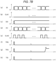
FIG. 7A is an operation timing chart of the semiconductor integrated circuit device 3 in normal operation. FIG. 7B is an operation timing chart of the semiconductor integrated circuit device 3 in a case where the first clock line to the DUT 8 and the result comparator 142 fails.
In FIGS. 7A and 7B, portion (a) indicates the input data DI, portion (b) indicates the first clock signal CLK1, portion (c) indicates the output data DO, portion (d) indicates the expected value data EV, portion (e) indicates the second clock signal CLK2, portion (f) indicates the test result signal TRS, portion (g) indicates the test end signal TES, and portion (h) indicates the additional circuit output signal TIS.
Example when the result comparator 142 operates normally and there is no problem in the DUT 8
(Operation Timing Chart: FIG. 7A)
In the result comparator 142, after the start of the test, the high level H (“1”), which is an inverted signal of the initial value “0” of the result holding circuit 26, is input to the additional circuit 30 as signal FV, and thereafter, the high level H value is continuously output as the additional circuit output signal TIS. When the output data DO of the DUT 8 and the expected value data EV match with each other, the result holding circuit 26 outputs the low level L as the test result signal TRS, and thereafter, the test result signal TRS continues to hold the low level L as shown by the solid line while the output data DO of the DUT 8 and the expected value data EV continue to match. The test end signal TES holds the low level L during the test, but it shifts from the low level L to the high level H when the test is completed. The control circuit 12 now determines whether the DUT 8 has a problem or the test has not been performed normally. Since the test result signal TRS is the low level L and the additional circuit output signal TIS is the high level H at the end of the test, it is determined that there is no problem in the DUT 8 and the test has been performed normally and that the DUT 8 has passed the test.
Example when the result comparator 142 operates normally and there is a problem in the DUT 8
(Operation Timing Chart: FIG. 7A)
In the result comparator 142, after the start of the test, the high level H (“1”), which is an inverted signal of the initial value “0” of the result holding circuit 26, is input to the additional circuit 30, and this value is continuously output as the additional circuit output signal TIS. While the output data DO of the DUT 8 and the expected value data EV match with each other, the test result signal TRS continues to hold the low level L. For example, it is the region shown by the broken line A in FIG. 7A. However, if the DUT 8 is defective and the output data DO of the DUT 8 and the expected value data EV do not match with each other, the test result signal TRS becomes the high level H as shown by the broken line and continues to hold this high level H. The test end signal TES holds the low level L during the test, but it shifts from the low level L to the high level H when the test is completed. The control circuit 12 now determines whether the DUT 8 has a problem or the test has not been performed normally. Since the test result signal TRS is the high level H and the additional circuit output signal TIS is the high level H at the end of the test, it is determined that there is a problem in the DUT 8 but the test has been performed normally and that the DUT 8 has failed the test.
Example when the result comparator 142 does not operate normally
(When the Clock Line Fails: FIG. 7B)
When the clock line to the DUT 8 fails, the first clock signal CLK1 to the DUT 8 is (or appears to be) always the low level L as shown in portion (b) of FIG. 7B. Similarly, the first clock signal CLK1 supplied to the result comparator 142 also becomes the low level L. Since the operation of both the DUT 8 and the result comparator 142 is stopped, the additional circuit output signal TIS from the result comparator 142 continues as the initial value 0 of the additional circuit 30 (rather than the signal FV from the result holding circuit 26), that is the low level L. The test result signal TRS also continues to output the initial value 0 of the result holding circuit 26, that is the low level L. The test end signal TES holds the low level L during the test, but it shifts from the low level L to the high level H when the test is completed. The control circuit 12 now determines whether the DUT 8 has a problem or the test has not been performed normally. Since the additional circuit output signal TIS is the low level L at the end of the test, it is determined that the test has not been performed normally regardless of the value of the test result signal TRS and that the DUT 8 test fails.
(Effect of Second Embodiment)
In the second embodiment, when it is determined that the test indicates a failure, it is possible to further distinguish between (i) there being a problem in the DUT 8 and (ii) the testing itself not being performed normally.
(Third Embodiment)
FIG. 8A shows a circuit block diagram of a semiconductor integrated circuit device 4 according to the third embodiment. FIG. 8B is a circuit block diagram of a result comparator 143 according to the third embodiment.
In the semiconductor integrated circuit device 4, the result comparator 143 is provided instead of the result comparator 141 of the first embodiment and the result comparator 142 of the second embodiment. The test result signal TRS and the additional circuit output signal TIS are output from the result comparator 143.
As shown in FIG. 8B, the result comparator 143 according to the third embodiment includes an expected value comparison circuit 22 that can be connected to the DUT 8, an additional circuit 32 that is connected to the expected value comparison circuit 22 and whose initial value is set to the high level H (“1”), another additional circuit 34 whose initial value is set to the low level L (“0”), an AND gate 36 that is connected to both the additional circuit 32 and the additional circuit 34, an OR gate 38 that is connected to the AND gate 36, and a result holding circuit 40 that is connected to the OR gate 38 and whose initial value is set to the low level L (“0”). The output of the result holding circuit 40 is further connected to the OR gate 38. When the test is started, the high level H (“1”) is input to the additional circuit 34. Each of the additional circuit 32, the additional circuit 34, and the result holding circuit 40 includes a flip-flop circuit configuration, such as a D-type flip-flop. The first clock signal CLK1 is input to the additional circuit 32, the additional circuit 34, and the result holding circuit 40.
The expected value comparison circuit 22 compares the output data DO of the DUT 8 with the expected value data EV and outputs the expected value comparison data EO. The expected value comparison data EO is input to the additional circuit 32.
The output of the additional circuit 32 is input to the AND gate 36. The output of the additional circuit 34 is also input to the AND gate 36. The AND gate 36 outputs the logical product of the expected value comparison data EO and the additional circuit 34. The additional circuit 34 also outputs an additional circuit output signal TIS. By observing the additional circuit output signal TIS, the operating state of the result comparator 143 can be determined. If the test is normally started, the additional circuit output signal TIS changes from the low level L (“0”) to the high level H (“1”).
The output of the additional circuit 34 is input to the AND gate 36. The output of the AND gate 36 is input to the OR gate 38. The output of the OR gate 38 is input to the result holding circuit 40. The result holding circuit 40 outputs the test result signal TRS in response to the input of the first clock signal CLK1. The test result signal TRS is also input to the OR gate 38. That is, the output of the OR gate 38 becomes the OR output of the output of the AND gate 36 and the test result signal TRS.
If the test result signal TRS is the low level L and the additional circuit output signal TIS is the high level H, the control circuit 12 determines that there is no problem in the DUT 8 and that the test has been performed normally. If the test result signal TRS is the high level H and the additional circuit output signal TIS is the high level H, the control circuit 12 determines that there is a problem in the DUT 8 but the test has been performed normally. If the additional circuit output signal TIS is the low level L, the control circuit 12 determines that the test has not been performed normally.
FIG. 9A is operation timing chart of the semiconductor integrated circuit 4 in normal operation. FIG. 9B is an operation timing chart of the semiconductor integrated circuit 4 in a case where the clock line to the DUT 8 fails.
In FIGS. 9A and 9B, portion (a) indicates the input data DI, portion (b) indicates the first clock signal CLK1, portion (c) indicates the output data DO, portion (d) indicates the expected value data EV, portion (e) indicates the second clock signal CLK2, portion (f) indicates the test result signal TRS, portion (g) indicates the test end signal TES, and portion (h) indicates the additional circuit output signal TIS.
Example when the result comparator 143 operates normally and there is no problem in the DUT 8
(Operation Timing Chart: FIG. 9A)
In the result comparator 143, after the start of the test, the high level H (“1”) is input to the additional circuit 34 in the period indicated by the broken line D, and thereafter, the value is continuously output as the additional circuit output signal TIS. When the output data DO of the DUT 8 and the expected value data EV match with each other, the expected value comparison circuit 22 outputs the low level L, and the additional circuit 32 output becomes the low level L. The high level H output from the additional circuit 34 and the low level L output from the additional circuit 32 are input to the AND circuit 36. The output of the AND circuit 36 becomes the low level L and is input to the OR circuit 38. The output from the result holding circuit 40 whose initial value is the low level L is input to the OR circuit 38, and as a result, the output of the OR circuit 38 becomes the low level L and is input to the result holding circuit 40. In this way, the test result signal TRS from the result holding circuit 40 continues to hold the low level L as shown by the solid line while the output data DO of the DUT 8 and the expected value data EV match. The test end signal TES holds the low level L during the test, but it shifts from the low level L to the high level H when the test is completed. The control circuit 12 determines whether the DUT 8 has a problem or the test has been performed normally. Since the test result signal TRS is the low level L and the additional circuit output signal TIS is the high level H at the end of the test, it is determined that there is no problem in the DUT 8 and the test has been performed normally and that the DUT 8 has passed the test.
Example when the result comparator operates 143 normally and there is a problem in the DUT 8
(Operation Timing Chart: FIG. 9A)
In the result comparator 143, after the start of the test, the high level H (“1”) is input to the additional circuit 34, and thereafter, the value is continuously output as the additional circuit output signal TIS. When the output data DO of the DUT 8 and the expected value data EV match with each other, the expected value comparison circuit 22 outputs the low level L, and the additional circuit 32 becomes the low level L. The high level H output from the additional circuit 34 and the low level L output from the additional circuit 32 are input to the AND circuit 36. The output of the AND circuit 36 becomes the low level L and is input to the OR circuit 38. The output from the result holding circuit 40 whose initial value is the low level L is input to the OR circuit 38, and as a result, the output of the OR circuit 38 becomes the low level L and is input to the result holding circuit 40. The test result signal TRS from the result holding circuit 40 continues to hold the low level L while the output data DO of the DUT 8 and the expected value data EV match. For example, it is the range shown by the broken line A in FIG. 9A. However, if there is a problem in the DUT 8 and the output data DO of the DUT 8 and the expected value data EV do not match, the output from the expected value comparison circuit 22 becomes the high level H. The value of the additional circuit 32 becomes the high level H. As a result, the output of the AND circuit 36 becomes the high level H and the output of the OR circuit 38 also becomes the high level H. The result holding circuit 40 also becomes the high level H, and thereafter, the test result signal TRS becomes the high level H as shown by the broken line and continues to hold this high level H. The test end signal TES holds the low level L during the test, but it shifts from the low level L to the high level H when the test is completed. The control circuit 12 then determines whether the DUT 8 has a problem or the test has not been performed normally. Since the test result signal TRS is the high level H and the additional circuit output signal TIS is the high level H at the end of the test, it is determined that there is a problem in the DUT 8 and the test has been performed normally.
Example when the result comparator 143 does not operate normally
(When the Clock Line Fails: FIG. 9B)
When the clock line to the DUT 8 fails, the first clock signal CLK1 to the DUT 8 becomes the low level L as shown in (b) of FIG. 9B. The additional circuit output signal TIS continues to output the low level L, which is the initial value of the additional circuit 34. The test result signal TRS continues to output the low level L, which is the initial value of the result holding circuit 40. The test end signal TES holds the low level L during the test, but it shifts from the low level L to the high level H when the test is completed. The control circuit 12 then determines whether the DUT 8 has a problem or the test has not been performed normally. Since the additional circuit output signal TIS is the low level L at the end of the test, it is determined that the test has not been performed normally regardless of the value of the test result signal TRS.
(Effect of Third Embodiment)
The same or substantially the same effect as that of the second embodiment can be obtained in the third embodiment.
While certain embodiments have been described, these embodiments have been presented by way of example only and are not intended to limit the scope of the disclosure. Indeed, the novel embodiments described herein may be embodied in a variety of other forms; furthermore, various omissions, substitutions and changes in the form of the embodiments described herein may be made without departing from the spirit of the disclosure. The accompanying claims and their equivalents are intended to cover such forms or modifications as would fall within the scope and spirit of the disclosure.

Claims (13)

What is claimed is:
1. A semiconductor integrated circuit device, comprising:
a pattern generator configured to supply input data to a device-under-test;
a result comparator configured to compare output data from the device-under-test with expected value data and output a test result signal;
a control circuit that controls the pattern generator and the result comparator, wherein
the device-under-test and the result comparator are connected to a first clock line, and
the pattern generator and the control circuit are connected to a second clock line different from the first clock line,
the result comparator comprises:
an expected value comparison circuit configured to compare the output data of the device-under-test with the expected value data and output expected value comparison data;
a result holding circuit configured to hold the expected value comparison data from the expected value comparison circuit and output the test result signal; and
a second additional circuit connected to the first clock line and configured to receive a first signal related to the result holding circuit and output an additional circuit output signal, an initial state of the second additional circuit being a state in which the additional circuit output signal is output at a first signal level, and
the control circuit is further configured to:
determine that the test has not been performed normally if the additional circuit output signal from the result comparator is the first signal level at the end of the test,
determine that the test has been performed normally and that the device-under-test has passed the test if the additional circuit output signal from the result comparator is a second signal level different from the first signal level at the end of the test and the test result signal from the result comparator is the first signal level, and
determine that the test has been performed normally and that the device-under-test has failed the test if the additional circuit output signal from the result comparator is the second signal level at the end of the test and the test result signal from the result comparator is the second signal level.
2. The semiconductor integrated circuit device according to claim 1, further comprising:
an OR circuit configured to receive the test result signal of the result holding circuit and the expected value comparison data of the expected value comparison circuit and supply an OR output to the result holding circuit.
3. The semiconductor integrated circuit device according to claim 1, wherein the result holding circuit has an initial state in which the first signal level is output from the result holding circuit.
4. The semiconductor integrated circuit device according to claim 1, wherein the control circuit includes a monitor terminal for observing the test result signal.
5. The semiconductor integrated circuit device according to claim 1, wherein the device-under-test is in the semiconductor integrated circuit device.
6. A semiconductor integrated circuit device, comprising:
a pattern generator configured to supply input data to a device-under-test;
a result comparator configured to compare output data from the device-under-test with expected value data and output a test result signal; and
a control circuit that controls the pattern generator and the result comparator, wherein
the device-under-test and the result comparator are connected to a first clock line,
the pattern generator and the control circuit are connected to a second clock line different from the first clock line,
the result comparator comprises:
an expected value comparison circuit configured to compare the output data of the device-under-test with the expected value data and output expected value comparison data;
a third additional circuit connected to an output of the expected value comparison circuit;
a fourth additional circuit configured to output an additional circuit output signal, the fourth additional circuit having an initial state in which the first signal level is output as the additional circuit output signal, and the additional circuit output signal transitioning to the second signal level after the start of the test; and
a result holding circuit connected to an output the third additional circuit and configured to output the test result signal, and
the control circuit is further configured to:
determine that the test has been performed normally and that the device-under-test has passed the test if the additional circuit output signal is the second signal level at the end of the test and the test result signal from the result comparator is the first signal level;
determine that the test has been performed normally and that the device-under-test has failed the test if the additional circuit output signal is the second signal level at the end of the test and the test result signal from the result comparator is the second signal level; and
determine that the test has not been performed normally if the additional circuit output signal is the first signal level at the end of the test.
7. The semiconductor integrated circuit device according to claim 6, further comprising:
an AND circuit configured to receive the output of the third additional circuit and the additional circuit output signal of the fourth additional circuit; and
an OR circuit configured to receive the test result signal of the result holding circuit and an output of the AND circuit and supply an OR output to the result holding circuit.
8. The semiconductor integrated circuit device according to claim 6, wherein the result holding circuit has an initial state in which the first signal level is output as the test result signal.
9. The semiconductor integrated circuit device according to claim 6, wherein the control circuit includes a monitor terminal for observing the test result signal.
10. The semiconductor integrated circuit device according to claim 6, wherein the device-under-test is in the semiconductor integrated circuit device.
11. An operating method for a semiconductor integrated circuit device, the method comprising:
comparing output data of a device-under-test and expected value data in an expected value comparison circuit;
holding a result of the comparing in a result holding circuit;
outputting a test result signal from the result holding circuit;
outputting an additional circuit output signal from an additional circuit, the additional circuit output signal being based on at least one of the test result signal and a first signal related to the result holding circuit;
determining that a test has not been performed normally if the additional circuit output signal is a first signal level at the end of the test;
determining that the test has been performed normally and that the device-under-test has passed the test if the additional circuit output signal is a second signal level, different from the first signal level, at the end of the test and the test result signal is the first signal level at the end of the test; and
determining that the test has been performed normally and that the device-under-test has failed the test if the additional circuit output signal is the second signal level at the end of the test and the test result signal is the second signal level at the end of the test.
12. The operating method according to claim 11, further comprising:
setting an initial state of the result holding circuit to a state in which the first signal level is generated.
13. The operating method according to claim 11, further comprising:
outputting the test result signal to a monitor terminal.
US17/410,744 2021-01-28 2021-08-24 Semiconductor integrated circuit device and operating method thereof Active 2041-10-22 US11740285B2 (en)

Applications Claiming Priority (2)

Application Number Priority Date Filing Date Title
JP2021011674A JP2022115179A (en) 2021-01-28 2021-01-28 Semiconductor integrated circuit device, and operation method of the same
JP2021-011674 2021-01-28

Publications (2)

Publication Number Publication Date
US20220236324A1 US20220236324A1 (en) 2022-07-28
US11740285B2 true US11740285B2 (en) 2023-08-29

Family

ID=82495620

Family Applications (1)

Application Number Title Priority Date Filing Date
US17/410,744 Active 2041-10-22 US11740285B2 (en) 2021-01-28 2021-08-24 Semiconductor integrated circuit device and operating method thereof

Country Status (4)

Country Link
US (1) US11740285B2 (en)
JP (1) JP2022115179A (en)
CN (1) CN114814519B (en)
TW (1) TWI790663B (en)

Families Citing this family (2)

* Cited by examiner, † Cited by third party
Publication number Priority date Publication date Assignee Title
JP2022115179A (en) * 2021-01-28 2022-08-09 キオクシア株式会社 Semiconductor integrated circuit device, and operation method of the same
US12231985B2 (en) * 2022-04-07 2025-02-18 Ecolink Intelligent Technology, Inc. Method and apparatus for location-based, automated control of electronic devices

Citations (30)

* Cited by examiner, † Cited by third party
Publication number Priority date Publication date Assignee Title
JPH09127206A (en) 1995-09-18 1997-05-16 Internatl Business Mach Corp <Ibm> Method and integrated self-test device for integrated circuit testing to capture fault information about selected faults
US5640509A (en) 1995-10-03 1997-06-17 Intel Corporation Programmable built-in self-test function for an integrated circuit
US5642317A (en) * 1995-05-16 1997-06-24 Mitsubishi Denki Kabushiki Kaisha Semiconductor memory device incorporating a test mechanism
JPH11344535A (en) 1998-06-02 1999-12-14 Toshiba Corp Semiconductor integrated circuit device
US6631486B1 (en) * 1998-09-29 2003-10-07 Matsushita Electric Industrial Co., Ltd. Semiconductor integrated circuit and method for testing the same
US20030191998A1 (en) * 2002-04-03 2003-10-09 Yoshiyuki Nakamura Built-in self test circuit
JP2004061114A (en) 2002-07-24 2004-02-26 Matsushita Electric Ind Co Ltd Self-diagnosis test circuit and method
US20040193991A1 (en) * 2003-01-08 2004-09-30 Kabushiki Kaisha Toshiba Semiconductor integrated circuit including operation test circuit and operation test method thereof
US20060282731A1 (en) * 2005-05-26 2006-12-14 Nec Electronics Corporation Semiconductor integrated circuit and method of testing same
US20070022346A1 (en) * 2004-01-29 2007-01-25 Advantest Corporation Test apparatus and test method
US20070091497A1 (en) * 2005-10-25 2007-04-26 Makio Mizuno Control of storage system using disk drive device having self-check function
US20080022176A1 (en) * 2006-07-07 2008-01-24 Kabushiki Kaisha Toshiba Semiconductor integrated circuit
US20080077831A1 (en) * 2006-09-27 2008-03-27 Nec Electronics Corporation Semiconductor integrated circuit, BIST circuit, design program of BIST circuit, design device of BIST circuit and test method of memory
US20080141089A1 (en) * 2005-01-27 2008-06-12 Yasuteru Maeda Semiconductor Integrated Circuit and System Lsi
US20090115443A1 (en) 2007-11-01 2009-05-07 Kingtiger Technology (Canada) Inc. System and method for testing integrated circuit modules comprising a plurality of integrated circuit devices
US20100107026A1 (en) * 2008-10-24 2010-04-29 Nec Electronics Corporation Semiconductor device having built-in self-test circuit and method of testing the same
US20100148815A1 (en) * 2007-05-14 2010-06-17 Advantest Corporation Test apparatus
US20100182857A1 (en) * 2009-01-21 2010-07-22 Elpida Memory, Inc. Tester for semiconductor device and semiconductor device
US7765449B2 (en) * 2004-08-20 2010-07-27 Advantest Corporation Test apparatus that tests a plurality of devices under test having plural memory cells and test method therefor
US20100207640A1 (en) * 2007-08-20 2010-08-19 Advantest Corporation Test apparatus, test method and manufacturing method
US7805641B2 (en) * 2005-12-28 2010-09-28 Advantest Corporation Test apparatus for regulating a test signal supplied to a device under test and method thereof
US8111082B2 (en) * 2008-06-09 2012-02-07 Advantest Corporation Test apparatus
US8502523B2 (en) * 2008-09-05 2013-08-06 Advantest Corporation Test apparatus and test method
US20130200931A1 (en) * 2010-09-17 2013-08-08 Fujitsu Limited Circuit device, frequency changing circuit, method of testing circuit device, and method of controlling frequency changing circuit
US8719650B2 (en) 2010-04-23 2014-05-06 Renesas Electronics Corporation Self-diagnosis system and test circuit determination method
US20140289576A1 (en) 2013-03-25 2014-09-25 Kabushiki Kaisha Toshiba Semiconductor integrated circuit and method for self test of semiconductor integrated circuit
JP5727358B2 (en) 2011-12-22 2015-06-03 ルネサスエレクトロニクス株式会社 Semiconductor device
US20170192057A1 (en) 2016-01-05 2017-07-06 International Business Machines Corporation Logic built in self test circuitry for use in an integrated circuit with scan chains
US20180277237A1 (en) * 2017-03-21 2018-09-27 Renesas Electronics Corporation Semiconductor device and diagnostic method therefor
US20220236324A1 (en) * 2021-01-28 2022-07-28 Kioxia Corporation Semiconductor integrated circuit device and operating method thereof

Family Cites Families (5)

* Cited by examiner, † Cited by third party
Publication number Priority date Publication date Assignee Title
JP3558228B2 (en) * 1994-05-31 2004-08-25 株式会社アドバンテスト Semiconductor test method and apparatus for performing the same
CN1223443A (en) * 1998-01-16 1999-07-21 三菱电机株式会社 semiconductor integrated circuit device
JP2007322141A (en) * 2006-05-30 2007-12-13 Yokogawa Electric Corp Semiconductor integrated circuit test apparatus and method
JP2008118297A (en) * 2006-11-01 2008-05-22 Matsushita Electric Ind Co Ltd Digital video data inspection system and semiconductor device
JP5863160B2 (en) * 2010-12-21 2016-02-16 ローム株式会社 Control circuit and data holding device using the same

Patent Citations (34)

* Cited by examiner, † Cited by third party
Publication number Priority date Publication date Assignee Title
US5642317A (en) * 1995-05-16 1997-06-24 Mitsubishi Denki Kabushiki Kaisha Semiconductor memory device incorporating a test mechanism
JPH09127206A (en) 1995-09-18 1997-05-16 Internatl Business Mach Corp <Ibm> Method and integrated self-test device for integrated circuit testing to capture fault information about selected faults
US5912901A (en) 1995-09-18 1999-06-15 International Business Machines Corporation Method and built-in self-test apparatus for testing an integrated circuit which capture failure information for a selected failure
US5640509A (en) 1995-10-03 1997-06-17 Intel Corporation Programmable built-in self-test function for an integrated circuit
JPH11344535A (en) 1998-06-02 1999-12-14 Toshiba Corp Semiconductor integrated circuit device
US6631486B1 (en) * 1998-09-29 2003-10-07 Matsushita Electric Industrial Co., Ltd. Semiconductor integrated circuit and method for testing the same
US20030191998A1 (en) * 2002-04-03 2003-10-09 Yoshiyuki Nakamura Built-in self test circuit
JP2004061114A (en) 2002-07-24 2004-02-26 Matsushita Electric Ind Co Ltd Self-diagnosis test circuit and method
US20040193991A1 (en) * 2003-01-08 2004-09-30 Kabushiki Kaisha Toshiba Semiconductor integrated circuit including operation test circuit and operation test method thereof
US20070022346A1 (en) * 2004-01-29 2007-01-25 Advantest Corporation Test apparatus and test method
US7765449B2 (en) * 2004-08-20 2010-07-27 Advantest Corporation Test apparatus that tests a plurality of devices under test having plural memory cells and test method therefor
US20080141089A1 (en) * 2005-01-27 2008-06-12 Yasuteru Maeda Semiconductor Integrated Circuit and System Lsi
US20060282731A1 (en) * 2005-05-26 2006-12-14 Nec Electronics Corporation Semiconductor integrated circuit and method of testing same
US20070091497A1 (en) * 2005-10-25 2007-04-26 Makio Mizuno Control of storage system using disk drive device having self-check function
US7805641B2 (en) * 2005-12-28 2010-09-28 Advantest Corporation Test apparatus for regulating a test signal supplied to a device under test and method thereof
US20080022176A1 (en) * 2006-07-07 2008-01-24 Kabushiki Kaisha Toshiba Semiconductor integrated circuit
US20080077831A1 (en) * 2006-09-27 2008-03-27 Nec Electronics Corporation Semiconductor integrated circuit, BIST circuit, design program of BIST circuit, design device of BIST circuit and test method of memory
US20100148815A1 (en) * 2007-05-14 2010-06-17 Advantest Corporation Test apparatus
US20100207640A1 (en) * 2007-08-20 2010-08-19 Advantest Corporation Test apparatus, test method and manufacturing method
US8373433B2 (en) * 2007-08-20 2013-02-12 Advantest Corporation Test apparatus, test method and manufacturing method
TWI435096B (en) 2007-11-01 2014-04-21 皇虎科技(加拿大)有限公司 System and method for testing an integrated circuit module including a plurality of integrated circuit devices
US20090115443A1 (en) 2007-11-01 2009-05-07 Kingtiger Technology (Canada) Inc. System and method for testing integrated circuit modules comprising a plurality of integrated circuit devices
US8111082B2 (en) * 2008-06-09 2012-02-07 Advantest Corporation Test apparatus
US8502523B2 (en) * 2008-09-05 2013-08-06 Advantest Corporation Test apparatus and test method
US20100107026A1 (en) * 2008-10-24 2010-04-29 Nec Electronics Corporation Semiconductor device having built-in self-test circuit and method of testing the same
US20100182857A1 (en) * 2009-01-21 2010-07-22 Elpida Memory, Inc. Tester for semiconductor device and semiconductor device
US8719650B2 (en) 2010-04-23 2014-05-06 Renesas Electronics Corporation Self-diagnosis system and test circuit determination method
JP5608409B2 (en) 2010-04-23 2014-10-15 ルネサスエレクトロニクス株式会社 Self-diagnosis system and test circuit determination method
US20130200931A1 (en) * 2010-09-17 2013-08-08 Fujitsu Limited Circuit device, frequency changing circuit, method of testing circuit device, and method of controlling frequency changing circuit
JP5727358B2 (en) 2011-12-22 2015-06-03 ルネサスエレクトロニクス株式会社 Semiconductor device
US20140289576A1 (en) 2013-03-25 2014-09-25 Kabushiki Kaisha Toshiba Semiconductor integrated circuit and method for self test of semiconductor integrated circuit
US20170192057A1 (en) 2016-01-05 2017-07-06 International Business Machines Corporation Logic built in self test circuitry for use in an integrated circuit with scan chains
US20180277237A1 (en) * 2017-03-21 2018-09-27 Renesas Electronics Corporation Semiconductor device and diagnostic method therefor
US20220236324A1 (en) * 2021-01-28 2022-07-28 Kioxia Corporation Semiconductor integrated circuit device and operating method thereof

Also Published As

Publication number Publication date
JP2022115179A (en) 2022-08-09
TW202230385A (en) 2022-08-01
CN114814519B (en) 2025-07-04
US20220236324A1 (en) 2022-07-28
TWI790663B (en) 2023-01-21
CN114814519A (en) 2022-07-29

Similar Documents

Publication Publication Date Title
US6343366B1 (en) BIST circuit for LSI memory
KR100234504B1 (en) Integrated test method and integrated magnetic test device for capturing fault information on selected faults
US6928593B1 (en) Memory module and memory component built-in self test
US11740285B2 (en) Semiconductor integrated circuit device and operating method thereof
JP2002267721A (en) Test apparatus and method for CPU embedded RAM embedded LSI
CN114360622B (en) Reset circuit testing system and method for logic built-in self-test
US20100275076A1 (en) Semiconductor integrated circuit and testing method for the same
US7096386B2 (en) Semiconductor integrated circuit having functional modules each including a built-in self testing circuit
US6226764B1 (en) Integrated circuit memory devices including internal stress voltage generating circuits and methods for built-in self test (BIST)
US10191110B2 (en) Apparatus and method for self-testing an integrated circuit
US9805826B2 (en) Method and apparatus for testing integrated circuit
JP2000030495A (en) Fully on-chip wafer level burn-in test circuit and method thereof
US11579191B2 (en) Method and system for testing an integrated circuit
US10747282B2 (en) Test circuit for electronic device permitting interface control between two supply stacks in a production test of the electronic device
EP4575531A1 (en) System and method for validating critical paths of integrated circuits
KR100896763B1 (en) Semiconductor device test device
US7511509B2 (en) Semiconductor device and test system which output fuse cut information sequentially
US20180259578A1 (en) Method and apparatus for dynamic controller bist
US20080077827A1 (en) Test method for semiconductor device
KR20020068768A (en) Semiconductor device having built-in self repair circuit for embedded memory
US6976198B1 (en) Self-repairing integrated circuit and method of operating the same
US20140281764A1 (en) Data path memory test
US8531200B2 (en) Semiconductor device for performing test operation and method thereof
US7930602B2 (en) Method and system for performing a double pass NTH fail bitmap of a device memory
JPH11174125A (en) Semiconductor test circuit

Legal Events

Date Code Title Description
FEPP Fee payment procedure

Free format text: ENTITY STATUS SET TO UNDISCOUNTED (ORIGINAL EVENT CODE: BIG.); ENTITY STATUS OF PATENT OWNER: LARGE ENTITY

STPP Information on status: patent application and granting procedure in general

Free format text: DOCKETED NEW CASE - READY FOR EXAMINATION

AS Assignment

Owner name: KIOXIA CORPORATION, JAPAN

Free format text: ASSIGNMENT OF ASSIGNORS INTEREST;ASSIGNOR:TAKAHASHI, YUUSUKE;REEL/FRAME:058339/0565

Effective date: 20211125

STPP Information on status: patent application and granting procedure in general

Free format text: NON FINAL ACTION MAILED

STPP Information on status: patent application and granting procedure in general

Free format text: NOTICE OF ALLOWANCE MAILED -- APPLICATION RECEIVED IN OFFICE OF PUBLICATIONS

STCF Information on status: patent grant

Free format text: PATENTED CASE