US11727253B2 - Neural network system including gate circuit for controlling memristor array circuit - Google Patents
Neural network system including gate circuit for controlling memristor array circuit Download PDFInfo
- Publication number
- US11727253B2 US11727253B2 US16/682,420 US201916682420A US11727253B2 US 11727253 B2 US11727253 B2 US 11727253B2 US 201916682420 A US201916682420 A US 201916682420A US 11727253 B2 US11727253 B2 US 11727253B2
- Authority
- US
- United States
- Prior art keywords
- output
- neural network
- network system
- circuit
- data
- Prior art date
- Legal status (The legal status is an assumption and is not a legal conclusion. Google has not performed a legal analysis and makes no representation as to the accuracy of the status listed.)
- Active, expires
Links
Images


Classifications
-
- G—PHYSICS
- G06—COMPUTING; CALCULATING OR COUNTING
- G06N—COMPUTING ARRANGEMENTS BASED ON SPECIFIC COMPUTATIONAL MODELS
- G06N3/00—Computing arrangements based on biological models
- G06N3/02—Neural networks
- G06N3/06—Physical realisation, i.e. hardware implementation of neural networks, neurons or parts of neurons
- G06N3/063—Physical realisation, i.e. hardware implementation of neural networks, neurons or parts of neurons using electronic means
-
- G—PHYSICS
- G06—COMPUTING; CALCULATING OR COUNTING
- G06N—COMPUTING ARRANGEMENTS BASED ON SPECIFIC COMPUTATIONAL MODELS
- G06N3/00—Computing arrangements based on biological models
- G06N3/02—Neural networks
- G06N3/04—Architecture, e.g. interconnection topology
-
- G—PHYSICS
- G06—COMPUTING; CALCULATING OR COUNTING
- G06N—COMPUTING ARRANGEMENTS BASED ON SPECIFIC COMPUTATIONAL MODELS
- G06N3/00—Computing arrangements based on biological models
- G06N3/02—Neural networks
- G06N3/04—Architecture, e.g. interconnection topology
- G06N3/048—Activation functions
-
- G—PHYSICS
- G06—COMPUTING; CALCULATING OR COUNTING
- G06N—COMPUTING ARRANGEMENTS BASED ON SPECIFIC COMPUTATIONAL MODELS
- G06N3/00—Computing arrangements based on biological models
- G06N3/02—Neural networks
- G06N3/06—Physical realisation, i.e. hardware implementation of neural networks, neurons or parts of neurons
- G06N3/063—Physical realisation, i.e. hardware implementation of neural networks, neurons or parts of neurons using electronic means
- G06N3/065—Analogue means
-
- G—PHYSICS
- G11—INFORMATION STORAGE
- G11C—STATIC STORES
- G11C11/00—Digital stores characterised by the use of particular electric or magnetic storage elements; Storage elements therefor
- G11C11/54—Digital stores characterised by the use of particular electric or magnetic storage elements; Storage elements therefor using elements simulating biological cells, e.g. neuron
-
- G—PHYSICS
- G11—INFORMATION STORAGE
- G11C—STATIC STORES
- G11C13/00—Digital stores characterised by the use of storage elements not covered by groups G11C11/00, G11C23/00, or G11C25/00
- G11C13/0002—Digital stores characterised by the use of storage elements not covered by groups G11C11/00, G11C23/00, or G11C25/00 using resistive RAM [RRAM] elements
- G11C13/0021—Auxiliary circuits
- G11C13/003—Cell access
-
- G—PHYSICS
- G11—INFORMATION STORAGE
- G11C—STATIC STORES
- G11C13/00—Digital stores characterised by the use of storage elements not covered by groups G11C11/00, G11C23/00, or G11C25/00
- G11C13/0002—Digital stores characterised by the use of storage elements not covered by groups G11C11/00, G11C23/00, or G11C25/00 using resistive RAM [RRAM] elements
- G11C13/0021—Auxiliary circuits
- G11C13/0069—Writing or programming circuits or methods
-
- G—PHYSICS
- G06—COMPUTING; CALCULATING OR COUNTING
- G06N—COMPUTING ARRANGEMENTS BASED ON SPECIFIC COMPUTATIONAL MODELS
- G06N3/00—Computing arrangements based on biological models
- G06N3/02—Neural networks
- G06N3/08—Learning methods
-
- G—PHYSICS
- G11—INFORMATION STORAGE
- G11C—STATIC STORES
- G11C2213/00—Indexing scheme relating to G11C13/00 for features not covered by this group
- G11C2213/70—Resistive array aspects
- G11C2213/79—Array wherein the access device being a transistor
Definitions
- Embodiments of the inventive concept disclosed herein relate to a neural network system, and more particularly, relate to a neural network system including a memristor array circuit.
- a neural network refers to an algorithm for modeling the human brain and an electronic circuit/device/system for implementing the algorithm.
- the neural network includes a large number of neurons as a basic unit, and the neurons transfer signals to other neurons through synapses.
- the neural network is used to perform machine learning.
- the neural network may perform learning based on input training data. For example, the neural network may learn a feature and a pattern of the input training data.
- the neural network may generate an answer to a newly input question based on the learning.
- the training of the neural network may be classified into pre-training and re-training.
- the pre-training is performed on all the neurons of the neural network under the same conditions, but the re-training is individually performed on neurons based on features of the respective neurons. Accordingly, costs necessary to perform the re-training increase. For this reason, there is required a technology for reducing costs of the re-training.
- Embodiments of the inventive concept provide a neural network system including a gate circuit for selectively activating memory cells included in a memristor array circuit.
- a neural network system may include an array circuit.
- the array circuit may generate output data based on first input data, by a plurality of memory cells.
- the gate circuit may output a select signal, based on defect information which is obtained based on the output data.
- a target memory cell, which is activated in response to the select signal, from among the plurality of memory cells may be trained based on second input data, and the defect information may be associated with a defect included in the plurality of memory cells.
- a neural network system may include a gate circuit and an array circuit. Based on defect information, the gate circuit may output a select signal of a first logical value for activating a target column or may output the select signal of a second logical value for deactivating the target column.
- the array circuit may generate output data corresponding to input data, by the target column which is programmed by the input data in response to the select signal of the first logical value.
- the defect information may be associated with an error included in the output data.
- a neural network system may include a gate circuit and an array circuit. Based on defect information, the gate circuit may output a select signal to a first column during a first time period and may output the select signal to a second column during a second time period after the first time period.
- the array circuit may include the first column and the second column, each of which generates an output voltage in response to the select signal of the first logical value and is deactivated in response to the select signal of the second logical value.
- the defect information may be associated with the output data.
- FIG. 1 is a block diagram illustrating a neural network system according to an embodiment of the inventive concept.
- FIG. 2 is a flowchart illustrating example operations of a processor and a neural network system of FIG. 1 .
- FIG. 3 is a block diagram illustrating an example configuration of a pulse generating circuit of FIG. 1 .
- FIG. 4 is a block diagram illustrating an example configuration of a gate circuit of FIG. 1 .
- FIG. 5 is a circuit diagram illustrating an example configuration of a dendritic gate of FIG. 4 .
- FIGS. 6 to 9 are circuit diagrams illustrating example operations of a dendritic gate of FIG. 4 .
- FIG. 10 is a circuit diagram illustrating an example configuration of a memristor array circuit of FIG. 1 .
- FIGS. 11 and 12 are circuit diagrams illustrating example operations of a memristor array circuit of FIG. 10 .
- FIG. 13 is a circuit diagram illustrating an example configuration of a calculating circuit of FIG. 1 .
- FIG. 14 is a block diagram illustrating an example electronic device according to an embodiment of the inventive concept.
- circuits may be connected with any other components in addition to components illustrated in drawings or disclosed in the detailed description. Connections between circuits or components may be direct or indirect. Circuits or components may be connected through respective communication or may be physically connected.
- FIG. 1 is a block diagram illustrating a neural network system according to an embodiment of the inventive concept.
- a neural network system 1000 may include an input circuit 1100 , a memristor array circuit 1200 , a calculating circuit 1300 , a pulse generating circuit 1400 , a gate controlling circuit 1500 , and a gate circuit 1600 .
- the neural network system 1000 may be a component of an electronic device (refer to FIG. 14 ).
- the electronic device including the neural network system 1000 may be one of a personal computer (PC), a workstation, a notebook computer, a mobile device, etc.
- the input circuit 1100 may generate a voltage VIN.
- An example is illustrated in FIG. 1 as the voltage VIN is a single voltage.
- the input circuit 1100 may generate one or more voltages, and the voltage VIN may include the one or more voltages generated by the input circuit 1100 .
- the one or more voltages may be respectively output to rows including memory cells of the memristor array circuit 1200 .
- the electronic device including the neural network system 1000 may include a processor 10 .
- the processor 10 may generate data for learning and training of the neural network system 1000 based on various logic circuits.
- the processor 10 may generate data for pre-training of the neural network system 1000 .
- the processor 10 may generate data for re-training of the neural network system 1000 .
- training means programming a weight in the memristor array circuit 1200 .
- the training of the memristor array circuit 1200 may include the pre-training and the re-training.
- the pre-training means programming a weight in the memristor array circuit 1200 for the first time.
- the processor 10 may generate data for the purpose of the pre-training for an ideal state (i.e., a state where memory cells do not include a defect) of the memory cells constituting the memristor array circuit 1200 .
- the re-training means reprogramming the memristor array circuit 1200 for the purpose of decreasing an error of data output from the memristor array circuit 1200 .
- the processor 10 may obtain information about defects included in the memory cells of the memristor array circuit 1200 (e.g., mapping information about defects of the memory cells) and may generate data for the purpose of performing the re-training on memory cells that are determined as including a defect. By performing the re-training in which defects of memory cells are considered, data that the memristor array circuit 1200 will output may include an error of a smaller magnitude.
- the processor 10 may output a signal IDAT indicating data generated for the pre-training and/or the re-training, to the input circuit 1100 .
- the input circuit 1100 may generate the voltage VIN indicating data for the pre-training and/or the re-training in response to the signal IDAT.
- the input circuit 1100 may output the voltage VIN to the memristor array circuit 1200 in the unit of row.
- the processor 10 may output the signal IDAT indicating input data to the input circuit 1100 for the purpose of obtaining result data from the learned and trained memristor array circuit 1200 .
- the input data may refer to data that are input by a user for the purpose of solving a particular question or the like.
- the result data may refer to data that are output by the neural network system 1000 in response to the input data.
- the input circuit 1100 may generate the voltage VIN indicating the input data based on the signal IDAT output from the processor 10 .
- the input circuit 1100 may output the voltage VIN indicating the input data to the memristor array circuit 1200 in the unit of row.
- the memristor array circuit 1200 may include a plurality of memory cells.
- each of the plurality of memory cells may be implemented with a memristor component.
- the memristor array circuit 1200 may include a memory cell array formed with a memristor crossbar structure.
- the memristor array circuit 1200 may receive the voltage VIN from the input circuit 1100 .
- the memory cells of the memristor array circuit 1200 may have characteristic values that vary with the voltage VIN.
- each of the memory cells may include a memristor component, and device values of the memristor components may vary with the voltage VIN that is supplied in the unit of row.
- Each memory cell may store data based on a varying characteristic value.
- a memristor resistance having a resistance value as a characteristic value will be described as an embodiment of the memristor component, but the inventive concept is not limited thereto.
- the memristor component of the inventive concept may be implemented with various kinds of memory devices having a characteristic value that varies with supplied voltage and current.
- the memristor array circuit 1200 may receive a signal SEL from the gate circuit 1600 .
- the signal SEL may include one or more signals.
- the signal SEL may include signals respectively corresponding to columns of the memristor array circuit 1200 .
- the memristor array circuit 1200 may operate in the unit of column based on the signal SEL.
- the memristor array circuit 1200 may output a voltage VOUT based on the voltage VIN.
- the voltage VIN may indicate the input data generated by the processor 10 .
- Learned and trained memory cells of the memristor array circuit 1200 may generate the voltage VOUT indicating output data, based on the voltage VIN.
- the memristor array circuit 1200 may output the voltage VOUT to the calculating circuit 1300 .
- the voltage VOUT is one voltage, but the voltage VOUT may include one or more voltages indicating the output data.
- the memristor array circuit 1200 may output voltages, which are generated by columns selected by the signal SEL, as the voltage VOUT. That is, one or more voltages indicated as the voltage VOUT in FIG. 1 may respectively correspond to one or more columns including the memory cells of the memristor array circuit 1200 .
- the memory cells of the memristor array circuit 1200 may have defects coming from various causes. For example, the memory cells may have a defects coming from a process error. Due to memory cells having defects, the memristor array circuit 1200 may generate the output data including an error based on the voltage VIN. Accordingly, it is necessary to perform the re-training on memory cells having defects.
- the calculating circuit 1300 may receive the voltage VOUT indicating the output data from the memristor array circuit 1200 .
- the calculating circuit 1300 may obtain result data by calculating the output data based on an activation function.
- the calculating circuit 1300 may generate a signal ODAT for transferring the result data.
- the calculating circuit 1300 may include electronic circuits configured to perform a calculation on the output data based on the activation function.
- the calculating circuit 1300 may include electronic circuits configured to implement calculations of various types of activation functions such as a sigmoid function and a rectified linear unit (ReLU) function, but embodiments of the inventive concept are not limited thereto.
- An example configuration and example operations of the calculating circuit 1300 will be more fully described with reference to FIG. 13 .
- the pulse generating circuit 1400 may receive a signal PSI including a pulse from the outside of the neural network system 1000 .
- the pulse generating circuit 1400 may receive the signal PSI from a function generator provided outside the neural network system 1000 .
- the pulse generating circuit 1400 may generate a signal PS including at least one pulse based on the signal PSI.
- the pulse generating circuit 1400 may generate the signal PS including signals respectively corresponding to the columns of the memristor array circuit 1200 .
- the pulse generating circuit 1400 may output the signal PS to the gate circuit 1600 .
- An example configuration and example operations of the pulse generating circuit 1400 will be more fully described with reference to FIG. 3 .
- the gate controlling circuit 1500 may receive a signal CS from the processor 10 .
- the gate controlling circuit 1500 may generate signals ST, STB, and EXE for controlling the gate circuit 1600 based on the signal CS.
- the gate controlling circuit 1500 may output the signals ST, STB, and EXE to the gate circuit 1600 .
- the signals ST and STB may have complementary logical values.
- the gate controlling circuit 1500 may adjust a level of an operation voltage that is supplied to the gate circuit 1600 .
- the processor 10 may select columns targeted for the re-training from among the columns included in the memristor array circuit 1200 , based on the signal ODAT received from the calculating circuit 1300 . For example, the processor 10 may obtain result data based on the signal ODAT. The processor 10 may obtain defect information about respective memory cells of the memristor array circuit 1200 , based on the obtained result data. The processor 10 may perform various logic-based calculations for the purpose of obtaining the defect information based on the result data.
- the defect information refers to information indicating whether any memory cells of the memory cells included in the memristor array circuit 1200 include defects.
- the defect information may include information indicating memory cells, in which the degree of contribution to an error of the result data is a reference value or greater, from among the memory cells of the memristor array circuit 1200 .
- the processor 10 may select columns targeted for the re-training from among the columns of the memristor array circuit 1200 , based on the obtained defect information.
- the processor 10 may output the signal CS for the purpose of controlling the memristor array circuit 1200 such that the re-training is performed only on the selected columns and may adjust a level of the operation voltage provided to the gate circuit 1600 .
- the processor 10 may output the signal CS including the defect information to the gate controlling circuit 1500 .
- the gate controlling circuit 1500 may adjust a level of the operation voltage to be supplied to the gate circuit 1600 for the purpose of programming the gate circuit 1600 based on the obtained defect information.
- Example operations of the gate controlling circuit 1500 for controlling the gate circuit 1600 based on the signals ST, STB, and EXE will be more fully described with reference to FIGS. 4 to 9 .
- the gate circuit 1600 may receive the signals ST, STB, and EXE from the gate controlling circuit 1500 .
- the gate circuit 1600 may output the signal SEL having a particular logical value to the memristor array circuit 1200 based on the signals ST, STB, and EXE.
- the signals ST and STB may be associated with whether a particular column of the memristor array circuit 1200 is targeted for the re-training.
- the signal EXE may be associated with whether to activate all the columns of the memristor array circuit 1200 .
- the gate circuit 1600 may output the signal SEL having a logical value of “1” to columns of the memristor array circuit 1200 targeted for the re-training and may output the signal SEL having a logical value of “0” to columns of the memristor array circuit 1200 not targeted for the re-training.
- the gate circuit 1600 may output the signal SEL having a logical value of “1” for the purpose of performing the pre-training or for the purpose of performing an inference operation on any input data input by the user.
- FIG. 2 is a flowchart illustrating example operations of a processor and a neural network system of FIG. 1 .
- the pre-training may be performed on the memristor array circuit 1200 .
- the processor 10 may generate input data for the pre-training of the memristor array circuit 1200 .
- the input data for the pre-training may be generated without consideration of defects included in memory cells of the memristor array circuit 1200 .
- the processor 10 may output the signal IDAT indicating the input data for the pre-training.
- the input circuit 1100 may output the voltage VIN based on the signal IDAT.
- the processor 10 may output the signal CS to control the gate controlling circuit 1500 , such that the pre-training is performed on all the columns of the memristor array circuit 1200 .
- the gate controlling circuit 1500 may output the signal EXE based on the signal CS.
- the gate circuit 1600 may output the signal SEL having a logical value that is determined based on the signal EXE.
- the processor 10 may output the signal IDAT indicating the input data for the pre-training to the input circuit 1100 .
- the input circuit 1100 may output the voltage VIN based on the signal IDAT.
- the pre-training may be performed such that characteristic values of the memory cells included in the memristor array circuit 1200 are changed based on the voltage VIN.
- defect information about the memory cells of the memristor array circuit 1200 may be obtained.
- the calculating circuit 1300 may generate the signal ODAT based on the voltage VOUT output from the memristor array circuit 1200 having the characteristic values changed by the pre-training.
- the processor 10 may calculate an error included in output data of the voltage VOUT based on result data of the signal ODAT.
- the processor 10 may calculate the degree of contribution to the error included in the output data in the unit of memory cells and/or in the unit of column.
- the error may be associated with a difference between result data intended by the user and result data actually obtained based on the signal ODAT.
- the expression “difference” means a conceptual difference rather than an arithmetic difference.
- the user may input an answer (i.e., the result data intended by the user) to a predefined question (i.e., input data) to the processor 10 .
- the processor 10 may compare the output data intended by the user and the result data received from the calculating circuit 1300 to calculate an error.
- the processor 10 may calculate an error through logic circuits implementing various types of error functions.
- the processor 10 may obtain the result data in the unit of column of the memristor array circuit 1200 .
- the processor 10 may calculate errors respectively corresponding to the columns.
- the processor 10 may calculate the degrees of contribution of result data, which correspond to each column of the memristor array circuit 1200 , to an error based on various algorithms.
- the processor 10 may obtain defect information indicating columns (hereinafter referred to as “target columns”), each of which generates output data corresponding to result data in which the degree of contribution to an error is a reference value or greater.
- the re-training may be performed on the memristor array circuit 1200 .
- the processor 10 may output the signal IDAT indicating input data for the re-training.
- the input circuit 1100 may output the voltage VIN based on the signal IDAT.
- the processor 10 may output the signal CS to control the gate controlling circuit 1500 , such that the re-training is performed only on target columns based on the defect information obtained in operation S 120 .
- the gate controlling circuit 1500 may output the signals ST and STB based on the signal CS.
- the gate circuit 1600 may output the signal SEL having a logical value that is determined based on the signals ST and STB.
- An example configuration of the gate circuit 1600 will be more fully described with reference to FIG. 5 .
- Example operations of the gate controlling circuit 1500 and the gate circuit 1600 will be more fully described with reference to FIGS. 7 to 9 .
- the columns of the memristor array circuit 1200 may be selectively activated in response to the signal SEL.
- Target columns of the columns of the memristor array circuit 1200 may be activated in response to the signal SEL.
- the activated target columns may be re-trained based on the voltage VIN.
- An example is illustrated in FIG. 2 as operation S 130 is performed once, but it may be well understood that operation S 130 is repeatedly performed. For example, operation S 130 may be repeatedly performed until an error included in result data decreases to a threshold value or less.
- the neural network system 1000 may be used to obtain output data associated with any input data.
- the user may input, to the processor 10 , input data corresponding to a particular question for the purpose of obtaining an answer to the particular question.
- the processor 10 may output the signal IDAT indicating the input data.
- the processor 10 may output the signal CS and may control the gate controlling circuit 1500 such that all the columns of the memristor array circuit 1200 are activated.
- the gate controlling circuit 1500 may output the signal EXE based on the signal CS.
- the gate circuit 1600 may output the signal SEL having a logical value that is determined based on the signal EXE. All the columns of the memristor array circuit 1200 may be activated in response to the signal SEL.
- the memristor array circuit 1200 may output the voltage VOUT indicating the output data corresponding to the input data.
- the calculating circuit 1300 may provide the result data to the processor 10 based on the output data.
- the processor 10 may provide the user with a variety of information about an answer to a particular question, based on the result data.
- FIG. 3 is a block diagram illustrating an example configuration of a pulse generating circuit of FIG. 1 .
- the pulse generating circuit 1400 may include flip-flops 1410 to 1430 .
- the pulse generating circuit 1400 may receive the signal PSI including a pulse from a signal generator provided outside the neural network system 1000 .
- the pulse generating circuit 1400 may receive a clock CLK from an electronic device such as a clock generator provided outside the neural network system 1000 .
- the flip-flops 1410 to 1430 may output signals PS 1 to PSn (n being a natural number) to the memristor array circuit 1200 based on the clock CLK and the signal PSI.
- the flip-flops 1410 to 1430 may output the signals PS 1 to PSn to the columns of the memristor array circuit 1200 , respectively.
- the pulse generating circuit 1400 may include “n” flip-flops 1410 to 1430 corresponding to the number of columns included in the memristor array circuit 1200 for the purpose of generating the signals PS 1 to PSn respectively corresponding to the columns of the memristor array circuit 1200 .
- the flip-flop 1410 may store a pulse of the signal PSI during one period of the clock CLK.
- the flip-flop 1410 may output the signal PS 1 including the pulse to the flip-flop 1420 and the memristor array circuit 1200 in response to the signal PSI and the clock CLK.
- the flip-flop 1410 may output the signal PS 1 to a first column of the memristor array circuit 1200 .
- the flip-flop 1420 may generate the signal PS 2 based on the signal PS 1 received from the flip-flop 1410 and the clock CLK.
- the flip-flop 1420 may output the signal PS 2 to the memristor array circuit 1200 and a different flip-flop connected with an output of the flip-flop 1420 .
- the flip-flop 1420 may output the signal PS 2 to a second column of the memristor array circuit 1200 .
- the flip-flop 1430 may output the signal PSn including the pulse to an n-th column of the memristor array circuit 1200 .
- the pulse generating circuit 1400 may sequentially output the signals PS 1 to PSn over time. For example, the pulse generating circuit 1400 may output the signal PS 1 and may then output the signal PS 2 . The pulse generating circuit 1400 may output the signal PSn after signals are output from flip-flops in front of the flip-flop 1430 .
- FIG. 4 is a block diagram illustrating an example configuration of a gate circuit of FIG. 1 .
- the gate circuit 1600 may include dendritic gates 1611 to 1631 and buffers 1612 to 1632 .
- the dendritic gates 1611 to 1631 may receive the signals ST, STB, and EXE from the gate controlling circuit 1500 .
- the dendritic gates 1611 to 1631 may receive the signals PS 1 to PSn from the pulse generating circuit 1400 .
- the dendritic gates 1611 to 1631 may be controlled by the signals ST, STB, and EXE and may output signals SEL 1 to SELn based on the signals PS 1 to PSn, respectively.
- the signals PS 1 to PSn may be associated with columns of the memristor array circuit 1200 , which are selected as a target of the re-training.
- the dendritic gates 1611 to 1631 may sequentially output the signals SEL 1 to SELn in response to the signals PS 1 to PSn sequentially output from the pulse generating circuit 1400 .
- the columns of the memristor array circuit 1200 may sequentially operate in response to the signals SEL 1 to SELn that are sequentially output from the gate circuit 1600 .
- An example configuration and example operations of the dendritic gates 1611 to 1631 will be more fully described with reference to FIG. 5 .
- the buffers 1612 to 1632 may pass the signals SEL 1 to SELn output from the dendritic gates 1611 to 1631 to the memristor array circuit 1200 .
- the buffers 1612 to 1632 may stably transfer the signals SEL 1 to SELn to the memristor array circuit 1200 from the dendritic gates 1611 to 1631 .
- the buffers 1612 to 1632 may block a noise coming from the dendritic gates 1611 to 1631 so as not to be transferred to the memristor array circuit 1200 .
- the number of the dendritic gates 1611 to 1631 may correspond to the number of the columns of the memristor array circuit 1200 .
- groups each including two adjacent columns may receive the “n” signals PS 1 to PSn, respectively (refer to FIG. 10 ).
- FIG. 5 is a circuit diagram illustrating an example configuration of a dendritic gate of FIG. 4 .
- the dendritic gate 1611 may include transistors TR 1 to TR 3 , a memristor component MRD, a latch 1611 _ 1 , and a multiplexer MX.
- the latch 1611 _ 1 may include inverters INV 1 and INV 2 .
- An example configuration and example operations of the dendritic gates 1621 to 1632 are similar to those of the dendritic gate 1611 to be described below, and thus, additional description will be omitted to avoid redundancy.
- the transistor TR 1 may receive the signal STB from the gate controlling circuit 1500 through a gate terminal thereof.
- the transistor TR 1 may receive an operation voltage VDD from an electronic device such as a voltage generator provided outside the neural network system 1000 .
- a level of the operation voltage VDD may be adjusted by the gate controlling circuit 1500 .
- the transistor TR 1 may be connected between the memristor component MRD and a supply terminal of the operation voltage VDD.
- the memristor component MRD may be connected between the transistor TR 1 and a node ND 1 .
- the transistor TR 2 may receive the signal ST through a gate terminal thereof.
- the transistor TR 2 may be connected between the node ND 1 and a ground terminal.
- the transistor TR 3 may receive the signal EXE through a gate terminal thereof.
- the transistor TR 3 may be connected between the node ND 1 and the ground terminal.
- the signals ST and STB may be associated with the re-training for a column of memory cells corresponding to the dendritic gate 1611 .
- the gate controlling circuit 1500 may output the signals ST and STB having logical values for turning on the transistors TR 1 and TR 2 and may adjust a level of the operation voltage VDD.
- a current may flow through the memristor component MRD.
- a level of a current flowing through the memristor component MRD may change.
- a resistance value of the memristor component MRD may change.
- An example control operation of the gate controlling circuit 1500 that adjusts a level of the operation voltage VDD for the purpose of adjusting a level of a current flowing through the memristor component MRD is described above, but it may be understood that the present disclosure includes various embodiments of operations that are performed to adjust a level of a current flowing through the memristor component MRD.
- a logical value of the signal SEL 1 that is output to the memristor array circuit 1200 may be determined, which will be described with reference to FIGS. 6 to 8 .
- the re-training may be performed on a column corresponding to the dendritic gate 1611 . That is, data indicating whether the re-training is performed on the column corresponding to the dendritic gate 1611 (or whether the column corresponding to the dendritic gate 1611 is a target column) may be stored in the memristor component MRD.
- the signals ST and STB may have logical values for turning on the transistors TR 1 and TR 2 .
- the re-training may be performed or may not be performed on the column corresponding to the dendritic gate 1611 , which will be described with reference to FIGS. 11 and 12 .
- An input terminal of the inverter INV 1 may be connected with the node ND 1 , and an output terminal of the inverter INV 1 may be connected with a node ND 2 .
- An input terminal of the inverter INV 2 may be connected with the node ND 2 , and an output terminal of the inverter INV 2 may be connected with the node ND 1 .
- An embodiment of the latch 1611 _ 1 including the inverters INV 1 and INV 2 is described with reference to FIG. 5 , but it may be understood that the present disclosure includes electronic circuits for implementing various types of latches configured to store a logical value of a signal received from the node ND 1 .
- the multiplexer MX may be configured to operate based on a signal received from the node ND 2 .
- the multiplexer MX may receive a ground voltage from the ground terminal and may receive the signal PS 1 from the pulse generating circuit 1400 .
- the multiplexer MX may selectively output, as the signal SEL 1 , one of a logical value (e.g., a logical value of “0”) corresponding to a ground voltage or a logical value (e.g., a logical value of “1”) of the signal PS 1 in response to the signal received from the node ND 2 .
- a logical value e.g., a logical value of “0”
- a logical value e.g., a logical value of “1”
- the multiplexer MX may output the signal SEL 1 having a logical value of “0” corresponding to the ground voltage in response to a logical value of “0” received from the node ND 2 .
- the multiplexer MX may output the signal SEL 1 having a logical value of “1” corresponding to a pulse included in the signal PS 1 in response to a logical value of “1” received from the node ND 2 .
- Example operations of the dendritic gate 1611 will be more fully described with reference to FIGS. 6 to 9 .
- FIG. 6 is a circuit diagram illustrating example configurations of a dendritic gate of FIG. 4 .
- the gate controlling circuit 1500 may output the signal STB having a logical value of “0”, the signal ST having a logical value of “1”, and the signal EXE having a logical value of “0” in response to the signal CS.
- the transistor TR 1 may be turned on in response to the signal STB having a logical value of “0”.
- a current may flow from the supply terminal of the operation voltage VDD to the memristor component MRD through the transistor TR 1 .
- the current flowing through the transistor TR 1 may flow to the node ND 1 through the memristor component MRD.
- the transistor TR 2 may be turned on in response to the signal ST having a logical value of “1”.
- a current may flow from the node ND 1 to the ground terminal through the transistor TR 2 .
- the transistor TR 3 may be turned off in response to the signal EXE having a logical value of “0”.
- the memristor component MRD may be programmed by the current flowing through the memristor component MRD. As described in operation S 120 of FIG. 2 , a column corresponding to the dendritic gate 1611 may be selected as a target column by the processor 10 . To perform the re-training on the column corresponding to the dendritic gate 1611 , the processor 10 may output the signal CS such that the signal SEL 1 having a logical value of “1” is output from the dendritic gate 1611 (i.e., so as to activate the target column corresponding to the dendritic gate 1611 ).
- a level of the operation voltage VDD may be adjusted by the gate controlling circuit 1500 .
- the gate controlling circuit 1500 may adjust a level of the operation voltage VDD to “VDD2” such that the memristor component MRD is set to a high resistance state HRS.
- a current corresponding to the operation voltage VDD having a level of “VDD2” may flow through the transistor TR 1 and the memristor component MRD.
- a device value of the memristor component MRD may be adjusted to a value corresponding to “VDD2”. That is, data indicating that the column corresponding to the dendritic gate 1611 is a target column may be programmed by the operation voltage VDD and may be stored in the memristor component MRD.
- the column corresponding to the dendritic gate 1611 may not be selected as a target column by the processor 10 .
- the processor 10 may output the signal CS such that the re-training is not performed on the column corresponding to the dendritic gate 1611 .
- the processor 10 may output the signal CS such that the signal SEL 1 having a logical value of “0” is output from the dendritic gate 1611 (i.e., so as to deactivate the target column corresponding to the dendritic gate 1611 ).
- the gate controlling circuit 1500 may adjust a level of the operation voltage VDD to “VDD1” such that the memristor component MRD is set to a low resistance state LRS.
- VDD1 may be smaller than “VDD2”, but the inventive concept is not limited thereto.
- a level of the operation voltage VDD may be variously changed to correspond to the LRS of the memristor component MRD.
- a current corresponding to the operation voltage VDD having a level of “VDD1” may flow through the transistor TR 1 and the memristor component MRD.
- a device value of the memristor component MRD may be adjusted to a value corresponding to “VDD1”. That is, data indicating that the column corresponding to the dendritic gate 1611 is not a target column may be programmed by the operation voltage VDD and may be stored in the memristor component MRD.
- the inventive concept may include various embodiments in which a device value of the dendritic gate 1611 is adjusting by adjusting a current flowing to the memristor component MRD.
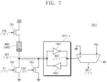
- FIG. 7 is a circuit diagram illustrating example configurations of a dendritic gate of FIG. 4 .
- the gate controlling circuit 1500 may output the signal STB having a logical value of “0”, the signal ST having a logical value of “1”, and the signal EXE having a logical value of “0” in response to the signal CS.
- the transistor TR 1 may be turned on in response to the signal STB having a logical value of “0”.
- a current may flow from the supply terminal of the operation voltage VDD to the memristor component MRD through the transistor TR 1 .
- the current flowing through the transistor TR 1 may flow to the node ND 1 through the memristor component MRD.
- the transistor TR 2 may be turned on in response to the signal ST having a logical value of “1”.
- a current may flow from the node ND 1 to the ground terminal through the transistor TR 2 .
- the transistor TR 3 may be turned off in response to the signal EXE having a logical value of “0”.
- the current flowing through the transistor TR 1 may be blocked by the memristor component MRD programmed to the HRS. As a current continuously flows from the node ND 1 to the ground terminal through the transistor TR 2 , a level of a voltage of the node ND 1 may decrease. Accordingly, the voltage of the node ND 1 may have a low level corresponding to the logical value of “0”.
- the inverter INV 1 may invert a logical value of “0” corresponding to a voltage formed at the node ND 1 .
- a logical value of “1” may be stored on the node ND 2 by the inverters INV 1 and INV 2 .
- the multiplexer MX may output the signal SEL 1 having a logical value of the signal PS 1 .
- the multiplexer MX may output the signal SEL 1 having a logical value of “1” in response to a pulse included in the signal PS 1 .
- Memory cells of the column corresponding to the dendritic gate 1611 may be activated for the re-training in response to the signal SEL 1 having the logical value of “1”, which will be described with reference to FIG. 12 .
- FIG. 8 is a circuit diagram illustrating example configurations of a dendritic gate of FIG. 4 .
- the gate controlling circuit 1500 may output the signal STB having a logical value of “0”, the signal ST having a logical value of “1”, and the signal EXE having a logical value of “0” in response to the signal CS.
- the transistor TR 1 may be turned on in response to the signal STB having a logical value of “0”.
- a current may flow from the supply terminal of the operation voltage VDD to the memristor component MRD through the transistor TR 1 .
- the current flowing through the transistor TR 1 may flow to the node ND 1 through the memristor component MRD programmed to the LRS.
- the transistor TR 2 may be turned on in response to the signal ST having a logical value of “1”.
- a current may flow from the node ND 1 to the ground terminal through the transistor TR 2 .
- the transistor TR 3 may be turned off in response to the signal EXE having a logical value of “0”.
- a level of a voltage formed at the node ND 1 may increase by the current flowing through the transistor TR 1 and the memristor component MRD programmed to the LRS. Accordingly, the voltage of the node ND 1 may have a high level corresponding to a logical value of “1”.
- the inverter INV 1 may invert a logical value of “1” corresponding to the voltage formed at the node ND 1 .
- a logical value of “0” may be stored on the node ND 2 by the inverters INV 1 and INV 2 .
- the multiplexer MX may output the signal SEL 1 having a logical value corresponding to the ground voltage.
- the multiplexer MX may output the signal SEL 1 having a logical value of “0”.
- Memory cells of the column corresponding to the dendritic gate 1611 may be deactivated in response to the signal SEL 1 having a logical value of “0”, which will be described with reference to FIG. 12 .
- FIG. 9 is a circuit diagram illustrating example operations of a dendritic gate of FIG. 4 .
- the processor 10 may output the signal CS such that the pre-training is performed on all the memory cells of the memristor array circuit 1200 .
- the processor 10 may output the signal CS such that all the memory cells are activated to provide information corresponding to input data to the user (i.e., to perform an inference operation).
- the gate controlling circuit 1500 may output the signal STB having a logical value of “1”, the signal ST having a logical value of “0”, and the signal EXE having a logical value of “1” in response to the signal CS.
- the transistor TR 1 may be turned off in response to the signal STB having a logical value of “1”.
- the transistor TR 2 may be turned off in response to the signal ST having a logical value of “0”.
- the transistor TR 3 may be turned on in response to the signal EXE having a logical value of “1”. A current may flow from the node ND 1 to the ground terminal through the transistor TR 3 . As a current flows from the node ND 1 to the ground terminal through the transistor TR 3 , a level of a voltage of the node ND 1 may decrease. Accordingly, the voltage of the node ND 1 may have a low level corresponding to a logical value of “0” regardless of the operations of the transistors TR 1 and TR 2 .
- the inverter INV 1 may invert a logical value of “0” corresponding to a voltage formed at the node ND 1 .
- a logical value of “1” may be stored on the node ND 2 by the inverters INV 1 and INV 2 .
- the multiplexer MX may output the signal SEL 1 having a logical value of the signal PS 1 .
- the multiplexer MX may output the signal SEL 1 having a logical value of “1” in response to a pulse included in the signal PS 1 .
- FIG. 10 is a circuit diagram illustrating an example configuration of a memristor array circuit of FIG. 1 .
- the memristor array circuit 1200 may include a memory cell array including “m” rows (“m” being a natural number) and “2n” columns.
- the memristor array circuit 1200 may include columns COL 11 and COL 12 to COLn 1 and COLn 2 .
- Each of the columns COL 11 and COL 12 to COLn 1 and COLn 2 may include “m” memory cells.
- Each of the memory cells may include a memristor component and a transistor.
- memory cells may include memristor components MR 1 and MR 2 , respectively.
- the signal SEL received from the gate circuit 1600 may include the signals SEL 1 to SELn respectively corresponding to the “2n” columns.
- the signals SEL 1 to SELn may be respectively received by the “2n” columns.
- Each of the signals SEL 1 to SELn may be received by two columns.
- the signal SEL 1 may be received by the columns COL 11 and COL 12
- the signal SELn may be received by the columns COLn 1 and COLn 2 . Because the signals SEL 1 to SELn are sequentially output from the gate circuit 1600 , the signals SEL 1 to SELn may be sequentially received.
- the voltage VIN received from the input circuit 1100 may include voltages VIN 1 to VINm respectively corresponding to the “m” rows. The voltages VIN 1 to VINm may be respectively received by the “m” rows.
- Gate terminals of the transistors may be connected with lines of the signal SEL received from the gate circuit 1600 .
- the gate terminals of the transistors included in the columns COL 11 and COL 12 may be connected with a line of the signal SEL 1
- the gate terminals of the transistors included in the columns COLn 1 and COLn 2 may be connected with a line of the signal SELn.
- Each of the memristor components may be connected between a line of the voltage VIN and the transistor.
- the memristor components may be connected between the corresponding transistors and lines of the voltages VIN 1 to VINm.
- the voltage VOUT of FIG. 1 may include voltages VOUT 11 and VOUT 12 to VOUTn 1 and VOUTn 2 of FIG. 10 .
- the voltage VOUT 11 may correspond to a sum of currents flowing through the memristor resistors and the transistors included in the column COL 11 .
- currents the levels of which are determined by levels of the voltages VIN 1 to VINm and resistance values of memristor resistors, may flow through transistors.
- the voltage VOUT 11 may be output from the column COL 11 by the currents flowing through the transistors.
- FIG. 11 is a circuit diagram illustrating example operations of a memristor array circuit of FIG. 10 .
- the pre-training may be performed on the memristor array circuit 1200 .
- the signals SEL 1 to SELn having a logical value of “1” may be received by the columns COL 11 and COL 12 to COLn 1 and COLn 2 for the pre-training. All the transistors included in the columns COL 11 and COL 12 to COLn 1 and COLn 2 may be turned on in response to the signals SEL 1 to SELn having a logical value of “1”.
- the memory cells of the columns COL 11 and COL 12 to COLn 1 and COLn 2 may be sequentially activated.
- the transistors included in the columns COL 11 and COL 12 to COLn 1 and COLn 2 may be sequentially turned on in the unit of column.
- the transistors of the columns COL 11 and COL 12 may be turned on in response to the signal SEL 1 received during a first time period.
- the transistors of the columns COLn 1 and COLn 2 may be turned on in response to the signal SELn.
- currents may flow through memristor components having particular resistance values from the lines of the voltages VIN 1 to VINm.
- Levels of the currents may correspond to the levels of the voltages VIN 1 to VINm, respectively.
- Resistance values of the memristor components may be changed by the currents flowing through the memristor components. Accordingly, the memristor components may have resistance values corresponding to the levels of the voltages VIN 1 to VINm.
- the memristor components may store input data as resistance values thereof. That is, the resistance values of the memristor components may be changed based on the input data.
- the levels of the voltages VIN 1 to VINm may indicate the input data for the pre-training.
- the input data may be associated with weights of the memristor components.
- the memristor array circuit 1200 may store weights for the pre-training.
- the memristor component MR 1 may have a relatively great resistance value by the voltage VIN 1 . That is, the memristor component MR 1 may be programmed to the HRS.
- the memristor component MR 2 may have any resistance value smaller than the resistance value corresponding to the HRS, by the voltage VIN 2 . That is, the memristor component MR 2 may be programmed to a state between the HRS and the LRS.
- a level of the voltage VOUT 11 may correspond to a sum of levels of currents flowing through memristor resistors of the column COL 11 .
- the levels of the currents flowing through the memristor resistors may correspond to resistance values of the memristor resistors, respectively. Because the memristor resistors store weights programmed by the voltages VIN 1 to VINm, the voltage VOUT 11 may have a level according to weights stored by the memristor resistors.
- the voltage VOUT 11 may indicate output data that are generated depending on the weights stored at the column COL 11 .
- columns of the memristor array circuit 1200 may output voltages VOUT 11 and VOUT 12 to VOUTn 1 and VOUTn 2 indicating pieces of output data generated depending on programmed weights.
- the voltages VOUT 11 and VOUT 12 to VOUTn 1 and VOUTn 2 may be sequentially output.
- the voltages VOUT 11 and VOUT 12 may be output during a first time period, and the voltages VOUTn 1 and VOUTn 2 during a second time period after the first time period.
- the processor 10 may obtain defect information from result data generated by the calculating circuit 1300 based on the voltages VOUT 11 and VOUT 12 to VOUTn 1 and VOUTn 2 .
- FIG. 12 is a circuit diagram illustrating example operations of a memristor array circuit of FIG. 10 .
- the re-training may be performed on the memristor array circuit 1200 .
- the columns COL 11 and COL 12 may be selected as target columns by the processor 10
- the columns COLn 1 and COLn 2 may not be selected as target columns by the processor 10 .
- the signal SEL 1 having a logical value of “1” may be received by the columns COL 11 and COL 12
- the signal SELn having a logical value of “0” may be received by the columns COLn 1 and COLn 2 .
- Transistors included in the columns COL 11 and COL 12 may be turned on in response to the signal SEL 1 having a logical value of “1”.
- Transistors included in the columns COLn 1 and COLn 2 may be turned off in response to the signal SEL 1 having a logical value of “0”.
- currents may flow through memristor components of the columns COL 11 and COL 12 from lines of the voltages VIN 1 to VINm.
- Levels of the currents flowing through the memristor components may correspond to the levels of the voltages VIN 1 to VINm, respectively.
- Resistance values of the memristor components may be changed by the currents flowing through the memristor components. For example, a resistance value of the memristor component MR 1 may decrease, and a resistance value of the memristor component MR 2 may increase.
- the memristor components of the columns COL 11 and COL 12 may store input data for the re-training as resistance values thereof. However, because currents are blocked by the transistors of the columns COLn 1 and COLn 2 , the re-training for the memristor components of the columns COLn 1 and COLn 2 may be omitted. That is, the voltages VOUTn 1 and VOUTn 2 may not be output from the columns COLn 1 and COLn 2 .
- the levels of the voltages VIN 1 to VINm may indicate the input data for the re-training. For example, the levels of the voltages VIN 1 to VINm may be associated with weights of the memristor components.
- the memristor array circuit 1200 may store weights through the re-training.
- the memristor component MR 1 may have a relatively great weight (or a relatively great resistance value) by the voltage VIN 1 . That is, the memristor component MR 1 may be programmed to the HRS.
- the memristor component MR 2 may have a relatively small weight (or any resistance value smaller than a resistance value corresponding to the HRS) by the voltage VIN 2 . That is, the memristor component MR 2 may be programmed to a state between the HRS and the LRS.
- the re-training is performed depending on whether a memory cell includes a defect, costs (e.g., a time or energy) necessary for the re-training may increase.
- costs e.g., a time or energy
- the re-training is performed only on target columns (e.g., the columns COL 11 and COL 12 ) selected by the processor 10 and the re-training is not performed on columns not being the target columns, a time taken to perform the re-training may decrease.
- energy e.g., a power
- FIG. 13 is a circuit diagram illustrating an example configuration of a calculating circuit of FIG. 1 .
- the calculating circuit 1300 may include adders 1311 to 1321 and function circuits 1312 to 1322 .
- the number of the adders 1311 to 1321 and the number of the function circuits 1312 to 1322 may correspond to the number of columns included in the memristor array circuit 1200 .
- the calculating circuit 1300 may include “n” adders 1311 to 1321 and “n” function circuits 1312 to 1322 .
- the adders 1311 to 1321 may receive the voltages VOUT 11 and VOUT 12 to VOUTn 1 to VOUTn 2 from the memristor array circuit 1200 .
- the adder 1311 may receive the voltages VOUT 11 and VOUT 12
- the adder 1321 may receive the voltages VOUTn 1 and VOUTn 2 .
- the adders 1311 to 1321 may respectively output the voltages VOUT 1 to VOUTn based on the voltages VOUT 11 and VOUT 12 to VOUTn 1 to VOUTn 2 .
- the adder 1311 may output a voltage VOUT 1 based on the voltages VOUT 11 and VOUT 12
- the adder 1321 may output a voltage VOUTn based on the voltages VOUTn 1 and VOUTn 2 .
- the voltages VOUT 11 and VOUT 12 to VOUTn 1 to VOUTn 2 indicate pieces of output data generated by the columns COL 11 and COL 12 to COLn 1 and COLn 2 , respectively, the voltages VOUT 1 to VOUTn may indicate the pieces of output data generated by the columns COL 11 and COL 12 to COLn 1 and COLn 2 , respectively.
- the adders 1311 to 1321 may calculate differences between levels of received voltages.
- a level of the voltage VOUT 1 output from the adder 1311 may correspond to a difference between a level of the voltage VOUT 11 and a level of the voltage VOUT 12 .
- a level of the voltage VOUTn output from the adder 1321 may correspond to a difference between a level of the voltage VOUTn 1 and a level of the voltage VOUTn 2 .
- the function circuits 1312 to 1322 may include electronic circuits for implementing an activation function according to various algorithms.
- the function circuits 1312 to 1322 may perform a calculation according to an activation function based on output data of the voltages VOUT 1 to VOUTn. Accordingly, a signal ODAT 1 may indicate result data calculated from output data of the voltage VOUT 1 (i.e., output data generated by the columns COL 11 and COL 12 ).
- a signal ODATn may indicate result data calculated from output data of the voltage VOUTn (i.e., output data generated by the columns COLn 1 and COLn 2 ).
- the “n” signals ODAT 1 to ODATn may be output to the processor 10 as the signal ODAT of FIG. 1 .
- the processor 10 may perform various operations based on result data indicated by the signals ODAT 1 to ODATn. For example, the processor 10 may obtain defect information based on the result data.
- FIG. 14 is a block diagram illustrating an example electronic device including a neural network system according to an embodiment of the inventive concept.
- an electronic device 2000 may be one of a personal computer, a workstation, a notebook computer, a mobile device, etc.
- the electronic device 2000 may include a processor 2100 , a memory 2200 , storage 2300 , a communication device 2400 , a user interface 2500 , a neural network system 2600 , and a bus 2700 .
- the electronic device 2000 may further include other components (e.g., various sensors and a power supply) that are not illustrated in FIG. 14 .
- the electronic device 2000 may not include one or more of the components illustrated in FIG. 14 .
- the processor 2100 may control overall operations of the electronic device 2000 .
- the processor 2100 that is a central control device may process operations necessary for an operation of the electronic device 2000 .
- the processor 2100 may process data for controlling operations of the electronic device 2000 .
- the processor 2100 may be one of a general-purpose processor, a workstation processor, an application processor, etc.
- the processor 2100 may include one processor core (i.e., a single core) or may include a plurality of processor cores (i.e., a multi-core).
- the processor 2100 may include a multi-core such as a dual-core, a quad-core, a hexa-core, or the like.
- the processor 2100 may include the processor 10 of FIG. 1 .
- the processor 10 may generate input data for the pre-training and the re-training of the neural network system 2600 .
- the processor 2100 may generate input data corresponding to a question input by the user.
- the processor 2100 may obtain defect information based on result data provided from the neural network system 2600 .
- the memory 2200 may store data processed or to be processed by the processor 2100 .
- the memory 2200 may include a volatile memory such as a static random access memory (SRAM), a dynamic RAM (DRAM), a synchronous DRAM (SDRAM), etc. or a nonvolatile memory such as a flash memory, a phase-change RAM (PRAM), a magneto-resistive RAM (MRAM), a resistive RAM (ReRAM), a ferroelectric RAM (FRAM), etc.
- the memory 2200 may include heterogeneous memories.
- the storage 2300 may store data regardless of whether a power is supplied.
- the storage 2300 may be a storage medium, which includes a nonvolatile memory, such as a hard disk drive (HDD), a solid state drive (SSD), a secure digital (SD) card, a universal serial bus (USB) memory device, or the like.
- a nonvolatile memory such as a hard disk drive (HDD), a solid state drive (SSD), a secure digital (SD) card, a universal serial bus (USB) memory device, or the like.
- the communication device 2400 may include a transmission unit and a reception unit.
- the electronic device 2000 may communicate with another electronic device through the communication device 2400 to transmit and/or receive data.
- the user interface 2500 may provide an input/output of an instruction or data between the user and the electronic device 2000 .
- the user interface 2500 may include a physical device such as an input device and/or an output device.
- the input device may include a keyboard, a mouse, a touchscreen, a scanner, a joystick, a voice recognition device, a motion recognition device, or an eyeball recognition device
- the output device may include a monitor, a display device, a projector, a speaker, or a plotter.
- the user may input an instruction through the user interface 2500 for the purpose of obtaining an answer to a question.
- the user interface 2500 may provide the user with information about the answer corresponding to the question.
- the neural network system 2600 may include the neural network system 1000 of FIG. 1 . As described with reference to FIGS. 1 to 13 , the neural network system 2600 may operate the signals CS and IDAT received from the processor 2100 . For example, the neural network system 2600 may be pre-trained and re-trained based on the signals CS and IDAT, and result data that indicate the answer to the question input by the user may be output by the trained neural network system 2600 .
- the bus 2700 may provide a communication path between the components of the electronic device 2000 .
- the processor 2100 , the memory 2200 , the storage 2300 , the communication device 2400 , the user interface 2500 , and the neural network system 2600 may exchange data with each other through the bus 2700 .
- the bus 2700 may be configured to support various communication formats used in the electronic device 2000 .
- a time and a power necessary to train a neural network may decrease.
Abstract
Description
Claims (20)
Applications Claiming Priority (2)
| Application Number | Priority Date | Filing Date | Title |
|---|---|---|---|
| KR1020190032866A KR102368962B1 (en) | 2019-03-22 | 2019-03-22 | Neural network system including gate circuit for controlling memristor array circuit |
| KR10-2019-0032866 | 2019-03-22 |
Publications (2)
| Publication Number | Publication Date |
|---|---|
| US20200302277A1 US20200302277A1 (en) | 2020-09-24 |
| US11727253B2 true US11727253B2 (en) | 2023-08-15 |
Family
ID=72514576
Family Applications (1)
| Application Number | Title | Priority Date | Filing Date |
|---|---|---|---|
| US16/682,420 Active 2041-10-01 US11727253B2 (en) | 2019-03-22 | 2019-11-13 | Neural network system including gate circuit for controlling memristor array circuit |
Country Status (2)
| Country | Link |
|---|---|
| US (1) | US11727253B2 (en) |
| KR (1) | KR102368962B1 (en) |
Families Citing this family (3)
| Publication number | Priority date | Publication date | Assignee | Title |
|---|---|---|---|---|
| CN112734022B (en) * | 2021-02-02 | 2023-12-19 | 郑州轻工业大学 | Four-character memristor neural network circuit with recognition and sequencing functions |
| KR102514652B1 (en) * | 2021-11-19 | 2023-03-29 | 서울대학교산학협력단 | Weight transfer apparatus for neuromorphic devices and weight transfer method using the same |
| CN116523011B (en) * | 2023-07-03 | 2023-09-15 | 中国人民解放军国防科技大学 | Memristor-based binary neural network layer circuit and binary neural network training method |
Citations (10)
| Publication number | Priority date | Publication date | Assignee | Title |
|---|---|---|---|---|
| US20140122402A1 (en) * | 2011-06-30 | 2014-05-01 | Commissariat A L'energie Atomique Et Aux Energies Alternatives | Network of artificial neurons based on complementary memristive devices |
| US20170011290A1 (en) * | 2015-07-06 | 2017-01-12 | University Of Dayton | On-chip training of memristor crossbar neuromorphic processing systems |
| KR20170024605A (en) | 2014-06-05 | 2017-03-07 | 마이크론 테크놀로지, 인크 | Apparatuses and methods for parity determination using sensing circuitry |
| KR20180009315A (en) | 2016-07-18 | 2018-01-26 | 아이엠이씨 브이제트더블유 | Hardware implementation of a temporal memory system |
| JP6293963B1 (en) | 2017-08-31 | 2018-03-14 | Tdk株式会社 | Array control device including neuromorphic element, discretization step size calculation method and program |
| US20180181867A1 (en) | 2016-12-21 | 2018-06-28 | Axis Ab | Artificial neural network class-based pruning |
| US20180276539A1 (en) | 2017-03-22 | 2018-09-27 | Micron Technology, Inc. | Apparatuses and methods for operating neural networks |
| US20180300619A1 (en) | 2017-04-17 | 2018-10-18 | SK Hynix Inc. | Synapse and a synapse array |
| US10115894B2 (en) | 2016-06-20 | 2018-10-30 | Massachusetts Institute Of Technology | Apparatus and methods for electrical switching |
| US20190228287A1 (en) * | 2018-01-19 | 2019-07-25 | International Business Machines Corporation | Neuromorphic chip for updating precise synaptic weight values |
-
2019
- 2019-03-22 KR KR1020190032866A patent/KR102368962B1/en active IP Right Grant
- 2019-11-13 US US16/682,420 patent/US11727253B2/en active Active
Patent Citations (17)
| Publication number | Priority date | Publication date | Assignee | Title |
|---|---|---|---|---|
| US20140122402A1 (en) * | 2011-06-30 | 2014-05-01 | Commissariat A L'energie Atomique Et Aux Energies Alternatives | Network of artificial neurons based on complementary memristive devices |
| US10249350B2 (en) | 2014-06-05 | 2019-04-02 | Micron Technology, Inc. | Apparatuses and methods for parity determination using sensing circuitry |
| KR20170024605A (en) | 2014-06-05 | 2017-03-07 | 마이크론 테크놀로지, 인크 | Apparatuses and methods for parity determination using sensing circuitry |
| US20170011290A1 (en) * | 2015-07-06 | 2017-01-12 | University Of Dayton | On-chip training of memristor crossbar neuromorphic processing systems |
| US10115894B2 (en) | 2016-06-20 | 2018-10-30 | Massachusetts Institute Of Technology | Apparatus and methods for electrical switching |
| KR20190020056A (en) | 2016-06-20 | 2019-02-27 | 메사추세츠 인스티튜트 오브 테크놀로지 | Apparatus and methods for electrical switching |
| KR20180009315A (en) | 2016-07-18 | 2018-01-26 | 아이엠이씨 브이제트더블유 | Hardware implementation of a temporal memory system |
| US10452972B2 (en) | 2016-07-18 | 2019-10-22 | Imec Vzw | Hardware implementation of a temporal memory system |
| US20180181867A1 (en) | 2016-12-21 | 2018-06-28 | Axis Ab | Artificial neural network class-based pruning |
| KR20180072562A (en) | 2016-12-21 | 2018-06-29 | 엑시스 에이비 | Artificial neural network class-based pruning |
| KR20190121859A (en) | 2017-03-22 | 2019-10-28 | 마이크론 테크놀로지, 인크 | Apparatus and method for operating neural network |
| US20180276539A1 (en) | 2017-03-22 | 2018-09-27 | Micron Technology, Inc. | Apparatuses and methods for operating neural networks |
| US20180300619A1 (en) | 2017-04-17 | 2018-10-18 | SK Hynix Inc. | Synapse and a synapse array |
| KR20180116637A (en) | 2017-04-17 | 2018-10-25 | 에스케이하이닉스 주식회사 | A Synapse Having Dual Memristors and a Synapse Array of a Neuromorphic Device Including the Synapse |
| JP6293963B1 (en) | 2017-08-31 | 2018-03-14 | Tdk株式会社 | Array control device including neuromorphic element, discretization step size calculation method and program |
| US20200272891A1 (en) | 2017-08-31 | 2020-08-27 | Tdk Corporation | Controller of array including neuromorphic element, method of arithmetically operating discretization step size, and program |
| US20190228287A1 (en) * | 2018-01-19 | 2019-07-25 | International Business Machines Corporation | Neuromorphic chip for updating precise synaptic weight values |
Also Published As
| Publication number | Publication date |
|---|---|
| KR20200113106A (en) | 2020-10-06 |
| KR102368962B1 (en) | 2022-03-03 |
| US20200302277A1 (en) | 2020-09-24 |
Similar Documents
| Publication | Publication Date | Title |
|---|---|---|
| JP6477924B2 (en) | Memristor neuromorphological circuit and method for training memristor neuromorphological circuit | |
| US11727253B2 (en) | Neural network system including gate circuit for controlling memristor array circuit | |
| US9715655B2 (en) | Method and apparatus for performing close-loop programming of resistive memory devices in crossbar array based hardware circuits and systems | |
| JPWO2019049741A1 (en) | Neural network arithmetic circuit using non-volatile semiconductor memory device | |
| CN110674933A (en) | Pipeline technique for improving neural network inference accuracy | |
| JP6956191B2 (en) | Neural network arithmetic circuit using non-volatile semiconductor memory element | |
| US11157803B2 (en) | Neuromorphic device including a synapse having a variable resistor and a transistor connected in parallel with each other | |
| US11620505B2 (en) | Neuromorphic package devices and neuromorphic computing systems | |
| US11087204B2 (en) | Resistive processing unit with multiple weight readers | |
| US11119674B2 (en) | Memory devices and methods for operating the same | |
| US11354569B2 (en) | Neural network computation circuit including semiconductor storage elements | |
| US11790985B2 (en) | Electronic device for configuring neural network | |
| US20180349761A1 (en) | Synapse array of neuromorphic device including synapses having ferro-electric field effect transistors and operation method of the same | |
| US11227211B2 (en) | Neuromorphic device including a synapse having a plurality of synapse cells | |
| TWI699711B (en) | Memory devices and manufacturing method thereof | |
| US11321608B2 (en) | Synapse memory cell driver | |
| US11210581B2 (en) | Synapse and a synapse array | |
| KR102409859B1 (en) | Memory cells configured to generate weighted inputs for neural networks | |
| US10002658B1 (en) | Dynamic random-access memory with embedded artificial neural network functionality | |
| CN115796252A (en) | Weight writing method and device, electronic equipment and storage medium | |
| Lu et al. | NVMLearn: a simulation platform for non-volatile-memory-based deep learning hardware | |
| Yan et al. | Neuromorphic Computing Systems with Emerging Nonvolatile Memories: A Circuits and Systems Perspective | |
| KR102511526B1 (en) | Hardware-based artificial neural network device | |
| Singh et al. | Finite State Automata Design using 1T1R ReRAM Crossbar | |
| CN115796250A (en) | Weight deployment method and device, electronic equipment and storage medium |
Legal Events
| Date | Code | Title | Description |
|---|---|---|---|
| FEPP | Fee payment procedure |
Free format text: ENTITY STATUS SET TO UNDISCOUNTED (ORIGINAL EVENT CODE: BIG.); ENTITY STATUS OF PATENT OWNER: SMALL ENTITY |
|
| AS | Assignment |
Owner name: KOOKMIN UNIVERSITY INDUSTRY ACADEMY COOPERATION FOUNDATION, KOREA, REPUBLIC OF Free format text: ASSIGNMENT OF ASSIGNORS INTEREST;ASSIGNOR:MIN, KYEONG SIK;REEL/FRAME:051022/0567 Effective date: 20191104 |
|
| FEPP | Fee payment procedure |
Free format text: ENTITY STATUS SET TO SMALL (ORIGINAL EVENT CODE: SMAL); ENTITY STATUS OF PATENT OWNER: SMALL ENTITY |
|
| STPP | Information on status: patent application and granting procedure in general |
Free format text: DOCKETED NEW CASE - READY FOR EXAMINATION |
|
| STPP | Information on status: patent application and granting procedure in general |
Free format text: NON FINAL ACTION MAILED |
|
| STPP | Information on status: patent application and granting procedure in general |
Free format text: RESPONSE TO NON-FINAL OFFICE ACTION ENTERED AND FORWARDED TO EXAMINER |
|
| STPP | Information on status: patent application and granting procedure in general |
Free format text: FINAL REJECTION MAILED |
|
| STPP | Information on status: patent application and granting procedure in general |
Free format text: PUBLICATIONS -- ISSUE FEE PAYMENT VERIFIED |
|
| STCF | Information on status: patent grant |
Free format text: PATENTED CASE |